EP0632426B1 - Liquid crystal display device and method for driving the same - Google Patents
Liquid crystal display device and method for driving the same Download PDFInfo
- Publication number
- EP0632426B1 EP0632426B1 EP94304813A EP94304813A EP0632426B1 EP 0632426 B1 EP0632426 B1 EP 0632426B1 EP 94304813 A EP94304813 A EP 94304813A EP 94304813 A EP94304813 A EP 94304813A EP 0632426 B1 EP0632426 B1 EP 0632426B1
- Authority
- EP
- European Patent Office
- Prior art keywords
- voltage
- liquid crystal
- ferroelectric liquid
- switching device
- pixel
- Prior art date
- Legal status (The legal status is an assumption and is not a legal conclusion. Google has not performed a legal analysis and makes no representation as to the accuracy of the status listed.)
- Expired - Lifetime
Links
Images


Classifications
-
- G—PHYSICS
- G09—EDUCATION; CRYPTOGRAPHY; DISPLAY; ADVERTISING; SEALS
- G09G—ARRANGEMENTS OR CIRCUITS FOR CONTROL OF INDICATING DEVICES USING STATIC MEANS TO PRESENT VARIABLE INFORMATION
- G09G3/00—Control arrangements or circuits, of interest only in connection with visual indicators other than cathode-ray tubes
- G09G3/20—Control arrangements or circuits, of interest only in connection with visual indicators other than cathode-ray tubes for presentation of an assembly of a number of characters, e.g. a page, by composing the assembly by combination of individual elements arranged in a matrix no fixed position being assigned to or needed to be assigned to the individual characters or partial characters
- G09G3/34—Control arrangements or circuits, of interest only in connection with visual indicators other than cathode-ray tubes for presentation of an assembly of a number of characters, e.g. a page, by composing the assembly by combination of individual elements arranged in a matrix no fixed position being assigned to or needed to be assigned to the individual characters or partial characters by control of light from an independent source
- G09G3/36—Control arrangements or circuits, of interest only in connection with visual indicators other than cathode-ray tubes for presentation of an assembly of a number of characters, e.g. a page, by composing the assembly by combination of individual elements arranged in a matrix no fixed position being assigned to or needed to be assigned to the individual characters or partial characters by control of light from an independent source using liquid crystals
- G09G3/3611—Control of matrices with row and column drivers
- G09G3/3648—Control of matrices with row and column drivers using an active matrix
- G09G3/3655—Details of drivers for counter electrodes, e.g. common electrodes for pixel capacitors or supplementary storage capacitors
-
- G—PHYSICS
- G09—EDUCATION; CRYPTOGRAPHY; DISPLAY; ADVERTISING; SEALS
- G09G—ARRANGEMENTS OR CIRCUITS FOR CONTROL OF INDICATING DEVICES USING STATIC MEANS TO PRESENT VARIABLE INFORMATION
- G09G3/00—Control arrangements or circuits, of interest only in connection with visual indicators other than cathode-ray tubes
- G09G3/20—Control arrangements or circuits, of interest only in connection with visual indicators other than cathode-ray tubes for presentation of an assembly of a number of characters, e.g. a page, by composing the assembly by combination of individual elements arranged in a matrix no fixed position being assigned to or needed to be assigned to the individual characters or partial characters
- G09G3/34—Control arrangements or circuits, of interest only in connection with visual indicators other than cathode-ray tubes for presentation of an assembly of a number of characters, e.g. a page, by composing the assembly by combination of individual elements arranged in a matrix no fixed position being assigned to or needed to be assigned to the individual characters or partial characters by control of light from an independent source
- G09G3/36—Control arrangements or circuits, of interest only in connection with visual indicators other than cathode-ray tubes for presentation of an assembly of a number of characters, e.g. a page, by composing the assembly by combination of individual elements arranged in a matrix no fixed position being assigned to or needed to be assigned to the individual characters or partial characters by control of light from an independent source using liquid crystals
- G09G3/3611—Control of matrices with row and column drivers
- G09G3/3648—Control of matrices with row and column drivers using an active matrix
- G09G3/3651—Control of matrices with row and column drivers using an active matrix using multistable liquid crystals, e.g. ferroelectric liquid crystals
-
- G—PHYSICS
- G09—EDUCATION; CRYPTOGRAPHY; DISPLAY; ADVERTISING; SEALS
- G09G—ARRANGEMENTS OR CIRCUITS FOR CONTROL OF INDICATING DEVICES USING STATIC MEANS TO PRESENT VARIABLE INFORMATION
- G09G3/00—Control arrangements or circuits, of interest only in connection with visual indicators other than cathode-ray tubes
- G09G3/20—Control arrangements or circuits, of interest only in connection with visual indicators other than cathode-ray tubes for presentation of an assembly of a number of characters, e.g. a page, by composing the assembly by combination of individual elements arranged in a matrix no fixed position being assigned to or needed to be assigned to the individual characters or partial characters
- G09G3/34—Control arrangements or circuits, of interest only in connection with visual indicators other than cathode-ray tubes for presentation of an assembly of a number of characters, e.g. a page, by composing the assembly by combination of individual elements arranged in a matrix no fixed position being assigned to or needed to be assigned to the individual characters or partial characters by control of light from an independent source
- G09G3/36—Control arrangements or circuits, of interest only in connection with visual indicators other than cathode-ray tubes for presentation of an assembly of a number of characters, e.g. a page, by composing the assembly by combination of individual elements arranged in a matrix no fixed position being assigned to or needed to be assigned to the individual characters or partial characters by control of light from an independent source using liquid crystals
- G09G3/3611—Control of matrices with row and column drivers
- G09G3/3648—Control of matrices with row and column drivers using an active matrix
- G09G3/3659—Control of matrices with row and column drivers using an active matrix the addressing of the pixel involving the control of two or more scan electrodes or two or more data electrodes, e.g. pixel voltage dependant on signal of two data electrodes
-
- G—PHYSICS
- G09—EDUCATION; CRYPTOGRAPHY; DISPLAY; ADVERTISING; SEALS
- G09G—ARRANGEMENTS OR CIRCUITS FOR CONTROL OF INDICATING DEVICES USING STATIC MEANS TO PRESENT VARIABLE INFORMATION
- G09G2300/00—Aspects of the constitution of display devices
- G09G2300/08—Active matrix structure, i.e. with use of active elements, inclusive of non-linear two terminal elements, in the pixels together with light emitting or modulating elements
- G09G2300/0809—Several active elements per pixel in active matrix panels
- G09G2300/0814—Several active elements per pixel in active matrix panels used for selection purposes, e.g. logical AND for partial update
-
- G—PHYSICS
- G09—EDUCATION; CRYPTOGRAPHY; DISPLAY; ADVERTISING; SEALS
- G09G—ARRANGEMENTS OR CIRCUITS FOR CONTROL OF INDICATING DEVICES USING STATIC MEANS TO PRESENT VARIABLE INFORMATION
- G09G2300/00—Aspects of the constitution of display devices
- G09G2300/08—Active matrix structure, i.e. with use of active elements, inclusive of non-linear two terminal elements, in the pixels together with light emitting or modulating elements
- G09G2300/0809—Several active elements per pixel in active matrix panels
- G09G2300/0842—Several active elements per pixel in active matrix panels forming a memory circuit, e.g. a dynamic memory with one capacitor
- G09G2300/0852—Several active elements per pixel in active matrix panels forming a memory circuit, e.g. a dynamic memory with one capacitor being a dynamic memory with more than one capacitor
-
- G—PHYSICS
- G09—EDUCATION; CRYPTOGRAPHY; DISPLAY; ADVERTISING; SEALS
- G09G—ARRANGEMENTS OR CIRCUITS FOR CONTROL OF INDICATING DEVICES USING STATIC MEANS TO PRESENT VARIABLE INFORMATION
- G09G2310/00—Command of the display device
- G09G2310/02—Addressing, scanning or driving the display screen or processing steps related thereto
- G09G2310/0235—Field-sequential colour display
-
- G—PHYSICS
- G09—EDUCATION; CRYPTOGRAPHY; DISPLAY; ADVERTISING; SEALS
- G09G—ARRANGEMENTS OR CIRCUITS FOR CONTROL OF INDICATING DEVICES USING STATIC MEANS TO PRESENT VARIABLE INFORMATION
- G09G2310/00—Command of the display device
- G09G2310/02—Addressing, scanning or driving the display screen or processing steps related thereto
- G09G2310/0243—Details of the generation of driving signals
- G09G2310/0251—Precharge or discharge of pixel before applying new pixel voltage
-
- G—PHYSICS
- G09—EDUCATION; CRYPTOGRAPHY; DISPLAY; ADVERTISING; SEALS
- G09G—ARRANGEMENTS OR CIRCUITS FOR CONTROL OF INDICATING DEVICES USING STATIC MEANS TO PRESENT VARIABLE INFORMATION
- G09G2310/00—Command of the display device
- G09G2310/06—Details of flat display driving waveforms
-
- G—PHYSICS
- G09—EDUCATION; CRYPTOGRAPHY; DISPLAY; ADVERTISING; SEALS
- G09G—ARRANGEMENTS OR CIRCUITS FOR CONTROL OF INDICATING DEVICES USING STATIC MEANS TO PRESENT VARIABLE INFORMATION
- G09G3/00—Control arrangements or circuits, of interest only in connection with visual indicators other than cathode-ray tubes
- G09G3/20—Control arrangements or circuits, of interest only in connection with visual indicators other than cathode-ray tubes for presentation of an assembly of a number of characters, e.g. a page, by composing the assembly by combination of individual elements arranged in a matrix no fixed position being assigned to or needed to be assigned to the individual characters or partial characters
- G09G3/2007—Display of intermediate tones
- G09G3/2011—Display of intermediate tones by amplitude modulation
Definitions
- the present invention relates to a liquid crystal display device and a method for driving the same.
- LCD devices Liquid crystal display devices
- CRTs cathode ray tubes
- LCD devices using a nematic liquid crystal material are in wide use.
- Examples of LCD devices using a nematic liquid crystal material are twisted nematic (hereinafter, referred to as "TN”) LCD devices and supertwisted birefringence effect (hereinafter, referred to as "SBE”) LCD devices.
- TN twisted nematic
- SBE supertwisted birefringence effect
- the TN LCD devices As the number of the scanning lines is increased, the time period during which application of a voltage to each scanning line is permitted for putting the liquid crystal molecules into an "ON" state or an “OFF” state becomes shorter, resulting in an insufficient contrast. For this reason, the TN LCD devices are not suitable for large capacity display devices.
- SBE LCD devices or double layer SBE LCD devices have been developed. However, in such LCD devices, as the number of the scanning lines is increased, the contrast of displayed images and the response speed are still low. Currently, the maximum possible display capacity is approximately 800 x 1024 lines.
- display devices using a nematic liquid crystal material have a serious problem in that the viewing angle is narrow.
- the SBE LCD devices or the double layer SBE LCD devices satisfactory values have not been obtained with regard to the contrast of displayed images or the response speed.
- TFTs thin film transistors
- a large display capacity of, for example, 1000 x 1000 lines and a high contrast are obtained.
- the active matrix LCD devices generally use a TN liquid crystal material, the above-mentioned problems in the viewing angle and the response speed still remain.
- N. A. Clark and S. T. Lagerwall proposed an LCD device using a chiral smectic C liquid crystal material, namely, a ferroelectric liquid crystal material (hereinafter, referred to as the "FLC material") in order to solve these problems (see, e.g., Appl. Phys. Lett., 36, 899 (1980); the United States Patent No. 4,367,924; and Japanese Laid-Open Patent Publication No. 56-107216).
- FLC material ferroelectric liquid crystal material
- the LCD device proposed by Clark and Lagerwall uses a rotational force for aligning the orientation of the FLC molecules obtained by the spontaneous polarization thereof and the polarity of the electric field.
- FIGs 3A through 3E schematically illustrate the spontaneous polarization of the FLC molecules and the electrooptic effect.
- the FLC molecules initially have a helical structure.
- the helix is loosened as is shown Figure 3B .
- the FLC molecules show bistability; that is, the liquid crystal layer includes a stable area where the FLC molecules are stable while tilted by an angle of + ⁇ with respect to the normal line 900 relative to a surface of the liquid crystal layer and a stable area where the FLC molecules are stable while tilted by an angle of - ⁇ with respect to the normal line 900 .
- the orientations of the FLC molecules obtained by the spontaneous polarization thereof can be uniformly aligned as is shown in Figure 3C .
- the FLC molecules are aligned in the opposite direction as is shown Figure 3D .
- the alignment orientation of the FLC molecules obtained by the voltage application is maintained by the alignment restricting force of the interface between the liquid crystal layer and the substrate even after the voltage application is stopped.
- a memory function can be obtained. Since the spontaneous polarization and the electric field directly effect the driving of the FLC molecules, the time required for driving the FLC molecules in a switching manner is 1/1000 or shorter; that is, the response speed is quite high. Due to such a high response speed, high speed display is possible. However, there are still problems in that it is difficult to obtain a uniform alignment of the FLC molecules for realizing a high contrast and to display an image having various tones.
- FLC molecules have been considered to have only two stable alignment states. Recently, an intermediate state between these two states is considered obtainable by applying an electric field in a certain manner.
- This is disclosed in, for example, Japanese Laid-Open Patent Publication No. 3-242624; Japanese Laid-Open Patent Publication No. 3-243915; Mori et al., Preprints of the 16th Symposium on Liquid Crystal, Japan, 3K111 (1990); Toyota et al., Preprints of the 16th Symposium on Liquid Crystal, Japan, 3K112 (1990); Japanese Laid-Open Patent Publication No. 4-212126; Japanese Laid-Open Patent Publication No. 4-218023; Matsui et al., Preprints of the 17th Symposium on Liquid Crystal, Japan, 3F301 (1991); and K. Nito et al., Proc. IDRC, 179 (1991).
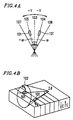
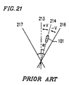
- the intermediate stable alignment state is obtained in the following manner.
- Clark-Lager-wall type FLC molecules 101 usually have two stable alignment states 104 and 105 .
- reference numeral 103 denotes a central line which bisects an angle defined by the principal axes of the FLC molecules 101 in the stable alignment states 104 and 105 .
- the designation ⁇ indicates an angle between the principal axis of the FLC molecule 101 in the stable alignment state 104 and the central line 103 .
- the designation - ⁇ indicates an angle between the principal axis of the FLC molecule 101 in the stable alignment state 105 and the central line 103 .
- Reference numerals 106 and 107 denote tilting axes, respectively.
- such FLC molecules 101 are aligned to have only one stable alignment state as is shown in Figure 21 .
- the stable alignment state is indicated by reference numeral 214 , and this state corresponds to one of either state 104 or 105 in Figure 4A .
- a central line 213 corresponds to the central line 103
- tilting axes 216 and 217 correspond to the tilting axes 106 and 107 in Figure 4A .
- the principal axis of the FLC molecule 101 is moved to be oriented in any direction between the tilting angles 216 and 217 . In this manner, an intermediate stable alignment state is realized.
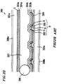
- an FLCD (ferroelectric liquid crystal display) device 200 including TFTs as is shown in Figure 20 is used.
- the FLCD device 200 includes two glass substrates 201a and 201b located opposite each other.
- a transparent counter electrode L formed of indium tin oxide (hereinafter, referred to as "ITO") is provided on a surface of the glass substrate 201a .
- the counter electrode L is coated with a transparent insulation layer 203a formed of Ta 2 O 5 or the like.
- active elements in this case TFTs B each including a gate electrode G , a source electrode S , a drain electrode D , a semiconductor layer 205 and an insulation layer 202 , are provided.
- the active elements are used as switching devices.
- transparent pixel electrodes 209 formed of ITO and each connected to a corresponding drain electrode D are provided on the insulation layer 202 .
- the TFTs B and the pixel electrodes 209 are covered with a transparent insulation layer 203b formed of Ta 2 O 5 .
- the insulation layers 203a and 203b are respectively covered with transparent alignment layers 204a and 204b which are formed of polyvinyl alcohol (hereinafter, referred to as "PVA") or the like.
- PVA polyvinyl alcohol
- the two glass substrates 201a and 201b having the above-mentioned laminate thereon are assembled together with spacers 206 (only one of which is shown in Figure 20 ) therebetween.
- spacers 206 only one of which is shown in Figure 20
- a space interposed between the alignment layers 204a and 204b is filled with an FLC layer 207 .
- the outer surface of the glass substrate 201a is covered with a polarizing plate 208a ; and the outer surface of the glass substrate 201b is covered with a polarizing plate 208b .
- the respective polarizing axes of the polarizing plates 208a and 208b are perpendicular to each other.
- Each pixel electrode 209 , an area of the FLC layer 207 in correspondence with the pixel electrode 209 , and an area of the counter electrode L in correspondence with the pixel electrode 209 form a pixel in the FLCD device 200 .
- Japanese Laid-Open Patent Publication Nos. 3-242624 and 3-243915 each disclose a sequential tone display method using the FLCD device 200 .
- the FLCD device 200 disclosed in these publications only one of the two alignment layers 204a and 204b is treated for alignment by, for example, rubbing.
- the FLC molecules 101 in the FLC layer 207 are stable in only one stable alignment state 214 .
- the FLC molecules 101 When a positive electric field is applied to the FLC molecules 101 having only one stable alignment state 214 , the FLC molecules 101 are subjected to a force directed toward the tilting axis 217 and also to a force directed back toward the stable alignment state 214 . As a result, the FLC molecules 101 stop at a position where the two oppositely directed forces are balanced. When the level of the voltage applied to the FLC molecules 101 is continuously changed, the FLC molecules 101 stop at a position corresponding to each level of the changing voltage, thereby realizing sequential tone display.
- the intensity I of light transmitted through the FLC layer 207 changes every frame T 0 .
- the frame rate 1/T 0 is 120 Hz or more.
- a visual signal outputted from a personal computer or the like used as a signal source usually has a frame rate 1/T 0 of 60 Hz. Therefore, a circuit for converting the frequency is required between the FLCD device 200 and the personal computer or the like, resulting in higher production cost.
- Japanese Laid-Open Patent Publication No. 4-218023 discloses another sequential tone display method.
- the two alignment layers 204a and 204b are both treated for alignment by, for example, rubbing in the same direction.
- the FLC molecules 101 in the FLC layer 207 are stable in the stable alignment states 104 and 105 .
- the polarizing axis of the polarizing plate 208a or 208b is aligned with the principal axis of the FLC molecules 101 in the stable alignment state 104 or 105 , with the polarizing axis of the other polarizing plate being perpendicular thereto.
- the operating principal of the FLCD device 200 disclosed in the Japanese Laid-Open Patent Publication No. 4-218023 will be described with reference to Figures 4A and 20 .
- All the FLC molecules 101 included in a pixel are put into the stable alignment state 105 , and then an arbitrary level of the voltage is applied across the corresponding pixel electrode and counter electrode. Since the FLC molecules 101 have spontaneous polarization as is shown by Ps in Figure 4B , the FLC molecules 101 in a sufficient amount to counteract the charge stored in the pixel across the FLC molecules 101 are inverted to the stable alignment state 104 . By continuously changing the level of the charge, the FLC molecules 101 are inverted in an amount corresponding to each level of the changing charge, thereby realizing sequential tone display.
- the driving method disclosed in the Japanese Laid-Open Patent Publication No. 4-218023 is of a domain inversion type, by which tone display is realized based on a ratio of the amount of the FLC molecules 101 in a pixel in one stable alignment state 104 and the amount of the FLC molecules 101 in the other stable alignment state 105 in the same pixel.
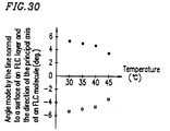
- phase transition temperature from one phase to another phase is as follows:
- the absolute value of the angles ⁇ and - ⁇ decreases in accordance with a rise in the temperature.
- the central line 103 is in substantially the same direction as the rubbing direction of the alignment layers 204a and 204b . Accordingly, in the case that the principal axis of the FLC molecules 101 in one of the two stable alignment states 104 and 105 is aligned with the polarizing axis of the polarizing plate 208a or 208b at a certain temperature, the principal axis becomes offset from the polarizing axis in accordance with a change in the temperature. Since the intensity of light transmitted through the FLC layer 207 is affected by the angle ⁇ and - ⁇ , the brightness of an image changes in accordance with a change in the temperature. Such a problem of a change in the brightness of an image in accordance with a change in the temperature is also present in the devices disclosed by Japanese Laid-Open Patent Publication Nos. 3-242624 and 3-243915.
- the circuit in Figure 16 is provided for each of a plurality of pixels in the FLCD device and includes a TFT 703 as an active element.
- the gate of the TFT 703 is connected to a gate line 701
- the source of the TFT 703 is connected to a data line 702 at 705 .
- the drain of the TFT 703 is connected to an auxiliary capacitance C S via an auxiliary electrode 706 .
- the drain is also connected to a pixel electrode 707 .
- the pixel electrode 707 and an area of a counter electrode 708 corresponding to the pixel electrode 707 with the FLC molecules sandwiched therebetween have a liquid crystal capacitance LC .
- a gate signal is sent to the gate line 701 to control the TFT 703 to be ON or OFF. While the TFT 703 is ON, image data is supplied from the data line 702 to the auxiliary capacitance C S and to the pixel electrode 707 through the TFT 703 .
- the FLC material has spontaneous polarization ( Figure 4B ).
- a voltage is applied to the FLC material, a transient current flows due to a change in the alignment orientation of the FLC molecules. Since it takes several tens to several hundreds of microseconds to change the alignment orientation of the FLC molecules, the transient current continues to flow during such a period.
- a writing time period allocated for one scanning line is several tens of microseconds or less. The transient current flows for longer than the writing time period. Due to the transient current flowing after the writing time period, the voltage applied to the FLC material changes, which prevents accurate writing.
- the field-by-field sequential color display system utilizes the limit of the time resolution of the human eye; namely, the phenomenon that, when colors are sequentially changed too fast for the human eye to recognize each change, two sequential colors are mixed and recognized as one color.
- the color of light incident on the LCD device is periodically changed, using a high speed color variable filter.
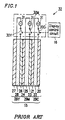
- FIG. 1 is a schematic view of a field-by-field sequential color display system 32 including a light selection device 15 .
- the light selection device 15 is used as a flat panel high speed color variable filter and is used in combination with an LCD device (not shown) including pixels for each of the RGB colors.
- the light selection device 15 includes a cyan filter 29C , a magenta filter 29M and a yellow filter 29Y laminated in this order.
- the cyan filter 29C includes two transparent substrates 20 and 21 , transparent electrodes (not shown) provided on opposed surfaces of the two transparent substrates 20 and 21 , and a liquid crystal layer 22 sandwiched between the transparent electrodes.
- the liquid crystal layer 22 includes a cyan dichroic pigment.
- the magenta filter 29M includes two transparent substrates 23 and 24 , transparent electrodes (not shown) provided on opposed surfaces of the two transparent substrates 23 and 24 , and a liquid crystal layer 25 sandwiched between the transparent electrodes.
- the liquid crystal layer 25 includes a magenta dichroic pigment.
- the yellow filter 29Y includes two transparent substrates 26 and 27 , transparent electrodes (not shown) provided on opposed surfaces of the two transparent substrates 26 and 27 , and a liquid crystal layer 28 sandwiched between the transparent electrodes.
- the liquid crystal layer 28 includes a yellow dichroic pigment.
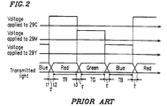
- FIG. 2 a timing diagram showing basic operation of the light selection device 15 .
- a voltage is applied to the cyan filter 29C .
- the alignment of liquid crystal molecules in the liquid crystal layer 22 are not changed immediately after the application of the voltage, but only after a certain period ⁇ .
- the period ⁇ corresponds to the response time of the liquid crystal molecules to application of the electric field. Accordingly, in the case when the application of the voltage starts at time t1, the alignment of the liquid crystal molecules in the liquid crystal layer 22 of the cyan filter 29C is stabilized at time t2.
- time t2 to time t3 namely, during time period TR, the light coming out of the light selection device 15 is red.
- Voltages are applied to the magenta filter 29M and the yellow filter 29Y in the same manner to obtain the green and blue light by the light selection device 15 .
- the color of the light incident on the LCD device can be changed periodically.
- the LCD device performs display corresponding to a red component of the data signal.
- the LCD device performs display corresponding to a green component of the data signal.
- the LCD device performs display corresponding to a blue component of the data signal.
- the human eye cannot recognize the rapid changes of the colors between red, green and blue, and so recognizes the three colors as a mixture of the colors.
- US-A-5 005 953 discloses a ferroelectric liquid crystal display device as specified in the preamble of claim 1. The device is adjusted to obtain the lowest transmissivity when the polarising axes of the two polarisers are crossed with one another. It appears that the lowest transmissivity would be achieved when the polarising axis of one of the polarisers is parallel to one of the two stable orientation directions of the ferroelectric liquid crystal molecules.
- a first aspect of the present invention provides a ferroelectric liquid crystal display device comprising:
- the ferroelectric liquid crystal molecules in one of the two stable alignment states is put at a position between the central line and a tilting axis by application of a voltage in the range between a prescribed positive voltage and a prescribed negative voltage
- the ferroelectric liquid crystal molecules in the other stable alignment state is put at a position between the central line and another tilting axis by application of a voltage in the range between another prescribed negative voltage and another prescribed positive voltage.
- the plurality of pixels are arranged in a matrix, and each of the plurality of pixels is connected to a driving circuit including:
- the plurality of pixels are arranged in a matrix, and each of the plurality of pixels is connected to a driving circuit including:
- the plurality of pixels are arranged in a matrix, and each of the plurality of pixels is connected to a driving circuit including:
- the ferroelectric liquid crystal display device further comprises two substrates sandwiching the ferroelectric liquid crystal material, and one of the two substrates is formed of single crystalline silicon and the other substrate is formed of a light-transmitting material.
- a second aspect of the present invention provides a method of driving a ferroelectric liquid crystal display device, the device including:-
- the pixels are arranged in a matrix
- the pixels are arranged in a matrix; the device further comprises:-a plurality of pixel electrodes, one pixel electrode being provided for each pixel; a single counter electrode corresponding to the plurality of pixel electrodes; and a switching means corresponding to each of the pixels;
- the device further comprises a third switching device, connected between the second switching device and the pixel for controlling an output of the charge for display sent from the second switching device to the corresponding pixel; wherein the method comprises the steps of:
- the device further comprises: a third switching device, connected between the second switching device and the pixel for controlling an output of the charge for display sent from the second switching device to the corresponding pixel, the method comprising the steps of:
- ferroelectric liquid crystal molecules in areas included in pixels included in adjacent groups of rows in the matrix are supplied with voltages having opposite polarities to each other.
- ferroelectric liquid crystal molecules in areas included in pixels included in adjacent groups of columns in the matrix are supplied with voltages having opposite polarities to each other.
- ferroelectric liquid crystal molecules in areas included in pixels included in adjacent groups of rows and columns in the matrix are supplied with voltages having opposite polarities to each other.
- ferroelectric liquid crystal molecules in areas included in adjacent pixels in the matrix are supplied with voltages having opposite polarities to each other.
- the invention described herein makes possible the advantages of providing an FLCD device which performs accurate display regardless of temperature changes, allows the same amount of light to be transmitted therethrough with respect to two voltages having the same magnitude and opposite polarities, thus to realize better display, has a high response speed and uniform alignment of the FLCD molecules, and realizes accurate display by preventing voltage fluctuation occurring due to a transient current; and provides a method for driving such an FLCD device.
- Figure 4A is a view illustrating two stable alignment states in an FLCD device seen from one of the two substrates.
- Figure 34 is a cross sectional view of an FLCD device 300 in accordance with the first example.
- Figure 24 is a graph illustrating the intensity I of light transmitted through an FLC layer 207 of the FLCD device 300 relative to the voltage V applied thereto.
- Figure 25 is a schematic diagram of the FLCD device 300 .
- Figure 26 is a waveform diagram of voltages of electrode lines and pixels in the FLCD device 300 .
- Figure 27 is a waveform diagram illustrating the relationship between the voltage V applied to the FLCD device 300 and the intensity I of light transmitted through the FLCD device 300 .
- the FLCD device 300 in accordance with the first example has a similar structure as that of the FLCD device 200 shown in Figure 20 .
- alignment layers 204a' and 204b' are treated by rubbing in the same direction (parallel rubbing) to put the FLC molecules 101 in the FLC layer 207 into one of either stable alignment state 104 or 105 as is shown in Figure 4A , and the polarizing axis of the polarizing plates 208a' or 208b' is aligned with the central line 103 with the polarizing axis of the other polarizing plate being perpendicular thereto.
- Each pixel electrode 209 , an area of the FLC layer 207 corresponding to the pixel electrode 209 , and an area of the counter electrode L also in correspondence with the pixel electrode 209 are included in a pixel.
- the FLCD device 300 is driven in the following field-by-field operation.
- a negative voltage which is equal to or lower than a negative threshold voltage -Vth is applied via the pixel electrode 209 and the counter electrode L to the FLC molecules 101 in an area of the FLC layer 207 included in a pixel to put the FLC molecules 101 into one stable alignment state 104 ( Figure 4A). Then, an arbitrary voltage in the range between a positive voltage V 1 equal to or lower than a positive threshold voltage Vth and a negative voltage -V 2 is applied to the FLC molecules 101 included in the same pixel to put the FLC molecules 101 at an arbitrary position between the central line 103 and the tilting axis 106 .
- the effective applied voltage V and the intensity I of light transmitted through the area of the FLC layer 207 included in the pixel have the relationship as is indicated by the solid line in Figure 24 .
- the threshold voltage is a minimum voltage which is necessary to move the FLC molecules 101 from one stable alignment state to the other stable alignment state.
- a positive voltage which is equal to or higher than a positive threshold voltage Vth is applied to the FLC molecules 101 included in the pixel to put the FLC molecules 101 into the other stable alignment state 105 ( Figure 4A ).
- an arbitrary voltage in the range between a negative voltage -V 1 equal to or higher than a negative threshold voltage -Vth and a positive voltage V 2 is applied to the FLC molecules 101 to put the FLC molecules 101 at an arbitrary position between the central line 103 and the tilting axis 107 .
- the effective applied voltage V and the intensity I of transmitted light have the relationship as is indicated by the dashed line in Figure 24 .
- the intensity I of transmitted light is identical with respect to two voltages having an identical absolute value and opposite polarities. Accordingly, even when the frame rate used for driving the FLCD device 300 is as low as 60 Hz, flicker is not recognized.
- the direction of the central line 103 remains substantially aligned with the rubbing direction of the polarizing plates 208a' or 208b' regardless of the temperature.
- the polarizing axis of either one of the polarizing plate 208a' or 208b' is aligned with the central line 103 , and the FLC molecules 101 are moved from the stable alignment state 104 or 105 to the central line 103 by changing the level of the voltage applied to the FLC molecules 101 .
- the FLC molecules 101 can be moved back to the stable alignment state 104 or 105 by adjusting the level of the voltage.
- the principal axis of the FLC molecules 101 when no voltage is applied is constantly oriented in the same direction regardless of the temperature.
- the FLCD device 300 utilizes bistability of the FLC material, and thus it is not necessary to realize the single stability. Further, since the darkest state is realized when a voltage equal to or greater than the threshold voltage is applied to align the principal axis of the FLC molecules 101 with the central line 103 , a uniformly aligned, satisfactory black state can be obtained. In addition, since the bistability is realized by general parallel rubbing, further satisfactory alignment and thus a higher contrast of displayed images are obtained. Moreover, as is mentioned above, the intensity of light transmitted through the FLCD device 300 is identical with respect to two voltages having an identical absolute value and opposite polarities.
- the characteristics of the FLCD device 300 are as illustrated in Figures 5 through 10 .
- Figure 5 illustrates a waveform of a voltage applied to the FLCD device 300 via the respective pixel electrodes 209 and the counter electrode L .
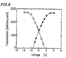
- Figure 6 is a graph illustrating the light transmission of the FLCD device 300 with respect to the voltage.
- Figure 7 is a graph illustrating the response time with respect to the voltage.
- reference numerals 801 and 802 denote pulse voltages (hereinafter, referred to as the "reset pulse voltages”) for putting the FLC molecules into two stable alignment states, respectively.
- the reset pulse voltage 801 After put into one of the two stable alignment states by the reset pulse voltage 801 , the FLC molecules 101 are put into a position corresponding to a desirable intensity of transmitted light by application of a voltage 803 .
- black circles indicate the transmission after the FLC molecules 101 are reset to one of the two stable alignment states by a positive voltage 801
- white squares indicate the transmission after the FLC molecules 101 are reset to the other stable alignment state by a negative voltage 802 .
- an image having various tones can be displayed.
- the response time is represented as the time from 10% of the total change of the intensity is obtained until 90% of the total change of the intensity is obtained or vice versa after the reset pulse voltages 801 and 802 are applied.
- black circles indicate the response time after the FLC molecules 101 are reset to one of the two stable alignment states by a positive voltage 801
- white squares indicate the response time after the FLC molecules 101 are reset to the other stable alignment state by a negative voltage 802 .
- the response speed of the FLCD device 300 is significantly higher than that of a nematic LCD device as will be appreciated.
- Figures 8 , 9 and 10 are graphs illustrating the relationship between the light transmission of the FLCD device 300 and the voltage applied thereto in a white state, an intermediate state, and a black state, respectively. Since the intensity of light is equal with respect to two voltages having an identical absolute value or magnitude and opposite polarities, flicker is not readily apparent. When a reset pulse voltage is applied, the intensity of light changes only briefly like a pulse. In the case when this FLCD device 300 is driven using, for example, a TFT, such changes cannot be visually recognized. The reason is that since the frame rate is 60 Hz; the frequency for applying reset pulse voltages is also 60 Hz, and thus the change like a pulse in the intensity of light is also generated at a frequency of 60 Hz.
- a pixel electrode 209 ( Figure 34 ) of the pixel A ij and a corresponding counter electrode L i generate an electric field.
- the orientation of the principal axis of the FLC molecules 101 is controlled by the electric field as is described above with respect to Figure 4A to obtain a desirable intensity of transmitted light.
- a single counter electrode L i acts as the counter electrode for each pixel controlled by a corresponding gate electrode line G i .
- the voltage of the counter electrode for each gate electrode line can be controlled independently.
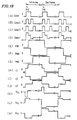
- Figure 26 is a waveform diagram of voltages applied to the electrode lines G 0 , G 1 , L 0 and L 1 , and the pixels A 00 and A 10 of the FLCD device 300 .
- the FLC material- SCE-8 produced by Merck & Co., Inc. is used; and as the alignment layers 204a' and 204b' , PSI-A-2101 produced by Chisso Petrochemical Corp. is used.
- the FLC material and the alignment layers 204a' and 204b' may be formed of any. other material which realizes bistability of the FLC molecules.
- the intensity of light transmitted through an area of the FLC layer 207 included in a pixel A 00 connected to the gate electrode line G 0 is controlled in the following manner.
- waveform ( A ) In the first field, in a period from time -t 0 to time t 0 , as is shown in waveform ( A ), an appropriate voltage is applied to the gate electrode line G 0 which is connected to the gate of a TFT B 00 , thereby activating the TFT B 00 . As is shown in waveform ( D ), in a period from time -t 0 to time 0, a positive voltage V 0 is applied to the counter electrode L 0 . Until time 0, a voltage -V b is applied to the source electrode line S 0 (waveform ( C )).
- the pixel A 00 is supplied with a voltage -V b -V 0 , which is presented to be equal to or lower than the negative threshold voltage -Vth, from time -t 0 to time 0. Accordingly, the FLC molecules 101 in an area of the FLC layer 207 included in the pixel A 00 are put into one stable alignment state 104 shown in Figure 4A .
- a voltage V b is sent from the source electrode line S 0 to the pixel A 00 , and then the TFT B 00 is turned off via the voltage provided to the gate thereof.
- the voltage V b corresponds to desired intensity I b of light transmitted through the area of the FLC layer 207 included in the pixel A 00 on the solid line in Figure 24 .
- the voltage V b is preferably in the range between the voltages -V 2 and V 1 , a voltage higher than V 1 or lower than -V 2 may also be used as the voltage V b .
- the potential of the pixel A 00 is maintained until time T 0 -t 0 , during which time the FLC molecules 101 included in the pixel A 00 are stable at a position between the central line 103 and the tilting axis 106 , the position corresponding to the voltage V b .
- the intensity Ib of light corresponding to the voltage V b on the solid line in Figure 24 is transmitted through the area of the FLC layer 207 included in the pixel A 00 .
- waveform ( A ) In the second field, in a period from time T 0 -t 0 to time T 0 +t 0 , as is shown in waveform ( A ), an appropriate voltage is applied to the gate electrode line G 0 to activate the TFT B 00 . As is shown in waveform ( D ), in a period from time T 0 -t 0 to time T 0 , a negative voltage -V 0 is applied to the counter electrode L 0 . During time 0 to time T 0 , a voltage V b is applied to the source S 0 (waveform ( C )).
- the pixel electrode A 00 is supplied with a voltage V b +V 0 , which is equal to or higher than the positive threshold voltage Vth, from time T 0 -t 0 to time T 0 . Accordingly, the FLC molecules 101 included in the pixel A 00 are put into the other stable alignment state 105 shown in Figure 4A .
- a voltage -V b is sent from the source electrode S 0 to the pixel A 00 , and then the TFT B 00 is turned off via the voltage provided to the gate thereof.
- the voltage -V b corresponds to a desired intensity of light transmitted through the area of the FLC layer 207 included in the pixel A 00 on the dashed line in Figure 24 .
- the voltage -V b is preferably in the range between the voltages -V 1 and V 2 , a voltage higher than V 2 or lower than -V 1 may also be used as the voltage -V b .
- the potential of the pixel A 00 is maintained until 2T 0 -t 0 , during which time the FLC molecules 101 included in the pixel A 00 are stable at a position between the central line 103 and the tilting axis 107 , the position corresponding to the voltage -V b .
- the intensity of light corresponding to the voltage -V b on the dashed line in Figure 24 is transmitted through the area of the FLC layer 207 included in the pixel A 00 .
- an identical intensity of light is transmitted through the area of the FLC layer 207 included in the pixel A 00 in the first field and the second field in accordance with the voltage application shown in part ( A ) of Figure 27 .
- the waveform of the intensity of the light transmitted through the pixel A 00 is repeated frame by frame. Accordingly, by setting the frame rate for driving the FLCD device 300 at 60 Hz or more, images without flicker are realized.
- the intensity of light transmitted through an area of the FLC layer 207 in correspondence with a pixel A 10 connected to a gate electrode line G 1 is controlled in the following manner.
- waveform ( B ) In the first field, in a period from time 0 to time 2t 0 , as is shown in waveform ( B ), an appropriate voltage is applied to the gate electrode line G 1 to activate a TFT B 10 connected to the gate electrode line G 1 .
- waveform ( E ) As is shown in waveform ( E ), in a period from time 0 to time t 0 , a positive voltage V 0 is applied to the counter electrode L 1 , Beginning at time 0, a voltage V b is applied to the source electrode S 0 (waveform ( C )).
- the pixel A 10 is supplied with a voltage V b -V 0 , which is equal to or less than the negative threshold voltage -Vth, from time 0 to time t 0 . Accordingly, the FLC molecules 101 included in the pixel A 10 are put into one stable alignment state 104 .
- a voltage V b is sent from the source electrode S 0 to the pixel A 10 , and then the TFT B 10 is turned off.
- the voltage V b corresponds to a desired intensity of light transmitted through an area of the FLC layer 207 included in the pixel A 10 on the solid line in Figure 24 .
- the voltage V b is preferably in the range between the voltages -V 2 and V 1 , a voltage higher than V 1 or lower than -V 2 may also be used as the voltage V b .
- the potential of the pixel A 10 is maintained until T 0 , during which time the FLC molecules 101 included in the pixel A 10 are stable at a position between the central line 103 and the tilting axis 106 , the position corresponding to the voltage V b .
- the intensity I b of light corresponding to the voltage V b on the solid line in Figure 24 is transmitted through the area of the FLC layer 207 included in the pixel A 10 .
- waveform ( B ) In the second field, in a period from time T 0 to time T 0 +2t 0 , as is shown in waveform ( B ), an appropriate voltage is applied to the gate electrode line G 1 to activate the TFT B 10 . As is shown in waveform ( E ), in a period from time T 0 to time T 0 +t 0 , a negative voltage -V 0 is applied to the counter electrode L 1 . Beginning at time T 0 , a voltage -V b is applied to the source electrode S 0 (waveform ( C )).
- the pixel A 10 is supplied with a voltage -V b +V 0 , which is equal to or higher than the positive threshold voltage Vth from time T 0 to time T 0 +t 0 . Accordingly, the FLC molecules 101 included in the pixel A 10 are put into the other stable alignment state 105 .
- a voltage -V b is sent from the source electrode line S 0 to the pixel A 10 , and then the TFT B 10 is turned off via the voltage provided to the gate thereof.
- the voltage -V b corresponds to a desired intensity of light transmitted through the area of the FLC layer 207 included in the pixel A 10 on the dashed line in Figure 24 .
- the voltage -V b is preferably in the range between the voltages -V 1 and V 2 , a voltage higher than V 2 or lower than -V 1 may also be used as the voltage -V b .
- the potential of the pixel A 10 is maintained until 2T 0 , during which time the FLC molecules 101 included in the pixel A 10 are stable at a position between the central line 103 and the tilting axis 107 , the position corresponding to the voltage -V b .
- the intensity of light corresponding to the voltage -V b on the dashed line in Figure 24 is transmitted through the area of the FLC layer 207 included in the pixel A 10 .
- an identical intensity of light is transmitted through the area of the FLC layer 207 included in the pixel A 10 in the first field and the second field in accordance with the voltage application shown in part ( A ) of Figure 27 .
- the waveform of the intensity of the light transmitted through the pixel A 10 is repeated frame by frame. Accordingly, by setting the frame rate for driving the FLCD device 300 at 60 Hz or more, images without flicker are realized. The driving is performed in the same manner at the other pixels A ij .
- the voltage shown in part ( A ) of Figure 27 is the same as the voltage shown in part ( F ) of Figure 26 .
- a positive voltage V 0 is applied in a period from time -t 0 to time 0 (waveform ( D )) in the above-described example
- a voltage V b -V 0 may be applied directly to the source electrode line S 0 while maintaining the potential of the counter electrode L at 0, i.e., while using the potential of the counter electrode L as a reference potential.
- a voltage V b -V 0 may be applied directly to the counter electrode L while maintaining the potential of the pixel electrode A ij at 0, namely, while using the potential of the pixel electrode A ij as a reference potential.
- Figure 28 is a waveform diagram of voltages applied to the electrode lines G 0 , G 1 , L 0 and L 1 , and the pixels A 00 and A 10 of the FLCD device 300 .
- the pixels for example A 0j and A 2j connected to the even numbered gate electrode lines, for example, G 0 and G 2
- the pixels for example, A 1j and A 3j connected to the odd numbered gate electrodes, for example, G 1j and G 3j are supplied with voltages having opposite polarities to each other.
- the polarity of the voltage applied to the source electrode line S 0 is inverted alternately line by line, e.g., the voltage has one polarity with respect to even numbered gate electrode lines and an opposite polarity with respect to odd numbered gate electrode lines.
- the pixel A 00 connected to the even numbered gate electrode line G 0 and the pixel A 10 connected to the odd numbered gate electrode line G 1 are supplied with voltages having opposite polarities to each other.
- the intensity of light transmitted through an area of the FLC layer 207 included in each pixel changes frame by frame.
- the voltage applied to the source electrode line S j and the counter electrode L i is shifted by -V 1 (or a level close to -V 1 ) to put the FLC molecules 101 into the other stable alignment state 105 .
- the voltage applied to the source electrode line S j and the counter electrode L i is shifted by V 1 (or a level close to V 1 ).
- the voltage applied to the pixel A ij is identical with the voltage applied by the above-described system.
- the FLCD device 300 does not have a counter electrode line L i for each gate electrode line G i , but has only a single counter electrode L for all the gate electrode lines.
- the voltage V ij retained in the pixel A ij is determined by Equation (1) based on the charge Q ij retained in the pixel A ij and the capacitance C ij of the pixel Aij.
- V ij Q ij /C ij Accordingly, the voltage V ij retained in the pixel A ij having a TFT which is in an OFF state does not change even if the voltage applied to the counter electrode L is changed to, for example, V 0 .
- the FLCD device 300 is driven in the following manner in accordance with the third example.
- Figure 29 is a waveform diagram applied to the electrode lines and the pixels of the FLCD device 300 in accordance with the third example.
- waveform ( A ) in a period from time -to to time t 0 , an appropriate voltage is applied to the gate of the TFT B 00 connected to the gate electrode line G 0 , thereby activating the TFT B 00 .
- waveform ( D ) in a period from time -to to time 0, a positive voltage V 0 is applied to the counter electrode L .
- a voltage V b is applied to the source electrode line S 0 (waveform ( C )).
- the pixel A 00 is supplied from time -t 0 to time 0 with a voltage -V b -V 0 , which is equal to or lower than the negative threshold voltage -Vth 0. Accordingly, the FLC molecules 101 in an area of the FLC layer 207 included in the pixel A 00 are put into one stable alignment state 104 shown in Figure 4A .
- a voltage V b is sent from the source electrode line S 0 to the pixel A 00 , and then the TFT B 00 is turned off via the voltage applied to the gate thereof.
- the potential of the pixel A 00 is then maintained until time T 0 -t 0 , during which time the FLC molecules 101 included in the pixel A 00 are stable at a position between the central line 103 and the tilting axis 106 , the position corresponding to the voltage V b .
- a positive voltage V 0 is applied in a period from time -t 0 to time 0 (waveform ( D )) in the above-described example
- a voltage V b -V 0 may be applied directly to the source electrode line S 0 while maintaining the potential of the counter electrode L at 0, i.e., while using the potential of the counter electrode L as a reference potential.
- a voltage V b -V 0 may be applied directly to the counter electrode L while maintaining the potential of the pixel electrode A 00 at 0, namely, while using the potential of the pixel electrode A 00 as a reference potential.
- waveform ( A ) in a period from time T 0 -t 0 to time T 0 +t 0 , an appropriate voltage is applied to the gate electrode line G 0 to activate the TFT B 00 connected to the gate electrode line G 0 .
- waveform ( D ) in a period from time T 0 -t 0 to time T 0 , a negative voltage -V 0 is applied to the counter electrode L .
- a voltage -V b is applied to the source electrode line S 0 (waveform ( C )).
- the pixel A 00 is supplied with a voltage -V b +V 0 , which is equal to or higher than the positive threshold voltage Vth from time T 0 -t 0 to time T 0 . Accordingly, the FLC molecules 101 included in the pixel A 00 are put into the other stable alignment state 105 shown in Figure 4A .
- a voltage -V b is sent from the source electrode line S 0 to the pixel A 00 , and the TFT B 00 is turned off via the voltage provided to the gate thereof.
- the potential of the pixel A 00 is maintained until time 2T 0 -t 0 , during which time the FLC molecules 101 included in the pixel A 00 are stable at a position between the central line 103 and the tilting axis 107 , the position corresponding to the voltage -V b .
- a negative voltage -V 0 is applied in a period from time until T 0 -t 0 to time T 0 (waveform ( D )) in the above-described example, a voltage -V b +V 0 may be applied directly to the source electrode line S 0 while maintaining the potential of the counter electrode L at 0.
- the pixels A 1j connected to the gate electrode line G 1 are driven in the following manner.
- waveform ( B ) in a period from time t 0 to time 3t 0 , an appropriate voltage is applied to the gate electrode line G 1 to activate the TFT B 10 connected to the gate electrode line G 1 .
- waveform ( D ) in a period from time t 0 to time 2t 0 , a positive voltage V 0 is applied to the counter electrode L .
- waveform ( F ) the pixel A 10 is supplied with a voltage V b -V 0 , which is equal to or lower than the negative threshold voltage -Vth. Accordingly, the FLC molecules 101 included in the pixel A 10 are put into one stable alignment state 104 .
- a voltage V b is sent from the source electrode line S 0 to the pixel A 10 , and then the TFT B 10 is turned off.
- the potential of the pixel A 10 is maintained until T 0 +t 0 , during which time the FLC molecules 101 included in the pixel A 10 are stable at a position between the central line 103 and the tilting axis 106 , the position corresponding to the voltage V b .
- a positive voltage V 0 is applied in a period from time t 0 to time 2t 0 (waveform ( D )) in the above-described example, a voltage -V b +V 0 may be applied directly to the source electrode line S 0 while maintaining the potential of the counter electrode L at 0.
- waveform ( B ) in a period from time T 0 +t 0 to time T 0 +3t 0 , an appropriate voltage is applied to the gate electrode line G 1 to activate the TFT B 10 connected to the gate electrode line G 1 .
- waveform ( D ) in a period from time T 0 +t 0 to time T 0 +2t 0 , a negative voltage -V 0 is applied to the counter electrode L .
- waveform ( F ) the pixel A 10 is supplied with a voltage -V b +V 0 , which is equal to or higher than the positive threshold voltage Vth. Accordingly, the FLC molecules 101 included in the pixel A 10 are put into the other stable alignment state 105 .
- a voltage -V b is sent from the source electrode line S 0 to the pixel A 10 , and then the TFT B 10 is turned off.
- the potential of the pixel A 10 is maintained until 2T 0 +t 0 , during which time the FLC molecules 101 included in the pixel A 10 are stabilized at a position between the central line 103 and the tilting axis 107 , the position corresponding to the voltage -V b .
- a negative voltage -V 0 is applied in a period from time T 0 +t 0 to time T 0 +2t 0 (waveform ( D )) in the above-described example, a voltage -V b +V 0 may be applied directly to the source electrode line S 0 while maintaining the potential of the counter electrode L at 0.
- the FLCD device 300 is driven by a plane-scanning active matrix driving circuit for field-by-field sequential color display.
- Figure 31 is a circuit diagram of such an active driving circuit, which is provided for each of the pixels located at the intersections of the gate electrode lines G i and the source electrode lines S j shown in Figure 25 .
- a plane-scanning gate electrode F Gate is common to all the pixels A ij in the FLCD device 300 .
- Figure 32 is a waveform diagram of voltages applied to the electrode lines and the pixels in the FLCD device 300 having the active driving circuit.
- the FLCD device operates in the following manner in accordance with the fourth example.
- a potential stored in capacitors C S each connected to a corresponding pixel A ij is sent to the pixel A ij having a liquid crystal capacitance LC .
- the color of the light transmitted through the areas of the FLC layer 207 included in all the pixels A ij is made blue.
- the voltage applied to the counter electrode L is changed to 0 V at time -t 0 .
- the potential of all the pixels A ij is maintained until an appropriate voltage is applied to the plane-scanning gate electrode line F Gate to activate all the TFTs Q3 ij .
- the FLC molecules 101 included in all the pixels A ij are stable at a position between the central line 103 and the tilting axis 106 , the position corresponding to the voltage -V b .
- the intensity of light corresponding to the voltage -V b on the solid line in Figure 24 is transmitted through the areas of the FLC layer 207 included in all the pixels A ij .
- an appropriate voltage is applied to a gate electrode line G 0 to activate a TFT Q1 0j as an active element connected to the gate electrode line G 0 .
- a voltage V b is sent from the source electrode line S j to the capacitor C S connected to a pixel A 0j , and then the TFT Q1 0j is turned off.
- the voltage V b corresponds to a desired intensity of light transmitted through an area of the FLC layer 207 included in the pixel A 0j on the dashed line in Figure 24 .
- an appropriate voltage is applied to a gate electrode line G 1 to activate a TFT Q1 1j as an active element connected to the gate electrode line G 1 .
- a voltage V b is sent from the source electrode S j to the capacitor C S connected to a pixel A 1j , and then the TFT Q1 1j is turned off.
- the voltage V b corresponds to a desired intensity of light transmitted through an area of the FLC layer 207 included in the pixel A 1j on the dashed line in Figure 24 .
- capacitors C S connected to the other pixels A ij are supplied with voltages. Then, in a period from time T 0 -2t 0 to time T 0 , as is shown in waveform (D) , an appropriate voltage is applied to the plane-scanning gate electrode line F Gate to activate all the TFTs Q3 ij .
- the voltage applied to the counter electrode L is charged to 0 V at time T 0 -t 0 .
- the potential of all the pixels A ij is maintained until an appropriate voltage is applied to the plane-scanning gate electrode line F Gate to activate all the TFTs Q3 ij .
- the FLC molecules 101 included in all the pixels A ij are stable at a position between the central line 103 and the tilting axis 107 , the position corresponding to the voltage V b .
- the intensity I b of light corresponding to the voltage V b on the dashed line in Figure 24 is transmitted through the areas of the FLC layer 207 included in all the pixels A ij .
- an appropriate voltage is applied to the gate electrode line G 0 to activate the TFT Q1 0j connected to the gate electrode line G 0 .
- a voltage -V b is sent from the source electrode line S j to the capacitor C S connected to the pixel A 0j , and then the TFT Q1 0j is turned off.
- the voltage -V b corresponds to a desired intensity of light transmitted through an area of the FLC layer 207 included in the pixel A 0j on the dashed line in Figure 24 .
- an appropriate voltage is applied to the gate electrode line G 1 to active the TFT Q1 1j connected to the gate electrode line G 1 .
- a voltage -V b is sent from the source electrode line S j to the capacitor C S connected to the pixel A 1j , and then the TFT Q1 1j is turned off.
- the voltage -V b corresponds to a desired intensity of light transmitted through the area of the FLC layer 207 included in the pixel A 1j on the solid line in Figure 24 .
- capacitors C S connected to the other pixels A ij are supplied with voltages. Then, in a period from time 2T 0 -2t 0 to time 2T 0 , as is shown in waveform ( D ), an appropriate voltage is applied to the plane-scanning gate electrode line F Gate to activate all the TFTs Q3 ij .
- a potential stored in the capacitors C S each connected to a corresponding pixel A ij is sent to the pixel A ij having the liquid crystal capacitance LC .
- the color of the light transmitted through the areas of the FLC layer 207 included in all the pixels A ij is made green.
- the voltage applied to the counter electrode L is changed to 0 V at time 2T 0 -t 0 .
- the potential of all the pixels A ij is maintained until an appropriate voltage is applied to the plane-scanning gate electrode line F Gate to activate all the TFTs Q3 ij .
- the FLC molecules 101 included in all the pixels A ij are stable at a position between the central line 103 and the tilting axis 106, the position corresponding to the voltage -V b .
- the intensity of light corresponding to the voltage -V b on the solid line in Figure 24 is transmitted through the areas of the FLC layer 207 included in all the pixels A ij .
- the above-described scanning operation is repeated in the order of blue, red and green.
- the potential of all the pixels A ij in the FLCD device 300 can be simultaneously updated.
- the potential for display can be transferred to all the pixels A ij during time period ⁇ ( Figure 2 ) in which the light colors are changed. Accordingly, rays of each color of light are transmitted even while line-by-line sequential scanning is performed. Therefore, high speed field-by-field sequential color display system is realized.
- an LCD device having a response time of 1/180 second is required.
- an FLCD device allows sufficiently high speed operation to be used for such a field-by-field sequential color display system. Accordingly, by the FLCD device and the driving method in accordance with the fourth example, the intensity of transmitted light changes frame by frame, and field-by-field sequential color display is realized by displaying images corresponding to all the RGB colors within 1/60 second.
- Figure 33 shows a circuit for driving the FLCD device 300 which is further improved from the circuit shown in Figure 31 .
- the circuit in Figure 33 includes another charge retaining capacitance C F connected to the third transistor Q3 and a fourth transistor Q4 for sending a charge from an additional power source to the pixel A ij having the liquid crystal capacitance LC in addition to the structure of the circuit shown in Figure 31 .
- the method for driving the circuit shown in Figure 33 is the same as the method for driving the circuit shown in Figure 31 until activating the TFT Q 3 .
- a charge is sent to a capacitance C F from the power source, thereby activating a TFT Q 4 .
- a charge from an additional (second) power source is sent to the pixel A ij having the liquid crystal capacitance LC to realize display.
- the intensity of transmitted light changes frame by frame
- a frequency conversion circuit is not necessary between the FLCD device and a signal source such as a computer.
- the production cost of a system including the FLCD device is reduced while reducing flicker.
- LCD devices including the amorphous silicon TFT is not suitable for an apparatus requiring a large capacity display such as a high definition TV. Because of the high ON/OFF ratio of the current, it is difficult to use an amorphous silicon TFT for a complicated circuit such as a driving circuit formed on the same substrate with the display area using known IC production technologies.
- a polysilicon TFT is sufficiently satisfactory in performance to be used in a complicated circuit such as driving circuit formed on the same substrate with the display area using known IC production technologies. Nonetheless, since the polysilicon TFT has a large current leakage, it is necessary that the TFT should be increased in size or a plurality of TFTs should be connected in series in order to raise the ON/OFF ratio of the current. Such increase in size contradicts the size reduction of the LCD device, which is demanded today.
- a TFT is formed in a substrate formed of single crystalline silicon. As is indicated in Table 3, such a TFT has a large driving capacity and a high ON/OFF ratio of the current without increasing the size of the TFT.
- a circuit having a plurality of active elements and capacitors can be configurated.
- An FLCD device including such a circuit can realize functions which cannot be achieved by use of conventional TFTs.
- the FLCD device includes a base substrate 1 formed of p-type single crystalline silicon. On the base substrate 1 , an NMOS switching circuit is mounted.
- the pixel area includes a first transistor Q1 and a second transistor Q2 .
- a source region Q1s of the first transistor Q1 and a source region Q2s of the second transistor Q2 and a drain region Q1d of the first transistor Q1 and a drain region Q2d of the second transistor Q2 are each formed as an n-type diffusion layer 2 in the p-type base substrate 1 .
- a gate electrode Q1g of the first transistor Q1 is provided above the base substrate 1 to be partially superposed on the source region Q1s and the drain region Q1d and is entirely covered with a gate insulation layer 3g .
- a gate electrode Q2g of the second transistor Q1 is provided above the base substrate 1 to be partially superposed on the source region Q2s and the drain region Q2d and is entirely covered with a gate insulation layer 3g .
- the gate electrodes Q1g and Q2g are formed of polysilicon, and the gate insulation layer 3g is formed of silicon oxide.
- the gate electrodes Q1g and Q2g are isolated from each other by a silicon oxide film 6 and an aluminum electrode 7a .
- the pixel area further includes an auxiliary capacitance C S includes a polysilicon electrode 7c provided in the silicon oxide film 6 , an n-type diffusion layer 17 provided in the base substrate 1 in positional correspondence with the polysilicon electrode 7c , and a gate oxide layer 18 sandwiched between the polysilicon electrode 7c and the n-type diffusion layer 17 .
- the drain region Q1d of the first transistor Q1 , the gate electrode Q2g of the second transistor Q2 and the polysilicon electrode 7c of the auxiliary capacitance C S are all connected to an aluminum wire 7b provided on the silicon oxide film 6 ( Figure 11 ).
- the aluminum electrode 7a provided between the second transistor Q2 and the silicon oxide film 6 and partially extended onto the silicon oxide film 6 .
- the protective film 8 has a through-hole 9 at a position corresponding to such an extended area of the aluminum electrode 7a .
- a pixel electrode 10 is provided on a certain area on the protective film 8 .
- the pixel electrode 10 is connected to the aluminum electrode 7a via the through-hole 9 , and is further connected to the drain region Q2d of the second transistor Q2 via the aluminum electrode 7a .
- the gate electrode Q1g of the first transistor Q1 is connected to a scanning line 4
- the source region Q1s of the first transistor Q1 is connected to a signal line 5 which crosses the scanning line 4 .
- a glass substrate 11 is located to be opposed to the base substrate 1 .
- a surface of the glass substrate 11 is entirely covered with a counter electrode 12 .
- the counter electrode 12 and the pixel electrode 10 are both covered with an alignment film.
- An FLC layer 13 is sandwiched between the alignment films. Light is incident on the substrate 11 .
- the pixel electrode 10 which also acts as a reflection film, should be thermally treated in order to reduce the contact resistance between the pixel electrode 10 and the aluminum electrode 7a acting as a lower electrode.
- a surface of the pixel electrode 10 becomes rugged, and as a result, the reflection ratio is lowered.
- a surface of the protective film 8 is smoothed by polishing, and the surface of the pixel electrode 10 is smoothed by polishing after thermal treatment thereof.
- Such smoothing steps contribute to improvement in the alignment of the FLC molecules. Since the FLC molecules are especially difficult to be aligned and are liable to generate defects even due to microscopic ruggedness, the smoothing steps of the pixel electrode 10 is effective in realizing satisfactory alignment.
- the FLC molecules can be stable in the two stable alignment states ( Figure 4A ), and the polarizing axis of one of the polarizers is aligned with the central line 103 .
- the FLCD device 100 realizes the same effects as those of the FLCD device 300 described in the first example.
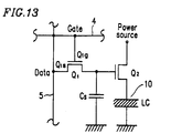
- Figure 13 is a circuit diagram or a circuit for driving the FLCD device 100 shown in Figures 11 and 12 .
- the circuit configuration shown in Figure 13 is provided for each pixel area.
- the first transistor Q1 is connected to the scanning line 4 and to the signal line 5 .
- the drain region Q1d of the first transistor Q1 is connected to an end of the auxiliary capacitance C S , and the second transistor Q2 is connected to a power source and to the pixel electrode 10 .
- the second transistor Q2 is provided for applying a voltage to the FLC layer 13 .
- the potential of the gate electrode Q2g and the potential of the drain region Q2d preferably have substantially a linear relationship.
- the second transistors Q2 need to have a withstand voltage required for switching the states of the FLC molecules in the FLC layer 13 since the second transistor Q2 directly applies a voltage to the FLC layer 13 .
- the first transistor Q1 is provided for sending a data signal to the second transistor Q2 .
- the first transistor Q1 preferably has a low current leakage in an OFF state.
- the auxiliary capacitance C S is provided for retaining the data signal sent to the second transistor Q2 .
- the data signal is sent to the second transistor Q2 .
- the data signal is retained in the auxiliary capacitance C S .
- the second transistor Q2 applies a voltage corresponding to the data signal to the FLC layer 13 to change the alignment of the FLC molecules.
- the ON state of the second transistor Q2 is maintained even after the first transistor Q1 is turned OFF. Accordingly, when the switching circuit in the fifth example is used, high quality display is obtained even if the liquid crystal material has a high resistance and a large spontaneous polarization.
- a data signal is retained in the auxiliary capacitance C S , and the potential across the auxiliary capacitance C S is provided to the gate electrode Q2g of the second transistor Q2 .
- the pixel electrode 10 is connected to the drain region Q2d of the second transistor Q2 .
- the charge which is consumed by a change in the spontaneous polarization of the FLC molecules is supplied from the power source via the source region Q2s .
- the charge retained in the auxiliary capacitance C S connected to the gate electrode Q2g is not consumed almost at all. Therefore, the voltage applied to the FLC molecules is not changed.
- the level of the charge retained in the auxiliary capacitance C S can be lower than that of the charge retained in the liquid crystal capacitance LC . Therefore, the level of the charge transferred via the source region Q2s is reduced, and thus the period of time in which the first TFT Q1 is ON can be shortened.
- the circuit shown in Figure 13 may further include an additional transistor or other devices for any specific need. Even if an FLCD device including an amorphous silicon TFT or a polysilicon TFT instead of using a base substrate formed of single crystalline silicon can realize high speed operation by reducing the level of the auxiliary capacitance C S . Such an FLCD device is included in the scope of the present invention.
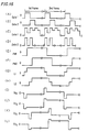
- Figure 14 is a block diagram of a circuit for driving the FLCD device 100 .
- Figure 15 is a waveform diagram of voltages applied to elements of the FLCD device 100 .
- P 1/1 , P 1/2 , P 2/1 , and P 2/2 indicate pixels formed on the base substrate 1 .
- Each pixel has a driving circuit.
- the FLCD device 100 includes any required number of scanning lines and signal lines in actuality.
- a plurality of gate lines (only Gate 1 and Gate 2 are shown in Figure 14 ; each corresponding to the scanning line 4 shown in Figure 11 ) running in a row direction parallel to each other, and a plurality of data lines (only Data 1 and Data 2 are shown in Figure 14 ; each corresponding to the signal line 5 shown in Figure 11 ) running in a column direction parallel to each other are provided.
- the gate lines are provided for supplying a gate signal, and the data lines are provided for supplying a data signal.
- a plurality of power source lines (only PW1 and PW2 are shown in Figure 14 for simplicity) each for supplying a power are provided parallel to the gate lines.
- a plurality of counter voltage lines (only L1 and L2 are shown in Figure 15 for simplicity) each for supplying a counter voltage are provided parallel to the data lines.
- a voltage of 6 V is applied to the gate line Gate 1 .
- a signal is applied to the data lines, for example, Data 1 and Data 2 (waveforms ( C ) and ( D )) to activate the second transistor Q2 .
- the power source line PW1 is supplied with a negative voltage (waveform ( E ))
- the counter voltage line L1 is supplied with a voltage of 0 V (waveform ( G )).
- the second transistor Q2 is fully activated to apply a sufficiently high negative voltage from the power source line PW1 to areas of the FLC layer 13 in correspondence with the gate line Gate 1 .
- the FLC molecules in the areas are put into one of two stable alignment states.
- a data signal is sent to the data lines, for example, Data 1 and Data 2 (waveforms ( C ) and ( D )) to supply a signal to the corresponding pixels.
- the data signal has a positive value.
- display data for the first row is written in the pixels (for example, the pixels P 1/2 and P 1/2 ).
- the power source line PW1 is supplied with a positive voltage (waveform (E))
- the counter voltage line L1 is supplied with a positive voltage having a prescribed value (waveform (G)).
- the above-mentioned areas of FLC layer 13 are supplied with a voltage having a level corresponding to the difference between the voltage sent from the power source line PW1 through the second transistor Q2 and the voltage from the counter voltage line L1 .
- the data signal is maintained in the auxiliary capacitance C S , and the power source line PW1 and the counter voltage line L1 are still supplied with a voltage (waveforms (E) and (G)) .
- the above-mentioned areas of the FLC layer 13 are still supplied with a voltage having an identical level with that of the voltage supplied immediately before the gate line Gate 1 turns OFF.
- the pixels P 1/1 and P 1/2 are respectively supplied with voltages V 1/1 and V 1/2 (waveforms (I) and (J)) .
- V 1/1 and V 1/2 waveforms (I) and (J)
- a voltage of 6 V is applied to the gate lines in the above-mentioned example, a different level of voltage can be used depending on the polarity of the power source.
- the second transistor Q2 is fully activated to apply a sufficiently high negative voltage from the power source line PW2 to areas of the FLC layer 13 in correspondence with the gate line Gate 2 .
- the FLC molecules in the areas are put into the one of the two stable alignment states.
- a data signal is sent to the data lines, for example, Data 1 and Data 2 (waveforms ( C ) and ( D )) to supply a signal to the corresponding pixels.
- the data signal has a positive value.
- display data for the second row is written in the pixels (for example, the pixels P 2/1 and P 2/2 ).
- the power source line PW2 is supplied with a positive voltage (waveform ( F )), and the counter voltage line L2 is supplied with a positive voltage having a prescribed value (waveform ( H )).
- the above-mentioned areas of the FLC layer 13 are supplied with a voltage having a level corresponding to the difference between the voltage sent from the power source line PW2 through the second transistor Q2 and the voltage from the counter voltage line L2 .
- the gate line Gate 2 turns OFF, the data signal is maintained in the auxiliary capacitance C S , and the power source line PW2 and the counter voltage line L2 are still supplied with a voltage (waveforms ( F ) and ( H )).
- the above-mentioned areas of the FLC layer 13 are still supplied with a voltage having an identical level with that of the voltage supplied immediately before the gate line Gate 2 turns OFF.
- the pixels P 2/1 and P 2/2 are respectively supplied with voltages V 2/1 and V 2/2 (waveforms ( K ) and ( L )).
- a voltage of 6 V is applied to the gate lines in the above-mentioned example, a different level of voltage can be used depending on the polarity of the power source.
- the above-described operation is repeated during the first frame to write data required for the first frame.
- the power source lines PW1 and PW2 and the counter voltage lines L1 and L2 are each supplied with a voltage having an opposite polarity to that of the voltage applied in the first frame.
- the FLC layer 13 is supplied with positive and negative voltages by the same number.
- the second transistor Q2 keeps on applying the voltage in accordance with the data signal retained in the auxiliary capacitance C S to the FLC layer 13 until the first transistor Q1 turns ON again. Such operation avoids the change in the voltage applied to the FLC layer 13 caused by the transient current. Thus, accurate display is realized.
- a data signal is sent to the data line Data 1 (waveform ( D )) to supply a signal to a corresponding pixel.
- the data signal has a positive value.
- display data for the first row is written in the pixels (for example, the pixel P 1/1 ).
- the power source line PW1 is supplied with a positive voltage (waveform (E))
- the counter voltage line L1 is supplied with a positive voltage having a prescribed value (waveform ( H )).
- the above-mentioned areas of FLC layer 13 are supplied with a voltage having a level corresponding to the difference between the voltage sent from the power source line PW1 through the second transistor Q2 and the voltage from the counter voltage line L1 .
- the data signal is maintained in the auxiliary capacitance C S , and the power source line PW1 and the counter voltage line L1 are still supplied with a voltage (waveforms ( E ) and ( H )).
- the above-mentioned areas of the FLC layer 13 are still supplied with a voltage having an identical level with that of the voltage supplied immediately before the gate line Gate 1 turns OFF.
- the pixel P 1/1 is supplied with a voltage V 1/1 (waveform ( K )).
- V 1/1 waveform ( K )
- a voltage of 6 V is applied to the gate lines in the above-mentioned example, a different level of voltage can be used depending on the polarity of the power source.
- the gate line Gate 2 is turned ON by applying a voltage of 6 V (waveform ( B )).
- a signal is applied to the data line Data 1 (waveform ( D )) to activate the second transistor Q2 .
- the power source line PW2 is supplied with a negative voltage (waveform ( F ))
- the counter voltage line L2 is supplied with a voltage of 0 V (waveform ( I )).
- the second transistor Q2 is fully activated to apply a sufficiently high positive voltage sent from the power source line PW2 to areas of the FLC layer 13 in correspondence with the gate line Gate 2 .
- the FLC molecules in the areas are put into the other of the two stable alignment states.
- a data signal is sent to the data line Data 1 (waveform ( D )) to supply a signal to a corresponding pixel.
- the data signal has a positive value.
- display data for the second row is written in the pixels (for example, the pixel P 2/1 ).
- the power source line PW2 is supplied with a negative voltage (waveform ( F )), and the counter voltage line L2 is supplied with a negative voltage having a prescribed value (waveform ( I )).
- the above-mentioned areas of the FLC layer 13 are supplied with a voltage having a level corresponding to the difference between the voltage sent from the power source line PW2 through the second transistor Q2 and the voltage from the counter voltage line L2 .
- the data signal is maintained in the auxiliary capacitance C S , and the power source line PW2 and the counter voltage line L2 are still supplied with a voltage (waveforms ( F ) and ( I )).
- the above-mentioned areas of the FLC layer 13 are still supplied with a voltage having an identical level with that of the voltage supplied immediately before the gate line Gate 2 turns OFF.
- the pixel P 2/1 is supplied with a voltage V 2/1 (waveform ( L )).
- V 2/1 waveform ( L )
- a voltage of 6 V is applied to the gate lines in the above-mentioned example, a different level of voltage can be used depending on the polarity of the power source.
- the gate line Gate 3 is turned ON by applying a voltage of 6 V (waveform ( C )).
- a signal is applied to the data line Data 1 (waveform ( D )) to activate the second transistor Q2 .
- a power source line PW3 is supplied with a negative voltage (waveform ( G ))
- a counter voltage line L3 is supplied with a voltage of 0 V (waveform ( J )).
- the second transistor Q2 is fully activated to apply a sufficiently high negative voltage from the power source line PW3 to areas of the FLC layer 13 in correspondence with the gate line Gate 3 .
- the FLC molecules in the areas are put into one of the two stable alignment states.
- This stable alignment state is the same as that obtained after the gate line Gate 3 turned ON.
- a data signal is sent to the data line Data 1 (waveform ( D )) to supply a signal to a corresponding pixel.
- the data signal has a positive value.
- display data for the third row is written in the pixels (for example, a pixel P 3/1 although not shown).
- the power source line PW3 is supplied with a positive voltage (waveform ( G )), and the counter voltage line L3 is supplied with a positive voltage having a prescribed value (waveform ( J )).
- the above-mentioned areas of the FLC layer 13 are supplied with a voltage having a level corresponding to the difference between the voltage sent from the power source line PW3 through the second transistor Q2 and the voltage from the counter voltage line L3 .
- the data signal is maintained in the auxiliary capacitance C S , and the power source line PW3 and the counter voltage line L3 are still supplied with a voltage (waveforms ( G ) and ( J )).
- the above-mentioned areas of the FLC layer 13 are still supplied with a voltage having an identical level with that of the voltage supplied immediately before the gate line Gate 3 turns OFF.
- the pixel P 3/1 is supplied with a voltage V 3/1 (waveform ( M )).
- V 3/1 waveform ( M )
- a voltage of 6 V is applied to the gate lines in the above-mentioned example, a different level of voltage can be used depending on the polarity of the power source.
- the above-described operation is repeated during the first frame to write data required for the first frame.
- the power source lines for example, PW1 , PW2 and PW3 and the counter voltage lines, for example, L1 , L2 and L3 are each supplied with a voltage having an opposite polarity to that of the voltage applied in the first frame.
- the FLC layer 13 is supplied with positive and negative voltages by the same number. Adjacent areas of the FLC layer 13 are supplied with voltages having opposite polarities to each other to be put into one of the two stable alignment states.
- a reset voltage is applied to all the pixels at the start or the end of a frame, thereby putting the FLC molecules in all the pixels into one of the two stable states.
- a voltage of 6 V is applied to all the gate lines, for example, Gate 1 , Gate 2 and Gate 3 (waveforms ( A ), ( B ) and ( C )).
- a signal is applied to all the data lines, for example, Data 1 (waveform ( D )) to activate the second transistors Q2 .
- all the power source lines for example, PW1 , PW2 and PW3 are supplied with a negative voltage (waveforms ( E ), ( F ) and ( G )), and all the counter voltage lines, for example, L1 , L2 and L3 are supplied with a voltage of 0 V (waveforms ( H ), ( I ) and ( J )).
- the second transistor Q2 is fully activated to apply a sufficiently high negative voltage from all the power source lines to areas of the FLC layer 13 in correspondence all the gate lines.
- the FLC molecules in the areas are put into one of the two stable alignment states.
- the gate line Gate 1 is kept ON by a voltage application of 6 V (waveform ( A )).
- a data signal is sent to the data line Data 1 (waveform ( D )) to supply a signal to a corresponding pixel.
- the data signal has a positive value.
- display data for the first row is written in the pixels (for example, the pixel P 1/1 ).
- the power source line PW1 is supplied with a positive voltage (waveform ( E ))
- the counter voltage line L1 is supplied with a positive voltage having a prescribed value (waveform ( H )).
- the areas of FLC layer 13 in correspondence with the gate line Gate 1 are supplied with a voltage having a level corresponding to the difference between the voltage sent from the power source line PW1 through the second transistor Q2 and the voltage from the counter voltage line L1 .
- the data signal is maintained in the auxiliary capacitance C S , and the power source line PW1 and the counter voltage line L1 are still supplied with a voltage (waveforms ( E ) and ( H )).
- the areas of the FLC layer 13 in correspondence with the gate line Gate 1 are still supplied with a voltage having an identical level with that of the voltage supplied immediately before the gate line Gate 1 turns OFF.
- the pixel P 1/1 is supplied with a voltage V 1/1 (waveform ( K )).
- V 1/1 waveform ( K )
- a voltage of 6 V is applied to the gate lines in the above-mentioned example, a different level of voltage can be used depending on the polarity of the power source.
- the gate line Gate 2 is turned ON by applying a voltage of 6 V (waveform ( B )).
- a data signal is applied to the data line Data 1 (waveform ( D )) to supply a signal to a corresponding pixel.
- the data signal has a positive value.
- display data for the second row is written in the pixels (for example, the pixel P 2/1 ).
- the power source line PW2 is supplied with a positive voltage (waveform ( F )), and the counter voltage line L2 is supplied with a positive voltage having a prescribed value (waveform ( I )).
- the areas of the FLC layer 13 in correspondence with the gate line Gate 2 are supplied with a voltage having a level corresponding to the difference between the voltage sent from the power source line PW2 through the second transistor Q2 and the voltage from the counter voltage line L2 .
- the data signal is maintained in the auxiliary capacitance C S , and the power source line PW2 and the counter voltage line L2 are still supplied with a voltage (waveforms ( F ) and ( I )).
- the areas of the FLC layer 13 in correspondence with the gate line Gate 2 are still supplied with a voltage having an identical level with that of the voltage supplied immediately before the gate line Gate 2 turns OFF.
- the pixel P 2/1 is supplied with a voltage V 2/1 (waveform ( L )).
- V 2/1 waveform ( L )
- a voltage of 6 V is applied to the gate lines in the above-mentioned example, a different level of voltage can be used depending on the polarity of the power source.
- the areas of the FLC layer 13 in correspondence with the gate line Gate 3 are supplied with a voltage having a level corresponding to the difference between the voltage sent from the power source line PW3 through the second transistor Q2 and the voltage from the counter voltage line L3 .
- the data signal is maintained in the auxiliary capacitance C S , and the power source line PW3 and the counter voltage line L3 are still supplied with a voltage (waveforms ( G ) and ( J )).
- the areas of the FLC layer 13 in correspondence with the gate line Gate 3 are still supplied with a voltage having an identical level with that of the voltage supplied immediately before the gate line Gate 3 turns OFF.
- the pixel P 3/1 is supplied with a voltage V 3/1 (waveform ( M )).
- V 3/1 waveform ( M )
- a voltage of 6 V is applied to the gate lines in the above-mentioned example, a different level of voltage can be used depending on the polarity of the power source.
- the above-described operation is repeated during the first frame to write data required for the first frame.
- the power source lines for example, PW1 , PW2 and PW3 and the counter voltage lines, for example, L1 , L2 and L3 are each supplied with a voltage having an opposite polarity to that of the voltage applied in the first frame.
- the FLC layer 13 is supplied with equal numbers of positive and negative voltages.
- a voltage of 6 V is applied to all the gate lines, for example, Gate 1 , Gate 2 and Gate 3 (waveforms ( A ), ( B ) and ( C )).
- a signal is applied to all the data lines, for example, Data 1 (waveform ( D )) to activate the second transistor Q2 .
- odd-numbered power source lines for example, PW1 and PW3 are supplied with a negative voltage (waveforms ( E ) and ( G )
- even-numbered power source lines for example PW2 and PW4 (not shown) are supplied with a positive voltage (waveform ( F )).
- All the counter voltage lines for example L1 , L2 and L3 are supplied with a voltage of 0 V (waveforms ( H ), ( I ) and ( J )).
- the second transistor Q2 is fully activated to apply a sufficiently high positive or negative voltage from all the power source lines to areas of the FLC layer 13 in correspondence with all the gate lines.
- the FLC molecules in the areas are put into either one of the two stable alignment states.
- the gate line Gate 1 is kept ON by a voltage application of 6 V (waveform ( A )).
- a data signal is sent to the data line Data 1 (waveform ( D )) to supply a signal to a corresponding pixel.
- the data signal has a positive value.
- display data for the first row is written in the pixels (for example, the pixel P 1/1 ).
- the power source line PW1 is supplied with a positive voltage (waveform ( E ))
- the counter voltage line L1 is supplied with a positive voltage having a prescribed value (waveform ( H )).
- the areas of FLC layer 13 in correspondence with the gate line Gate 1 are supplied with a voltage having a level corresponding to the difference between the voltage sent from the power source line PW1 through the second transistor Q2 and the voltage from the counter voltage line L1 .
- the gate line Gate 1 Even after the gate line Gate 1 turns OFF, the data signal is maintained in the auxiliary capacitance C S , and the power source line PW1 and the counter voltage line L1 are still supplied with a voltage (waveforms ( E ) and ( H )).
- the areas of the FLC layer 13 in correspondence with the gate line Gate 1 are still supplied with a voltage having an identical level with that of the voltage supplied immediately before the gate line Gate 1 turns OFF.
- the pixel P 1/1 is supplied with a voltage V 1/1 (waveform ( K )).
- a voltage of 6 V is applied to the gate lines in the above-mentioned example, a different level of voltage can be used depending on the polarity of the power source.
- the gate line Gate 2 is turned ON by applying a voltage of 6 V (waveform ( B )).
- a data signal is applied to the data line Data 1 (waveform ( D )) to supply a signal a corresponding pixel.
- the data signal has a positive value.
- display data for the second row is written in the pixels (for example, the pixel P 2/1 ).
- the power source line PW2 is supplied with a negative voltage (waveform ( F )), and the counter voltage line L2 is supplied with a negative voltage having a prescribed value (waveform ( I )).
- the areas of the FLC layer 13 in correspondence with the gate line Gate 2 are supplied with a voltage having a level corresponding to the difference between the voltage sent from the power source line PW2 through the second transistor Q2 , and the the voltage from the counter voltage line L2. Even after the gate line Gate 2 turns OFF, the data signal is maintained in the auxiliary capacitance C S , and the power source line PW2 and the counter voltage line L2 are still supplied with a voltage (waveforms ( F ) and ( I )). Thus, the areas of the FLC layer 13 in correspondence with the gate line Gate 2 are still supplied with a voltage having an identical level with that of the voltage supplied immediately before the gate line Gate 2 turns OFF.
- the pixel P 2/1 is supplied with a voltage V 2/1 (waveform ( L )).
- V 2/1 waveform ( L )
- a voltage of 6 V is applied to the gate lines in the above-mentioned example, a different level of voltage can be used depending on the polarity of the power source.
- the gate line Gate 3 is turned ON by applying a voltage of 6 V (waveform ( C )).
- a data signal is applied to the data line Data 1 (waveform ( D )) to supply a signal to a corresponding pixel.
- the data signal has a positive value.
- display data for the third row is written in the pixels (for example, the pixel P 3/1 not shown).
- the power source line PW3 is supplied with a positive voltage (waveform ( G )), and the counter voltage line L3 is supplied with a positive voltage having a prescribed value (waveform ( J )).
- the areas of the FLC layer 13 in correspondence with the gate line Gate 3 are supplied with a voltage having a level corresponding to the difference between the voltage sent from the power source line PW3 through the second transistor Q2 and the voltage from the counter voltage line L3 .
- the data signal is maintained in the auxiliary capacitance C S , and the power source line PW3 and the counter voltage line L3 are still supplied with a voltage (waveforms ( G ) and ( J )).
- the areas of the FLC layer 13 in correspondence with the gate line Gate 3 are still supplied with a voltage having an identical level with that of the voltage supplied immediately level with that of the voltage supplied immediately before the gate line Gate 3 turns OFF.
- the above-described operation is repeated during the first frame to write data required for the first frame.
- the power source lines for example, PW1, PW2 and PW3 and the counter voltage lines, for example, L1, L2 and L3 are each supplied with a voltage having an opposite polarity to that of the voltage applied in the first frame.
- the FLC layer 13 is supplied with positive and negative voltages by the same number. Adjacent areas of the FLC layer 13 are supplied with voltages having opposite polarities to each other to be put into one of the two stable alignment states.
- the FLC layer may be supplied with a reset voltage for putting the FLC molecules in one of the two stable alignment states and a voltage for putting the FLC molecules at a desired position thereafter.
Description
- The present invention relates to a liquid crystal display device and a method for driving the same.
- Liquid crystal display devices (hereinafter, referred to as "LCD devices") are widely used for applications in, for example, desk-top calculators and portable televisions. Although there are some problems with LCD devices in relation to response speed, visibility of images and the like, LCD devices will likely replace CRTs (cathode ray tubes) in the near future. In order to solve these problems, various technological proposals and changes are being made.
- Currently, LCD devices using a nematic liquid crystal material are in wide use. Examples of LCD devices using a nematic liquid crystal material are twisted nematic (hereinafter, referred to as "TN") LCD devices and supertwisted birefringence effect (hereinafter, referred to as "SBE") LCD devices.
- In the TN LCD devices, as the number of the scanning lines is increased, the time period during which application of a voltage to each scanning line is permitted for putting the liquid crystal molecules into an "ON" state or an "OFF" state becomes shorter, resulting in an insufficient contrast. For this reason, the TN LCD devices are not suitable for large capacity display devices. In order to overcome the problem, SBE LCD devices or double layer SBE LCD devices have been developed. However, in such LCD devices, as the number of the scanning lines is increased, the contrast of displayed images and the response speed are still low. Currently, the maximum possible display capacity is approximately 800 x 1024 lines.
- Further, display devices using a nematic liquid crystal material have a serious problem in that the viewing angle is narrow. In either the SBE LCD devices or the double layer SBE LCD devices, satisfactory values have not been obtained with regard to the contrast of displayed images or the response speed.
- Active matrix LCD devices having thin film transistors (hereinafter, referred to as the "TFTs") on a substrate have also been developed. In such LCD devices, a large display capacity of, for example, 1000 x 1000 lines and a high contrast are obtained. However, since the active matrix LCD devices generally use a TN liquid crystal material, the above-mentioned problems in the viewing angle and the response speed still remain.
- In the past, N. A. Clark and S. T. Lagerwall proposed an LCD device using a chiral smectic C liquid crystal material, namely, a ferroelectric liquid crystal material (hereinafter, referred to as the "FLC material") in order to solve these problems (see, e.g., Appl. Phys. Lett., 36, 899 (1980); the United States Patent No. 4,367,924; and Japanese Laid-Open Patent Publication No. 56-107216). While the LCD devices described above use a field effect caused by the dielectric anisotropy of the liquid crystal molecules, the LCD device proposed by Clark and Lagerwall uses a rotational force for aligning the orientation of the FLC molecules obtained by the spontaneous polarization thereof and the polarity of the electric field.
- Figures 3A through 3E schematically illustrate the spontaneous polarization of the FLC molecules and the electrooptic effect. As is shown in Figure 3A, the FLC molecules initially have a helical structure. When the FLC molecules are provided in a cell having a cell thickness smaller than the helical pitch, thereby forming a liquid crystal layer, the helix is loosened as is shown Figure 3B. As a result, the FLC molecules show bistability; that is, the liquid crystal layer includes a stable area where the FLC molecules are stable while tilted by an angle of + with respect to the
normal line 900 relative to a surface of the liquid crystal layer and a stable area where the FLC molecules are stable while tilted by an angle of - with respect to thenormal line 900. - When a voltage is applied to the FLC molecules, the orientations of the FLC molecules obtained by the spontaneous polarization thereof can be uniformly aligned as is shown in Figure 3C. When a voltage having an opposite polarity from that of voltage applied first is applied, the FLC molecules are aligned in the opposite direction as is shown Figure 3D. By driving the FLC molecules in such a switching manner, the index of the cell with respect to the polarised light incident on the cell is changed.
- As is shown in Figure 3E, the alignment orientation of the FLC molecules obtained by the voltage application is maintained by the alignment restricting force of the interface between the liquid crystal layer and the substrate even after the voltage application is stopped. Thus, a memory function can be obtained. Since the spontaneous polarization and the electric field directly effect the driving of the FLC molecules, the time required for driving the FLC molecules in a switching manner is 1/1000 or shorter; that is, the response speed is quite high. Due to such a high response speed, high speed display is possible. However, there are still problems in that it is difficult to obtain a uniform alignment of the FLC molecules for realizing a high contrast and to display an image having various tones.
- In the past, FLC molecules have been considered to have only two stable alignment states. Recently, an intermediate state between these two states is considered obtainable by applying an electric field in a certain manner. This is disclosed in, for example, Japanese Laid-Open Patent Publication No. 3-242624; Japanese Laid-Open Patent Publication No. 3-243915; Mori et al., Preprints of the 16th Symposium on Liquid Crystal, Japan, 3K111 (1990); Toyota et al., Preprints of the 16th Symposium on Liquid Crystal, Japan, 3K112 (1990); Japanese Laid-Open Patent Publication No. 4-212126; Japanese Laid-Open Patent Publication No. 4-218023; Matsui et al., Preprints of the 17th Symposium on Liquid Crystal, Japan, 3F301 (1991); and K. Nito et al., Proc. IDRC, 179 (1991).
- The intermediate stable alignment state is obtained in the following manner.
- As is represented in Figure 4A, Clark-Lager-wall
type FLC molecules 101 usually have twostable alignment states reference numeral 103 denotes a central line which bisects an angle defined by the principal axes of theFLC molecules 101 in thestable alignment states FLC molecule 101 in thestable alignment state 104 and thecentral line 103. The designation -ω indicates an angle between the principal axis of theFLC molecule 101 in thestable alignment state 105 and thecentral line 103.Reference numerals such FLC molecules 101 are aligned to have only one stable alignment state as is shown in Figure 21. In Figure 21, the stable alignment state is indicated byreference numeral 214, and this state corresponds to one of eitherstate central line 213 corresponds to thecentral line 103, and tiltingaxes tilting axes - By changing the level and the polarity of the voltage applied to the
FLC molecule 101, the principal axis of theFLC molecule 101 is moved to be oriented in any direction between thetilting angles - In order to maintain the level of the voltage applied to the
FLC molecule 101 for one frame, an FLCD (ferroelectric liquid crystal display)device 200 including TFTs as is shown in Figure 20 is used. - With reference to Figure 20, a structure of the
FLCD device 200 will be described. TheFLCD device 200 includes twoglass substrates 201a and 201b located opposite each other. On a surface of the glass substrate 201a, a transparent counter electrode L formed of indium tin oxide (hereinafter, referred to as "ITO") is provided. The counter electrode L is coated with atransparent insulation layer 203a formed of Ta2O5 or the like. On a surface of theglass substrate 201b, active elements, in this case TFTs B each including a gate electrode G, a source electrode S, a drain electrode D, asemiconductor layer 205 and aninsulation layer 202, are provided. The active elements are used as switching devices. On theinsulation layer 202,transparent pixel electrodes 209 formed of ITO and each connected to a corresponding drain electrode D are provided. The TFTs B and thepixel electrodes 209 are covered with atransparent insulation layer 203b formed of Ta2O5. Theinsulation layers transparent alignment layers glass substrates 201a and 201b having the above-mentioned laminate thereon are assembled together with spacers 206 (only one of which is shown in Figure 20) therebetween. A space interposed between thealignment layers FLC layer 207. The outer surface of the glass substrate 201a is covered with a polarizingplate 208a; and the outer surface of theglass substrate 201b is covered with a polarizingplate 208b. The respective polarizing axes of thepolarizing plates pixel electrode 209, an area of theFLC layer 207 in correspondence with thepixel electrode 209, and an area of the counter electrode L in correspondence with thepixel electrode 209 form a pixel in theFLCD device 200. - Japanese Laid-Open Patent Publication Nos. 3-242624 and 3-243915 each disclose a sequential tone display method using the
FLCD device 200. In theFLCD device 200 disclosed in these publications, only one of the twoalignment layers FLC molecules 101 in theFLC layer 207 are stable in only onestable alignment state 214. - The operating principal of the
FLCD devices 200 disclosed in Japanese Laid-Open Patent Publication Nos. 3-242624 and 3-243915 will be described with reference to Figures 20 and 21. - When a positive electric field is applied to the
FLC molecules 101 having only onestable alignment state 214, theFLC molecules 101 are subjected to a force directed toward the tiltingaxis 217 and also to a force directed back toward thestable alignment state 214. As a result, theFLC molecules 101 stop at a position where the two oppositely directed forces are balanced. When the level of the voltage applied to theFLC molecules 101 is continuously changed, theFLC molecules 101 stop at a position corresponding to each level of the changing voltage, thereby realizing sequential tone display. - In order to properly realize the sequential tone display, it is necessary to counteract DC components of the voltage applied to the
FLC molecules 101 by applying a positive voltage +Va and a negative voltage -Va alternately as is illustrated in Figure 22 (part (A)). TheFLC molecules 101 can move to the tilting axis 217 (Figure 21) in response to the positive voltage +Va but only to the tiltingaxis 216 in response to the negative voltage -Va. As a result, as is shown in Figure 23, the voltage V applied to theFLC molecules 101 and the intensity I of light transmitted through theFLC layer 207 has the relationship which is asymmetric relative to 0 V. - As is shown in Figure 22, the intensity I of light transmitted through the
FLC layer 207 changes every frame T0. There is a possibility that flicker is recognized unless theframe rate 1/T0 is 120 Hz or more. However, a visual signal outputted from a personal computer or the like used as a signal source usually has aframe rate 1/T0 of 60 Hz. Therefore, a circuit for converting the frequency is required between theFLCD device 200 and the personal computer or the like, resulting in higher production cost. - Japanese Laid-Open Patent Publication No. 4-218023 discloses another sequential tone display method. In the
FLCD device 200 disclosed in this publication, the twoalignment layers FLC molecules 101 in theFLC layer 207 are stable in the stable alignment states 104 and 105. The polarizing axis of thepolarizing plate FLC molecules 101 in thestable alignment state - The operating principal of the
FLCD device 200 disclosed in the Japanese Laid-Open Patent Publication No. 4-218023 will be described with reference to Figures 4A and 20. All theFLC molecules 101 included in a pixel are put into thestable alignment state 105, and then an arbitrary level of the voltage is applied across the corresponding pixel electrode and counter electrode. Since theFLC molecules 101 have spontaneous polarization as is shown by Ps in Figure 4B, theFLC molecules 101 in a sufficient amount to counteract the charge stored in the pixel across theFLC molecules 101 are inverted to thestable alignment state 104. By continuously changing the level of the charge, theFLC molecules 101 are inverted in an amount corresponding to each level of the changing charge, thereby realizing sequential tone display. - In other words, the driving method disclosed in the Japanese Laid-Open Patent Publication No. 4-218023 is of a domain inversion type, by which tone display is realized based on a ratio of the amount of the
FLC molecules 101 in a pixel in onestable alignment state 104 and the amount of theFLC molecules 101 in the otherstable alignment state 105 in the same pixel. - As further described in the Japanese Laid-Open Patent Publication No. 4-218023, in the situation where the polarizing axis of a polarizing microscope is aligned with the
central line 103 at a certain temperature and the temperature of theFLCD device 200 is changed, the angles ω and -ω shown in Figure 30 are obtained. The black circles indicate the angle ω , and the white squares indicate the angle -ω. In this measurement, SBE-8 (produced by Merck & Co., Inc.) having a composition shown in Table 1 is used for the bistable FLC material, and PSI-A-2101 (produced by Chisso Petrochemical Corp.) is used for thealignment layers 
- As is shown in Table 1, the phase transition temperature from one phase to another phase is as follows:
- from crystalline to smectic C: lower than room temperature;
- from smectic C to smectic A: 57°C;
- from smectic A to nematic: 80°C; and
- from nematic to isotropic: 100°C.
-
- As is illustrated in Figure 30, the absolute value of the angles ω and -ω decreases in accordance with a rise in the temperature. The
central line 103 is in substantially the same direction as the rubbing direction of thealignment layers FLC molecules 101 in one of the two stable alignment states 104 and 105 is aligned with the polarizing axis of thepolarizing plate FLC layer 207 is affected by the angle ω and -ω, the brightness of an image changes in accordance with a change in the temperature. Such a problem of a change in the brightness of an image in accordance with a change in the temperature is also present in the devices disclosed by Japanese Laid-Open Patent Publication Nos. 3-242624 and 3-243915. - The references Japanese Laid-Open Patent Publication No. 4-212126; Matsui et al., Preprints of the 17th Symposium on Liquid Crystal, Japan, 3F301 (1991): and K. Nito et al., Proc. IDRC, 179 (1991) each disclose an FLCD device in which alignment layers are treated by anti-parallel rubbing to align the principal axis of FLC molecules when no voltage is applied with the rubbing direction. Accordingly, the intensity of light transmitted through an FLCD layer and the applied voltage have a symmetrical relationship relative to 0 V. However, it is generally known that anti-parallel rubbing treatment results in a non-uniform alignment of the liquid crystal molecules. In fact, it is mentioned in the above-mentioned three references that the alignment orientation is different area by area in the FLC layer so as to appear as stripes.
- As described above, several structures and methods for displaying an image having a half tone have been proposed and developed in the field of FLCD devices having a high response speed. However, there are problems for practical use that satisfactory alignment is not obtained and that the intensity of light transmitted through the FLCD device is different in response to positive voltage application and to negative voltage application.
- In the case of active-driving an FLCD device having a conventional circuit shown in Figure 16, there is a problem in that a signal cannot be maintained at high precision. The circuit in Figure 16 is provided for each of a plurality of pixels in the FLCD device and includes a
TFT 703 as an active element. The gate of theTFT 703 is connected to agate line 701, and the source of theTFT 703 is connected to a data line 702 at 705. The drain of theTFT 703 is connected to an auxiliary capacitance CS via anauxiliary electrode 706. The drain is also connected to apixel electrode 707. Thepixel electrode 707 and an area of acounter electrode 708 corresponding to thepixel electrode 707 with the FLC molecules sandwiched therebetween have a liquid crystal capacitance LC. A gate signal is sent to thegate line 701 to control theTFT 703 to be ON or OFF. While theTFT 703 is ON, image data is supplied from the data line 702 to the auxiliary capacitance CS and to thepixel electrode 707 through theTFT 703. - As is mentioned above, the FLC material has spontaneous polarization (Figure 4B). When a voltage is applied to the FLC material, a transient current flows due to a change in the alignment orientation of the FLC molecules. Since it takes several tens to several hundreds of microseconds to change the alignment orientation of the FLC molecules, the transient current continues to flow during such a period. In a display device using the FLC material, for example, a high definition TV, a writing time period allocated for one scanning line is several tens of microseconds or less. The transient current flows for longer than the writing time period. Due to the transient current flowing after the writing time period, the voltage applied to the FLC material changes, which prevents accurate writing.
- With reference to Figures 1 and 2, a field-by-field sequential color display system will be described. The field-by-field sequential color display system utilizes the limit of the time resolution of the human eye; namely, the phenomenon that, when colors are sequentially changed too fast for the human eye to recognize each change, two sequential colors are mixed and recognized as one color. Generally, the color of light incident on the LCD device is periodically changed, using a high speed color variable filter.
- Figure 1 is a schematic view of a field-by-field sequential
color display system 32 including alight selection device 15. Thelight selection device 15 is used as a flat panel high speed color variable filter and is used in combination with an LCD device (not shown) including pixels for each of the RGB colors. Thelight selection device 15 includes acyan filter 29C, a magenta filter 29M and ayellow filter 29Y laminated in this order. Thecyan filter 29C includes twotransparent substrates transparent substrates liquid crystal layer 22 sandwiched between the transparent electrodes. Theliquid crystal layer 22 includes a cyan dichroic pigment. The magenta filter 29M includes two transparent substrates 23 and 24, transparent electrodes (not shown) provided on opposed surfaces of the two transparent substrates 23 and 24, and aliquid crystal layer 25 sandwiched between the transparent electrodes. Theliquid crystal layer 25 includes a magenta dichroic pigment. Theyellow filter 29Y includes twotransparent substrates transparent substrates - The
cyan filter 29C, the magenta filter 29M and theyellow filter 29Y are supplied with AC voltages from corresponding AC power supplies 31 through switchingcircuits circuits cyan filter 29C, the magenta filter 29M and theyellow filter 29Y in accordance with a switching signal from adisplay control circuit 16 to drive the corresponding filters. By controlling thecyan filter 29C, the magenta filter 29M and theyellow filter 29Y to be ON or OFF in this manner, a red, green, or blue component of light is generated. - Table 2 shows the relationship between the ON/OFF state of the
filters ON/ OFF state Color 29C 29M 29Y ON OFF OFF Red OFF ON OFF Green OFF OFF ON Blue - Figure 2 a timing diagram showing basic operation of the
light selection device 15. During time t1 to time t3, a voltage is applied to thecyan filter 29C. The alignment of liquid crystal molecules in theliquid crystal layer 22 are not changed immediately after the application of the voltage, but only after a certain period τ. The period τ corresponds to the response time of the liquid crystal molecules to application of the electric field. Accordingly, in the case when the application of the voltage starts at time t1, the alignment of the liquid crystal molecules in theliquid crystal layer 22 of thecyan filter 29C is stabilized at time t2. During time t2 to time t3, namely, during time period TR, the light coming out of thelight selection device 15 is red. Voltages are applied to the magenta filter 29M and theyellow filter 29Y in the same manner to obtain the green and blue light by thelight selection device 15. - By using the
light selection device 15, the color of the light incident on the LCD device can be changed periodically. When the incident light is red, the LCD device performs display corresponding to a red component of the data signal. When the incident light is green, the LCD device performs display corresponding to a green component of the data signal. When the incident light is blue, the LCD device performs display corresponding to a blue component of the data signal. The human eye cannot recognize the rapid changes of the colors between red, green and blue, and so recognizes the three colors as a mixture of the colors. - The above-described field-by-field sequential color display system provides high luminance, high precision, high quality, light and compact color LCD devices for the following reasons.
- (1) Since various arbitrary colors are obtained at one light transmitting area of the LCD device, precision of the displayed images is high, and reproduced colors are extremely similar to the original colors. The field sequential system was used as the standard system of the first-generation color TVs.
- (2) Even if the LCD device has a defective pixel, an image corresponding to the defective pixel is displayed in white or black, which is less conspicuous than the color areas. Accordingly, a slight defect in the pixel does not substantially deteriorate display quality.
- (3) Since an LCD including a single set of substrates realizes full- or multiple-color display, a light and compact display device can be obtained.
-
- In the case of driving any of the above-described conventional FLCD devices by the field-by-field sequential color display system, the writing time period allocated for one scanning line is further shortened, and thus the contrast of images is lowered.
- US-A-5 005 953 discloses a ferroelectric liquid crystal display device as specified in the preamble of
claim 1. The device is adjusted to obtain the lowest transmissivity when the polarising axes of the two polarisers are crossed with one another. It appears that the lowest transmissivity would be achieved when the polarising axis of one of the polarisers is parallel to one of the two stable orientation directions of the ferroelectric liquid crystal molecules. - A first aspect of the present invention provides a ferroelectric liquid crystal display device comprising:
- a plurality of pixels, each including a ferroelectric liquid crystal material having ferroelectric liquid crystal molecules therein capable of being aligned in a first stable alignment state whereby a principal axis of each of the molecules is aligned at an angle ω with respect to a central line, and of being aligned in a second stable alignment state whereby the principal axis of each of the molecules is aligned at an angle -ω with respect to the central line; and
- a pair of polarisers, one disposed on each side of the ferroelectric liquid crystal material; characterised in that a polarising axis of one of the polarisers is substantially aligned with the central line during application of a voltage to the ferroelectric liquid crystal molecules to control the display.
-
- In a preferred embodiment the ferroelectric liquid crystal molecules in one of the two stable alignment states is put at a position between the central line and a tilting axis by application of a voltage in the range between a prescribed positive voltage and a prescribed negative voltage, and the ferroelectric liquid crystal molecules in the other stable alignment state is put at a position between the central line and another tilting axis by application of a voltage in the range between another prescribed negative voltage and another prescribed positive voltage.
- In a preferred embodiment the plurality of pixels are arranged in a matrix, and each of the plurality of pixels is connected to a driving circuit including:
- a first switching device for controlling an output of a driving signal;
- a charge retaining capacitance for receiving an output from the first switching device; and
- a second switching device for receiving the output received by the charge retaining capacitance from the first switching device as a switching control signal for controlling an output of a charge for display sent from a display power source and for sending the charge for display to establish an arbitrary field across the ferroelectric liquid crystal molecules in the corresponding pixel.
-
- In a preferred embodiment the driving circuit comprises a third switching device, connected between the second switching device and the pixel, for controlling an output of the charge for display sent from the second switching device to the corresponding pixel, wherein the first switching devices are activated line by line to store a prescribed charge in each of the charge retaining capacitances, and thereafter a plane-scanning switching control signal is supplied to each of the third switching devices to update the charges for display stored in the pixels substantially simultaneously.
- In a preferred embodiment the plurality of pixels are arranged in a matrix, and each of the plurality of pixels is connected to a driving circuit including:
- a first switching device for controlling an output of a driving signal;
- a first charge retaining capacitance for receiving an output from the first switching device;
- a second switching device for receiving the output received by the charge retaining capacitance from the first switching device as a switching control signal for controlling an output of a charge sent from a first power source;
- a third switching device for controlling an output of the charge sent from the second switching device;
- a second charge retaining capacitance, connected to the third switching device, for receiving the charge sent from the third switching device; and
- a fourth switching device for receiving a potential of the second charge retaining capacitance as a switching control signal for controlling an output of a charge from a second power source and sending the charge to establish an arbitrary field across the ferroelectric liquid crystal molecules in the corresponding pixel, wherein the first switching devices are activated line by line to store a prescribed charge in each of the first charge retaining capacitances, and thereafter a plane-scanning switching control signal is supplied to each of the third switching devices via the charges retained in the second charge retaining capacitances and via the fourth switching device to update the charges for display stored in the pixels substantially simultaneously.
-
- In a preferred embodiment the plurality of pixels are arranged in a matrix, and each of the plurality of pixels is connected to a driving circuit including:
- a first switching device for controlling an output of a driving signal;
- a first charge retaining capacitance for receiving an output from the first switching device;
- a second switching device for receiving the output received by the first charge retaining capacitance from the first switching device as a switching control signal for controlling an output of a charge sent from a first power source;
- a third switching device for controlling an output of the charge sent from the second switching device:
- a second charge retaining capacitance, connected to the third switching device, for receiving the charge sent from the third switching device; and
- a fourth switching device for receiving a potential of the second charge retaining capacitance as a switching control signal for controlling an output of a charge from a second power source and sending the charge to establish an arbitrary field across the ferroelectric liquid crystal molecules in the corresponding pixel, wherein the first switching devices are activated line by line to store a prescribed charge in each of the first charge retaining capacitances; and thereafter a plane-scanning switching control signal is supplied to each of the third switching devices via the charges retained in the second charge retaining capacitances and via the fourth switching devices to update the charges for display stored in the pixels substantially simultaneously.
-
- In a preferred embodiment the ferroelectric liquid crystal display device further comprises two substrates sandwiching the ferroelectric liquid crystal material, and one of the two substrates is formed of single crystalline silicon and the other substrate is formed of a light-transmitting material.
- A second aspect of the present invention provides a method of driving a ferroelectric liquid crystal display device, the device including:-
- a plurality of pixels, each pixel including a ferroelectric liquid crystal material having ferroelectric liquid crystal molecules capable of being aligned in a first stable alignment state wherein a principal axis of each of the molecules is aligned at an angle ω with respect to a central line and capable of being aligned in a second stable alignment state wherein the principal axis of each of the molecules is aligned at an angle -ω with respect to the central line; and
- a pair of polarisers, one disposed on each side of the ferroelectric liquid crystal
material, a polarising axis of one of the polarisers being substantially aligned with the central
line; the method comprising the steps of:
- (a) applying a positive voltage across a pixel, the positive voltage being equal to or greater than a positive threshold voltage thereby putting the ferroelectric liquid crystal molecules in the pixel into the first stable alignment state;
- (b) putting the ferroelectric liquid crystal molecules in the pixel in an orientation corresponding to a prescribed optical transmissivity of the display device by applying a first voltage across the pixel, the first voltage being less than the positive voltage threshold and greater than a negative voltage threshold;
- (c) applying a negative voltage across the pixel, the voltage being equal to or less than the negative threshold voltage thereby putting the ferroelectric liquid crystal molecules included in the pixel into the second stable alignment state; and
- (d) putting the ferroelectric liquid crystal molecules in the pixel in a second orientation corresponding to the prescribed optical transmissivity of the display device by applying a second voltage across the pixel, the second voltage being less than the positive voltage threshold and greater than the negative voltage threshold;
- wherein the second voltage has substantially the same magnitude as the first voltage and the first and second voltages have different polarities.
-
- In a preferred embodiment the pixels are arranged in a matrix;
- each pixel comprises:- a pixel electrode and a counter electrode sandwiching the ferroelectric liquid crystal material therebetween; and
- the device further comprises a switching means corresponding to each of the pixels
and having a gate electrode and a source electrode, one of which corresponds to the counter
electrode;
- step (a) comprises activating the switching means to supply the counter electrode with a voltage which is no lower than a positive threshold voltage and is higher than the potential of the pixel electrode by a prescribed level;
- step (b) comprises applying a voltage across the ferroelectric liquid crystal molecules in a range between a prescribed positive voltage and a prescribed negative voltage using the potential of the counter electrode as a reference potential, steps (a) and (b) being carried out in a first frame;
- step (c) comprises activating the switching means to supply the counter electrode with a voltage which is no higher than a negative threshold voltage and is lower than the potential of the pixel electrode by a prescribed level; and
- step (d) comprises applying a voltage across the ferroelectric liquid crystal molecules in a range between another prescribed negative voltage and another prescribed positive voltage using the potential of the counter electrode as a reference potential.
-
- In a preferred embodiment the pixels are arranged in a matrix;
the device further comprises:-a plurality of pixel electrodes, one pixel electrode being provided for each pixel; a single counter electrode corresponding to the plurality of pixel electrodes; and a switching means corresponding to each of the pixels; - step (a) comprises activating the switching means to supply the pixel electrode of the pixel with a voltage which is no higher than the negative threshold voltage and is lower than the potential of the counter electrode by a prescribed level;
- step (b) comprises applying a voltage across the ferroelectric liquid crystal molecules in a range between a prescribed positive voltage and a prescribed negative voltage using the potential of the pixel electrode as a reference potential, steps (a) and (b) being carried out in a first frame;
- step (c) comprises activating the switching means to supply the pixel electrode with a voltage which is no lower than the positive threshold voltage and is higher than the potential of the counter electrode by a prescribed level;
- step (d) comprises applying a voltage across the ferroelectric liquid crystal molecules in a range between another prescribed negative voltage and another prescribed positive voltage using the potential of the pixel electrode as a reference potential, steps (c) and (d) being carried out in a second frame.
-
- In a preferred embodiment the switching means comprises:
- a driving circuit connected to each of the plurality of pixels including:
- a first switching device for controlling an output of a driving signal,
- a charge retaining capacitance for receiving an output from the first switching device, and
- a second switching device for receiving the output received by the charge retaining capacitance from the first switching device as a switching control signal for controlling an output of a charge for display sent from a display power source and for sending the charge for display to establish an arbitrary field across the ferroelectric liquid crystal molecules in the corresponding pixel, the method comprising the steps of:
- in a first frame, activating the first switching device;
- in a first half of the period in which the first switching device is ON, carrying out step (a);
- in a second half of the period in which the first switching device is ON, carrying out step (b);
- continuously applying a voltage to the ferroelectric liquid crystal molecules through the second switching device after the first switching device turns OFF, thereby keeping the ferroelectric liquid crystal molecules in the orientation;
- in a second frame, activating the first switching device;
- in a first half of the period in which the first switching device is ON, carrying out step (c);
- in a second half of the period in which the first switching device is ON, carrying out step (d); and
- continuously applying a voltage to the ferroelectric liquid crystal molecules through the second switching device after the first switching device turns OFF, thereby keeping the ferroelectric liquid crystal molecules in the orientation.
-
- In a preferred embodiment the device comprises:
- a driving circuit connected to each of the plurality of pixels, including a first switching device for controlling an output of a driving signal, a charge retaining capacitance for receiving an output from the first switching device, and a second switching device for receiving the output received by the charge retaining capacitance from the first switching device as a switching control signal for controlling an output of a charge for display sent from a display power source and for sending the charge output to establish an arbitrary field across the ferroelectric liquid crystal molecules in the corresponding pixel;
- wherein the method comprises the steps of:
- in a first frame, activating the first switching device;
- in a first half of the period in which the first switching device is ON, carrying out step (a);
- in a second half of the period in which the first switching device is ON, carrying out step (b);
- continuously applying a voltage to the ferroelectric liquid crystal molecules through the second switching device after the first switching device turns OFF, thereby keeping the ferroelectric liquid crystal molecules in the orientation;
- in a second frame, activating the first switching device;
- in a first half of the period in which the first switching device is ON, carrying out step (c);
- in a second half of the period in which the first switching device is ON, carrying out step (d);
- continuously applying a voltage to the ferroelectric liquid crystal molecules through the second switching device after the first switching device turns OFF, thereby keeping the ferroelectric liquid crystal molecules in the orientation.
-
- In a preferred embodiment the device further comprises a third switching device, connected between the second switching device and the pixel for controlling an output of the charge for display sent from the second switching device to the corresponding pixel;
wherein the method comprises the steps of: - in a first frame, activating the first switching device line by line to store a prescribed charge in each of the charge retaining capacitances;
- applying a plane-scanning switching control signal to each of the third switching devices to update a charge for display retained in the ferroelectric liquid crystal molecules in each of the pixels substantially simultaneously.
- in a first half of the period in which the first switching devices are ON, carrying out step (a);
- in a second half of the period in which the first switching devices are ON, carrying out step (b);
- in a second frame, activating the first switching device line by line to store a prescribed charge in each of the charge retaining capacitances;
- applying a plane-scanning switching control signal to each of the third switching devices to update a charge for display retained in the ferroelectric liquid crystal molecules in each of the pixels substantially simultaneously;
- in a first half of the period in which the first switching devices are ON, carrying out step (c);
- in a second half of the period in which the first switching devices are ON, carrying out step (d).
-
- In a preferred embodiment the device further comprises:
a third switching device, connected between the second switching device and the pixel for controlling an output of the charge for display sent from the second switching device to the corresponding pixel, the method comprising the steps of: - in a first frame, activating the first switching device line by line to store a prescribed charge in each of the charge retaining capacitances;
- applying a plane-scanning switching control signal to each of the third switching devices to update a charge for display retained in the ferroelectric liquid crystal molecules in each of the pixels simultaneously;
- in a first half of the period in which the first switching devices are ON, carrying out step (a);
- in a second half of the period in which the first switching devices are ON, carrying out step (b);
- in a second frame, activating the first switching device line by line to store a prescribed charge in each of the charge retaining capacitances;
- applying a plane-scanning switching control signal to each of the third switching devices to update a charge for display retained in the ferroelectric liquid crystal molecules in each of the pixels substantially simultaneously;
- in a first half of the period in which the first switching devices are ON, carrying out step (c);
- in a second half of the period in which the first switching devices are ON, carrying out step (d).
-
- In a preferred embodiment the ferroelectric liquid crystal molecules in areas included in pixels included in adjacent groups of rows in the matrix are supplied with voltages having opposite polarities to each other.
- In a preferred embodiment the ferroelectric liquid crystal molecules in areas included in pixels included in adjacent groups of columns in the matrix are supplied with voltages having opposite polarities to each other.
- In a preferred embodiment the ferroelectric liquid crystal molecules in areas included in pixels included in adjacent groups of rows and columns in the matrix are supplied with voltages having opposite polarities to each other.
- In a preferred embodiment the ferroelectric liquid crystal molecules in areas included in adjacent pixels in the matrix are supplied with voltages having opposite polarities to each other.
- Thus, the invention described herein makes possible the advantages of providing an FLCD device which performs accurate display regardless of temperature changes, allows the same amount of light to be transmitted therethrough with respect to two voltages having the same magnitude and opposite polarities, thus to realize better display, has a high response speed and uniform alignment of the FLCD molecules, and realizes accurate display by preventing voltage fluctuation occurring due to a transient current; and provides a method for driving such an FLCD device.
- These advantages of the present invention will become apparent to those skilled in the art upon reading and understanding the following detailed description with reference to the accompanying figures.
-
- Figure 1 is a schematic view of a conventional field-by-field sequential color display system;
- Figure 2 is a timing diagram showing basic operation of the field-by-field sequential color display system;
- Figures 3A through 3E are schematic views illustrating the spontaneous polarization of FLC molecules and the electrooptic effect;
- Figure 4A is a view illustrating two stable alignment states of the FLC molecules;
- Figure 4B is a view illustrating the spontaneous polarization of the FLC molecules;
- Figure 5 is a waveform diagram of a voltage applied to an FLCD device in accordance with the present invention;
- Figure 6 is a graph illustrating the light transmission of the FLCD device according to the present invention with respect to the voltage applied thereto;
- Figure 7 is a graph illustrating the response time of the FLCD device according to the present invention with respect to the voltage applied thereto;
- Figure 8 is a graph illustrating the relationship between the light transmission of the FLCD device in a white state according to the present invention and the voltage applied thereto;
- Figure 9 is a graph illustrating the relationship between the light transmission of the FLCD device in an intermediate state according to the present invention and the voltage applied thereto;
- Figure 10 is a graph illustrating the relationship between the light transmission of the FLCD device in a black state according to the present invention and the voltage applied thereto;
- Figure 11 is a top view of an FLCD device according to a fifth example of the present invention;
- Figure 12 is a cross sectional view of the FLCD device in Figure 11 taken along line A-A' of Figure 11;
- Figure 13 is a circuit diagram of a circuit of the FLCD device in the fifth example;
- Figure 14 is a block diagram of the circuit of the FLCD device in the fifth through eighth examples;
- Figure 15 is a waveform diagram illustrating voltage waveforms for driving the FLCD device in a method in accordance with the fifth example;
- Figure 16 is a circuit diagram of a conventional circuit for driving an LCD device;
- Figure 17 is a waveform diagram illustrating voltage waveforms for driving the FLCD device in a method in accordance with a sixth example of the present invention;
- Figure 18 is a waveform diagram illustrating voltage waveforms for driving the FLCD device in a method in accordance with a seventh example of the present invention;
- Figure 19 is a waveform diagram illustrating voltage waveforms for driving the FLCD device, in a method in accordance with an eighth example of the present invention;
- Figure 20 is a cross sectional view of a conventional FLCD device;
- Figure 21 is a diagrammatic view illustrating a single stable alignment state of the FLC molecules;
- Figure 22 is a diagram illustrating the relationship between the voltage applied to a conventional FLCD device and the intensity of light transmitted therethrough;
- Figure 23 is a graph illustrating the relationship between the voltage applied to a conventional FLCD device and the intensity of light transmitted therethrough;
- Figure 24 is a graph illustrating the relationship between the voltage applied to an FLCD device according to the present invention and the intensity of light transmitted therethrough;
- Figure 25 is a schematic diagram of an FLCD device in a first example according to the present invention;
- Figure 26 is a waveform diagram illustrating voltage waveforms for driving the FLCD device in a method in accordance with the first example;
- Figure 27 is a graph illustrating the relationship between the voltage applied to an FLCD device according to the present invention and the intensity of light transmitted therethrough;
- Figure 28 is a waveform diagram illustrating voltage waveforms for driving an FLCD device in a method in accordance with a second example of the present invention;
- Figure 29 is a waveform diagram illustrating voltage waveforms for driving an FLCD device in a method in accordance with a third example of the present invention;
- Figure 30 is a graph illustrating the relationship between the temperature of the cell and the angle made by the line normal to a surface of an FLC layer and the direction of the principal axis of an FLC molecule;
- Figure 31 is a circuit diagram of a circuit for driving an FLCD device in a fourth example according to the present invention;
- Figure 32 is a waveform diagram illustrating voltage waveforms for driving theFLCD device in a method in accordance with the fourth example;
- Figure 33 is a circuit diagram of a circuit for driving an FLCD device in a modification of the fourth example according to the present invention; and
- Figure 34 is a cross sectional view of an FLCD device in the first through fourth examples according to the present invention.
-
- Hereinafter, the present invention will be described by way of illustrative examples with reference to the accompanying drawings wherein like reference numerals refer to like elements throughout.
- A first example according to the present invention will be described with reference to Figures 4A, 24 through 27, and 34. As is described above, Figure 4A is a view illustrating two stable alignment states in an FLCD device seen from one of the two substrates. Figure 34 is a cross sectional view of an
FLCD device 300 in accordance with the first example. Figure 24 is a graph illustrating the intensity I of light transmitted through anFLC layer 207 of theFLCD device 300 relative to the voltage V applied thereto. Figure 25 is a schematic diagram of theFLCD device 300. Figure 26 is a waveform diagram of voltages of electrode lines and pixels in theFLCD device 300. Figure 27 is a waveform diagram illustrating the relationship between the voltage V applied to theFLCD device 300 and the intensity I of light transmitted through theFLCD device 300. - As is illustrated in Figure 34, the
FLCD device 300 in accordance with the first example has a similar structure as that of theFLCD device 200 shown in Figure 20. In theFLCD device 300,alignment layers 204a' and 204b' are treated by rubbing in the same direction (parallel rubbing) to put theFLC molecules 101 in theFLC layer 207 into one of eitherstable alignment state polarizing plates 208a' or 208b' is aligned with thecentral line 103 with the polarizing axis of the other polarizing plate being perpendicular thereto. Eachpixel electrode 209, an area of theFLC layer 207 corresponding to thepixel electrode 209, and an area of the counter electrode L also in correspondence with thepixel electrode 209 are included in a pixel. - The
FLCD device 300 is driven in the following field-by-field operation. - In a first field, a negative voltage which is equal to or lower than a negative threshold voltage -Vth is applied via the
pixel electrode 209 and the counter electrode L to theFLC molecules 101 in an area of theFLC layer 207 included in a pixel to put theFLC molecules 101 into one stable alignment state 104 (Figure 4A). Then, an arbitrary voltage in the range between a positive voltage V1 equal to or lower than a positive threshold voltage Vth and a negative voltage -V2 is applied to theFLC molecules 101 included in the same pixel to put theFLC molecules 101 at an arbitrary position between thecentral line 103 and the tiltingaxis 106. As a result, the effective applied voltage V and the intensity I of light transmitted through the area of theFLC layer 207 included in the pixel have the relationship as is indicated by the solid line in Figure 24. The threshold voltage is a minimum voltage which is necessary to move theFLC molecules 101 from one stable alignment state to the other stable alignment state. - In a second field, a positive voltage which is equal to or higher than a positive threshold voltage Vth is applied to the
FLC molecules 101 included in the pixel to put theFLC molecules 101 into the other stable alignment state 105 (Figure 4A). Then, an arbitrary voltage in the range between a negative voltage -V1 equal to or higher than a negative threshold voltage -Vth and a positive voltage V2 is applied to theFLC molecules 101 to put theFLC molecules 101 at an arbitrary position between thecentral line 103 and the tiltingaxis 107. As a result, the effective applied voltage V and the intensity I of transmitted light have the relationship as is indicated by the dashed line in Figure 24. - As is apparent from Figure 24, the intensity I of transmitted light is identical with respect to two voltages having an identical absolute value and opposite polarities. Accordingly, even when the frame rate used for driving the
FLCD device 300 is as low as 60 Hz, flicker is not recognized. - Although the respective angles ω and -ω change in accordance with the temperature of the cell as is described above with reference to Figure 30, the direction of the
central line 103 remains substantially aligned with the rubbing direction of thepolarizing plates 208a' or 208b' regardless of the temperature. According to the present invention, the polarizing axis of either one of thepolarizing plate 208a' or 208b' is aligned with thecentral line 103, and theFLC molecules 101 are moved from thestable alignment state central line 103 by changing the level of the voltage applied to theFLC molecules 101. Accordingly, even though the angles ω and -ω change in correspondence with the temperature, theFLC molecules 101 can be moved back to thestable alignment state FLC molecules 101 when no voltage is applied is constantly oriented in the same direction regardless of the temperature. - The
FLCD device 300 utilizes bistability of the FLC material, and thus it is not necessary to realize the single stability. Further, since the darkest state is realized when a voltage equal to or greater than the threshold voltage is applied to align the principal axis of theFLC molecules 101 with thecentral line 103, a uniformly aligned, satisfactory black state can be obtained. In addition, since the bistability is realized by general parallel rubbing, further satisfactory alignment and thus a higher contrast of displayed images are obtained. Moreover, as is mentioned above, the intensity of light transmitted through theFLCD device 300 is identical with respect to two voltages having an identical absolute value and opposite polarities. - In the case when the
FLCD device 300 has a cell thickness of 1.2 pm and a C2 alignment, and uses SBE-8 (produced by Merck & Co., Inc.) having a composition shown in Table 1 for the ferroelectric material and PSI-A-2101 (produced by Chisso Petrochemical Corp.) for thealignment layers 204a' and 204b', the characteristics of theFLCD device 300 are as illustrated in Figures 5 through 10. Figure 5 illustrates a waveform of a voltage applied to theFLCD device 300 via therespective pixel electrodes 209 and the counter electrode L. Figure 6 is a graph illustrating the light transmission of theFLCD device 300 with respect to the voltage. Figure 7 is a graph illustrating the response time with respect to the voltage. - In Figure 5,
reference numerals reset pulse voltage 801, theFLC molecules 101 are put into a position corresponding to a desirable intensity of transmitted light by application of avoltage 803. In Figure 6, black circles indicate the transmission after theFLC molecules 101 are reset to one of the two stable alignment states by apositive voltage 801, and white squares indicate the transmission after theFLC molecules 101 are reset to the other stable alignment state by anegative voltage 802. As is apparent from Figure 6, an image having various tones can be displayed. In Figure 7, the response time is represented as the time from 10% of the total change of the intensity is obtained until 90% of the total change of the intensity is obtained or vice versa after thereset pulse voltages FLC molecules 101 are reset to one of the two stable alignment states by apositive voltage 801, and white squares indicate the response time after theFLC molecules 101 are reset to the other stable alignment state by anegative voltage 802. As is apparent from Figure 7, the response speed of theFLCD device 300 is significantly higher than that of a nematic LCD device as will be appreciated. - Figures 8, 9 and 10 are graphs illustrating the relationship between the light transmission of the
FLCD device 300 and the voltage applied thereto in a white state, an intermediate state, and a black state, respectively. Since the intensity of light is equal with respect to two voltages having an identical absolute value or magnitude and opposite polarities, flicker is not readily apparent. When a reset pulse voltage is applied, the intensity of light changes only briefly like a pulse. In the case when thisFLCD device 300 is driven using, for example, a TFT, such changes cannot be visually recognized. The reason is that since the frame rate is 60 Hz; the frequency for applying reset pulse voltages is also 60 Hz, and thus the change like a pulse in the intensity of light is also generated at a frequency of 60 Hz. - With reference to Figure 25, a circuit configuration of the
FLCD device 300 will be described. - Gate electrode lines Gi (i=0, 1, 2,...) running parallel to each other and source electrode lines Sj (j=0, 1, 2,...) running parallel to each other cross each other. At each of a plurality of intersections of the gate electrode lines Gi and the source electrode lines Sj , a switching device, for example, a TFT Bij is provided. The drain D (Figure 34) of the TFT Bij is connected to a pixel Aij . Counter electrodes Li (i=0, 1, 2, ...) are provided in correspondence with the gate electrode lines Gi , respectively. However, the counter electrodes Li can be formed by a single common electrode L as shown in Figure 34 and as is discussed further below. A pixel electrode 209 (Figure 34) of the pixel Aij and a corresponding counter electrode Li generate an electric field. The orientation of the principal axis of the
FLC molecules 101 is controlled by the electric field as is described above with respect to Figure 4A to obtain a desirable intensity of transmitted light. In the example of Figure 25, a single counter electrode Li acts as the counter electrode for each pixel controlled by a corresponding gate electrode line Gi . As a result, the voltage of the counter electrode for each gate electrode line can be controlled independently. - Referring to Figure 26 in addition to Figure 25, the
FLCD device 300 is driven in the following manner. Figure 26 is a waveform diagram of voltages applied to the electrode lines G0 , G1 , L0 and L1 , and the pixels A00 and A10 of theFLCD device 300. As the FLC material-, SCE-8 produced by Merck & Co., Inc. is used; and as thealignment layers 204a' and 204b', PSI-A-2101 produced by Chisso Petrochemical Corp. is used. The FLC material and thealignment layers 204a' and 204b' may be formed of any. other material which realizes bistability of the FLC molecules. - First, the intensity of light transmitted through an area of the
FLC layer 207 included in a pixel A00 connected to the gate electrode line G0 is controlled in the following manner. - In the first field, in a period from time -t0 to time t0, as is shown in waveform (A), an appropriate voltage is applied to the gate electrode line G0 which is connected to the gate of a TFT B00 , thereby activating the TFT B00 . As is shown in waveform (D), in a period from time -t0 to
time 0, a positive voltage V0 is applied to the counter electrode L0 . Untiltime 0, a voltage -Vb is applied to the source electrode line S0 (waveform (C)). As a result, as is shown in waveform (F), the pixel A00 is supplied with a voltage -Vb-V0, which is presented to be equal to or lower than the negative threshold voltage -Vth, from time -t0 totime 0. Accordingly, theFLC molecules 101 in an area of theFLC layer 207 included in the pixel A00 are put into onestable alignment state 104 shown in Figure 4A. - In a period from
time 0 to time t0, a voltage Vb is sent from the source electrode line S0 to the pixel A00 , and then the TFT B00 is turned off via the voltage provided to the gate thereof. The voltage Vb corresponds to desired intensity Ib of light transmitted through the area of theFLC layer 207 included in the pixel A00 on the solid line in Figure 24. Although the voltage Vb is preferably in the range between the voltages -V2 and V1, a voltage higher than V1 or lower than -V2 may also be used as the voltage Vb. - The potential of the pixel A00 is maintained until time T0-t0, during which time the
FLC molecules 101 included in the pixel A00 are stable at a position between thecentral line 103 and the tiltingaxis 106, the position corresponding to the voltage Vb. The intensity Ib of light corresponding to the voltage Vb on the solid line in Figure 24 is transmitted through the area of theFLC layer 207 included in the pixel A00 . - In the second field, in a period from time T0-t0 to time T0+t0, as is shown in waveform (A), an appropriate voltage is applied to the gate electrode line G0 to activate the TFT B00 . As is shown in waveform (D), in a period from time T0-t0 to time T0, a negative voltage -V0 is applied to the counter electrode L0 . During
time 0 to time T0, a voltage Vb is applied to the source S0 (waveform (C)). As a result, as is shown in waveform (F), the pixel electrode A00 is supplied with a voltage Vb+V0, which is equal to or higher than the positive threshold voltage Vth, from time T0-t0 to time T0. Accordingly, theFLC molecules 101 included in the pixel A00 are put into the otherstable alignment state 105 shown in Figure 4A. - In a period from time T0 to time T0+t0, a voltage -Vb is sent from the source electrode S0 to the pixel A00 , and then the TFT B00 is turned off via the voltage provided to the gate thereof. The voltage -Vb corresponds to a desired intensity of light transmitted through the area of the
FLC layer 207 included in the pixel A00 on the dashed line in Figure 24. Although the voltage -Vb is preferably in the range between the voltages -V1 and V2, a voltage higher than V2 or lower than -V1 may also be used as the voltage -Vb. - The potential of the pixel A00 is maintained until 2T0-t0, during which time the
FLC molecules 101 included in the pixel A00 are stable at a position between thecentral line 103 and the tiltingaxis 107, the position corresponding to the voltage -Vb. The intensity of light corresponding to the voltage -Vb on the dashed line in Figure 24 is transmitted through the area of theFLC layer 207 included in the pixel A00 . - As a result, as is shown in part (B) of Figure 27, an identical intensity of light is transmitted through the area of the
FLC layer 207 included in the pixel A00 in the first field and the second field in accordance with the voltage application shown in part (A) of Figure 27. The waveform of the intensity of the light transmitted through the pixel A00 is repeated frame by frame. Accordingly, by setting the frame rate for driving theFLCD device 300 at 60 Hz or more, images without flicker are realized. - Continuing to refer to Figures 25 and 26, the intensity of light transmitted through an area of the
FLC layer 207 in correspondence with a pixel A10 connected to a gate electrode line G1 is controlled in the following manner. - In the first field, in a period from
time 0 to time 2t0, as is shown in waveform (B), an appropriate voltage is applied to the gate electrode line G1 to activate a TFT B10 connected to the gate electrode line G1 . As is shown in waveform (E), in a period fromtime 0 to time t0, a positive voltage V0 is applied to the counter electrode L1 , Beginning attime 0, a voltage Vb is applied to the source electrode S0 (waveform (C)). As a result, as is shown in waveform (G), the pixel A10 is supplied with a voltage Vb-V0, which is equal to or less than the negative threshold voltage -Vth, fromtime 0 to time t0. Accordingly, theFLC molecules 101 included in the pixel A10 are put into onestable alignment state 104. - In a period from time t0 to time 2t0, a voltage Vb is sent from the source electrode S0 to the pixel A10 , and then the TFT B10 is turned off. The voltage Vb corresponds to a desired intensity of light transmitted through an area of the
FLC layer 207 included in the pixel A10 on the solid line in Figure 24. Although the voltage Vb is preferably in the range between the voltages -V2 and V1, a voltage higher than V1 or lower than -V2 may also be used as the voltage Vb. - The potential of the pixel A10 is maintained until T0, during which time the
FLC molecules 101 included in the pixel A10 are stable at a position between thecentral line 103 and the tiltingaxis 106, the position corresponding to the voltage Vb. The intensity Ib of light corresponding to the voltage Vb on the solid line in Figure 24 is transmitted through the area of theFLC layer 207 included in the pixel A10 . - In the second field, in a period from time T0 to time T0+2t0, as is shown in waveform (B), an appropriate voltage is applied to the gate electrode line G1 to activate the TFT B10 . As is shown in waveform (E), in a period from time T0 to time T0+t0, a negative voltage -V0 is applied to the counter electrode L1 . Beginning at time T0, a voltage -Vb is applied to the source electrode S0 (waveform (C)). As a result, as is shown in waveform (G), the pixel A10 is supplied with a voltage -Vb+V0, which is equal to or higher than the positive threshold voltage Vth from time T0 to time T0+t0. Accordingly, the
FLC molecules 101 included in the pixel A10 are put into the otherstable alignment state 105. - In a period from time T0+t0 to time T0+2t0, a voltage -Vb is sent from the source electrode line S0 to the pixel A10 , and then the TFT B10 is turned off via the voltage provided to the gate thereof. The voltage -Vb corresponds to a desired intensity of light transmitted through the area of the
FLC layer 207 included in the pixel A10 on the dashed line in Figure 24. Although the voltage -Vb is preferably in the range between the voltages -V1 and V2, a voltage higher than V2 or lower than -V1 may also be used as the voltage -Vb. - The potential of the pixel A10 is maintained until 2T0 , during which time the
FLC molecules 101 included in the pixel A10 are stable at a position between thecentral line 103 and the tiltingaxis 107, the position corresponding to the voltage -Vb. The intensity of light corresponding to the voltage -Vb on the dashed line in Figure 24 is transmitted through the area of theFLC layer 207 included in the pixel A10 . - As a result, as is shown in part (B) of Figure 27, an identical intensity of light is transmitted through the area of the
FLC layer 207 included in the pixel A10 in the first field and the second field in accordance with the voltage application shown in part (A) of Figure 27. The waveform of the intensity of the light transmitted through the pixel A10 is repeated frame by frame. Accordingly, by setting the frame rate for driving theFLCD device 300 at 60 Hz or more, images without flicker are realized. The driving is performed in the same manner at the other pixels Aij . The voltage shown in part (A) of Figure 27 is the same as the voltage shown in part (F) of Figure 26. - Although a positive voltage V0 is applied in a period from time -t0 to time 0 (waveform (D)) in the above-described example, a voltage Vb-V0 may be applied directly to the source electrode line S0 while maintaining the potential of the counter electrode L at 0, i.e., while using the potential of the counter electrode L as a reference potential. Alternatively, a voltage Vb-V0 may be applied directly to the counter electrode L while maintaining the potential of the pixel electrode Aij at 0, namely, while using the potential of the pixel electrode Aij as a reference potential.
- A second example according to the present invention will be described with reference to Figure 28. Figure 28 is a waveform diagram of voltages applied to the electrode lines G0 , G1 , L0 and L1 , and the pixels A00 and A10 of the
FLCD device 300. In the second example, the pixels, for example A0j and A2j connected to the even numbered gate electrode lines, for example, G0 and G2 , and the pixels, for example, A1j and A3j connected to the odd numbered gate electrodes, for example, G1j and G3j are supplied with voltages having opposite polarities to each other. As is shown in waveform (C) of Figure 28, the polarity of the voltage applied to the source electrode line S0 is inverted alternately line by line, e.g., the voltage has one polarity with respect to even numbered gate electrode lines and an opposite polarity with respect to odd numbered gate electrode lines. As is shown in waveforms (D) and (E), the counter electrodes corresponding to the even numbered gate electrode lines, for example, L0 , and the counter electrode lines corresponding to the odd numbered gate electrode lines, for example, L1 , are supplied with voltages having opposite polarities to each other. As a result, as is shown in waveform (F) and (G), the pixel A00 connected to the even numbered gate electrode line G0 and the pixel A10 connected to the odd numbered gate electrode line G1 are supplied with voltages having opposite polarities to each other. - By such a driving system also, the intensity of light transmitted through an area of the
FLC layer 207 included in each pixel changes frame by frame. - Alternatively, after the
FLC molecules 101 included in the pixel Aij are put into onestable alignment state 104, the voltage applied to the source electrode line Sj and the counter electrode Li is shifted by -V1 (or a level close to -V1) to put theFLC molecules 101 into the otherstable alignment state 105. Then, the voltage applied to the source electrode line Sj and the counter electrode Li is shifted by V1 (or a level close to V1). The voltage applied to the pixel Aij is identical with the voltage applied by the above-described system. - In the third example, the
FLCD device 300 does not have a counter electrode line Li for each gate electrode line Gi , but has only a single counter electrode L for all the gate electrode lines. The voltage Vij retained in the pixel Aij is determined by Equation (1) based on the charge Qij retained in the pixel Aij and the capacitance Cij of the pixel Aij.FLCD device 300 is driven in the following manner in accordance with the third example. - Figure 29 is a waveform diagram applied to the electrode lines and the pixels of the
FLCD device 300 in accordance with the third example. - As is shown in waveform (A), in a period from time -to to time t0, an appropriate voltage is applied to the gate of the TFT B00 connected to the gate electrode line G0 , thereby activating the TFT B00 . As is shown in waveform (D), in a period from time -to to
time 0, a positive voltage V0 is applied to the counter electrode L. During time -to to time T0-t0, a voltage Vb is applied to the source electrode line S0 (waveform (C)). As a result, as is shown in waveform (E), the pixel A00 is supplied from time -t0 totime 0 with a voltage -Vb-V0, which is equal to or lower than the negative threshold voltage -Vth 0. Accordingly, theFLC molecules 101 in an area of theFLC layer 207 included in the pixel A00 are put into onestable alignment state 104 shown in Figure 4A. - In a period from
time 0 to time t0, a voltage Vb is sent from the source electrode line S0 to the pixel A00 , and then the TFT B00 is turned off via the voltage applied to the gate thereof. - The potential of the pixel A00 is then maintained until time T0-t0, during which time the
FLC molecules 101 included in the pixel A00 are stable at a position between thecentral line 103 and the tiltingaxis 106, the position corresponding to the voltage Vb. - Although a positive voltage V0 is applied in a period from time -t0 to time 0 (waveform (D)) in the above-described example, a voltage Vb-V0 may be applied directly to the source electrode line S0 while maintaining the potential of the counter electrode L at 0, i.e., while using the potential of the counter electrode L as a reference potential. Alternatively, a voltage Vb-V0 may be applied directly to the counter electrode L while maintaining the potential of the pixel electrode A00 at 0, namely, while using the potential of the pixel electrode A00 as a reference potential.
- Then, as is shown in waveform (A), in a period from time T0-t0 to time T0+t0, an appropriate voltage is applied to the gate electrode line G0 to activate the TFT B00 connected to the gate electrode line G0 . As is shown in waveform (D), in a period from time T0-t0 to time T0, a negative voltage -V0 is applied to the counter electrode L. During time T0-t0 to time 2T0-t0, a voltage -Vb is applied to the source electrode line S0 (waveform (C)). As a result, as is shown in waveform (E), the pixel A00 is supplied with a voltage -Vb+V0, which is equal to or higher than the positive threshold voltage Vth from time T0-t0 to time T0. Accordingly, the
FLC molecules 101 included in the pixel A00 are put into the otherstable alignment state 105 shown in Figure 4A. - In a period from time T0 to time T0+t0, a voltage -Vb is sent from the source electrode line S0 to the pixel A00 , and the TFT B00 is turned off via the voltage provided to the gate thereof.
- The potential of the pixel A00 is maintained until time 2T0-t0, during which time the
FLC molecules 101 included in the pixel A00 are stable at a position between thecentral line 103 and the tiltingaxis 107, the position corresponding to the voltage -Vb. - Although a negative voltage -V0 is applied in a period from time until T0-t0 to time T0 (waveform (D)) in the above-described example, a voltage -Vb+V0 may be applied directly to the source electrode line S0 while maintaining the potential of the counter electrode L at 0.
- The pixels A1j connected to the gate electrode line G1 are driven in the following manner.
- As is shown in waveform (B), in a period from time t0 to time 3t0, an appropriate voltage is applied to the gate electrode line G1 to activate the TFT B10 connected to the gate electrode line G1 . As is shown in waveform (D), in a period from time t0 to time 2t0, a positive voltage V0 is applied to the counter electrode L. As a result, as is shown in waveform (F), the pixel A10 is supplied with a voltage Vb-V0, which is equal to or lower than the negative threshold voltage -Vth. Accordingly, the
FLC molecules 101 included in the pixel A10 are put into onestable alignment state 104. - In a period from time 2t0 to time 3t0, a voltage Vb is sent from the source electrode line S0 to the pixel A10 , and then the TFT B10 is turned off.
- The potential of the pixel A10 is maintained until T0+t0, during which time the
FLC molecules 101 included in the pixel A10 are stable at a position between thecentral line 103 and the tiltingaxis 106, the position corresponding to the voltage Vb. - Although a positive voltage V0 is applied in a period from time t0 to time 2t0 (waveform (D)) in the above-described example, a voltage -Vb+V0 may be applied directly to the source electrode line S0 while maintaining the potential of the counter electrode L at 0.
- Then, as is shown in waveform (B), in a period from time T0+t0 to time T0+3t0, an appropriate voltage is applied to the gate electrode line G1 to activate the TFT B10 connected to the gate electrode line G1 . As is shown in waveform (D), in a period from time T0+t0 to time T0+2t0, a negative voltage -V0 is applied to the counter electrode L. As a result, as is shown in waveform (F), the pixel A10 is supplied with a voltage -Vb+V0, which is equal to or higher than the positive threshold voltage Vth. Accordingly, the
FLC molecules 101 included in the pixel A10 are put into the otherstable alignment state 105. - In a period from time T0+2t0 to time T0+3t0, a voltage -Vb is sent from the source electrode line S0 to the pixel A10 , and then the TFT B10 is turned off.
- The potential of the pixel A10 is maintained until 2T0+t0, during which time the
FLC molecules 101 included in the pixel A10 are stabilized at a position between thecentral line 103 and the tiltingaxis 107, the position corresponding to the voltage -Vb. - Although a negative voltage -V0 is applied in a period from time T0+t0 to time T0+2t0 (waveform (D)) in the above-described example, a voltage -Vb+V0 may be applied directly to the source electrode line S0 while maintaining the potential of the counter electrode L at 0.
- The other pixels Aij are driven in the same manner, and thus the intensity of the transmitted through an area of the
FLC layer 207 included in each pixel changes frame by frame. - In a fourth example according to the present invention, the
FLCD device 300 is driven by a plane-scanning active matrix driving circuit for field-by-field sequential color display. - Figure 31 is a circuit diagram of such an active driving circuit, which is provided for each of the pixels located at the intersections of the gate electrode lines Gi and the source electrode lines Sj shown in Figure 25. A plane-scanning gate electrode F Gate is common to all the pixels Aij in the
FLCD device 300. Figure 32 is a waveform diagram of voltages applied to the electrode lines and the pixels in theFLCD device 300 having the active driving circuit. - The FLCD device operates in the following manner in accordance with the fourth example.
- In a period from time -2t0 to
time 0 in a previous field, as is shown in waveform (D) of Figure 32, an appropriate voltage is is applied to the plane-scanning gate electrode line F Gate, thereby turning on all TFTs Q3ij as active elements each connected to a corresponding pixel Aij . - As is shown in waveform (E), in a period from time -2t0 to time -t0, a positive voltage V0 is applied to the counter electrode L. As a result, as is shown in waveforms (F) and (G) for the pixels A00 and A10 as examples, all the pixels Aij are supplied with a voltage of -V0-Vb, which is equal to or lower than the negative threshold voltage -Vth. The
FLC molecules 101 included in all the pixels Aij are put into onestable alignment state 104 shown in Figure 4A. As is shown in part (E) of Figure 32, during the period from time -t0 to 0, the potential of the counter electrode L is reduced to 0 V. A potential stored in capacitors CS each connected to a corresponding pixel Aij , the potential corresponding to a blue image, is sent to the pixel Aij having a liquid crystal capacitance LC. Thus, the color of the light transmitted through the areas of theFLC layer 207 included in all the pixels Aij is made blue. - As is shown in waveform (E), the voltage applied to the counter electrode L is changed to 0 V at time -t0. Thus, the potential of all the pixels Aij is maintained until an appropriate voltage is applied to the plane-scanning gate electrode line F Gate to activate all the TFTs Q3ij . The
FLC molecules 101 included in all the pixels Aij are stable at a position between thecentral line 103 and the tiltingaxis 106, the position corresponding to the voltage -Vb. The intensity of light corresponding to the voltage -Vb on the solid line in Figure 24 is transmitted through the areas of theFLC layer 207 included in all the pixels Aij . - In a period from
time 0 to time t0, as is shown in waveform (A), an appropriate voltage is applied to a gate electrode line G0 to activate a TFT Q10j as an active element connected to the gate electrode line G0 . A voltage Vb is sent from the source electrode line Sj to the capacitor CS connected to a pixel A0j , and then the TFT Q10j is turned off. The voltage Vb corresponds to a desired intensity of light transmitted through an area of theFLC layer 207 included in the pixel A0j on the dashed line in Figure 24. - In a period from time t0 to time 2t0, as is shown in waveform (B), an appropriate voltage is applied to a gate electrode line G1 to activate a TFT Q11j as an active element connected to the gate electrode line G1 . A voltage Vb is sent from the source electrode Sj to the capacitor CS connected to a pixel A1j , and then the TFT Q11j is turned off. The voltage Vb corresponds to a desired intensity of light transmitted through an area of the
FLC layer 207 included in the pixel A1j on the dashed line in Figure 24. - In the same manner, capacitors CS connected to the other pixels Aij are supplied with voltages. Then, in a period from time T0-2t0 to time T0, as is shown in waveform (D), an appropriate voltage is applied to the plane-scanning gate electrode line F Gate to activate all the TFTs Q3ij .
- As is shown in waveform (E), in a period from time T0-2t0 to time T0-t0, a negative voltage -V0 is applied to the counter electrode L. As a result, as is shown in waveforms (F) and (G) for the pixels A00 and A10 as examples, all the pixels Aij are supplied with a voltage of Vb+V0, which is equal to or higher than the positive threshold voltage Vth. The
FLC molecules 101 included in all the pixels Aij are put into the otherstable alignment state 105 shown in Figure 4A. As is shown in part (E) of Figure 32, during the period from time T0-t0 to T0, the potential of the counter electrode L is increased to 0 V. A potential stored in the capacitors CS each connected to a corresponding pixel Aij , the potential corresponding to a red image, is sent to the pixel Aij having liquid crystal capacitance LC. Thus, the color of the light transmitted through the areas of theFLC layer 207 included in all the pixels Aij is made red. - As is shown in waveform (E), the voltage applied to the counter electrode L is charged to 0 V at time T0-t0. Thus, the potential of all the pixels Aij is maintained until an appropriate voltage is applied to the plane-scanning gate electrode line F Gate to activate all the TFTs Q3ij . The
FLC molecules 101 included in all the pixels Aij are stable at a position between thecentral line 103 and the tiltingaxis 107, the position corresponding to the voltage Vb. The intensity Ib of light corresponding to the voltage Vb on the dashed line in Figure 24 is transmitted through the areas of theFLC layer 207 included in all the pixels Aij . - In a period from time T0 to time T0+t0, as is shown in waveform (A), an appropriate voltage is applied to the gate electrode line G0 to activate the TFT Q10j connected to the gate electrode line G0 . A voltage -Vb is sent from the source electrode line Sj to the capacitor CS connected to the pixel A0j , and then the TFT Q10j is turned off. The voltage -Vb corresponds to a desired intensity of light transmitted through an area of the
FLC layer 207 included in the pixel A0j on the dashed line in Figure 24. - In a period from time T0+t0 to time T0+2t0, as is shown in waveform (B), an appropriate voltage is applied to the gate electrode line G1 to active the TFT Q11j connected to the gate electrode line G1 . A voltage -Vb is sent from the source electrode line Sj to the capacitor CS connected to the pixel A1j , and then the TFT Q11j is turned off. The voltage -Vb corresponds to a desired intensity of light transmitted through the area of the
FLC layer 207 included in the pixel A1j on the solid line in Figure 24. - In the same manner, capacitors CS connected to the other pixels Aij are supplied with voltages. Then, in a period from time 2T0-2t0 to time 2T0, as is shown in waveform (D), an appropriate voltage is applied to the plane-scanning gate electrode line F Gate to activate all the TFTs Q3ij .
- As is shown in waveform (E), in a period from time 2T0-2t0 to time 2T0-t0, a positive voltage V0 is applied to the counter electrode L. As a result, as is shown in waveforms (F) and (G) for the pixels A00 and A10 as examples, all the pixels Aij are supplied with a voltage of -Vb-V0, which is equal to or lower than the negative threshold voltage -Vth. The
FLC molecules 101 included in all the pixels Aij are put into onestable alignment state 104. As is shown in part (E) of Figure 32, the potential of the counter electrode L is reduced to 0 V. A potential stored in the capacitors CS each connected to a corresponding pixel Aij , the potential corresponding to a green image, is sent to the pixel Aij having the liquid crystal capacitance LC. Thus, the color of the light transmitted through the areas of theFLC layer 207 included in all the pixels Aij is made green. - As is shown in waveform (E), the voltage applied to the counter electrode L is changed to 0 V at time 2T0-t0. Thus, the potential of all the pixels Aij is maintained until an appropriate voltage is applied to the plane-scanning gate electrode line F Gate to activate all the TFTs Q3ij . The
FLC molecules 101 included in all the pixels Aij are stable at a position between thecentral line 103 and the tiltingaxis 106, the position corresponding to the voltage -Vb. The intensity of light corresponding to the voltage -Vb on the solid line in Figure 24 is transmitted through the areas of theFLC layer 207 included in all the pixels Aij . - The above-described scanning operation is repeated in the order of blue, red and green.
- By such a structure of the circuit shown in Figure 31, the potential of all the pixels Aij in the
FLCD device 300 can be simultaneously updated. In the case when theFLCD device 300 having the circuit shown in Figure 31 is used in combination with the light selection device 15 (Figure 1), the potential for display can be transferred to all the pixels Aij during time period τ (Figure 2) in which the light colors are changed. Accordingly, rays of each color of light are transmitted even while line-by-line sequential scanning is performed. Therefore, high speed field-by-field sequential color display system is realized. - In order to realize field-by-field sequential color display by switching the RGB colors to display all the RGB colors sequentially within 1/60 second, an LCD device having a response time of 1/180 second is required. As is apparent from Figure 7, for example, an FLCD device according to the present invention allows sufficiently high speed operation to be used for such a field-by-field sequential color display system. Accordingly, by the FLCD device and the driving method in accordance with the fourth example, the intensity of transmitted light changes frame by frame, and field-by-field sequential color display is realized by displaying images corresponding to all the RGB colors within 1/60 second.
- Figure 33 shows a circuit for driving the
FLCD device 300 which is further improved from the circuit shown in Figure 31. The circuit in Figure 33 includes another charge retaining capacitance CF connected to the third transistor Q3 and a fourth transistor Q4 for sending a charge from an additional power source to the pixel Aij having the liquid crystal capacitance LC in addition to the structure of the circuit shown in Figure 31. The method for driving the circuit shown in Figure 33 is the same as the method for driving the circuit shown in Figure 31 until activating the TFT Q3 . In synchronization with activation of the TFT Q3 , a charge is sent to a capacitance CF from the power source, thereby activating a TFT Q4 . A charge from an additional (second) power source is sent to the pixel Aij having the liquid crystal capacitance LC to realize display. - By driving the
FLCD device 300 using the circuit in Figure 33, a constant voltage is applied to the pixel electrode even after the writing period. Thus, the problem described above with respect to the circuit in Figure 16, namely, the problem that the signal cannot be maintained with high precision can be solved. - In the case that such an FLCD device realizing high speed line-by-line sequential display is driven by the field-by-field sequential color display described with reference to Figures 1 and 2, writing for each scanning line is performed in allocated time. Thus, accurate display is realized.
- In the FLCD device in each of the first through fourth examples, since the intensity of transmitted light changes frame by frame, a frequency conversion circuit is not necessary between the FLCD device and a signal source such as a computer. Thus, the production cost of a system including the FLCD device is reduced while reducing flicker.
- An amorphous silicon TFT and a polysilicon TFT which are in wide use for LCD devices are difficult to be improved in performance due to drawbacks of a low mobility and a small ON/OFF ratio of the electric current. Table 3 shows performance of transistors formed of different types of silicon.
Single crystalline silicon Polysilicon Amorphous silicon Mobility Electron 1500 100 0.1-0.5 Hole 600 50 - ON/OFF ratio >109 >107 >106 Operating frequency of transistor (CMOS shift register) Several GHz (1 µm rule) 20 MHz 5 MHz (L=10 µm) (L=10 µm) (W=30 µm) (W=30 µm) - Due to a low mobility of an amorphous silicon TFT, LCD devices including the amorphous silicon TFT is not suitable for an apparatus requiring a large capacity display such as a high definition TV. Because of the high ON/OFF ratio of the current, it is difficult to use an amorphous silicon TFT for a complicated circuit such as a driving circuit formed on the same substrate with the display area using known IC production technologies.
- A polysilicon TFT is sufficiently satisfactory in performance to be used in a complicated circuit such as driving circuit formed on the same substrate with the display area using known IC production technologies. Nonetheless, since the polysilicon TFT has a large current leakage, it is necessary that the TFT should be increased in size or a plurality of TFTs should be connected in series in order to raise the ON/OFF ratio of the current. Such increase in size contradicts the size reduction of the LCD device, which is demanded today.
- For the above-described reasons, a TFT is formed in a substrate formed of single crystalline silicon. As is indicated in Table 3, such a TFT has a large driving capacity and a high ON/OFF ratio of the current without increasing the size of the TFT.
- Accordingly, mounting density of elements can be high. A circuit having a plurality of active elements and capacitors can be configurated. An FLCD device including such a circuit can realize functions which cannot be achieved by use of conventional TFTs.
- Utilizing such an advantage, an FLCD device in a fifth example according to the present invention includes two transistors and an auxiliary capacitance.
- Figures 11 and 12 show a structure of a reflection-
type FLCD device 100 in accordance with the fifth example. Figure 11 is a schematic top view, and Figure 12 is a schematic cross sectional view of theFLCD device 100 taken along lines A-A' in Figure 11. The structure shown in Figures 11 and 12 are provided for each pixel area including a pixel and an active element. - As is shown in Figure 12, the FLCD device includes a
base substrate 1 formed of p-type single crystalline silicon. On thebase substrate 1, an NMOS switching circuit is mounted. In detail, the pixel area includes a first transistor Q1 and a second transistor Q2. A source region Q1s of the first transistor Q1 and a source region Q2s of the second transistor Q2 and a drain region Q1d of the first transistor Q1 and a drain region Q2d of the second transistor Q2 are each formed as an n-type diffusion layer 2 in the p-type base substrate 1. A gate electrode Q1g of the first transistor Q1 is provided above thebase substrate 1 to be partially superposed on the source region Q1s and the drain region Q1d and is entirely covered with a gate insulation layer 3g. A gate electrode Q2g of the second transistor Q1 is provided above thebase substrate 1 to be partially superposed on the source region Q2s and the drain region Q2d and is entirely covered with a gate insulation layer 3g. In the fifth example, the gate electrodes Q1g and Q2g are formed of polysilicon, and the gate insulation layer 3g is formed of silicon oxide. The gate electrodes Q1g and Q2g are isolated from each other by asilicon oxide film 6 and analuminum electrode 7a. The pixel area further includes an auxiliary capacitance CS includes apolysilicon electrode 7c provided in thesilicon oxide film 6, an n-type diffusion layer 17 provided in thebase substrate 1 in positional correspondence with thepolysilicon electrode 7c, and agate oxide layer 18 sandwiched between thepolysilicon electrode 7c and the n-type diffusion layer 17. The drain region Q1d of the first transistor Q1, the gate electrode Q2g of the second transistor Q2 and thepolysilicon electrode 7c of the auxiliary capacitance CS are all connected to analuminum wire 7b provided on the silicon oxide film 6 (Figure 11). - A
protective film 8 is provided on thebase substrate 1, covering thegate oxide layer 18, the gate insulation layer 3g, thesilicon oxide film 6, thealuminum electrode 7a and thealuminum wire 7b. Theprotective film 8 is provided for protecting the circuit on thebase substrate 1. - The
aluminum electrode 7a provided between the second transistor Q2 and thesilicon oxide film 6 and partially extended onto thesilicon oxide film 6. Theprotective film 8 has a through-hole 9 at a position corresponding to such an extended area of thealuminum electrode 7a. Apixel electrode 10 is provided on a certain area on theprotective film 8. Thepixel electrode 10 is connected to thealuminum electrode 7a via the through-hole 9, and is further connected to the drain region Q2d of the second transistor Q2 via thealuminum electrode 7a. - As is shown in Figure 11, the gate electrode Q1g of the first transistor Q1 is connected to a
scanning line 4, and the source region Q1s of the first transistor Q1 is connected to asignal line 5 which crosses thescanning line 4. - A
glass substrate 11 is located to be opposed to thebase substrate 1. A surface of theglass substrate 11 is entirely covered with acounter electrode 12. Thecounter electrode 12 and thepixel electrode 10 are both covered with an alignment film. AnFLC layer 13 is sandwiched between the alignment films. Light is incident on thesubstrate 11. - The
pixel electrode 10, which also acts as a reflection film, should be thermally treated in order to reduce the contact resistance between thepixel electrode 10 and thealuminum electrode 7a acting as a lower electrode. By the thermal treatment, a surface of thepixel electrode 10 becomes rugged, and as a result, the reflection ratio is lowered. In order to avoid such a problem, a surface of theprotective film 8 is smoothed by polishing, and the surface of thepixel electrode 10 is smoothed by polishing after thermal treatment thereof. Such smoothing steps contribute to improvement in the alignment of the FLC molecules. Since the FLC molecules are especially difficult to be aligned and are liable to generate defects even due to microscopic ruggedness, the smoothing steps of thepixel electrode 10 is effective in realizing satisfactory alignment. - Since the
base substrate 1 is formed of single crystalline silicon, technologies known in the field of ICs can be used for theFLCD device 100. In detail, advanced technologies in the fields of precision processing, high quality thin film formation, high precision impurity implantation, crystalline defect control, circuit designing and CAD are used in the designing and production of theFLCD device 100. Further, since such anFLCD device 100 can be produced together with ICs in clean rooms of IC plants, substantial investment for new facilities for the production of the LCD devices is not necessary, resulting in reduction of production cost. - In the
FLCD device 100, as in theFLCD device 300 in accordance with the first through fourth examples, the FLC molecules can be stable in the two stable alignment states (Figure 4A), and the polarizing axis of one of the polarizers is aligned with thecentral line 103. TheFLCD device 100 realizes the same effects as those of theFLCD device 300 described in the first example. - Figure 13 is a circuit diagram or a circuit for driving the
FLCD device 100 shown in Figures 11 and 12. The circuit configuration shown in Figure 13 is provided for each pixel area. The first transistor Q1 is connected to thescanning line 4 and to thesignal line 5. The drain region Q1d of the first transistor Q1 is connected to an end of the auxiliary capacitance CS , and the second transistor Q2 is connected to a power source and to thepixel electrode 10. The second transistor Q2 is provided for applying a voltage to theFLC layer 13. The potential of the gate electrode Q2g and the potential of the drain region Q2d preferably have substantially a linear relationship. The second transistors Q2 need to have a withstand voltage required for switching the states of the FLC molecules in theFLC layer 13 since the second transistor Q2 directly applies a voltage to theFLC layer 13. The first transistor Q1 is provided for sending a data signal to the second transistor Q2. The first transistor Q1 preferably has a low current leakage in an OFF state. The auxiliary capacitance CS is provided for retaining the data signal sent to the second transistor Q2. - When a data signal is sent to the
signal line 5, and a voltage is applied to thescanning line 4 to turn the first transistor Q1 ON, the data signal is sent to the second transistor Q2. Simultaneously, the data signal is retained in the auxiliary capacitance CS . The second transistor Q2 applies a voltage corresponding to the data signal to theFLC layer 13 to change the alignment of the FLC molecules. - The ON state of the second transistor Q2 is maintained even after the first transistor Q1 is turned OFF. Accordingly, when the switching circuit in the fifth example is used, high quality display is obtained even if the liquid crystal material has a high resistance and a large spontaneous polarization.
- As is described above, in the
FLCD device 100 in accordance with the fifth example, a data signal is retained in the auxiliary capacitance CS , and the potential across the auxiliary capacitance CS is provided to the gate electrode Q2g of the second transistor Q2. Thepixel electrode 10 is connected to the drain region Q2d of the second transistor Q2. In such a structure, the charge which is consumed by a change in the spontaneous polarization of the FLC molecules is supplied from the power source via the source region Q2s. The charge retained in the auxiliary capacitance CS connected to the gate electrode Q2g is not consumed almost at all. Therefore, the voltage applied to the FLC molecules is not changed. - The level of the charge retained in the auxiliary capacitance CS can be lower than that of the charge retained in the liquid crystal capacitance LC. Therefore, the level of the charge transferred via the source region Q2s is reduced, and thus the period of time in which the first TFT Q1 is ON can be shortened.
- The circuit shown in Figure 13 may further include an additional transistor or other devices for any specific need. Even if an FLCD device including an amorphous silicon TFT or a polysilicon TFT instead of using a base substrate formed of single crystalline silicon can realize high speed operation by reducing the level of the auxiliary capacitance CS . Such an FLCD device is included in the scope of the present invention.
- Operation of the
FLCD device 100 will be described with reference to Figures 14 and 15. Figure 14 is a block diagram of a circuit for driving theFLCD device 100. Figure 15 is a waveform diagram of voltages applied to elements of theFLCD device 100. - P1/1 , P1/2 , P2/1 , and P2/2 indicate pixels formed on the
base substrate 1. Each pixel has a driving circuit. Although the operation will be described with reference to the pixels P1/1 , P1/2 , P2/1 , and P2/2 for simplicity, theFLCD device 100 includes any required number of scanning lines and signal lines in actuality. In Figure 14, a plurality of gate lines (onlyGate 1 andGate 2 are shown in Figure 14; each corresponding to thescanning line 4 shown in Figure 11) running in a row direction parallel to each other, and a plurality of data lines (onlyData 1 andData 2 are shown in Figure 14; each corresponding to thesignal line 5 shown in Figure 11) running in a column direction parallel to each other are provided. The gate lines are provided for supplying a gate signal, and the data lines are provided for supplying a data signal. A plurality of power source lines (only PW1 and PW2 are shown in Figure 14 for simplicity) each for supplying a power are provided parallel to the gate lines. A plurality of counter voltage lines (only L1 and L2 are shown in Figure 15 for simplicity) each for supplying a counter voltage are provided parallel to the data lines. - With reference to Figure 15, a method for driving the
FLCD device 100 will be described. - As is shown in waveform (A), in a first frame, a voltage of 6 V is applied to the
gate line Gate 1. During the first half of the period in which thegate line Gate 1 is ON, a signal is applied to the data lines, for example,Data 1 and Data 2 (waveforms (C) and (D)) to activate the second transistor Q2. Synchronously, the power source line PW1 is supplied with a negative voltage (waveform (E)), and the counter voltage line L1 is supplied with a voltage of 0 V (waveform (G)). During this period, the second transistor Q2 is fully activated to apply a sufficiently high negative voltage from the power source line PW1 to areas of theFLC layer 13 in correspondence with thegate line Gate 1. Thus, the FLC molecules in the areas are put into one of two stable alignment states. During the second half of the period in which thegate line Gate 1 is ON, a data signal is sent to the data lines, for example,Data 1 and Data 2 (waveforms (C) and (D)) to supply a signal to the corresponding pixels. The data signal has a positive value. Thus, display data for the first row is written in the pixels (for example, the pixels P1/2 and P1/2). Synchronously, the power source line PW1 is supplied with a positive voltage (waveform (E)), and the counter voltage line L1 is supplied with a positive voltage having a prescribed value (waveform (G)). As a result, the above-mentioned areas ofFLC layer 13 are supplied with a voltage having a level corresponding to the difference between the voltage sent from the power source line PW1 through the second transistor Q2 and the voltage from the counter voltage line L1. Even after thegate line Gate 1 turns OFF, the data signal is maintained in the auxiliary capacitance CS , and the power source line PW1 and the counter voltage line L1 are still supplied with a voltage (waveforms (E) and (G)). Thus, the above-mentioned areas of theFLC layer 13 are still supplied with a voltage having an identical level with that of the voltage supplied immediately before thegate line Gate 1 turns OFF. As a result, for example, the pixels P1/1 and P1/2 are respectively supplied with voltages V1/1 and V1/2 (waveforms (I) and (J)). Although a voltage of 6 V is applied to the gate lines in the above-mentioned example, a different level of voltage can be used depending on the polarity of the power source. - In synchronization with the turning-off of the
gate line Gate 1, thegate line Gate 2 is turned ON by applying a voltage of 6 V (waveform (B)). During the first half of the period in which thegate line Gate 2 is ON, a signal is applied to the data lines, for example,Data 1 and Data 2 (waveforms (C) and (D)) to activate the second transistor Q2. Synchronously, a power source line PW2 is supplied with a negative voltage (waveform (F)), and a counter voltage line L2 is supplied with a voltage of 0 V (waveform (H)). During this period, the second transistor Q2 is fully activated to apply a sufficiently high negative voltage from the power source line PW2 to areas of theFLC layer 13 in correspondence with thegate line Gate 2. Thus, the FLC molecules in the areas are put into the one of the two stable alignment states. During the second half of the period in which thegate line Gate 2 is ON, a data signal is sent to the data lines, for example,Data 1 and Data 2 (waveforms (C) and (D)) to supply a signal to the corresponding pixels. The data signal has a positive value. Thus, display data for the second row is written in the pixels (for example, the pixels P2/1 and P2/2). Synchronously, the power source line PW2 is supplied with a positive voltage (waveform (F)), and the counter voltage line L2 is supplied with a positive voltage having a prescribed value (waveform (H)). As a result, the above-mentioned areas of theFLC layer 13 are supplied with a voltage having a level corresponding to the difference between the voltage sent from the power source line PW2 through the second transistor Q2 and the voltage from the counter voltage line L2. Even after thegate line Gate 2 turns OFF, the data signal is maintained in the auxiliary capacitance CS , and the power source line PW2 and the counter voltage line L2 are still supplied with a voltage (waveforms (F) and (H)). Thus, the above-mentioned areas of theFLC layer 13 are still supplied with a voltage having an identical level with that of the voltage supplied immediately before thegate line Gate 2 turns OFF. As a result, for example, the pixels P2/1 and P2/2 are respectively supplied with voltages V2/1 and V2/2 (waveforms (K) and (L)). Although a voltage of 6 V is applied to the gate lines in the above-mentioned example, a different level of voltage can be used depending on the polarity of the power source. - The above-described operation is repeated during the first frame to write data required for the first frame. In a second frame, the power source lines PW1 and PW2 and the counter voltage lines L1 and L2 are each supplied with a voltage having an opposite polarity to that of the voltage applied in the first frame. In this manner, the
FLC layer 13 is supplied with positive and negative voltages by the same number. - As is described above, even after the first transistor Q1 turns OFF, the second transistor Q2 keeps on applying the voltage in accordance with the data signal retained in the auxiliary capacitance CS to the
FLC layer 13 until the first transistor Q1 turns ON again. Such operation avoids the change in the voltage applied to theFLC layer 13 caused by the transient current. Thus, accurate display is realized. - In a sixth example according to the present invention, another method of driving the
FLCD device 100 in Figures 11 and 12 will be described with reference to Figures 14 and 17. - In a first frame, voltage of 6 V is applied to the gate line Gate 1 (waveform (A)). During the first half of the period in which the
gate line Gate 1 is ON, a signal is applied to the data line Data 1 (waveform (D)) to activate the second transistor Q2. Synchronously, the power source line PW1 is supplied with a negative voltage (waveform (E)), and a counter voltage line L1 is supplied with a voltage of 0 V (waveform (H)). During this period, the second transistor Q2 is fully activated to apply a sufficiently high negative voltage from the power source line PW1 to areas of theFLC layer 13 in correspondence thegate line Gate 1. Thus, the FLC molecules in the areas are put into one of two stable alignment states. During the second half of the period in which thegate line Gate 1 is ON, a data signal is sent to the data line Data 1 (waveform (D)) to supply a signal to a corresponding pixel. The data signal has a positive value. Thus, display data for the first row is written in the pixels (for example, the pixel P1/1 ). Synchronously, the power source line PW1 is supplied with a positive voltage (waveform (E)), and the counter voltage line L1 is supplied with a positive voltage having a prescribed value (waveform (H)). As a result, the above-mentioned areas ofFLC layer 13 are supplied with a voltage having a level corresponding to the difference between the voltage sent from the power source line PW1 through the second transistor Q2 and the voltage from the counter voltage line L1. Even after thegate line Gate 1 turns OFF, the data signal is maintained in the auxiliary capacitance CS , and the power source line PW1 and the counter voltage line L1 are still supplied with a voltage (waveforms (E) and (H)). Thus, the above-mentioned areas of theFLC layer 13 are still supplied with a voltage having an identical level with that of the voltage supplied immediately before thegate line Gate 1 turns OFF. As a result, for example, the pixel P1/1 is supplied with a voltage V1/1 (waveform (K)). Although a voltage of 6 V is applied to the gate lines in the above-mentioned example, a different level of voltage can be used depending on the polarity of the power source. - In synchronization with the turning-off of the
gate line Gate 1, thegate line Gate 2 is turned ON by applying a voltage of 6 V (waveform (B)). During the first half of the period in which thegate line Gate 2 is ON, a signal is applied to the data line Data 1 (waveform (D)) to activate the second transistor Q2. Synchronously, the power source line PW2 is supplied with a negative voltage (waveform (F)), and the counter voltage line L2 is supplied with a voltage of 0 V (waveform (I)). During this period, the second transistor Q2 is fully activated to apply a sufficiently high positive voltage sent from the power source line PW2 to areas of theFLC layer 13 in correspondence with thegate line Gate 2. Thus, the FLC molecules in the areas are put into the other of the two stable alignment states. During the second half of the period in which thegate line Gate 2 is ON, a data signal is sent to the data line Data 1 (waveform (D)) to supply a signal to a corresponding pixel. The data signal has a positive value. Thus, display data for the second row is written in the pixels (for example, the pixel P2/1 ). Synchronously, the power source line PW2 is supplied with a negative voltage (waveform (F)), and the counter voltage line L2 is supplied with a negative voltage having a prescribed value (waveform (I)). As a result, the above-mentioned areas of theFLC layer 13 are supplied with a voltage having a level corresponding to the difference between the voltage sent from the power source line PW2 through the second transistor Q2 and the voltage from the counter voltage line L2. Even after thegate line Gate 2 turns OFF, the data signal is maintained in the auxiliary capacitance CS , and the power source line PW2 and the counter voltage line L2 are still supplied with a voltage (waveforms (F) and (I)). Thus, the above-mentioned areas of theFLC layer 13 are still supplied with a voltage having an identical level with that of the voltage supplied immediately before thegate line Gate 2 turns OFF. As a result, for example, the pixel P2/1 is supplied with a voltage V2/1 (waveform (L)). Although a voltage of 6 V is applied to the gate lines in the above-mentioned example, a different level of voltage can be used depending on the polarity of the power source. - In synchronization with the turning-off of the
gate line Gate 2, thegate line Gate 3 is turned ON by applying a voltage of 6 V (waveform (C)). During the first half of the period in which thegate line Gate 3 is ON, a signal is applied to the data line Data 1 (waveform (D)) to activate the second transistor Q2. Synchronously, a power source line PW3 is supplied with a negative voltage (waveform (G)), and a counter voltage line L3 is supplied with a voltage of 0 V (waveform (J)). During this period, the second transistor Q2 is fully activated to apply a sufficiently high negative voltage from the power source line PW3 to areas of theFLC layer 13 in correspondence with thegate line Gate 3. Thus, the FLC molecules in the areas are put into one of the two stable alignment states. This stable alignment state is the same as that obtained after thegate line Gate 3 turned ON. During the second half of the period in which thegate line Gate 3 is ON, a data signal is sent to the data line Data 1 (waveform (D)) to supply a signal to a corresponding pixel. The data signal has a positive value. Thus, display data for the third row is written in the pixels (for example, a pixel P3/1 although not shown). Synchronously, the power source line PW3 is supplied with a positive voltage (waveform (G)), and the counter voltage line L3 is supplied with a positive voltage having a prescribed value (waveform (J)). As a result, the above-mentioned areas of theFLC layer 13 are supplied with a voltage having a level corresponding to the difference between the voltage sent from the power source line PW3 through the second transistor Q2 and the voltage from the counter voltage line L3. Even after thegate line Gate 3 turns OFF, the data signal is maintained in the auxiliary capacitance CS, and the power source line PW3 and the counter voltage line L3 are still supplied with a voltage (waveforms (G) and (J)). Thus, the above-mentioned areas of theFLC layer 13 are still supplied with a voltage having an identical level with that of the voltage supplied immediately before thegate line Gate 3 turns OFF. As a result, for example, the pixel P3/1 is supplied with a voltage V3/1 (waveform (M)). Although a voltage of 6 V is applied to the gate lines in the above-mentioned example, a different level of voltage can be used depending on the polarity of the power source. - The above-described operation is repeated during the first frame to write data required for the first frame. In a second frame, the power source lines, for example, PW1, PW2 and PW3 and the counter voltage lines, for example, L1, L2 and L3 are each supplied with a voltage having an opposite polarity to that of the voltage applied in the first frame. In this manner, the
FLC layer 13 is supplied with positive and negative voltages by the same number. Adjacent areas of theFLC layer 13 are supplied with voltages having opposite polarities to each other to be put into one of the two stable alignment states. - In a seventh example according to the present invention, another method of driving the
FLCD device 100 in Figures 11 and 12 will be described with reference to Figures 14 and 18. By this method, a reset voltage is applied to all the pixels at the start or the end of a frame, thereby putting the FLC molecules in all the pixels into one of the two stable states. - In a period T1 of a first frame, a voltage of 6 V is applied to all the gate lines, for example,
Gate 1,Gate 2 and Gate 3 (waveforms (A), (B) and (C)). During the period T1 in which the gate lines are ON, a signal is applied to all the data lines, for example, Data 1 (waveform (D)) to activate the second transistors Q2. Synchronously, all the power source lines, for example, PW1, PW2 and PW3 are supplied with a negative voltage (waveforms (E), (F) and (G)), and all the counter voltage lines, for example, L1, L2 and L3 are supplied with a voltage of 0 V (waveforms (H), (I) and (J)). During this period, the second transistor Q2 is fully activated to apply a sufficiently high negative voltage from all the power source lines to areas of theFLC layer 13 in correspondence all the gate lines. Thus, the FLC molecules in the areas are put into one of the two stable alignment states. After the period T1, thegate line Gate 1 is kept ON by a voltage application of 6 V (waveform (A)). During the period in which thegate line Gate 1 is ON, a data signal is sent to the data line Data 1 (waveform (D)) to supply a signal to a corresponding pixel. The data signal has a positive value. Thus, display data for the first row is written in the pixels (for example, the pixel P1/1 ). Synchronously, the power source line PW1 is supplied with a positive voltage (waveform (E)), and the counter voltage line L1 is supplied with a positive voltage having a prescribed value (waveform (H)). As a result, the areas ofFLC layer 13 in correspondence with thegate line Gate 1 are supplied with a voltage having a level corresponding to the difference between the voltage sent from the power source line PW1 through the second transistor Q2 and the voltage from the counter voltage line L1. Even after thegate line Gate 1 turns OFF, the data signal is maintained in the auxiliary capacitance CS , and the power source line PW1 and the counter voltage line L1 are still supplied with a voltage (waveforms (E) and (H)). Thus, the areas of theFLC layer 13 in correspondence with thegate line Gate 1 are still supplied with a voltage having an identical level with that of the voltage supplied immediately before thegate line Gate 1 turns OFF. As a result, for example, the pixel P1/1 is supplied with a voltage V1/1 (waveform (K)). Although a voltage of 6 V is applied to the gate lines in the above-mentioned example, a different level of voltage can be used depending on the polarity of the power source. - In synchronization with the turning-off of the
gate line Gate 1, thegate line Gate 2 is turned ON by applying a voltage of 6 V (waveform (B)). During the period in which thegate line Gate 2 is ON, a data signal is applied to the data line Data 1 (waveform (D)) to supply a signal to a corresponding pixel. The data signal has a positive value. Thus, display data for the second row is written in the pixels (for example, the pixel P2/1 ). Synchronously, the power source line PW2 is supplied with a positive voltage (waveform (F)), and the counter voltage line L2 is supplied with a positive voltage having a prescribed value (waveform (I)). As a result, the areas of theFLC layer 13 in correspondence with thegate line Gate 2 are supplied with a voltage having a level corresponding to the difference between the voltage sent from the power source line PW2 through the second transistor Q2 and the voltage from the counter voltage line L2. Even after thegate line Gate 2 turns OFF, the data signal is maintained in the auxiliary capacitance CS , and the power source line PW2 and the counter voltage line L2 are still supplied with a voltage (waveforms (F) and (I)). Thus, the areas of theFLC layer 13 in correspondence with thegate line Gate 2 are still supplied with a voltage having an identical level with that of the voltage supplied immediately before thegate line Gate 2 turns OFF. As a result, for example, the pixel P2/1 is supplied with a voltage V2/1 (waveform (L)). Although a voltage of 6 V is applied to the gate lines in the above-mentioned example, a different level of voltage can be used depending on the polarity of the power source. - In synchronization with the turning-off of the
gate line Gate 2, thegate line Gate 3 is turned ON by applying a voltage of 6 V (waveform (C)). During the period in which thegate line Gate 3 is ON, a data signal is applied to the data line Data 1 (waveform (D)) to supply a signal to a corresponding pixel. The data signal has a positive value. Thus, display data for the third row is written in the pixels (for example, the pixel P3/1 although not shown). Synchronously, the power source line PW3 is supplied with a positive voltage (waveform (G)), and the counter voltage line L3 is supplied with a positive voltage having a prescribed value (waveform (J)). As a result, the areas of theFLC layer 13 in correspondence with thegate line Gate 3 are supplied with a voltage having a level corresponding to the difference between the voltage sent from the power source line PW3 through the second transistor Q2 and the voltage from the counter voltage line L3. Even after thegate line Gate 3 turns OFF, the data signal is maintained in the auxiliary capacitance CS , and the power source line PW3 and the counter voltage line L3 are still supplied with a voltage (waveforms (G) and (J)). Thus, the areas of theFLC layer 13 in correspondence with thegate line Gate 3 are still supplied with a voltage having an identical level with that of the voltage supplied immediately before thegate line Gate 3 turns OFF. As a result, for example, the pixel P3/1 is supplied with a voltage V3/1 (waveform (M)). Although a voltage of 6 V is applied to the gate lines in the above-mentioned example, a different level of voltage can be used depending on the polarity of the power source. - The above-described operation is repeated during the first frame to write data required for the first frame. In a second frame, the power source lines, for example, PW1, PW2 and PW3 and the counter voltage lines, for example, L1, L2 and L3 are each supplied with a voltage having an opposite polarity to that of the voltage applied in the first frame. In this manner, the
FLC layer 13 is supplied with equal numbers of positive and negative voltages. - In an eighth example according to the present invention, another method of driving the
FLCD device 100 in Figures 11 and 12 will be described with reference to Figures 14 and 19. By this method, a reset voltage is applied to all the pixels at the start or the end of a frame, thereby putting the FLC molecules in all the pixels into one of the two stable states. - In a period T1 of a first frame, a voltage of 6 V is applied to all the gate lines, for example,
Gate 1,Gate 2 and Gate 3 (waveforms (A), (B) and (C)). During the period T1 in which the gate lines are ON, a signal is applied to all the data lines, for example, Data 1 (waveform (D)) to activate the second transistor Q2. Synchronously, odd-numbered power source lines, for example, PW1 and PW3 are supplied with a negative voltage (waveforms (E) and (G)), and even-numbered power source lines, for example PW2 and PW4 (not shown) are supplied with a positive voltage (waveform (F)). All the counter voltage lines, for example L1, L2 and L3 are supplied with a voltage of 0 V (waveforms (H), (I) and (J)). During this period, the second transistor Q2 is fully activated to apply a sufficiently high positive or negative voltage from all the power source lines to areas of theFLC layer 13 in correspondence with all the gate lines. Thus, the FLC molecules in the areas are put into either one of the two stable alignment states. After the period T1, thegate line Gate 1 is kept ON by a voltage application of 6 V (waveform (A)). During the period in which thegate line Gate 1 is ON, a data signal is sent to the data line Data 1 (waveform (D)) to supply a signal to a corresponding pixel. The data signal has a positive value. Thus, display data for the first row is written in the pixels (for example, the pixel P1/1 ). Synchronously, the power source line PW1 is supplied with a positive voltage (waveform (E)), and the counter voltage line L1 is supplied with a positive voltage having a prescribed value (waveform (H)). As a result, the areas ofFLC layer 13 in correspondence with thegate line Gate 1 are supplied with a voltage having a level corresponding to the difference between the voltage sent from the power source line PW1 through the second transistor Q2 and the voltage from the counter voltage line L1. Even after thegate line Gate 1 turns OFF, the data signal is maintained in the auxiliary capacitance CS , and the power source line PW1 and the counter voltage line L1 are still supplied with a voltage (waveforms (E) and (H)). Thus, the areas of theFLC layer 13 in correspondence with thegate line Gate 1 are still supplied with a voltage having an identical level with that of the voltage supplied immediately before thegate line Gate 1 turns OFF. As a result, for example, the pixel P1/1 is supplied with a voltage V1/1 (waveform (K)). Although a voltage of 6 V is applied to the gate lines in the above-mentioned example, a different level of voltage can be used depending on the polarity of the power source. - In synchronization with the turning-off of the
gate line Gate 1, thegate line Gate 2 is turned ON by applying a voltage of 6 V (waveform (B)). During the period in which thegate line Gate 2 is ON, a data signal is applied to the data line Data 1 (waveform (D)) to supply a signal a corresponding pixel. The data signal has a positive value. Thus, display data for the second row is written in the pixels (for example, the pixel P2/1 ). Synchronously, the power source line PW2 is supplied with a negative voltage (waveform (F)), and the counter voltage line L2 is supplied with a negative voltage having a prescribed value (waveform (I)). As a result, the areas of theFLC layer 13 in correspondence with thegate line Gate 2 are supplied with a voltage having a level corresponding to the difference between the voltage sent from the power source line PW2 through the second transistor Q2, and the the voltage from the counter voltage line L2. Even after thegate line Gate 2 turns OFF, the data signal is maintained in the auxiliary capacitance CS , and the power source line PW2 and the counter voltage line L2 are still supplied with a voltage (waveforms (F) and (I)). Thus, the areas of theFLC layer 13 in correspondence with thegate line Gate 2 are still supplied with a voltage having an identical level with that of the voltage supplied immediately before thegate line Gate 2 turns OFF. As a result, for example, the pixel P2/1 is supplied with a voltage V2/1 (waveform (L)). Although a voltage of 6 V is applied to the gate lines in the above-mentioned example, a different level of voltage can be used depending on the polarity of the power source. - In synchronization with the turning-off of the
gate line Gate 2, thegate line Gate 3 is turned ON by applying a voltage of 6 V (waveform (C)). During the period in which thegate line Gate 3 is ON, a data signal is applied to the data line Data 1 (waveform (D)) to supply a signal to a corresponding pixel. The data signal has a positive value. Thus, display data for the third row is written in the pixels (for example, the pixel P3/1 not shown). Synchronously, the power source line PW3 is supplied with a positive voltage (waveform (G)), and the counter voltage line L3 is supplied with a positive voltage having a prescribed value (waveform (J)). As a result, the areas of theFLC layer 13 in correspondence with thegate line Gate 3 are supplied with a voltage having a level corresponding to the difference between the voltage sent from the power source line PW3 through the second transistor Q2 and the voltage from the counter voltage line L3. Even after thegate line Gate 3 turns OFF, the data signal is maintained in the auxiliary capacitance CS , and the power source line PW3 and the counter voltage line L3 are still supplied with a voltage (waveforms (G) and (J)). Thus, the areas of theFLC layer 13 in correspondence with thegate line Gate 3 are still supplied with a voltage having an identical level with that of the voltage supplied immediately level with that of the voltage supplied immediately before thegate line Gate 3 turns OFF. As a result, for example, the pixel P3/1 is supplied with a voltage V3/1 (waveform (M)). Although a voltage of 6 V is applied to the gate lines in the above-mentioned example, a different level of voltage can be used depending on the polarity of the power source. - The above-described operation is repeated during the first frame to write data required for the first frame. In a second frame, the power source lines, for example, PW1, PW2 and PW3 and the counter voltage lines, for example, L1, L2 and L3 are each supplied with a voltage having an opposite polarity to that of the voltage applied in the first frame. In this manner, the
FLC layer 13 is supplied with positive and negative voltages by the same number. Adjacent areas of theFLC layer 13 are supplied with voltages having opposite polarities to each other to be put into one of the two stable alignment states. - Alternatively, the FLC layer may be supplied with a reset voltage for putting the FLC molecules in one of the two stable alignment states and a voltage for putting the FLC molecules at a desired position thereafter.
- Various other modifications will be apparent to and can be readily made by those skilled in the art without departing from the scope of this invention as claimed. Accordingly, it is not intended that the scope of the invention be limited to the description as set forth herein.
Claims (18)
- A ferroelectric liquid crystal display device comprising:characterised in that a polarising axis of one of the polarisers is substantially aligned with the central line during application of a voltage to the ferroelectric liquid crystal molecules to control the display.a plurality of pixels, each including a ferroelectric liquid crystal material having ferroelectric liquid crystal molecules therein capable of being aligned in a first stable alignment state whereby a principal axis of each of the molecules is aligned at an angle ω with respect to a central line, and of being aligned in a second stable alignment state whereby the principal axis of each of the molecules is aligned at an angle -ω with respect to the central line; anda pair of polarisers, one disposed on each side of the ferroelectric liquid crystal material;
- A ferroelectric liquid crystal display device according to claim 1, wherein the ferroelectric liquid crystal molecules in one of the two stable alignment states is put at a position between the central line and a tilting axis by application of a voltage in the range between a prescribed positive voltage and a prescribed negative voltage, and the ferroelectric liquid crystal molecules in the other stable alignment state is put at a position between the central line and another tilting axis by application of a voltage in the range between another prescribed negative voltage and another prescribed positive voltage.
- A ferroelectric liquid crystal display device, according to claim 1 or 2, wherein:the plurality of pixels are arranged in a matrix, and each of the plurality of pixels is connected to a driving circuit including:a first switching device for controlling an output of a driving signal;a charge retaining capacitance for receiving an output from the first switching device; anda second switching device for receiving the output received by the charge retaining capacitance from the first switching device as a switching control signal for controlling an output of a charge for display sent from a display power source and for sending the charge for display to establish an arbitrary field across the ferroelectric liquid crystal molecules in the corresponding pixel.
- A ferroelectric liquid crystal display device according to claim 3, wherein the driving circuit comprises a third switching device, connected between the second switching device and the pixel, for controlling an output of the charge for display sent from the second switching device to the corresponding pixel, wherein the first switching devices are activated line by line to store a prescribed charge in each of the charge retaining capacitances, and thereafter a plane-scanning switching control signal is supplied to each of the third switching devices to update the charges for display stored in the pixels substantially simultaneously.
- A ferroelectric liquid crystal display device according to claim 1, wherein:
the plurality of pixels are arranged in a matrix, and each of the plurality of pixels is connected to a driving circuit including:a first switching device for controlling an output of a driving signal;a first charge retaining capacitance for receiving an output from the first switching device;a second switching device for receiving the output received by the charge retaining capacitance from the first switching device as a switching control signal for controlling an output of a charge sent from a first power source;a third switching device for controlling an output of the charge sent from the second switching device;a second charge retaining capacitance, connected to the third switching device, for receiving the charge sent from the third switching device; anda fourth switching device for receiving a potential of the second charge retaining capacitance as a switching control signal for controlling an output of a charge from a second power source and sending the charge to establish an arbitrary field across the ferroelectric liquid crystal molecules in the corresponding pixel, wherein the first switching devices are activated line by line to store a prescribed charge in each of the first charge retaining capacitances, and thereafter a plane-scanning switching control signal is supplied to each of the third switching devices via the charges retained in the second charge retaining capacitances and via the fourth switching device to update the charges for display stored in the pixels substantially simultaneously. - A ferroelectric liquid crystal display device according to claim 2, wherein:the plurality of pixels are arranged in a matrix, and each of the plurality of pixels is connected to a driving circuit including:a first switching device for controlling an output of a driving signal;a first charge retaining capacitance for receiving an output from the first switching device;a second switching device for receiving the output received by the first charge retaining capacitance from the first switching device as a switching control signal for controlling an output of a charge sent from a first power source;a third switching device for controlling an output of the charge sent from the second switching device;a second charge retaining capacitance, connected to the third switching device, for receiving the charge sent from the third switching device; anda fourth switching device for receiving a potential of the second charge retaining capacitance as a switching control signal for controlling an output of a charge from a second power source and sending the charge to establish an arbitrary field across the ferroelectric liquid crystal molecules in the corresponding pixel, wherein the first switching devices are activated line by line to store a prescribed charge in each of the first charge retaining capacitances, and thereafter a plane-scanning switching control signal is supplied to each of the third switching devices via the charges retained in the second charge retaining capacitances and via the fourth switching devices to update the charges for display stored in the pixels substantially simultaneously.
- A ferroelectric liquid crystal display device according to claim 3, 4, 5 or 6 further comprising two substrates sandwiching the ferroelectric liquid crystal material, and one of the two substrates is formed of single crystalline silicon and the other substrate is formed of a light-transmitting material.
- A method of driving a ferroelectric liquid crystal display device, the device including:-a plurality of pixels, each pixel including a ferroelectric liquid crystal material having ferroelectric liquid crystal molecules capable of being aligned in a first stable alignment state wherein a principal axis of each of the molecules is aligned at an angle ω with respect to a central line and capable of being aligned in a second stable alignment state wherein the principal axis of each of the molecules is aligned at an angle -ω with respect to the central line; anda pair of polarisers, one disposed on each side of the ferroelectric liquid crystal material, a polarising axis of one of the polarisers being substantially aligned with the central line; the method comprising the steps of:(a) applying a positive voltage across a pixel, the positive voltage being equal to or greater than a positive threshold voltage thereby putting the ferroelectric liquid crystal molecules in the pixel into the first stable alignment state:(b) putting the ferroelectric liquid crystal molecules in the pixel in an orientation corresponding to a prescribed optical transmissivity of the display device by applying a first voltage across the pixel, the first voltage being less than the positive voltage threshold and greater than a negative voltage threshold;(c) applying a negative voltage across the pixel, the voltage being equal to or less than the negative threshold voltage thereby putting the ferroelectric liquid crystal molecules included in the pixel into the second stable alignment state; and(d) putting the ferroelectric liquid crystal molecules in the pixel in a second orientation corresponding to the prescribed optical transmissivity of the display device by applying a second voltage across the pixel, the second voltage being less than the positive voltage threshold and greater than the negative voltage threshold;wherein the second voltage has substantially the same magnitude as the first voltage and the first and second voltages have different polarities.
- A method of driving a ferroelectric liquid crystal display device as claimed in claim 8, wherein the pixels are arranged in a matrix;wherein each pixel comprises:- a pixel electrode and a counter electrode sandwiching the ferroelectric liquid crystal material therebetween; andwherein the device further comprises a switching means corresponding to each of the pixels and having a gate electrode and a source electrode, one of which corresponds to the counter electrode;wherein step (a) comprises activating the switching means to supply the counter electrode with a voltage which is no lower than a positive threshold voltage and is higher than the potential of the pixel electrode by a prescribed level;wherein step (b) comprises applying a voltage across the ferroelectric liquid crystal molecules in a range between a prescribed positive voltage and a prescribed negative voltage using the potential of the counter electrode as a reference potential, steps (a) and (b) being carried out in a first frame;wherein step (c) comprises activating the switching means to supply the counter electrode with a voltage which is no higher than a negative threshold voltage and is lower than the potential of the pixel electrode by a prescribed level; andwherein step (d) comprises applying a voltage across the ferroelectric liquid crystal molecules in a range between another prescribed negative voltage and another prescribed positive voltage using the potential of the counter electrode as a reference potential.
- A method of driving a ferroelectric liquid crystal display device as claimed in claim 8, wherein the pixels are arranged in a matrix;wherein the device further comprises:-a plurality of pixel electrodes, one pixel electrode being provided for each pixel; a single counter electrode corresponding to the plurality of pixel electrodes; and a switching means corresponding to each of the pixels;wherein step (a) comprises activating the switching means to supply the pixel electrode of the pixel with a voltage which is no higher than the negative threshold voltage and is lower than the potential of the counter electrode by a prescribed level;wherein step (b) comprises applying a voltage across the ferroelectric liquid crystal molecules in a range between a prescribed positive voltage and a prescribed negative voltage using the potential of the pixel electrode as a reference potential, steps (a) and (b) being carried out in a first frame;wherein step (c) comprises activating the switching means to supply the pixel electrode with a voltage which is no lower than the positive threshold voltage and is higher than the potential of the counter electrode by a prescribed level;wherein step (d) comprises applying a voltage across the ferroelectric liquid crystal molecules in a range between another prescribed negative voltage and another prescribed positive voltage using the potential of the pixel electrode as a reference potential steps (c) and (d) being carried out in a second frame.
- A method for driving a ferroelectric liquid crystal display device as claimed in claim 9, wherein the switching means comprises:
a driving circuit connected to each of the plurality of pixels including:a first switching device for controlling an output of a driving signal,a charge retaining capacitance for receiving an output from the first switching device, anda second switching device for receiving the output received by the charge retaining capacitance from the first switching device as a switching control signal for controlling an output of a charge for display sent from a display power source and for sending the charge for display to establish an arbitrary field across the ferroelectric liquid crystal molecules in the corresponding pixel, the method comprising the steps of:in a first frame, activating the first switching device;in a first half of the period in which the first switching device is ON, carrying out step (a);in a second half of the period in which the first switching device is ON, carrying out step (b);continuously applying a voltage to the ferroelectric liquid crystal molecules through the second switching device after the first switching device turns OFF, thereby keeping the ferroelectric liquid crystal molecules in the orientation;in a second frame, activating the first switching device;in a first half of the period in which the first switching device is ON, carrying out step (c);in a second half of the period in which the first switching device is ON, carrying out step (d); andcontinuously applying a voltage to the ferroelectric liquid crystal molecules through the second switching device after the first switching device turns OFF, thereby keeping the ferroelectric liquid crystal molecules in the orientation. - A method for driving a ferroelectric liquid crystal display device as claimed in claim 10, where the device comprises:
a driving circuit connected to each of the plurality of pixels, including a first switching device for controlling an output of a driving signal, a charge retaining capacitance for receiving an output from the first switching device, and a second switching device for receiving the output received by the charge retaining capacitance from the first switching device as a switching control signal for controlling an output of a charge for display sent from a display power source and for sending the charge output to establish an arbitrary field across the ferroelectric liquid crystal molecules in the corresponding pixel;
the method comprising the steps of:in a first frame, activating the first switching device;in a first half of the period in which the first switching device is ON, carrying out step (a);in a second half of the period in which the first switching device is ON, carrying out step (b);continuously applying a voltage to the ferroelectric liquid crystal molecules through the second switching device after the first switching device turns OFF, thereby keeping the ferroelectric liquid crystal molecules in the orientation;in a second frame, activating the first switching device;in a first half of the period in which the first switching device is ON, carrying out step (c);in a second half of the period in which the first switching device is ON, carrying out step (d);continuously applying a voltage to the ferroelectric liquid crystal molecules through the second switching device after the first switching device turns OFF, thereby keeping the ferroelectric liquid crystal molecules in the orientation. - A method for driving a ferroelectric liquid crystal display device as claimed in claim 11, wherein the device further comprises a third switching device, connected between the second switching device and the pixel for controlling an output of the charge for display sent from the second switching device to the corresponding pixel;
the method comprising the steps of:in a first frame, activating the first switching device line by line to store a prescribed charge in each of the charge retaining capacitances;applying a plane-scanning switching control signal to each of the third switching devices to update a charge for display retained in the ferroelectric liquid crystal molecules in each of the pixels substantially simultaneously;in a first half of the period in which the first switching devices are ON, carrying out step (a);in a second half of the period in which the first switching devices are ON, carrying out step (b);in a second frame, activating the first switching device line by line to store a prescribed charge in each of the charge retaining capacitances;applying a plane-scanning switching control signal to each of the third switching devices to update a charge for display retained in the ferroelectric liquid crystal molecules in each of the pixels substantially simultaneously;in a first half of the period in which the first switching devices are ON, carrying out step (c);in a second half of the period in which the first switching devices are ON, carrying out step (d). - A method for driving a ferroelectric liquid crystal display device as claimed in claim 12, wherein the device further comprises :
a third switching device, connected between the second switching device and the pixel for controlling an output of the charge for display sent from the second switching device to the corresponding pixel, the method comprising the steps of:in a first frame, activating the first switching device line by line to store a prescribed charge in each of the charge retaining capacitances;applying a plane-scanning switching control signal to each of the third switching devices to update a charge for display retained in the ferroelectric liquid crystal molecules in each of the pixels simultaneously;in a first half of the period in which the first switching devices are ON, carrying out step (a);in a second half of the period in which the first switching devices are ON, carrying out step (b);in a second frame, activating the first switching device line by line to store a prescribed charge in each of the charge retaining capacitances;applying a plane-scanning switching control signal to each of the third switching devices to update a charge for display retained in the ferroelectric liquid crystal molecules in each of the pixels substantially simultaneously;in a first half of the period in which the first switching devices are ON, carrying out step (c);in a second half of the period in which the first switching devices are ON, carrying out step (d). - A method for driving a ferroelectric liquid crystal display device according to any one of claims 8 to 14 wherein the ferroelectric liquid crystal molecules in areas included in pixels included in adjacent groups of rows in the matrix are supplied with voltages having opposite polarities to each other.
- A method for driving a ferroelectric liquid crystal display device according to any one of claims 8 to 14, wherein the ferroelectric liquid crystal molecules in areas included in pixels included in adjacent groups of columns in the matrix are supplied with voltages having opposite polarities to each other.
- A method for driving a ferroelectric liquid crystal display device according to any one of claims 8 to 14 wherein the ferroelectric liquid crystal molecules in areas included in pixels included in adjacent groups of rows and columns in the matrix are supplied with voltages having opposite polarities to each other.
- A method for driving a ferroelectric liquid crystal display device according to claim 13 or 14, wherein the ferroelectric liquid crystal molecules in areas included in adjacent pixels in the matrix are supplied with voltages having opposite polarities to each other.
Applications Claiming Priority (9)
| Application Number | Priority Date | Filing Date | Title |
|---|---|---|---|
| JP16161693 | 1993-06-30 | ||
| JP161616/93 | 1993-06-30 | ||
| JP16161693 | 1993-06-30 | ||
| JP21621193 | 1993-08-31 | ||
| JP216211/93 | 1993-08-31 | ||
| JP21621193 | 1993-08-31 | ||
| JP6125602A JPH07120722A (en) | 1993-06-30 | 1994-06-07 | Liquid crystal display element and its driving method |
| JP12560294 | 1994-06-07 | ||
| JP125602/94 | 1994-06-07 |
Publications (2)
| Publication Number | Publication Date |
|---|---|
| EP0632426A1 EP0632426A1 (en) | 1995-01-04 |
| EP0632426B1 true EP0632426B1 (en) | 1999-06-16 |
Family
ID=27315163
Family Applications (1)
| Application Number | Title | Priority Date | Filing Date |
|---|---|---|---|
| EP94304813A Expired - Lifetime EP0632426B1 (en) | 1993-06-30 | 1994-06-30 | Liquid crystal display device and method for driving the same |
Country Status (4)
| Country | Link |
|---|---|
| US (1) | US5691783A (en) |
| EP (1) | EP0632426B1 (en) |
| JP (1) | JPH07120722A (en) |
| DE (1) | DE69419074T2 (en) |
Cited By (2)
| Publication number | Priority date | Publication date | Assignee | Title |
|---|---|---|---|---|
| US6046716A (en) | 1996-12-19 | 2000-04-04 | Colorado Microdisplay, Inc. | Display system having electrode modulation to alter a state of an electro-optic layer |
| US6078303A (en) | 1996-12-19 | 2000-06-20 | Colorado Microdisplay, Inc. | Display system having electrode modulation to alter a state of an electro-optic layer |
Families Citing this family (119)
| Publication number | Priority date | Publication date | Assignee | Title |
|---|---|---|---|---|
| JP3234131B2 (en) * | 1995-06-23 | 2001-12-04 | 株式会社東芝 | Liquid crystal display |
| EP0797182A1 (en) * | 1996-03-19 | 1997-09-24 | Hitachi, Ltd. | Active matrix LCD with data holding circuit in each pixel |
| US6069600A (en) * | 1996-03-28 | 2000-05-30 | Kabushiki Kaisha Toshiba | Active matrix type liquid crystal display |
| JP3406772B2 (en) * | 1996-03-28 | 2003-05-12 | 株式会社東芝 | Active matrix type liquid crystal display |
| JPH09325319A (en) | 1996-06-07 | 1997-12-16 | Sharp Corp | Simple matrix type liquid crystal display device and driving circuit therefor |
| JPH09329806A (en) * | 1996-06-11 | 1997-12-22 | Toshiba Corp | Liquid crystal display device |
| JP2937129B2 (en) * | 1996-08-30 | 1999-08-23 | 日本電気株式会社 | Active matrix type liquid crystal display |
| JP4307574B2 (en) * | 1996-09-03 | 2009-08-05 | 株式会社半導体エネルギー研究所 | Active matrix display device |
| US6677936B2 (en) | 1996-10-31 | 2004-01-13 | Kopin Corporation | Color display system for a camera |
| US6486862B1 (en) * | 1996-10-31 | 2002-11-26 | Kopin Corporation | Card reader display system |
| US6545654B2 (en) | 1996-10-31 | 2003-04-08 | Kopin Corporation | Microdisplay for portable communication systems |
| US6559825B2 (en) | 1996-10-31 | 2003-05-06 | Kopin Corporation | Display system for wireless pager |
| AU5903598A (en) * | 1996-12-19 | 1998-07-15 | Colorado Microdisplay, Inc. | Display system with modulation of an electrode voltage to alter state of the electro-optic layer |
| WO1998027537A1 (en) * | 1996-12-19 | 1998-06-25 | Colorado Microdisplay, Inc. | Display system which applies reference voltage to pixel electrodes before display of new image |
| JP3413043B2 (en) * | 1997-02-13 | 2003-06-03 | 株式会社東芝 | Liquid crystal display |
| US6462722B1 (en) * | 1997-02-17 | 2002-10-08 | Seiko Epson Corporation | Current-driven light-emitting display apparatus and method of producing the same |
| WO1998036407A1 (en) * | 1997-02-17 | 1998-08-20 | Seiko Epson Corporation | Display device |
| GB2324899A (en) * | 1997-04-30 | 1998-11-04 | Sharp Kk | Active matrix display |
| US6809717B2 (en) * | 1998-06-24 | 2004-10-26 | Canon Kabushiki Kaisha | Display apparatus, liquid crystal display apparatus and driving method for display apparatus |
| EP1028347A4 (en) * | 1998-08-28 | 2005-08-31 | Citizen Watch Co Ltd | Liquid crystal display and method of driving the same |
| US6414665B2 (en) * | 1998-11-04 | 2002-07-02 | International Business Machines Corporation | Multiplexing pixel circuits |
| JP2002529791A (en) | 1998-11-06 | 2002-09-10 | コピン・コーポレーシヨン | Micro display viewer |
| US6489952B1 (en) * | 1998-11-17 | 2002-12-03 | Semiconductor Energy Laboratory Co., Ltd. | Active matrix type semiconductor display device |
| KR20020006019A (en) * | 1998-12-14 | 2002-01-18 | 도날드 피. 게일 | Portable microdisplay system |
| US20020050966A1 (en) * | 2000-07-31 | 2002-05-02 | Yasufumi Asao | Process for producing liquid crystal device and driving method of the device |
| US7385579B2 (en) * | 2000-09-29 | 2008-06-10 | Semiconductor Energy Laboratory Co., Ltd. | Liquid crystal display device and method of driving the same |
| US7071911B2 (en) * | 2000-12-21 | 2006-07-04 | Semiconductor Energy Laboratory Co., Ltd. | Light emitting device, driving method thereof and electric equipment using the light emitting device |
| TW535966U (en) * | 2001-02-02 | 2003-06-01 | Koninkl Philips Electronics Nv | Display device |
| JP2002311911A (en) * | 2001-04-13 | 2002-10-25 | Sanyo Electric Co Ltd | Active matrix type display device |
| JP2005503588A (en) * | 2001-09-18 | 2005-02-03 | パイオニア株式会社 | Light emitting element drive circuit |
| JP3725458B2 (en) * | 2001-09-25 | 2005-12-14 | シャープ株式会社 | Active matrix display panel and image display device having the same |
| JP2003228340A (en) * | 2002-02-04 | 2003-08-15 | Casio Comput Co Ltd | Device and method for driving liquid crystal |
| JP4027691B2 (en) * | 2002-03-18 | 2007-12-26 | 株式会社日立製作所 | Liquid crystal display |
| JP2003345306A (en) * | 2002-05-23 | 2003-12-03 | Sanyo Electric Co Ltd | Display device |
| CA2443206A1 (en) | 2003-09-23 | 2005-03-23 | Ignis Innovation Inc. | Amoled display backplanes - pixel driver circuits, array architecture, and external compensation |
| CN1934613A (en) * | 2004-03-25 | 2007-03-21 | 皇家飞利浦电子股份有限公司 | Display unit |
| CA2472671A1 (en) | 2004-06-29 | 2005-12-29 | Ignis Innovation Inc. | Voltage-programming scheme for current-driven amoled displays |
| JP2006162639A (en) * | 2004-12-02 | 2006-06-22 | Hitachi Displays Ltd | Liquid crystal display device and projector |
| CA2490858A1 (en) | 2004-12-07 | 2006-06-07 | Ignis Innovation Inc. | Driving method for compensated voltage-programming of amoled displays |
| US10012678B2 (en) | 2004-12-15 | 2018-07-03 | Ignis Innovation Inc. | Method and system for programming, calibrating and/or compensating, and driving an LED display |
| US8576217B2 (en) | 2011-05-20 | 2013-11-05 | Ignis Innovation Inc. | System and methods for extraction of threshold and mobility parameters in AMOLED displays |
| US9171500B2 (en) | 2011-05-20 | 2015-10-27 | Ignis Innovation Inc. | System and methods for extraction of parasitic parameters in AMOLED displays |
| US10013907B2 (en) | 2004-12-15 | 2018-07-03 | Ignis Innovation Inc. | Method and system for programming, calibrating and/or compensating, and driving an LED display |
| KR20070101275A (en) | 2004-12-15 | 2007-10-16 | 이그니스 이노베이션 인크. | Method and system for programming, calibrating and driving a light emitting device display |
| US8599191B2 (en) | 2011-05-20 | 2013-12-03 | Ignis Innovation Inc. | System and methods for extraction of threshold and mobility parameters in AMOLED displays |
| US9799246B2 (en) | 2011-05-20 | 2017-10-24 | Ignis Innovation Inc. | System and methods for extraction of threshold and mobility parameters in AMOLED displays |
| US9280933B2 (en) | 2004-12-15 | 2016-03-08 | Ignis Innovation Inc. | System and methods for extraction of threshold and mobility parameters in AMOLED displays |
| US9275579B2 (en) | 2004-12-15 | 2016-03-01 | Ignis Innovation Inc. | System and methods for extraction of threshold and mobility parameters in AMOLED displays |
| US20140111567A1 (en) | 2005-04-12 | 2014-04-24 | Ignis Innovation Inc. | System and method for compensation of non-uniformities in light emitting device displays |
| JP4378771B2 (en) * | 2004-12-28 | 2009-12-09 | セイコーエプソン株式会社 | Electrophoresis device, electrophoretic device driving method, and electronic apparatus |
| CA2496642A1 (en) | 2005-02-10 | 2006-08-10 | Ignis Innovation Inc. | Fast settling time driving method for organic light-emitting diode (oled) displays based on current programming |
| TW200707376A (en) | 2005-06-08 | 2007-02-16 | Ignis Innovation Inc | Method and system for driving a light emitting device display |
| CA2518276A1 (en) | 2005-09-13 | 2007-03-13 | Ignis Innovation Inc. | Compensation technique for luminance degradation in electro-luminance devices |
| EP2458579B1 (en) | 2006-01-09 | 2017-09-20 | Ignis Innovation Inc. | Method and system for driving an active matrix display circuit |
| US9489891B2 (en) | 2006-01-09 | 2016-11-08 | Ignis Innovation Inc. | Method and system for driving an active matrix display circuit |
| US9269322B2 (en) | 2006-01-09 | 2016-02-23 | Ignis Innovation Inc. | Method and system for driving an active matrix display circuit |
| CN101501748B (en) | 2006-04-19 | 2012-12-05 | 伊格尼斯创新有限公司 | Stable driving scheme for active matrix displays |
| CA2556961A1 (en) | 2006-08-15 | 2008-02-15 | Ignis Innovation Inc. | Oled compensation technique based on oled capacitance |
| JP4535090B2 (en) * | 2007-06-25 | 2010-09-01 | 株式会社日立製作所 | Display device and display method |
| CN102057418B (en) | 2008-04-18 | 2014-11-12 | 伊格尼斯创新公司 | System and driving method for light emitting device display |
| CA2637343A1 (en) | 2008-07-29 | 2010-01-29 | Ignis Innovation Inc. | Improving the display source driver |
| JP2009009155A (en) * | 2008-09-12 | 2009-01-15 | Hitachi Ltd | Display device and display method |
| KR100989959B1 (en) * | 2008-10-27 | 2010-10-26 | 하이디스 테크놀로지 주식회사 | In-Cell Type Optical Touch Sensing Liquid Crystal Display and Method for Detecting Light Performed by the LCD |
| US9370075B2 (en) | 2008-12-09 | 2016-06-14 | Ignis Innovation Inc. | System and method for fast compensation programming of pixels in a display |
| CA2669367A1 (en) | 2009-06-16 | 2010-12-16 | Ignis Innovation Inc | Compensation technique for color shift in displays |
| US9384698B2 (en) | 2009-11-30 | 2016-07-05 | Ignis Innovation Inc. | System and methods for aging compensation in AMOLED displays |
| US10319307B2 (en) | 2009-06-16 | 2019-06-11 | Ignis Innovation Inc. | Display system with compensation techniques and/or shared level resources |
| CA2688870A1 (en) | 2009-11-30 | 2011-05-30 | Ignis Innovation Inc. | Methode and techniques for improving display uniformity |
| US9311859B2 (en) | 2009-11-30 | 2016-04-12 | Ignis Innovation Inc. | Resetting cycle for aging compensation in AMOLED displays |
| US8283967B2 (en) | 2009-11-12 | 2012-10-09 | Ignis Innovation Inc. | Stable current source for system integration to display substrate |
| US10996258B2 (en) | 2009-11-30 | 2021-05-04 | Ignis Innovation Inc. | Defect detection and correction of pixel circuits for AMOLED displays |
| US8803417B2 (en) | 2009-12-01 | 2014-08-12 | Ignis Innovation Inc. | High resolution pixel architecture |
| CA2687631A1 (en) | 2009-12-06 | 2011-06-06 | Ignis Innovation Inc | Low power driving scheme for display applications |
| CA2692097A1 (en) | 2010-02-04 | 2011-08-04 | Ignis Innovation Inc. | Extracting correlation curves for light emitting device |
| US10089921B2 (en) | 2010-02-04 | 2018-10-02 | Ignis Innovation Inc. | System and methods for extracting correlation curves for an organic light emitting device |
| US10176736B2 (en) | 2010-02-04 | 2019-01-08 | Ignis Innovation Inc. | System and methods for extracting correlation curves for an organic light emitting device |
| US20140313111A1 (en) | 2010-02-04 | 2014-10-23 | Ignis Innovation Inc. | System and methods for extracting correlation curves for an organic light emitting device |
| US9881532B2 (en) | 2010-02-04 | 2018-01-30 | Ignis Innovation Inc. | System and method for extracting correlation curves for an organic light emitting device |
| US10163401B2 (en) | 2010-02-04 | 2018-12-25 | Ignis Innovation Inc. | System and methods for extracting correlation curves for an organic light emitting device |
| CA2696778A1 (en) | 2010-03-17 | 2011-09-17 | Ignis Innovation Inc. | Lifetime, uniformity, parameter extraction methods |
| KR20120049022A (en) * | 2010-11-08 | 2012-05-16 | 삼성모바일디스플레이주식회사 | Liquid crystal display device and driving method of the same |
| US8907991B2 (en) | 2010-12-02 | 2014-12-09 | Ignis Innovation Inc. | System and methods for thermal compensation in AMOLED displays |
| US20140368491A1 (en) | 2013-03-08 | 2014-12-18 | Ignis Innovation Inc. | Pixel circuits for amoled displays |
| US9351368B2 (en) | 2013-03-08 | 2016-05-24 | Ignis Innovation Inc. | Pixel circuits for AMOLED displays |
| US9886899B2 (en) | 2011-05-17 | 2018-02-06 | Ignis Innovation Inc. | Pixel Circuits for AMOLED displays |
| US9530349B2 (en) | 2011-05-20 | 2016-12-27 | Ignis Innovations Inc. | Charged-based compensation and parameter extraction in AMOLED displays |
| US9466240B2 (en) | 2011-05-26 | 2016-10-11 | Ignis Innovation Inc. | Adaptive feedback system for compensating for aging pixel areas with enhanced estimation speed |
| CN106910464B (en) | 2011-05-27 | 2020-04-24 | 伊格尼斯创新公司 | System for compensating pixels in a display array and pixel circuit for driving light emitting devices |
| WO2012164474A2 (en) | 2011-05-28 | 2012-12-06 | Ignis Innovation Inc. | System and method for fast compensation programming of pixels in a display |
| JP5771453B2 (en) * | 2011-06-20 | 2015-09-02 | 株式会社ジャパンディスプレイ | Display device and electronic device |
| US9324268B2 (en) | 2013-03-15 | 2016-04-26 | Ignis Innovation Inc. | Amoled displays with multiple readout circuits |
| US10089924B2 (en) | 2011-11-29 | 2018-10-02 | Ignis Innovation Inc. | Structural and low-frequency non-uniformity compensation |
| US8937632B2 (en) | 2012-02-03 | 2015-01-20 | Ignis Innovation Inc. | Driving system for active-matrix displays |
| US9747834B2 (en) | 2012-05-11 | 2017-08-29 | Ignis Innovation Inc. | Pixel circuits including feedback capacitors and reset capacitors, and display systems therefore |
| US8922544B2 (en) | 2012-05-23 | 2014-12-30 | Ignis Innovation Inc. | Display systems with compensation for line propagation delay |
| US9336717B2 (en) | 2012-12-11 | 2016-05-10 | Ignis Innovation Inc. | Pixel circuits for AMOLED displays |
| US9786223B2 (en) | 2012-12-11 | 2017-10-10 | Ignis Innovation Inc. | Pixel circuits for AMOLED displays |
| DE112014000422T5 (en) | 2013-01-14 | 2015-10-29 | Ignis Innovation Inc. | An emission display drive scheme providing compensation for drive transistor variations |
| US9830857B2 (en) | 2013-01-14 | 2017-11-28 | Ignis Innovation Inc. | Cleaning common unwanted signals from pixel measurements in emissive displays |
| US9721505B2 (en) | 2013-03-08 | 2017-08-01 | Ignis Innovation Inc. | Pixel circuits for AMOLED displays |
| CA2894717A1 (en) | 2015-06-19 | 2016-12-19 | Ignis Innovation Inc. | Optoelectronic device characterization in array with shared sense line |
| EP2779147B1 (en) | 2013-03-14 | 2016-03-02 | Ignis Innovation Inc. | Re-interpolation with edge detection for extracting an aging pattern for AMOLED displays |
| WO2014174427A1 (en) | 2013-04-22 | 2014-10-30 | Ignis Innovation Inc. | Inspection system for oled display panels |
| WO2015022626A1 (en) | 2013-08-12 | 2015-02-19 | Ignis Innovation Inc. | Compensation accuracy |
| US9741282B2 (en) | 2013-12-06 | 2017-08-22 | Ignis Innovation Inc. | OLED display system and method |
| US9761170B2 (en) | 2013-12-06 | 2017-09-12 | Ignis Innovation Inc. | Correction for localized phenomena in an image array |
| US9502653B2 (en) | 2013-12-25 | 2016-11-22 | Ignis Innovation Inc. | Electrode contacts |
| US10192479B2 (en) | 2014-04-08 | 2019-01-29 | Ignis Innovation Inc. | Display system using system level resources to calculate compensation parameters for a display module in a portable device |
| CA2873476A1 (en) | 2014-12-08 | 2016-06-08 | Ignis Innovation Inc. | Smart-pixel display architecture |
| CA2879462A1 (en) | 2015-01-23 | 2016-07-23 | Ignis Innovation Inc. | Compensation for color variation in emissive devices |
| CA2886862A1 (en) | 2015-04-01 | 2016-10-01 | Ignis Innovation Inc. | Adjusting display brightness for avoiding overheating and/or accelerated aging |
| CA2889870A1 (en) | 2015-05-04 | 2016-11-04 | Ignis Innovation Inc. | Optical feedback system |
| CA2892714A1 (en) | 2015-05-27 | 2016-11-27 | Ignis Innovation Inc | Memory bandwidth reduction in compensation system |
| CA2898282A1 (en) | 2015-07-24 | 2017-01-24 | Ignis Innovation Inc. | Hybrid calibration of current sources for current biased voltage progra mmed (cbvp) displays |
| US10657895B2 (en) | 2015-07-24 | 2020-05-19 | Ignis Innovation Inc. | Pixels and reference circuits and timing techniques |
| US10373554B2 (en) | 2015-07-24 | 2019-08-06 | Ignis Innovation Inc. | Pixels and reference circuits and timing techniques |
| CA2900170A1 (en) | 2015-08-07 | 2017-02-07 | Gholamreza Chaji | Calibration of pixel based on improved reference values |
| CA2908285A1 (en) | 2015-10-14 | 2017-04-14 | Ignis Innovation Inc. | Driver with multiple color pixel structure |
| CN105632440B (en) * | 2016-01-12 | 2018-10-23 | 京东方科技集团股份有限公司 | Pixel circuit and its driving method, display panel |
Family Cites Families (13)
| Publication number | Priority date | Publication date | Assignee | Title |
|---|---|---|---|---|
| US4367924A (en) * | 1980-01-08 | 1983-01-11 | Clark Noel A | Chiral smectic C or H liquid crystal electro-optical device |
| JPS59119390A (en) * | 1982-12-25 | 1984-07-10 | 株式会社東芝 | Thin film transitor circuit |
| US5005953A (en) * | 1987-10-06 | 1991-04-09 | Canon Kabushiki Kaisha | High contrast liquid crystal element |
| KR940000592B1 (en) * | 1989-08-21 | 1994-01-26 | 샤프 가부시끼가이샤 | Liquid crystal display device |
| US5194974A (en) * | 1989-08-21 | 1993-03-16 | Sharp Kabushiki Kaisha | Non-flicker liquid crystal display with capacitive charge storage |
| JP2921577B2 (en) * | 1990-02-21 | 1999-07-19 | キヤノン株式会社 | Liquid crystal device |
| JP2681528B2 (en) * | 1990-02-22 | 1997-11-26 | キヤノン株式会社 | Liquid crystal light valve device |
| JP2805253B2 (en) * | 1990-03-20 | 1998-09-30 | キヤノン株式会社 | Ferroelectric liquid crystal device |
| JP2982330B2 (en) * | 1990-04-28 | 1999-11-22 | ソニー株式会社 | Liquid crystal display device |
| KR970001735B1 (en) * | 1991-04-05 | 1997-02-14 | Sharp Kk | A liquid crystal display device and a liquid crystal display system using the liquid crystal display device |
| JP3010392B2 (en) * | 1991-07-08 | 2000-02-21 | セイコーインスツルメンツ株式会社 | Spatial light modulator and driving method thereof |
| JP2746486B2 (en) * | 1991-08-20 | 1998-05-06 | シャープ株式会社 | Ferroelectric liquid crystal device |
| JPH0588186A (en) * | 1991-09-26 | 1993-04-09 | Showa Shell Sekiyu Kk | Liquid crystal orientation controlled film and liquid crystal element using same |
-
1994
- 1994-06-07 JP JP6125602A patent/JPH07120722A/en active Pending
- 1994-06-30 DE DE69419074T patent/DE69419074T2/en not_active Expired - Lifetime
- 1994-06-30 US US08/269,450 patent/US5691783A/en not_active Expired - Lifetime
- 1994-06-30 EP EP94304813A patent/EP0632426B1/en not_active Expired - Lifetime
Cited By (6)
| Publication number | Priority date | Publication date | Assignee | Title |
|---|---|---|---|---|
| US6046716A (en) | 1996-12-19 | 2000-04-04 | Colorado Microdisplay, Inc. | Display system having electrode modulation to alter a state of an electro-optic layer |
| US6078303A (en) | 1996-12-19 | 2000-06-20 | Colorado Microdisplay, Inc. | Display system having electrode modulation to alter a state of an electro-optic layer |
| US6104367A (en) | 1996-12-19 | 2000-08-15 | Colorado Microdisplay, Inc. | Display system having electrode modulation to alter a state of an electro-optic layer |
| US6144353A (en) | 1996-12-19 | 2000-11-07 | Colorado Microdisplay, Inc. | Display system having electrode modulation to alter a state of an electro-optic layer |
| US6304239B1 (en) | 1996-12-19 | 2001-10-16 | Zight Corporation | Display system having electrode modulation to alter a state of an electro-optic layer |
| US6329971B2 (en) | 1996-12-19 | 2001-12-11 | Zight Corporation | Display system having electrode modulation to alter a state of an electro-optic layer |
Also Published As
| Publication number | Publication date |
|---|---|
| DE69419074T2 (en) | 1999-11-25 |
| DE69419074D1 (en) | 1999-07-22 |
| JPH07120722A (en) | 1995-05-12 |
| EP0632426A1 (en) | 1995-01-04 |
| US5691783A (en) | 1997-11-25 |
Similar Documents
| Publication | Publication Date | Title |
|---|---|---|
| EP0632426B1 (en) | Liquid crystal display device and method for driving the same | |
| US5617229A (en) | Field sequential ferroelectric LCD having a single crystalline layer in which a plurality of circuit elements are formed | |
| US7652648B2 (en) | Liquid crystal display apparatus and method of driving the same | |
| US5566010A (en) | Liquid crystal display with several capacitors for holding information at each pixel | |
| US7362304B2 (en) | Liquid crystal display device and method for driving the same | |
| US5949391A (en) | Liquid crystal display device and driving method therefor | |
| KR100269849B1 (en) | Active matrix type lcd | |
| EP0554109B1 (en) | Method for driving a liquid crystal display | |
| US5541747A (en) | Electro-optical device utilizing a liquid crystal having a spontaneous polarization | |
| JPH01257897A (en) | Display device and driving thereof | |
| JPH10197894A (en) | Liquid crystal display device and driving method for liquid crystal display device | |
| US5920301A (en) | Liquid crystal display apparatus using liquid crystal having ferroelectric phase and method of driving liquid crystal display device using liquid crystal having ferroelectric phase | |
| US6636193B1 (en) | Liquid crystal device | |
| EP0542518A2 (en) | Liquid crystal element and driving method thereof | |
| US5598284A (en) | Electro-optical device defined by relationship of data voltage, residual voltage, spontaneous polarization, and liquid crystal time constant and capacitance | |
| US20040057001A1 (en) | Method and apparatus for driving ferroelectric LCD and aligning method under electric field applied thereto | |
| EP0709717B1 (en) | Antiferroelectric liquid crystal device and method for driving the same | |
| US7292220B2 (en) | Ferroelectric liquid crystal display and method of driving the same | |
| KR100257242B1 (en) | Liquid crystal display device | |
| JPH10133176A (en) | Liquid crystal display device and its driving method | |
| US7348953B1 (en) | Method of driving liquid crystal display device | |
| US6069602A (en) | Liquid crystal display device, liquid crystal display apparatus and liquid crystal driving method | |
| US6384892B1 (en) | LCD having particular dielectric constant relationship between orientation film and LC layer | |
| EP0686956A2 (en) | Liquid crystal display apparatus using liquid crystal having ferroelectric phase and method of driving liquid crystal display device using liquid crystal having ferroelectric phase | |
| KR20010012186A (en) | Display device |
Legal Events
| Date | Code | Title | Description |
|---|---|---|---|
| PUAI | Public reference made under article 153(3) epc to a published international application that has entered the european phase |
Free format text: ORIGINAL CODE: 0009012 |
|
| AK | Designated contracting states |
Kind code of ref document: A1 Designated state(s): DE FR GB |
|
| 17P | Request for examination filed |
Effective date: 19950328 |
|
| 17Q | First examination report despatched |
Effective date: 19961129 |
|
| GRAG | Despatch of communication of intention to grant |
Free format text: ORIGINAL CODE: EPIDOS AGRA |
|
| GRAG | Despatch of communication of intention to grant |
Free format text: ORIGINAL CODE: EPIDOS AGRA |
|
| GRAH | Despatch of communication of intention to grant a patent |
Free format text: ORIGINAL CODE: EPIDOS IGRA |
|
| GRAH | Despatch of communication of intention to grant a patent |
Free format text: ORIGINAL CODE: EPIDOS IGRA |
|
| GRAA | (expected) grant |
Free format text: ORIGINAL CODE: 0009210 |
|
| AK | Designated contracting states |
Kind code of ref document: B1 Designated state(s): DE FR GB |
|
| REF | Corresponds to: |
Ref document number: 69419074 Country of ref document: DE Date of ref document: 19990722 |
|
| ET | Fr: translation filed | ||
| PLBE | No opposition filed within time limit |
Free format text: ORIGINAL CODE: 0009261 |
|
| STAA | Information on the status of an ep patent application or granted ep patent |
Free format text: STATUS: NO OPPOSITION FILED WITHIN TIME LIMIT |
|
| 26N | No opposition filed | ||
| REG | Reference to a national code |
Ref country code: GB Ref legal event code: IF02 |
|
| PGFP | Annual fee paid to national office [announced via postgrant information from national office to epo] |
Ref country code: DE Payment date: 20120627 Year of fee payment: 19 |
|
| PGFP | Annual fee paid to national office [announced via postgrant information from national office to epo] |
Ref country code: GB Payment date: 20120627 Year of fee payment: 19 Ref country code: FR Payment date: 20120619 Year of fee payment: 19 |
|
| GBPC | Gb: european patent ceased through non-payment of renewal fee |
Effective date: 20130630 |
|
| REG | Reference to a national code |
Ref country code: DE Ref legal event code: R119 Ref document number: 69419074 Country of ref document: DE Effective date: 20140101 |
|
| REG | Reference to a national code |
Ref country code: FR Ref legal event code: ST Effective date: 20140228 |
|
| PG25 | Lapsed in a contracting state [announced via postgrant information from national office to epo] |
Ref country code: DE Free format text: LAPSE BECAUSE OF NON-PAYMENT OF DUE FEES Effective date: 20140101 Ref country code: GB Free format text: LAPSE BECAUSE OF NON-PAYMENT OF DUE FEES Effective date: 20130630 |
|
| PG25 | Lapsed in a contracting state [announced via postgrant information from national office to epo] |
Ref country code: FR Free format text: LAPSE BECAUSE OF NON-PAYMENT OF DUE FEES Effective date: 20130701 |