EP0631395A1 - Signal processing circuitry comprising an input stage with variable gain - Google Patents
Signal processing circuitry comprising an input stage with variable gain Download PDFInfo
- Publication number
- EP0631395A1 EP0631395A1 EP94109610A EP94109610A EP0631395A1 EP 0631395 A1 EP0631395 A1 EP 0631395A1 EP 94109610 A EP94109610 A EP 94109610A EP 94109610 A EP94109610 A EP 94109610A EP 0631395 A1 EP0631395 A1 EP 0631395A1
- Authority
- EP
- European Patent Office
- Prior art keywords
- signal
- circuit
- input
- processing circuit
- value
- Prior art date
- Legal status (The legal status is an assumption and is not a legal conclusion. Google has not performed a legal analysis and makes no representation as to the accuracy of the status listed.)
- Granted
Links
Images


Classifications
-
- H—ELECTRICITY
- H03—ELECTRONIC CIRCUITRY
- H03G—CONTROL OF AMPLIFICATION
- H03G3/00—Gain control in amplifiers or frequency changers without distortion of the input signal
- H03G3/001—Digital control of analog signals
-
- H—ELECTRICITY
- H03—ELECTRONIC CIRCUITRY
- H03K—PULSE TECHNIQUE
- H03K7/00—Modulating pulses with a continuously-variable modulating signal
- H03K7/06—Frequency or rate modulation, i.e. PFM or PRM
-
- H—ELECTRICITY
- H03—ELECTRONIC CIRCUITRY
- H03M—CODING; DECODING; CODE CONVERSION IN GENERAL
- H03M3/00—Conversion of analogue values to or from differential modulation
- H03M3/30—Delta-sigma modulation
- H03M3/458—Analogue/digital converters using delta-sigma modulation as an intermediate step
- H03M3/478—Means for controlling the correspondence between the range of the input signal and the range of signals the converter can handle; Means for out-of-range indication
- H03M3/488—Means for controlling the correspondence between the range of the input signal and the range of signals the converter can handle; Means for out-of-range indication using automatic control
- H03M3/492—Means for controlling the correspondence between the range of the input signal and the range of signals the converter can handle; Means for out-of-range indication using automatic control in feed forward mode, i.e. by determining the range to be selected directly from the input signal
-
- H—ELECTRICITY
- H03—ELECTRONIC CIRCUITRY
- H03M—CODING; DECODING; CODE CONVERSION IN GENERAL
- H03M3/00—Conversion of analogue values to or from differential modulation
- H03M3/30—Delta-sigma modulation
- H03M3/50—Digital/analogue converters using delta-sigma modulation as an intermediate step
- H03M3/51—Automatic control for modifying converter range
-
- H—ELECTRICITY
- H03—ELECTRONIC CIRCUITRY
- H03M—CODING; DECODING; CODE CONVERSION IN GENERAL
- H03M3/00—Conversion of analogue values to or from differential modulation
- H03M3/30—Delta-sigma modulation
- H03M3/458—Analogue/digital converters using delta-sigma modulation as an intermediate step
- H03M3/478—Means for controlling the correspondence between the range of the input signal and the range of signals the converter can handle; Means for out-of-range indication
- H03M3/48—Means for controlling the correspondence between the range of the input signal and the range of signals the converter can handle; Means for out-of-range indication characterised by the type of range control, e.g. limiting
- H03M3/486—Means for controlling the correspondence between the range of the input signal and the range of signals the converter can handle; Means for out-of-range indication characterised by the type of range control, e.g. limiting by adapting the input gain
Definitions
- the present invention very generally relates to the processing circuits provided for producing a variable output signal in response to a variable quantity sensed or received at the input.
- the present invention relates more particularly to the processing circuits which are associated with a stage or to an input sensor supplying a signal with a variable amplification / attenuation factor, and it relates in particular to the circuits for processing signals upstream of the input of which is placed a variable gain circuit.
- transients undesirable transient values or states
- a switchable gain stage upstream of a signal processing circuit can have drawbacks. Indeed, with many types of circuits, each switching of the sensitivity range results in the appearance of undesirable transient values or states (hereinafter referred to as transients) in the signal supplied at the output. These transients linked to a change of range appear systematically as soon as a given circuit includes components such as capacitors or coils which, by their nature, accumulate "memories" of previous states of the circuit. Under these conditions, we speak of circuits having a memory, circuit dependent on state variables or circuit whose transfer characteristic depends on state variables.
- Analog circuits with memory are very common.
- the most common analog filters include inductive or capacitive components which keep the memory of previous states.
- the most precise analog circuits such as for example sigma-delta converters or phase locked systems. or frequency (Lock-in), are based on a compromise between on the one hand the precision in the realization of their different components and on the other hand their reaction time or their bandwidth.
- the value of the output signal does not depend only on the input signal at a particular instant, but also on the input signal at other times prior to this particular instant .
- the memories of the circuit influence its transfer characteristics.
- the combination of coefficients and quantifiers which makes it possible to determine the value of the output signal from the value of the input signal at a given instant is function of the value of the input signal at earlier times.
- a circuit element having a memory will therefore generally be characterized, from the functional point of view, by a combination comprising constant coefficients and quantifiers, but to which are added, this time, variable elements which keep the memory of the previous instants and are called state variables. Note, in particular, that in the case of analog filters, there will be as many state variables as there are poles.
- the memory of a circuit element is stored in state variables.
- the elements which store this memory are the capacities and the inductances.
- the state variables of a circuit will therefore be defined by voltages across capacitors, currents in windings, or a combination of both. It will also be noted that any capacitance and any induction placed on the signal path constitutes a form of integrator and that, therefore, it can be said that the memory of a circuit element is stored in integrators.
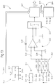
- FIG. 1 of the appended drawings in which an analog / digital converter 201 of the first order sigma-delta type 201 has been schematically represented, this converter comprising an integrator 202, a comparator 203, a single-bit digital / analog converter 204, a low-pass digital filter 205 and a signal combining circuit 6.
- the A / D converter 201 also includes an input terminal 207, an output terminal 208 and a data terminal 209.
- An analog input signal is applied to the input terminal 207 and transmitted to the integrator 202 via the combination circuit 206.
- the comparator 203 samples the signal from the integrator 202 at a sampling frequency f s which is N times higher than the Nyquist frequency f N (f N is twice the highest frequency of the signal). N is called "oversampling factor".
- f s the sampling frequency
- f N the Nyquist frequency
- N is called "oversampling factor”.
- rough estimates (at 1 bit) of the analog input signal appear at the output of comparator 3 at the rate of the oversampling rate. These estimates are in the form of a bit stream at data terminal 209 and they are converted to analog form by the D / A converter 204, while being subtracted from the analog input signal by the combination circuit. signals 206.
- the bit stream coming from the output of comparator 203 contains information composed of the analog input value, in digital form, as well as a digital error signal which is also called "quantization error” or "quantization noise
- the quantization error or noise r (t) represents the error between the linear model and the initially non-linear transfer.
- Y (s) I (s) + 1 / (1 + cG (s)) .R (s) Consequently, I (s) is not deformed and the quantization noise R (s) is transferred by a high-pass filter 1 / (1 + cG (s) ), which achieves maximum attenuation of the error of quantization for frequencies of the baseband and also an attenuation which decreases progressively for the frequencies which are beyond of the baseband. This process is called "noise shaping". The higher frequency errors which are contained in the bit stream are suppressed by the low pass digital filter 205.
- the dynamic range of the sigma-delta converter 201 can be improved by using instead of the integrator 202 represented in FIG. 1, either a second order or higher order integrator, or a second order or higher order low pass filter, or again a series of two or more two integrators or filters of this type.
- a multi-range signal converter has at least two input ranges, each of which is defined by a maximum value of the input signal, which the converter can accept.
- a diagrammatic representation of such a converter is shown in FIG. 2 of the appended drawings in the form of an analog / digital converter 210 comprising a conventional circuit 211 A / D converter, circuits 212 and 213 for combining signals and an inverter circuit 214.
- An analog signal V in is amplified by a gain G in the circuit 212 of signal combination.
- the amplified signal G * V in is converted into a digital output signal B by the circuit A / D 211.
- the output signal B is then amplified by the inverse of the gain G in the signal combination circuit 213.
- a digital signal B / G representing the analog input signal V in .
- the different ranges of the converter 210 correspond to different values of the gain G that can be chosen, each range having the same number of quantization steps, a number which is determined by the conversion algorithm of the A / D circuit 211.
- C ' this is why the magnitude of the quantization step in the different ranges is directly proportional to the maximum value of the input signal. Therefore, the beaches at low resolution allow the conversion of signals, having high amplitudes, with a relatively large quantization step, while the high resolution ranges allow the conversion of signals of lower amplitude but with a relatively smaller quantization step.
- indirect or interpolation converters have a relative precision which, because of the interpolation which they operate with respect to time, is not limited by the adaptation tolerances of the components. Therefore, sigma-delta converters with 16-bit resolution are often used in applications where resolution and relative accuracy are important factors.
- sigma-delta converters are circuits that have memory. This is why sigma-delta converters are not often used in applications where a signal converter with multiple input ranges is required. More precisely, if in a sigma-delta converter, the range of the input signal is modified, transients are found, that is to say additional noise in the output signal. This noise, which is called “switching noise", comes from the fact that when the integration function is performed, the integrator 202 of the sigma-delta converter 201 accumulates the quantization error between the signal input and output signal. So if we used a sigma-delta converter in a conventional multi-range converter, the accumulated quantization error would be multiplied by the gain G of the range used at a given time. If then the range of the converter, that is to say the value of G, was changed, the function of the integrator would change, but the charge of its capacity would remain the same.
- the charge accumulated in the integrator just before time t1 would represent G1 ( ⁇ t1 e (t) .dt), in which and represents the quantization error.
- the charge accumulated in the integrator would represent G2 ( ⁇ t1 e (t) .dt).
- the fact that the charge of the integrator does not vary at time t1 alters the relationship with the integration process; which results in the appearance of switching noise or in other words transients in the bit stream produced by the integrator.
- An object of the present invention is therefore to provide a circuit, the transfer characteristic of which depends on state variables, which is capable of operating in association with a variable gain circuit without its signal being disturbed by transients as a result. of each change of said variable gain.
- the present invention achieves this object by providing a processing circuit for producing a variable output signal in response to a variable quantity sensed or received at the input, said processing circuit being associated with a stage or with an input sensor supplying a signal. with a variable amplification / attenuation factor and said processing circuit further having response characteristics which depend in particular on state variables, characterized in that it comprises means for suppressing the transients normally produced by a modification of said factor amplification / attenuation, said transient suppression means operating by modifying the value of said state variables in direct proportion to said modification of the amplification / attenuation factor.
- the amplification / attenuation factor can be varied without causing transients.
- this variable amplification / attenuation factor it is possible to produce circuits whose operating regime is always close to the optimum both in terms of signal / noise ratio and energy consumption . And this, whatever the intensity of the quantity captured or received as input.
- the invention provides a processing circuit constituting a sigma-delta converter intended to convert a variable input signal into a variable output signal, this converter comprising a signal combining circuit intended for adding the output signal and the input signal or subtracting the output signal from the input signal so as to produce a combined signal, an integrator for integrating the combined signal so as to produce an integrated signal, the integrator comprising an error storage circuit for storing a quantity representing the time value of said combined signal, a comparator for comparing said integrated signal with at least a predetermined level so as to produce said output signal, a feedback circuit intended to apply to said combination circuit a feedback signal representing said sig output signal, a circuit for amplifying said input signal with a predetermined amplification / attenuation factor, a range adjustment circuit intended to change said amplification / attenuation factor from a first value to at at least a second value, a circuit for amplifying said output signal by the inverse of said amplification / attenuation
- the invention also relates to a processing circuit constituting a sigma-delta converter intended to convert a variable input signal into a variable output signal, this converter comprising a signal combining circuit intended to generate a combined signal resulting from the adding a feedback signal representing said output signal and said input signal, or subtracting this feedback signal from said input signal, an integrator for integrating said combined signal so as to generating an integrated signal, said integrator comprising an error storage circuit for storing an amount which represents the time value of said combined signal, a comparator for comparing the integrated signal with at least a predetermined level so as to generate said output signal , a feedback circuit for providing a feedback signal which represents said if general output to said signal combination circuit, a circuit for amplifying the output signal by the amplification / attenuation factor so as to generate said feedback signal, and a range setting circuit for changing said boost / cut factor from a first value to at least a second value.
- a processing circuit constituting a sigma-delta converter intended to convert a variable
- the quantization error accumulated in the integrator is independent of the amplification / attenuation factor of the particular range which has been chosen, the introduction of switching noise into the output signal of the sigma-delta converter is avoided.
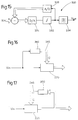
- FIG. 3 is the block diagram of an analog circuit according to the present invention.
- FIG. 3 essentially comprises four blocks which respectively symbolize a circuit for processing a signal 2, a first amplification / attenuation stage with variable gain 4, a block 6 grouping together gain control means and means for suppressing transients and, finally, a second amplification / attenuation stage with variable gain 8 to restore the signal to its original level.
- block 8 may be implicit. In the case of a multi-meter, for example, it is the operator who determines the measurement scale to be considered by knowing the position of the range selector.
- the general operating principle is as follows.
- the signal to be processed is firstly supplied by a line 10 at the input of the first amplification / attenuation stage 4 which, in response to this signal, outputs at a line 12 a signal whose amplitude is normalized .
- the amplification / attenuation stage 4 is provided to be controlled by the gain control means.
- the different values that the gain can take are denoted K0, K1, ..., K n .
- the gain can take either a set of discrete values (this is called a switchable gain), or vary continuously within a certain interval.
- the signal amplified by the amplification / attenuation stage is supplied, via line 12, to the input of the signal processing circuit 2.
- the circuit 2 In response to this signal on its input, the circuit 2 outputs a processed signal on a line 14.
- Signal processing can be of all known types (filtering, analysis, analog / digital conversion, etc.).
- a line 16 extending between a node 15 on the line 14 and the block 6.
- This line 16 is used to apply the level of the signal supplied at the output of the processing circuit 2 to the gain control means of block 6, so as to allow the latter to determine when the gain of stage 4 must be changed.
- Those skilled in the art will understand that instead of checking the level of the signal at the output of the processing circuit 2, it would also be possible to measure the level of the signal at the input, of the signal at the output of the first stage 4 or at any other place. of the diagram in Figure 3.
- the operating principle of the gain control means 6 is as follows; if at some point the signal level on line 16 exceeds a certain fraction, for example 90%, of the total dynamics of circuit 2 or if, on the contrary, this level falls below a certain fraction, for example 25 %, of the dynamics, the gain control means react by controlling the two amplification / attenuation stages 4 and 8 so as to change their gain, so as to reduce the level of the signal at the input of the processing circuit 2 to a value as close as possible to the maximum admissible by the latter.
- a certain fraction for example 90%
- the gain control means react by controlling the two amplification / attenuation stages 4 and 8 so as to change their gain, so as to reduce the level of the signal at the input of the processing circuit 2 to a value as close as possible to the maximum admissible by the latter.
- the two lines 18 and 20 are intended to supply each of the stages 4 and 8 a control signal in response to which each of stages 4 and 8 will change gain.
- the gain control means and the amplification / attenuation stages are provided to cooperate so that, when the gain of the first stage 4 changes in a given ratio, the gain of the second stage 8 changes in an inverse ratio to that from the first floor.
- Such an arrangement is important when for example the signal to be processed is an audio signal which one wishes to filter.
- the second amplification / attenuation stage 8 may not be explicitly present as in the measurement instruments already mentioned.
- the module 6 of FIG. 3 still comprises, according to the present invention, a sequencer which is associated with the gain control means, and which ensures, via line 22, the control of the suppression means transients according to the present invention.
- the means for suppressing transients are provided so as to modify the values of the state variables of the processing circuit 2 each time the gain of the amplification / attenuation stage 4 changes. Furthermore. the modification of the state variables is made in proportion to the variation of the gain of the first stage 4. Experience shows, in fact, that such a modification of the state variables makes it possible to almost completely remove the transients and the components undesirable in the output of the processing circuit 2.
- the circuit shown diagrammatically in FIG. 4 constitutes a first particular example of a circuit for processing a signal which is generally represented in FIG. 3 by the block referenced 2.
- the diagram in FIG. 4 represents a continuous second order pass filter -band / low pass using operational amplifiers with transconductance and capacities (OTA-C). This type of filter is known to those skilled in the art. Indeed, it is widely used in analog integrated embodiments, for signal processing.
- OTA-C operational amplifiers with transconductance and capacities
- the circuit of FIG. 4 comprises an input line 12 for receiving a signal to be filtered supplied by the first amplification / attenuation stage (FIG. 3) and two output lines 14a and 14b intended to be used alternatively to provide either a low pass filtered signal or a band pass filtered signal.
- the circuit 2 comprises two capacitors, of capacitance C1 and C2 respectively, referenced 24a and 24b. These capacitors 24a and 24b are each connected between a node of the circuit (referenced 26a and 26b respectively) and the ground. As seen in the figure, the nodes 26a and 26b are each located downstream of an amplifier (referenced 28a and 28b respectively). It will be understood from the preamble to the description that, in the circuit shown here, it is the capacitors 26a and 26b which store the memory of the circuit. Consequently, in the present example, the state variables which must, in accordance with the present invention, be modified by the means for suppressing the transients are the respective charges of the two abovementioned capacitors.
- FIG. 5 represents one of the capacitors 24a or 24b of FIG. 4 with the means for suppressing the transients which, according to the present invention, are associated with it.
- the capacitor 24 of capacity C represents one of the capacitors 24a or 24b
- the node 26 represents one of the nodes 26a or 26b
- the transconductance amplifier 28 represents one of the transconductance amplifiers 28a or 28b.
- FIG. 5 The other elements shown in FIG. 5 are part of the means for suppressing transients according to the present invention.
- the particular means of suppressing the transients described in this first example are provided for a situation where the amplitude of the signal at the input of the circuit of FIG. 4 has previously been normalized by an amplification / attenuation stage, the gain of which can take different discrete values having between them relationships which are powers of 2.
- these means comprise a capacitor 30, having the same capacitance C as the capacitor 24, an operational amplifier 32 and seven switches referenced, respectively, ⁇ 1, ⁇ 1b, ⁇ 1c, S1, S2, S3 and S4.
- the circuit described in FIG. 5 is a circuit of the switched capacity type.
- the switches can be controlled by control signals conventionally generated by a sequencer (already mentioned in connection with FIG. 3) itself responding to the control signals produced by the gain control means (referenced 6 in FIG. 3 ).
- the control signals, generated by the sequencer are supplied to the various switches by transmission lines which are not shown.
- the means for suppressing the transients are therefore provided for modifying the values of the state variables by any power of 2.
- the sequencer controlling the transient suppression means, becomes operational. It first generates a first command signal to open the switches ⁇ 1 and ⁇ 1b and to close the switch ⁇ 1c and the switches S1 and S2. The first result of these switches is to isolate the first capacitor 24 and its contents from the rest of the circuit. In addition, closing the switch ⁇ 1c has the effect of connecting the capacitor 24 between the output and the virtual ground of the amplifier 32 so that its charge is, initially, kept constant. Finally, the closing of the switches S1 and S2 has the effect of completely discharging the second capacitor 30.
- the sequencer sends a second control signal to open the switches ⁇ 1c, S1 and S2 and close the switches S3 and S4 so as to connect the two capacitors 24 and 30 in parallel. Under these conditions, half of the charge present in the capacitor 24 passes through the capacitor 30 to equalize the voltages between the terminals of the two capacitors. This charge transfer has the effect of dividing by 2 the value of the state variable stored in the capacitor 24.
- the sequencer finally sends a third control signal to return the switches to their initial configuration (all switches open except ⁇ 1 and ⁇ 1b).
- the sequencer controlling the transient suppression means becomes operational. It first generates a first control signal identical to the first control signal of the divide by 2 sequence described above.
- This control signal has the effect open the switches ⁇ 1 and ⁇ 1b and close the switch ⁇ 1c.
- the first result of this switching is to isolate the capacitor 24 and its content from the rest of the circuit.
- closing the switch ⁇ 1c has the effect of connecting the capacitor 24 between the output and the virtual ground of the amplifier 32 so that its charge is, initially, kept constant.
- the sequencer sends a second control signal to close the switches S2 and S3.
- the operational amplifier 32 charges the capacitor 30 until the voltage between its terminals is equal to the voltage between the terminals of the capacitor 24.
- the capacity of the capacitor 30 being identical to that of the capacitor 24, it will contain the same charge as the latter.
- the sequencer then sends a third control signal to open the switches S2 and S3 and close the switches S1 and S4. Under these conditions, the charges contained in the capacitor 30 cause a modification of the potential at the inverting input of the amplifier 32 which, in response, provides charges to the capacitor 24 until the potential of its inverting input again that of mass. This last operation results in a doubling of the voltage between the terminals of the capacitor 24.
- the sequencer finally sends a fourth control signal to return the switches to their initial configuration (all the switches open except ⁇ 1 and ⁇ 1b).
- a switching sequence like that which has just been stated can be carried out in a much shorter time than the duration of the transient disturbances which are observed in the absence of the means for suppressing the transients according to the invention.
- the cut produced in the signal by the transient suppression means may even be imperceptible.
- the change of the state variables can be carried out within one or more periods of the carrier.
- FIG. 6 therefore represents a second embodiment of the means for suppressing transients according to the present invention.
- the means for suppressing the transients are used to change the value of the state variable associated with the capacitor 24b with capacitance C2 in FIG. 4.
- the components shown in FIG. 6 which are already shown in FIG. 4 have the same reference numbers.
- the circuit of FIG. 6 operates by virtue of a block 35 supplying a current at output, the intensity of which is equal to the product of the intensity of the input current by the amplitude of a control signal.
- This block 35 is adapted to, on the one hand, supply on its output 60 a current KI which is equal to K times the current I received on its input 50 and, on the other hand, to ensure that the input 50 remains at the mass.
- This block 35 can be produced in the manner presented to ISCAS 1989 by Adel S. Sedra under the title "the current conveyor; history and progress", and by using a current mirror with variable ratio.
- These means for removing transients comprise two identical capacitors, a first of the two (for example the capacitor 24) fulfilling at a given moment the function of the capacitor 24b in the circuit of FIG. 4.
- the first capacitor is discharged through block 35.
- Block 35 then supplies, at output, a current whose intensity is equal to the intensity of the current produced by the discharge of the first capacitor multiplied by a factor K given.
- the current at the output of block 35 is used to charge the second capacitor which, at the end of the operation, has between its terminals a voltage equal to the voltage which previously existed between the terminals of the first capacitor multiplied by said given factor.
- the circuit of FIG. 6 includes a switch 1 which corresponds to the switch 1 of FIG. 5 and a series of pairs of switches S1a, S1b, S2a, s2b, S3a, S3b, S4a, S4b, S6a, S6b, S7a and S7b.
- the capacitor 24 is associated with the switches Sa while the capacitor 24 'is associated with the switches Sb.
- a resistor 37 is finally mounted at the input of the multiplier 35 to slow the discharge of the capacitor when the value of the state variable changes.
- the switch 1 In the absence of a gain change in the amplification / attenuation stage, the switch 1 is closed. We will assume here that before the gain change, the capacitor 24 was connected to the filter. Under these conditions, the switch S1a is closed and the switch S1b is open. In addition, the switches S3a, S4a, S6a and S7a are also open while the switch S2a is closed. Note also that the switches S2b and S7b are closed to keep the capacitor 24 'fully discharged and that the switches S3b, S4b and S6b are open.
- the sequencer controlling the transient suppression means becomes operational. It generates, on the one hand, a first control signal to open the switch 1 and decouple the capacitor 24 from the rest of the circuit and on the other hand it transmits to block 35 a signal corresponding to the given factor by which the gain at input of the filter will be multiplied.
- the switches S4a, S7a, S2b and S6b are closed while the switch S2a is open.
- the capacitor 24 will discharge through the resistor 37 in the input of the block 35.
- all the current supplied at the output of the multiplier 35 will accumulate in the capacitor 24 '.
- the charge which will accumulate in the capacitor 24 ′ will be proportional to the charge initially contained by capacitor 24.
- the multiplication factor K of block 35 being determined by the factor by which the gain control means modifies the gain, the ratio between the charge of the capacitor 24 'and that of the capacitor 24 will be equal to the factor by which the gain is changed.
- the sequencer sends a control signal to close the switch S1b and close the switch 1 so as to couple the capacitor 24 'with the circuit.
- FIG. 7 shows another example of application of the present invention.
- the device shown diagrammatically in FIG. 7 is designed to provide a variable signal at the output in response to a variable quantity picked up at the input by a sensor which in the present example is of the capacitive type.
- the device firstly comprises a capacitive sensor with two capacitors 110.
- the output of the sensor 110 is connected to the input of a processing and interface circuit 120 which can typically be constituted by a Sigma-Delta bandpass modulator.
- the Sigma-Delta 120 modulator provides a bit train modulated in pulse density.
- This bit stream is supplied to a synchronous digital detection module 130 controlled by a time base signal supplied on a line 180 by a clock. 160.
- the module 130 supplies in response a digital signal which constitutes the output signal of the device.
- the bit stream produced by the processing circuit 120 is also supplied to a module 140 which essentially functions as a low-pass filter to produce an analog output signal from the pulse density modulated signal.
- the analog signal produced by the module 140 is still transmitted by a line 170 to the sensor 110 so as to constitute a feedback loop to, for example, maintain the sensor in a state of equilibrium .
- the capacitive sensor 110 may, in known manner, be of the type comprising two capacitors and in which a movable conductive strip constitutes a common movable frame for the two capacitors. With such an arrangement, any movement of the movable blade results in a variation of the respective capacities of the two capacitors. This variation in the capacitances of the two capacitors is typically measured by respectively placing the fixed plates of the two capacitors with two imposed potentials of the same value but with opposite signs, and by measuring either the charge or the potential on the moving blade. It should be noted that with such an arrangement the intensity of the measurement signal, or in other words the sensitivity of the sensor, is proportional to the modulus of the potential imposed on the fixed armatures.
- the devices corresponding to the part of the functional diagram of Figure 7 which has been described so far can be made with known elements.
- a particular example of such a device is the device for measuring a force described in document EP 0 590 658.
- a modulator such as that described in the article entitled "A Fourth -Order Bandpass Sigma-Delta Modulator "by Stephen A. Jantzi et al. and appeared in the IEEE Journal of Solid-State Circuits, Vol. 28, No. 3, March 1993.
- the device of FIG. 7 also comprises a module 150 which fulfills the same functions as the means represented by block 6 in FIG. 3.
- the module or block 150 controls the level at the output of the treatment circuit 120 at l using line 154 so as to determine when the sensitivity of sensor 110 should be changed.
- FIG. 7 also shows a control line 156 which allows the block 150 to control a block 100 which is provided to supply the two reference potentials for the fixed armatures of the capacitive sensor 110.
- the processing circuit 120 includes a memory
- the variations caused by the sensitivity of the sensor will, as in the case of the device in FIG. 3, cause the appearance of transients.
- the device of FIG. 7 comprises means for suppressing the transients (symbolized by the line 190) which can be produced in a completely analogous manner to those which have been described with reference to FIG. 5 or to Figure 6.
- FIG. 8 it can be seen that it represents a sigma-delta converter 220 at multiple ranges comprising a signal combination circuit 221, an integrator 222, a comparator 223, a feedback circuit 224, an amplifier 225 of the input signal, a range adjustment circuit 226, an amplifier 227 of the signal output Y and a noise compensation circuit 228.
- the input signal amplifier 225 comprises four capacitors 229, 230, 231 and 232. One of the plates of capacitors 229, 230, 231 and 232 is connected respectively to one of the terminals of the switches 233, 234, 235 and 236.
- the integrator 222 comprises an operational amplifier 237, a capacitor 238 of which is connected between its inverting input and its output.
- the integrator 222 generates, at its output, an analog voltage which represents the integration with respect to time of the total charge stored by the capacitors 229 to 232 and 257.
- the other terminals of the switches 233, 234, 235 and 236 are connected set at the inverting input of the operational amplifier 237 via a switch 239.
- Two terminals 240 and 241 are connected to the input signal amplifier 225 via two switches 242 and 243 of so that an analog voltage V in present at these terminals can be applied to one or more of the capacitors 229, 230, 231 and 232.
- the capacitors 229, 230, 231 and 232 have the same value C in .
- the range setting circuit 226 includes a switch control circuit 244 and the switches 233, 234, 235 and 236.
- a data bus 245 transmits a signal which represents the desired gain G of the input signal of the sigma converter. delta 220, to circuit 244 for controlling switches.
- This circuit has four outputs 244a, 244b, 244c and 244d to respectively control the operation of switches 233, 234, 235 and 236.
- the operation of switches 233, 234, 235 and 236 is controlled respectively as a function of the gain signal received from the bus 245, so that the input voltage V in present between the terminals 240 and 241 can be applied to one of the capacitors 229, 230, 231 and 232 or to a combination of these capacitors connected in parallel.
- the noise compensation circuit 228 comprises a circuit 250 for controlling switches and gain detection intended to detect a variation in the value of the gain signal coming from the bus 245 and to control the respective operation of the contactors 246, 247, 248 and 249 via its outputs 250a, 250b, 250c and 250d, so that the capacitors 238 and 245 are connected, either in parallel or in series between the operational amplifier 237 and the ground.
- the comparator 223 compares the voltage level at the output of the operational amplifier 237 with a predetermined reference voltage, which is in the case shown, the ground potential. If the output voltage of the operational amplifier is greater than zero volts, the comparator produces a bit of value +1 at its output, while when this voltage is less than zero volts it produces a bit of value -1. In the data bit stream, carrying the reference Y, which is thus produced by the comparator 223, the density of the bits of high logic level relative to that of the level bits logic low, represents the analog input voltage V in applied between terminals 240 and 241.
- the feedback circuit 224 comprises a bit detector and a circuit 251 for controlling switches, two terminals 252 and 253, switches 239, 254, 255 and 256, a capacitor 257 having a value C ref and a source of voltage V ref (not shown).
- the control circuit 251 has outputs 251a and 251b to allow the control of the switches 254 and 255, respectively.
- the switches 254 and 255 allow the capacitor 257 to be changed with a charge Qref equal to C ref * V ref , or to discharge this capacitor.
- the load Q ref is integrated in the positive direction or in the negative direction. The difference between the charges Q in ⁇ Q ref is thus stored between the armatures of the capacitor 238 and correspondingly integrated by the operational amplifier 237.
- the stability of the sigma-delta converter 220 is guaranteed as long as the charge Q in associated with the input signal is less than the absolute value of the charge Q ref injected by feedback.
- the input signal V in can thus be sampled with a gain of 1, 2, 3 or 4 in controlling switches 233, 234, 235 and 236 so as to choose the corresponding number of capacitors 229, 230, 231 or 232.
- the multiplication of the input signal by a desired gain can be achieved in another way, for example by a programmable current mirror or by other circuits in which the active elements are different from capacitors 229, 230, 231 and 232.
- the gain chosen can be greater or less than 1 and take values other than positive integers (1, 2, 3 and 4) of FIG. 8.
- positive integers as gain values simplifies the operation of the division performed by logic circuit 227.
- the values of the chosen gain correspond to powers of two (that is to say the gain can take values such as 4, 2, 1, 1 / 2, 1 / 4, ...) so that the division of the digital word produced by the logic circuit 227 implies a simple shift of the bits in the word.
- the voltage V amp should be equal to ⁇ t1 2 (Vin * Cin - X * Vref * Cref).
- the charge stored by the capacitor 238 remains at this instant always equal to ⁇ t1 (V in * C in - X * V ref * C ref ), so that there is no longer a correct relationship between the function of the integrator and the charge on its capacitor.
- the circuit 250 for controlling the switches momentarily closes the switches 247 and 248 which charges the capacitor 245 has the same value as the capacitor 238. Then the switches 247 and 248 are open, then the switches 246 and 249 are closed. Thus, the capacitor 245 is discharged and its charge is transferred to the armatures of the capacitor 238.
- the switch control circuit 250 first discharges the capacitor 245 by temporarily closing the switches 248 and 249. Then the switches 246 and 247 are closed, which connects the capacitor 245 in parallel with the capacitor 238. If a value equal to that of the capacitor 238 is chosen for the capacitor 245, the charge stored between the plates of the capacitor 238 is reduced by half. The capacitor 245 is then disconnected from the integrator 222. The charge stored by the integrator 222 then becomes ⁇ t1 (V in * C in - X * V ref * C ref ) and the error which is accumulated there is reduced by half to compensate for the halving of the chosen gain.
- the sigma-delta converter in Figure 8 is a particular example of how the switching noise that results from a change in the range of the input signal can be compensated for by multiplying the error accumulated in l 'integrator by a ratio R of the newly chosen gain compared to the previously chosen gain.
- This operation can be implemented more easily if the relation R between the various successive gains is constant, because in this case, it suffices to carry out a multiplication and a division of the error accumulated by the relation R.
- the value of R can conveniently be equal to 2.
- the use of capacitors 238 and 245 in Figure 8 is a practical example of such an embodiment.
- the sigma-delta converter described with reference to FIG. 8 converts an analog input voltage into a digital output word, but it is clear that, according to the present invention, the use of this converter is not limited to this application.
- the invention can be applied in the case where a capacitance is measured which is converted into a variable output signal.
- the capacitors 229, 230, 231 and 232 can be replaced by a voltage source having four predetermined values which are applied across the capacitors to be measured according to a chosen gain of the input signal.
- the input signal applied to the sigma-delta converter of the present invention may be an analog current directly sent to the integrator 222, in which case the input signal amplifier comprises an adjustable current amplifier or a network of resistors.
- the input signal amplifier comprises an adjustable current amplifier or a network of resistors.
- FIG. 9 shows an oversampling digital / analog converter 270 comprising a multi-range sigma-delta converter 271 intended to convert a digital quantity at n bits into a digital quantity at m bits.
- the converter 270 includes a digital interpolation filter 272, an elementary digital / analog converter 273 and an analog low-pass filter 274.
- An input signal X is constituted by an n-bit digital word which is applied to the interpolation filter 272.
- the signal X is first interpolated and then sampled at a frequency f s in the filter interpolation 272, f s being significantly greater than the Nyquist frequency f N of the input signal X.
- the sigma-delta converter 271 is used as a digital noise conformator, operating at a frequency d 'clock f s , which "approximates" the signal X1 of the interpolation filter so as to obtain a signal X2 which consists of a digital word with m bits, n> m.
- the noise generated by the approximation is thus rejected towards frequencies higher than the sampling frequency f s .
- the word "approximate" X2 is converted into an analog signal V1 by the elementary digital / analog converter 273 before passing through the low-pass filter 274 which eliminates the approximation noise rejected towards the higher frequencies.
- the oversampling digital / analog converter 270 also includes a bus 275 intended to apply the chosen gain G to the sigma-delta converter 271 and to the elementary D / A converter 273.
- the signal X1 is multiplied by the gain G so that the signal X2 is better suited to the input range of the elementary D / A converter 273.
- the signal X2 has been converted to analog form, it is divided by G so that the filtered output signal V out represents the digital input signal X.
- a sigma-delta converter (digital noise shaper) 280 has been represented comprising an integrator 281, a truncator 282 and a subtraction circuit 283.
- the integrator 281 comprises a digital register 284 and an addition circuit 285.
- a digital signal X in with n bits is applied to the converter 280.
- a digital signal Y out with m bits which will be described briefly below, n> m, is subtracted from the signal X in and the resulting signal X diff at n bits is applied to the integrator 281.
- the integration is carried out according to an algorithm which adds the output of the register 284 generated during a cycle of previous clock at signal X diff and temporarily stores the resulting sum in the register during the current clock cycle.
- the n bit signal X in from the integrator 281 is truncated to form an output signal Y out comprising the m most significant bits of the signal X int .
- the signal Y out also provides a feedback signal which is subtracted from the input signal X in by the subtraction circuit 283.
- a comparison of the sigma-delta converter of FIG. 1 with the digital noise shaper of FIG. 10 shows that the analog input signal is replaced by a n-bit digital signal, that the integrator 202 is replaced by the integrator 281 purely digital and the comparator 203 is replaced by the truncator 282.
- the output of the D / A converter 204 is replaced by the signal Y out which does not need a physical circuit to be generated due to the division of the bus X int in two parts by the truncator 282.
- the circuit 206 for combining signals is replaced by the subtraction circuit 283.
- the digital noise shaper 280 of Figure 10 is a functional equivalent of the sigma-delta converter 201 of Figure 1.
- the digital noise shaper 280 interpolates and oversamples the signal X in at n bits of so as to produce an output signal Y out which provides an estimate at m bits of the input signal X in .
- the quantization error resulting from the sampling process is rejected towards the higher frequencies by the integrator which is used to carry out the sigma-delta conversion.
- FIG. 10 shows a digital noise shaper 290 in which this simplification has been implemented.
- the digital noise shaper 290 includes the digital register 284, the truncator 282 and the addition circuit 285 of FIG. 10, however that in this embodiment of the invention, the most significant bits Y lsb are accumulated up to that they produce an overshoot of the Y msb signal and are thus transferred to the output of the Y out clipper.
- the converter 290 thus stores the conversion error between its input signal and its output signal.
- a variation in the gain of the input signal alters the relationship between the function of the integrator and the digital value stored in the accumulator, which can be avoided by multiplying the conversion error by the ratio of new gain to old gain.
- FIG. 12 shows an embodiment of the sigma-delta converter 271 with multiple ranges of FIG. 9.
- the latter comprises the converter 290 of FIG. 11 and two multiplication circuits 291 and 292.
- the multiplication circuit 291 multiplies the signal d input X in by the gain signal G (k) chosen from the bus 275.
- the value of the gain G (k) can be changed according to the choice of the range of the input signal from the converter 271.
- the error between the input signal X in and the output signal Y out is accumulated in the digital accumulator 284 with a gain which depends on the chosen range, the change in the range of the input signal introduces switching noise into the stored conversion error.
- the multiplication circuit 292 is connected in the feedback circuit between the truncator 282 and the addition circuit 285, in order to multiply the signal Y lsb by the ratio of the new gain G (k) to the old gain G (k-1).
- the position of the bits in each of the digital words X in and Y lsb can be offset by an appropriate number of locations. This can preferably be done using shift registers, the gain signals G (k) and G (k) / G (k-1) determining the number of positions by which the bits are to be shifted.
- FIG. 13 shows in general a sigma-delta A / D converter 100 comprising the integrator 222, the comparator 223 and an amplifier 227 of the output signal of the sigma-delta converter 220.
- the sigma-delta converter 300 comprises a signal combining circuit 301, an amplifier 302 of the signal of feedback, a range setting circuit 303 and a feedback circuit 304.
- the feedback amplifier 302 comprises four capacitors 305, 306, 307 and 308.
- the armatures of these capacitors are respectively connected to the switch terminals 309, 310, 311 and 312.
- the other terminals of these switches are connected together to the non-inverting input of an operational amplifier 237 via switch 256.
- the voltage V ref present at terminals 252 and 253 is applied to one or more of the capacitors 305, 306, 307 and 308.
- these capacitors Preferably, these capacitors have the same value C ref .
- the range adjustment circuit 303 comprises a circuit for controlling switches 313 as well as switches 309, 310, 311 and 312.
- the circuit 313 has four outputs 313a, 313b, 313c and 313d for controlling the operation of the switches 309 respectively. 310, 311 and 312.
- the operation of the switches is selectively controlled as a function of the gain signal from the bus 245 so that any combination of the capacitors 305, 306, 307 and 308 can be connected so as to receive the voltage V ref .
- the charge stored between the armatures of the capacitors connected in parallel can thus be equal to C ref * V ref , 2C ref * V ref , 3C ref * V ref or 4C ref * V ref , depending on the gain that is present on the bus. 245.
- the input signal V in present between terminals 240 and 241 is applied to the terminals of a capacitor 314 whose value is C in , by means of switches 242 and 243.
- a charge Q in equal to V in * C in is thus produced between the armatures of the capacitor C in .
- This load is applied to the inverting input of the operational amplifier 237 via the switch 239.
- the feedback circuit 304 includes a control circuit 315, terminals 252 and 253, the contactors 239, 254, 255 and 256 and the voltage source V ref .
- the control circuit 315 detects the digital word at the output of the amplifier 227 of the output signal, this word resulting from the multiplication of the digital information in the bit stream coming from the comparator 223 by the inverse of the gain on the bus 245.
- the control circuit 315 has outputs 315a and 315b to allow control of the operation of the switches 254 and 255, respectively.
- the load G * Q ref is integrated either positively or negatively depending on the value +1 or -1 of the bit produced at the output of comparator 223, by controlling the operation of switches 254 and 255.
- the difference between the charges Q in ⁇ G * Q ref is stored between the armatures of the capacitor 238 and is thus integrated by the operational amplifier 237.
- the sigma-delta converter 300 is stable as long as the charge Q in is less than the absolute value of the reaction charge Q ref .
- the range of the input signal for the input signal V in can thus be chosen according to the number N of capacitors 305, 306, 307 and 308 connected in parallel.
- the capacitor 238 of the integrator 222 accumulates the difference between the analog input signal and the digital output signal reconverted into analog form.
- the switching noise is introduced at the moment when the range of the input signal is modified due to the alteration of the relation between the gain of the input signal V in and the quantization error stored by the capacitor 238. This noise is avoided by multiplying the quantization error by the ratio of the new gain to the old gain.
- the integrator 222 accumulates the quantization error independently of the gain chosen.
- the output V amp of the operational amplifier 222 is equal to A ( ⁇ t1 e (t) .dt), where A represents the fixed gain of the input signal V in . Any alteration of the relationship between the gain of the input signal and the error accumulated in the integrator of the sigma-delta converter and consequently any switching noise which could result therefrom is thus avoided.
- the sigma-delta converter 300 of FIG. 13 can also be produced in the form of a digital noise shaper intended to convert a digital signal of n bits into a digital signal of m bits.
- FIG. 14 shows, in general, such a sigma-delta converter 320 comprising the digital accumulator 284 and the addition circuit 285 of FIG. 12 and, moreover, a programmable truncator 321.
- the number of bits in the signal Y lsb and consequently of the complementary signal Y msb is modified by the truncator 321 in response to the value of the selected gain G which is applied to it; which allows the converter 321 reaction circuit to be programmed.
- the sensitivity of the converter 321 can be increased by reducing the number of the least significant bits accumulated and consequently by producing a faster exceeding these bits in the most significant bit of signal X1.
- the accumulator always accumulates the difference between the input signal X in and the output signal Y out regardless of the range chosen for the converter 320, the digital value stored in the accumulator 284 need not be update, when the chosen range is modified.
- the sigma-delta converter in FIG. 14 has the advantage of greater simplicity compared to the sigma-delta converter 271 represented in FIG. 12.
- FIG. 15 represents, in general, a digital / analog converter 330 with oversampling mounted in closed loop.
- the converter 330 has a direct circuit with a basic D / A converter 331 and an integrator 332, as well as a feedback circuit which includes an analog / digital converter 333.
- a low-low filter 334 eliminates high frequency noise of the voltage at the output of the integrator 332.
- the accuracy of the sigma-delta converter 330 is essentially determined by the feedback circuit.
- the sigma-delta converter 330 can thus be produced by using a precise A / D converter 333 and a more basic D / A converter 331.
- the sigma-delta converter of the The present invention in the form described for example in connection with FIGS. 8 and 13, is thus ideally suited for use as an A / D converter 333. It is preferable, to confer on the sigma-delta converter of the present invention the best signal-to-noise ratio, optimizing the chosen gain. If the gain chosen is too high, the converter will saturate when either the input signal or the feedback signal exceeds a certain amplitude. This results in "truncation" of the signal and distortion of the output signal. On the other hand, if the gain chosen is too low, the operation of the converter leads to a low resolution and the signal-to-noise ratio is reduced.
- FIG. 16 schematically represents the sigma-delta converter 220 of FIG. 8 and a gain control circuit 340, the latter being able to be used also in the other embodiments of the invention.
- This circuit 340 measures the amplitude of the signal V in but can also measure its energy. Depending of this measured amplitude, the control circuit 340 increases or decreases the value of the gain G on the bus 245 so that it can be used by the sigma-delta converter 220 for adjusting the range of the input signal.
- the control circuit 340 will not be described in detail, because it can be easily carried out by specialists; it can for example comprise a mixed analog / digital circuit comprising threshold detectors, comparators, Schmitt "triggers", low pass filters and / or low resolution A / D converters by means of which this circuit checks the level of the input signal and consequently adjusts the sensitivity of the converter 220 by sending a signal representing the range chosen to the range selection circuit of the converter 220.
- FIG. 17 shows another arrangement in which the sigma-delta converter 220 of FIG. 8 is controlled by a gain control circuit 350 which measures the level of the signal at the output of the converter 220. As the circuit used is then practically only digital, the gain control circuit 220 thus avoids the use of additional analog circuits of the gain control circuit 340 of FIG. 16.
- the scope of the present invention is not limited to circuits comprising a variable gain input stage but that it generally extends to all devices in which the amplitude of a magnitude captured at input can vary predictably and whose variation has an effect comparable to a change in gain.
- the invention remains applicable when the amplitude of the signal undergoes changes, predictable or detectable, comparable to a change in gain due to a disturbance, a change in the characteristics of the processing circuits, etc.
Abstract
Description
La présente invention concerne très généralement les circuits de traitement prévus pour produire un signal de sortie variable en réponse à une grandeur variable captée ou reçue en entrée. La présente invention concerne plus particulièrement les circuits de traitement qui sont associés à un étage ou à un capteur d'entrée fournissant un signal avec un facteur d'amplification/atténuation variable, et elle concerne notamment les circuits pour le traitement de signaux en amont de l'entrée desquels est placé un circuit à gain variable.The present invention very generally relates to the processing circuits provided for producing a variable output signal in response to a variable quantity sensed or received at the input. The present invention relates more particularly to the processing circuits which are associated with a stage or to an input sensor supplying a signal with a variable amplification / attenuation factor, and it relates in particular to the circuits for processing signals upstream of the input of which is placed a variable gain circuit.
Il est classique de prévoir un élément à gain commutable, ou plus généralement à gain variable, en amont d'un circuit pour le traitement d'un signal. Tout le monde connaît notamment l'exemple des volt-mètres à commutation de gamme. D'une manière générale, on a normalement recours à une telle association entre un élément à gain commutable et un circuit pour le traitement d'un signal lorsqu'on désire assurer un rapport signal/bruit constant dans une gamme plus étendue que la gamme dynamique propre du circuit de traitement.It is conventional to provide an element with switchable gain, or more generally with variable gain, upstream of a circuit for processing a signal. Everyone is familiar with the example of range switching volt meters. Generally speaking, such an association is normally used between a switchable gain element and a circuit for processing a signal when it is desired to ensure a constant signal / noise ratio in a wider range than the dynamic range. clean of the treatment circuit.
L'utilisation d'un étage à gain commutable en amont d'un circuit de traitement de signaux peut présenter des inconvénients. En effet, avec de nombreux types de circuits, chaque commutation de gamme de sensibilité entraînent l'apparition de valeurs ou d'états transitoires indésirables (ci-après désignés par transitoires) dans le signal fourni en sortie. Ces transitoires liées à un changement de gamme apparaissent systématiquement dès qu'un circuit donné comprend des composants comme des condensateurs ou des bobines qui, par nature, accumulent des "souvenirs" d'états antérieurs du circuit. Dans ces conditions, on parle de circuits ayant une mémoire, de circuit dépendant de variables d'état ou encore de circuit dont la caractéristique de transfert dépend de variables d'état.The use of a switchable gain stage upstream of a signal processing circuit can have drawbacks. Indeed, with many types of circuits, each switching of the sensitivity range results in the appearance of undesirable transient values or states (hereinafter referred to as transients) in the signal supplied at the output. These transients linked to a change of range appear systematically as soon as a given circuit includes components such as capacitors or coils which, by their nature, accumulate "memories" of previous states of the circuit. Under these conditions, we speak of circuits having a memory, circuit dependent on state variables or circuit whose transfer characteristic depends on state variables.
On comprendra, qu'avec les circuits dont la caractéristique de transfert dépend de variables d'états ou, en d'autres termes, avec les circuits ayant une mémoire, le recours à la commutation de gammes n'est possible que si on donne au circuit le temps de se stabiliser, après chaque changement de gamme, avant d'utiliser le signal qu'il fournit en sortie.It will be understood that with circuits whose transfer characteristic depends on state variables or, in other words, with circuits having a memory, recourse to range switching is only possible if the time to stabilize, after each change of range, before using the signal it provides at output.
Les circuits analogiques ayant une mémoire sont très courants. En effet, Les filtres analogiques les plus courants comportent des composants inductifs ou capacitifs qui gardent la mémoire des états antérieurs, D'autre part, les circuits analogiques les plus précis, comme par exemple les convertisseurs sigma-delta ou les systèmes à verrouillage de phase ou de fréquence (Lock-in), sont basés sur un compromis entre d'une part la précision dans la réalisation de leurs différents composants et d'autre part leur temps de réaction ou leur bande passante.Analog circuits with memory are very common. In fact, the most common analog filters include inductive or capacitive components which keep the memory of previous states. On the other hand, the most precise analog circuits, such as for example sigma-delta converters or phase locked systems. or frequency (Lock-in), are based on a compromise between on the one hand the precision in the realization of their different components and on the other hand their reaction time or their bandwidth.
Dans les amplificateurs "Lock-in", en particulier, on met à profit la périodicité connue d'un signal pour réaliser sa détection dans une largeur de bande extrêmement limitée de façon à le distinguer du bruit ambiant. Dans les modulateurs sigma-delta, par contre, une certaine tolérance quant à la précision de réalisation est compensée par le recours au sur-échantillonage et à une rétro-action quantifiée qui prend en compte les erreurs passées jusqu'à un certain ordre.In "lock-in" amplifiers, in particular, the known periodicity of a signal is used to detect it in an extremely limited bandwidth so as to distinguish it from ambient noise. In the sigma-delta modulators, on the other hand, a certain tolerance as for the precision of realization is compensated by the recourse to oversampling and to a quantified feedback which takes into account past errors up to a certain order.
Afin de permettre une meilleure définition de l'objet de la présente invention, il est utile de mieux caractériser la caractéristique de transfert et les propriétés fonctionnelles des circuits ayant une mémoire.In order to allow a better definition of the object of the present invention, it is useful to better characterize the transfer characteristic and the functional properties of circuits having a memory.
Les caractéristiques fonctionnelles d'un circuit analogique de traitement sans mémoire peuvent être décrites sous la forme d'une combinaison quelconque (éventuellement très complexe) mais fixe de coefficients constants et de quantificateurs. Cette caractéristique de transfert est alors déterminée, et le signal en sortie du circuit à un instant donné est donc déterminé entièrement par la connaissance du signal instantané en entrée.The functional characteristics of an analog processing circuit without memory can be described in the form of any combination (possibly very complex) but fixed with constant coefficients and quantifiers. This transfer characteristic is then determined, and the signal output from the circuit at a given instant is therefore determined entirely by knowledge of the instantaneous input signal.
Dans le cas d'un circuit analogique ayant une mémoire, en revanche, la valeur du signal en sortie ne dépend pas seulement du signal en entrée à un instant particulier, mais également du signal en entrée à d'autres instants antérieurs à cet instant particulier. On peut dire que dans le cas d'un élément de circuit ayant une mémoire, les souvenirs du circuit influencent ses caractéristiques de transfert. En d'autre termes, dans le cas d'un élément de circuit ayant une mémoire, la combinaison de coefficients et quantificateurs qui permet de déterminer la valeur du signal en sortie à partir de la valeur du signal en entrée à un instant donné, est fonction de la valeur du signal en entrée à des instants antérieurs. Un élément de circuit ayant une mémoire sera donc généralement caractérisé, du point de vue fonctionnel, par une combinaison comprenant des coefficients constants et des quantificateurs, mais auxquels s'ajoutent, cette fois, des éléments variables qui gardent la mémoire des instants antérieurs et sont appelés variables d'état. Notons, en particulier, que dans le cas de filtres analogiques, il y aura antant de variables d'état que de pôles.In the case of an analog circuit having a memory, on the other hand, the value of the output signal does not depend only on the input signal at a particular instant, but also on the input signal at other times prior to this particular instant . We can say that in the case of a circuit element having a memory, the memories of the circuit influence its transfer characteristics. In other words, in the case of a circuit element having a memory, the combination of coefficients and quantifiers which makes it possible to determine the value of the output signal from the value of the input signal at a given instant, is function of the value of the input signal at earlier times. A circuit element having a memory will therefore generally be characterized, from the functional point of view, by a combination comprising constant coefficients and quantifiers, but to which are added, this time, variable elements which keep the memory of the previous instants and are called state variables. Note, in particular, that in the case of analog filters, there will be as many state variables as there are poles.
On peut donc dire que la mémoire d'un élément de circuit est stockée dans des variables d'état. Dans un circuit réel, les éléments qui emmagasinent cette mémoire sont les capacités et les inductances. Les variables d'état d'un circuit seront donc défines par des tensions aux bornes de condensateurs, des courants dans des enroulements ou une combinaison des deux. On remarquera, de plus, que toute capacité et toute induction placées sur le chemin du signal constitue une forme d'intégrateur et que, en conséquence, on peut dire que la mémoire d'un élément de circuit est emmagasinée dans des intégrateurs.We can therefore say that the memory of a circuit element is stored in state variables. In a real circuit, the elements which store this memory are the capacities and the inductances. The state variables of a circuit will therefore be defined by voltages across capacitors, currents in windings, or a combination of both. It will also be noted that any capacitance and any induction placed on the signal path constitutes a form of integrator and that, therefore, it can be said that the memory of a circuit element is stored in integrators.
Un exemple particulier d'un circuit ayant une telle mémoire est, comme nous l'avons déjà dit, un convertisseur sigma-delta. Pour permettre d'expliquer les principes de base du fonctionnement d'un convertisseur sigma-delta, on se référera à la figure 1 des dessins annexés sur laquelle on a représenté schématiquement un convertisseur analogique/numérique 201 du type sigma-delta du premier ordre, ce convertisseur comprenant un intégrateur 202, un comparateur 203, un convertisseur numérique/analogique 204 à un seul bit, un filtre numérique passe-bas 205 et un circuit 6 de combinaison de signaux. Le convertisseur A/D 201 comprend également une borne d'entrée 207, une borne de sortie 208 et une borne de données 209.A particular example of a circuit having such a memory is, as we have already said, a sigma-delta converter. To make it possible to explain the basic principles of the operation of a sigma-delta converter, reference will be made to FIG. 1 of the appended drawings in which an analog /
Un signal d'entrée analogique est appliqué à la borne d'entrée 207 et transmis à l'intégrateur 202 par l'intermédiaire du circuit de combinaison 206. Le comparateur 203 échantillonne le signal provenant de l'intégrateur 202 à une fréquence d'échantillonnage fs qui est N fois plus élevée que la fréquence fN de Nyquist (fN vaut deux fois la fréquence la plus élevée du signal). N est appelé "facteur de suréchantillonnage". Ainsi, des estimations grossières (à 1 bit) du signal analogique d'entrée apparaissent à la sortie du comparateur 3 au rythme du taux de suréchantillonnage. Ces estimations se présentent sous la forme d'un train de bits à la borne de données 209 et elles sont converties sous forme analogique par le convertisseur D/A 204, tout en étant soustraites du signal d'entrée analogique par le circuit de combinaison de signaux 206. Le train de bits provenant de la sortie du comparateur 203 contient de l'information composée de la valeur d'entrée analogique, sous forme numérique, ainsi qu'un signal d'erreur numérique qui est aussi appelé "erreur de quantification" ou "bruit de quantification".An analog input signal is applied to the
Pour permettre une analyse de l'information contenue dans le train de bits, on peut représenter le convertisseur 1 sous la forme d'un système linéaire dans lequel la sortie du comparateur peut être rendue linéaire sous la forme de ![]()
![]()
Cette équation montre que l'utilisation d'une fonction de transfert G(s) représentant un intégrateur ou un filtre passe-bas du premier ordre permet de réduire au minimum l'erreur de quantification dans les composantes à basse fréquence du train de bits Y(s). Dans ce cas, pour des fréquences dans la bande de base, une approximation de Y(s) peut être exprimée par l'équation suivante :
![]()
Par conséquent, I(s) n'est pas déformée et le bruit de quantification R(s) est transféré par un filtre passe-haut 1/(1 + cG(s)), qui réalise une atténuation maximale de l'erreur de quantification pour des fréquences de la bande de base et également une atténuation qui diminue progressivement pour les fréquences qui se situent au-delà de la bande de base. Ce processus est appelé "mise en forme du bruit". Les erreurs à fréquence plus élevée qui sont contenues dans le train de bits sont supprimées par le filtre numérique passe-bas 205. En outre, la plage dynamique du convertisseur sigma-delta 201 peut être améliorée en utilisant à la place de l'intégrateur 202 représenté à la figure 1, soit un intégrateur de second ordre ou d'un ordre plus élevé, soit un filtre passe-bas de second ordre ou d'un ordre plus élevé, soit encore une suite de deux ou plus de deux intégrateurs ou filtres de ce type.To allow an analysis of the information contained in the bit stream, one can represent the ![]()
![]()
This equation shows that the use of a transfer function G (s) representing an integrator or a low-pass filter of the first order makes it possible to minimize the quantization error in the low frequency components of the bit train Y (s). In this case, for frequencies in the baseband, an approximation of Y (s) can be expressed by the following equation:
![]()
Consequently, I (s) is not deformed and the quantization noise R (s) is transferred by a high-
Un convertisseur de signal à plages multiples comporte au moins deux plages d'entrée dont chacune est définie par une valeur maximale du signal d'entrée, que le convertisseur peut accepter. On a représenté schématiquement un tel convertisseur sur la figure 2 des dessins annexés sous la forme d'un convertisseur analogique/numérique 210 comprenant un circuit classique 211 convertisseur A/D, des circuits 212 et 213 de combinaison de signaux et un circuit inverseur 214. Un signal analogique Vin est amplifié par un gain G dans le circuit 212 de combinaison de signaux. Le signal amplifié G*Vin est converti en un signal de sortie numérique B par le circuit A/D 211. Le signal de sortie B est ensuite amplifié par l'inverse du gain G dans le circuit 213 de combinaison de signaux. Il en résulte, à la sortie de ce dernier, un signal numérique B/G représentant le signal d'entrée analogique Vin.A multi-range signal converter has at least two input ranges, each of which is defined by a maximum value of the input signal, which the converter can accept. A diagrammatic representation of such a converter is shown in FIG. 2 of the appended drawings in the form of an analog /
Les différentes plages du convertisseur 210 correspondent à différentes valeurs du gain G que l'on peut choisir, chaque plage ayant le même nombre de pas de quantification, nombre qui est déterminé par l'algorithme de conversion du circuit A/D 211. C'est pourquoi la grandeur du pas de quantification dans les différentes plages est directement proportionnelle à la valeur maximale du signal d'entrée. Par conséquent, les plages à faible résolution permettent la conversion de signaux, ayant des amplitudes élevées, avec un pas de quantification relativement grand, tandis que les plages à haute résolution permettent la convertion de signaux d'amplitude plus faible mais avec un pas de quantification relativement plus petit.The different ranges of the
La précision et la linéarité des convertisseurs directs ou à pondération binaire sont limitées fondamentalement par la tolérance d'adaptation de ses composants de pondération tels que ses transistors, résistances et condensateurs. Pour cette raison, les convertisseurs intégrés directs A/D ne peuvent assurer une précision meilleure que 250 à 1000 ppm, ou en d'autres termes, une résolution numérique de 10 à 12 bits.The accuracy and linearity of direct or binary weighted converters are fundamentally limited by the adaptation tolerance of its weighting components such as its transistors, resistors and capacitors. For this reason, the built-in direct A / D converters cannot provide accuracy better than 250 to 1000 ppm, or in other words, 10 to 12 bit digital resolution.
Par contre, les convertisseurs indirects ou à interpolation ont une précision relative qui, en raison de l'interpolation qu'ils opèrent par rapport au temps, n'est pas limitée par les tolérances d'adaptation des composants. Par conséquent, on utilise souvent des convertisseurs sigma-delta avec une résolution à 16 bits dans des applications dans lesquelles la résolution et la précision relative sont des facteurs importants.On the other hand, indirect or interpolation converters have a relative precision which, because of the interpolation which they operate with respect to time, is not limited by the adaptation tolerances of the components. Therefore, sigma-delta converters with 16-bit resolution are often used in applications where resolution and relative accuracy are important factors.
Cependant, les convertisseurs sigma-delta sont des circuits qui ont une mémoire. C'est pourquoi on n'utilise pas souvent des convertisseurs sigma-delta dans des applications dans lesquelles il faut un convertisseur de signaux ayant des plages d'entrée multiples. Plus précisément, si dans un convertisseur sigma-delta, la plage du signal d'entrée est modifiée, on trouve des transitoires c'est-à-dire du bruit supplémentaire dans le signal de sortie. Ce bruit que l'on appelle "bruit de commutation", provient du fait que lors de l'accomplissement de la fonction d'intégration, l'intégrateur 202 du convertisseur sigma-delta 201 accumule l'erreur de quantification entre le signal d'entrée et le signal de sortie. Si on utilisait donc un convertisseur sigma-delta dans un convertisseur classique à plages multiples, l'erreur de quantification accumulée serait multipliée par le gain G de la plage utilisée à un moment donné. Si alors la plage du convertisseur, c'est-à-dire la valeur de G, était changée, la fonction de l'intégrateur changerait, mais la charge de sa capacité resterait la même.However, sigma-delta converters are circuits that have memory. This is why sigma-delta converters are not often used in applications where a signal converter with multiple input ranges is required. More precisely, if in a sigma-delta converter, the range of the input signal is modified, transients are found, that is to say additional noise in the output signal. This noise, which is called "switching noise", comes from the fact that when the integration function is performed, the
Par exemple, si au temps t₁, le gain devait être changé d'une valeur G₁ à une valeur G₂, la charge accumulée dans l'intégrateur juste avant le temps t₁ représenterait G₁(∫t1e(t).dt), dans laquelle et représente l'erreur de quantification. Juste après le temps t₁, la charge accumulée dans l'intégrateur représenterait G₂(∫t1e(t).dt). Toutefois, le fait que la charge de l'intégrateur ne varie pas au temps t₁ altère la relation avec le processus d'intégration; ce dont il résulte l'apparition de bruit de commutation ou en d'autres termes de transitoires dans le train de bits produit par l'intégrateur.For example, if at time t₁, the gain had to be changed from a value G₁ to a value G₂, the charge accumulated in the integrator just before time t₁ would represent G₁ (∫ t1 e (t) .dt), in which and represents the quantization error. Just after time t₁, the charge accumulated in the integrator would represent G₂ (∫ t1 e (t) .dt). However, the fact that the charge of the integrator does not vary at time t₁ alters the relationship with the integration process; which results in the appearance of switching noise or in other words transients in the bit stream produced by the integrator.
Un but de la présente invention est donc de fournir un circuit, dont la caractéristique de transfert dépend de variables d'état, qui soit capable de fonctionner en association avec un circuit à gain variable sans que son signal soit perturbé par des transitoires à la suite de chaque changement dudit gain variable.An object of the present invention is therefore to provide a circuit, the transfer characteristic of which depends on state variables, which is capable of operating in association with a variable gain circuit without its signal being disturbed by transients as a result. of each change of said variable gain.
La présente invention atteint ce but en fournissant un circuit de traitement pour produire un signal de sortie variable en réponse à une grandeur variable captée ou reçue en entrée, ledit circuit de traitement étant associé à un étage ou a un capteur d'entrée fournissant un signal avec un facteur d'amplification/atténuation variable et ledit circuit de traitement présentant en outre des caractéristiques de réponse qui dépendent notamment de variables d'état, caractérisé en ce qu'il comporte des moyens de suppression des transitoires normalement produites par une modification dudit facteur d'amplification/atténuation, lesdits moyens de suppression des transitoires fonctionnant en modifiant la valeur desdites variables d'état en proportion direct de ladite modification du facteur d'amplification/atténuation.The present invention achieves this object by providing a processing circuit for producing a variable output signal in response to a variable quantity sensed or received at the input, said processing circuit being associated with a stage or with an input sensor supplying a signal. with a variable amplification / attenuation factor and said processing circuit further having response characteristics which depend in particular on state variables, characterized in that it comprises means for suppressing the transients normally produced by a modification of said factor amplification / attenuation, said transient suppression means operating by modifying the value of said state variables in direct proportion to said modification of the amplification / attenuation factor.
Grâce aux moyens de suppression des transitoires ci-dessus, on peut faire varier le facteur d'amplification/atténuation sans provoquer de transitoires. De plus, grâce à ce facteur d'amplification/atténuation variable, il est possible de réaliser des circuits dont le régime de fonctionnement est toujours proche de l'optimum aussi bien en ce qui concerne le rappport signal/bruit que la consommation d'énergie. Et celà, quel que soit l'intensité de la grandeur captée ou reçue en entrée.Thanks to the above transient suppression means, the amplification / attenuation factor can be varied without causing transients. In addition, thanks to this variable amplification / attenuation factor, it is possible to produce circuits whose operating regime is always close to the optimum both in terms of signal / noise ratio and energy consumption . And this, whatever the intensity of the quantity captured or received as input.
Selon une variante avantageuse de la présente invention, l'invention fournit un circuit de traitement constituant un convertisseur sigma-delta destiné à convertir un signal d'entrée variable en un signal de sortie variable, ce convertisseur comprenant un circuit de combinaison de signaux destiné à additionner le signal de sortie et le signal d'entrée ou à soustraire le signal de sortie du signal d'entrée de manière à produire un signal combiné, un intégrateur destiné à intégrer le signal combiné de manière à produire un signal intégré, l'intégrateur comprenant un circuit de mémorisation d'erreur destiné à mémoriser une grandeur représentant la valeur temporelle dudit signal combiné, un comparateur destiné à comparer ledit signal intégré à au moins un niveau prédéterminé de manière à produire ledit signal de sortie, un circuit de contre-réaction destiné à appliquer audit circuit de combinaison un signal de contre-réaction représentant ledit signal de sortie, un circuit pour amplifier ledit signal d'entrée avec un facteur d'amplification/atténuation prédéterminé, un circuit de réglage de plages destinés à changer ledit facteur d'amplification/atténuation d'une première valeur à au moins une seconde valeur, un circuit pour amplifier ledit signal de sortie par l'inverse dudit facteur d'amplification/atténuation et un circuit de compensation de bruit pour multiplier ladite quantité prédéterminée par le rapport de ladite seconde valeur à ladite première valeur, lorsque ledit facteur d'amplification/atténuation est modifié de ladite première valeur à ladite seconde valeur.According to an advantageous variant of the present invention, the invention provides a processing circuit constituting a sigma-delta converter intended to convert a variable input signal into a variable output signal, this converter comprising a signal combining circuit intended for adding the output signal and the input signal or subtracting the output signal from the input signal so as to produce a combined signal, an integrator for integrating the combined signal so as to produce an integrated signal, the integrator comprising an error storage circuit for storing a quantity representing the time value of said combined signal, a comparator for comparing said integrated signal with at least a predetermined level so as to produce said output signal, a feedback circuit intended to apply to said combination circuit a feedback signal representing said sig output signal, a circuit for amplifying said input signal with a predetermined amplification / attenuation factor, a range adjustment circuit intended to change said amplification / attenuation factor from a first value to at at least a second value, a circuit for amplifying said output signal by the inverse of said amplification / attenuation factor and a noise compensation circuit for multiplying said predetermined quantity by the ratio of said second value to said first value, when said amplification / attenuation factor is changed from said first value to said second value.
En multipliant, lorsque la plage d'entrée du convertisseur est modifiée, l'erreur de quantification mémorisée dans l'intégrateur par le rapport du nouveau facteur d'amplification/atténuation à l'ancien facteur d'amplification/atténuation, on évite les défauts qui sont introduits par la variable d'état liée au processus d'intégration et qui conduisent à l'apparition du bruit de commutation.By multiplying, when the input range of the converter is modified, the quantization error stored in the integrator by the ratio of the new amplification / attenuation factor to the old amplification / attenuation factor, faults are avoided which are introduced by the state variable linked to the integration process and which lead to the appearance of switching noise.
L'invention a également pour objet un circuit traitement constituant un convertisseur sigma-delta destiné à convertir un signal d'entrée variable en un signal de sortie variable, ce convertisseur comprenant un circuit de combinaison de signaux destiné à engendrer un signal combiné résultant de l'addition d'un signal de contre-réaction représentant ledit signal de sortie et ledit signal d'entrée, ou de la soustraction de ce signal de contre-réaction dudit signal d'entrée, un intégrateur destiné à intégrer ledit signal combiné de manière à engendrer un signal intégré, ledit intégrateur comprenant un circuit de mémorisation d'erreur destiné à mémoriser une quantité qui représente la valeur temporelle dudit signal combiné, un comparateur pour comparer le signal intégré à au moins un niveau prédéterminé de manière à engendrer ledit signal de sortie, un circuit de contre-réaction destiné à fournir un signal de contre-réaction qui représente ledit signal de sortie audit circuit de combinaison de signaux, un circuit pour amplifier le signal de sortie par le facteur d'amplification/atténuation de manière à engendrer ledit signal de contre-réaction, et un circuit de réglage de plages pour changer ledit facteur d'amplification/atténuation d'une première valeur à au moins une seconde valeur.The invention also relates to a processing circuit constituting a sigma-delta converter intended to convert a variable input signal into a variable output signal, this converter comprising a signal combining circuit intended to generate a combined signal resulting from the adding a feedback signal representing said output signal and said input signal, or subtracting this feedback signal from said input signal, an integrator for integrating said combined signal so as to generating an integrated signal, said integrator comprising an error storage circuit for storing an amount which represents the time value of said combined signal, a comparator for comparing the integrated signal with at least a predetermined level so as to generate said output signal , a feedback circuit for providing a feedback signal which represents said if general output to said signal combination circuit, a circuit for amplifying the output signal by the amplification / attenuation factor so as to generate said feedback signal, and a range setting circuit for changing said boost / cut factor from a first value to at least a second value.
Comme l'erreur de quantification accumulée dans l'intégrateur est indépendante du facteur d'amplification/atténuation de la plage particulière qui a été choisie, l'introduction de bruit de commutation dans le signal de sortie du convertisseur sigma-delta est évitée.As the quantization error accumulated in the integrator is independent of the amplification / attenuation factor of the particular range which has been chosen, the introduction of switching noise into the output signal of the sigma-delta converter is avoided.
Dautres caractéristiques et avantages de la présente invention apparaîtront à la lecture de la description détaillée qui va suivre, donnée uniquement à titre d'exemple et faite en se référant aux dessins annexés, sur lesquels :
- la figure 1, déjà décrite, montre un schéma simplifié d'un convertisseur sigma-delta connu;
- la figure 2, déjà décrite également, montre un schéma simplifié d'un convertisseur connu à plages multiples;
- la figure 3 est le schéma de principe d'un circuit de traitement d'un signal analogique selon la présente invention associé avec un étage d'entrée à gain (ou facteur d'amplification/atténuation) variable;
- la figure 4 est le shéma d'un filtre continu de deuxième ordre passe-bande/passe-bas qui constitue un exemple de circuit de traitement selon la présente invention;
- la figure 5 représente les moyens de suppression des transitoires qui selon un premier mode de réalisation particulier de la présente invention sont associés à un des deux condensateurs du filtre de la figure 4;
- la figure 6 représente les moyens de suppression des transitoires qui selon un deuxième mode de réalisation particulier de la présente invention sont associés au condensateur 24b du filtre de la figure 4;
- la figure 7 est le schéma de principe d'un circuit de traitement selon la présente invention associé à un capteur capacitif;
- la figure 8 est un schéma simplifié d'un convertisseur sigma-delta analogique/numérique selon l'invention, ce convertisseur présentant plusieurs plages d'entrée;
- la figure 9 est un schéma simplifié d'un convertisseur à boucle ouverte et à suréchantillonnage du type numérique/analogique, ce convertisseur comprenant également plusieurs plages d'entrée;
- la figure 10 est un schéma simplifié d'un convertisseur sigma/delta destiné à convertir un signal numérique à n bits en un signal numérique à m bits;
- la figure 11 montre de façon simplifiée le fonctionnement du convertisseur sigma-delta de la figure 10;
- la figure 12 est un schéma simplifié d'un convertisseur sigma-delta selon la présente invention, destiné à être utilisé dans le convertisseur numérique/analogique de la figure 9;
- la figure 13 montre le schéma d'un autre convertisseur sigma-delta du type analogique/numérique présentant des plages d'entrée multiples, selon la présente invention;
- la figure 14 montre un schéma simplifié d'un autre convertisseur sigma-delta destiné à convertir un signal numérique à n bits en un signal numérique à m bits selon la présente invention;
- la figure 15 est un schéma bloc d'un convertisseur numérique/analogique à suréchantillonnage et à boucle fermée, comprenant un convertisseur sigma-delta selon la présente invention;
- la figure 16 est un schéma simplifié d'un circuit de commande de gain destiné à être utilisé dans un convertisseur sigma-delta selon la présente invention; et
- la figure 17 est un schéma simplifié d'un circuit de commande automatique de gain destiné à être utilisé avec un convertisseur sigma-delta selon la présente invention.
- Figure 1, already described, shows a simplified diagram of a known sigma-delta converter;
- FIG. 2, already described also, shows a simplified diagram of a known converter with multiple ranges;
- FIG. 3 is the block diagram of a circuit for processing an analog signal according to the present invention associated with an input stage with variable gain (or amplification / attenuation factor);
- FIG. 4 is the diagram of a second order pass-band / low-pass continuous filter which constitutes an example of a processing circuit according to the present invention;
- FIG. 5 represents the means for suppressing the transients which, according to a first particular embodiment of the present invention, are associated with one of the two capacitors of the filter of FIG. 4;
- FIG. 6 represents the means for suppressing the transients which, according to a second particular embodiment of the present invention, are associated with the capacitor 24b of the filter of FIG. 4;
- Figure 7 is the block diagram of a processing circuit according to the present invention associated with a capacitive sensor;
- FIG. 8 is a simplified diagram of an analog / digital sigma-delta converter according to the invention, this converter having several input ranges;
- FIG. 9 is a simplified diagram of an open loop and oversampling converter of the digital / analog type, this converter also comprising several input ranges;
- Figure 10 is a simplified diagram of a sigma / delta converter for converting an n-bit digital signal to an m-bit digital signal;
- FIG. 11 shows in simplified manner the operation of the sigma-delta converter of FIG. 10;
- Figure 12 is a simplified diagram of a sigma-delta converter according to the present invention, intended for use in the digital / analog converter of Figure 9;
- FIG. 13 shows the diagram of another sigma-delta converter of the analog / digital type having multiple input ranges, according to the present invention;
- FIG. 14 shows a simplified diagram of another sigma-delta converter intended to convert a digital signal with n bits into a digital signal with m bits according to the present invention;
- FIG. 15 is a block diagram of a closed loop oversampling digital / analog converter, comprising a sigma-delta converter according to the present invention;
- Figure 16 is a simplified diagram of a gain control circuit for use in a sigma-delta converter according to the present invention; and
- Figure 17 is a simplified diagram of an automatic gain control circuit for use with a sigma-delta converter according to the present invention.
La figure 3 est le schéma de principe d'un circuit analogique selon la présente invention. La figure 3 comporte essentiellement quatre blocs qui symbolisent respectivement un circuit pour traiter un signal 2, un premier étage d'amplification/atténuation à gain variable 4, une bloc 6 regroupant des moyens de commande du gain et des moyens de suppression des transitoires et, finalement, un deuxième étage d'amplification/atténuation à gain variable 8 pour redonner au signal son niveau d'origine. Il convient de noter que dans certaines applications, le bloc 8 peut être implicite. Dans le cas d'un multi-mètre, par exemple, c'est l'opérateur qui détermine l'échelle de mesure à considérer en connaissant la position du sélecteur de gamme.Figure 3 is the block diagram of an analog circuit according to the present invention. FIG. 3 essentially comprises four blocks which respectively symbolize a circuit for processing a
Le principe général de fonctionnement est le suivant. Le signal à traiter est tout d'abord fourni par une ligne 10 à l'entrée du premier étage d'amplification/atténuation 4 qui, en réponse à ce signal, fournit en sortie sur une ligne 12 un signal dont l'amplitude est normalisée. L'étage d'amplification/atténuation 4 est prévu pour être commandé par les moyens de commande du gain. Sur la figure 3, les différentes valeurs que peut prendre le gain sont notées K₀, K₁,..., Kn. Comme on le verra plus loin, le gain peut prendre soit un ensemble de valeurs discrètes (on parle alors d'un gain commutable), soit varier continûment dans un certain intervalle.The general operating principle is as follows. The signal to be processed is firstly supplied by a
Le signal amplifié par l'étage d'amplification/atténuation est fourni, via la ligne 12, à l'entrée du circuit 2 de traitement du signal. En réponse à ce signal sur son entrée, le circuit 2 fournit en sortie sur une ligne 14 un signal traité. Le traitement apporté au signal peut être de tous les types connus (filtrage, analyse, conversion analogique/numérique, etc.).The signal amplified by the amplification / attenuation stage is supplied, via
On voit encore sur la figure 3 une ligne 16 s'étendant entre un noeud 15 sur la ligne 14 et le bloc 6. Cette ligne 16 sert à appliquer le niveau du signal fourni en sortie du circuit de traitement 2 aux moyens de commande du gain du bloc 6, de façon à permettre à ces derniers de déterminer à quel moment le gain de l'étage 4 doit être changé. L'homme du métier comprendra qu'au lieu de contrôler le niveau du signal en sortie du circuit de traitement 2, il serait également possible de mesurer le niveau du signal en entrée, du signal en sortie du premier étage 4 ou en tout autre endroit du schéma de la figure 3.We also see in Figure 3 a
Dans l'exemple de la figure 3, le principe de fonctionnement des moyens de commande du gain 6 est le suivant; si à un moment donné le niveau du signal sur la ligne 16 dépasse une certaine fraction, par exemple 90%, de la dynamique totale du circuit 2 ou si, au contraire, ce niveau tombe en dessous d'une certaine fraction, par exemple 25%, de la dynamique, les moyens de commande du gain réagissent en commandant les deux étages d'amplification/atténuation 4 et 8 de manière à changer leur gain, de façon à ramener le niveau du signal en entrée du circuit de traitement 2 à une valeur aussi proche que possible du maximum admissible par ce dernier.In the example of FIG. 3, the operating principle of the gain control means 6 is as follows; if at some point the signal level on
A cet effet, on voit encore sur la figure 3 deux lignes 18 et 20 reliant les moyens de commande du gain 6 aux deux étages d'amplification/atténuation 4 et 8. les deux lignes 18 et 20 sont destinées à fournir à chacun des étages 4 et 8 un signai de commande en réponse auquel chacun des étages 4 et 8 va changer de gain. Les moyens de commande du gain et les étages d'amplification/atténuation sont prévus pour coopérer de façon à ce que, lorsque le gain du premier étage 4 change dans un rapport donné, le gain du deuxième étage 8 change dans un rapport inverse à celui du premier étage. Un tel arrangement est important lorsque par exemple le signal à traiter est un signal audio que l'on désire filtrer. Toutefois, comme on l'a déjà dit, le deuxième étage d'amplification/atténuation 8 peut ne pas être explicitement présent comme dans les instruments de mesure déjà mentionnés.To this end, we can still see in Figure 3 two
Les éléments de la figure 3 dont le fonctionnement a été décrit jusqu'ici sont connus de l'homme du métier et peuvent être réalisés selon un grand nombre de variantes, et le champ d'application des moyens du suppression des transitoires selon la présente invention, qui vont maintenant être décrits, ne se limite absolument pas à la variante particulière représentée sur la figure 3.The elements of Figure 3, the operation of which has been described so far, are known to those skilled in the art and can be produced according to a large number of variants, and the field of application of the means for removing transients according to the present invention , which will now be described, is by no means limited to the particular variant shown in FIG. 3.
En l'absence des moyens de suppression des transitoires selon la présente invention, si le circuit de traitement d'un signal 2 a une mémoire, son fonctionnement est perturbé chaque fois que le gain de l'étage d'amplification est modifié. Toute commutation du gain produit des transitoires dans le signal de sortie qui rendent ce dernier inutilisable jusqu'à ce que le circuit 2 se soit stabilisé. Dans le cas où le gain du premier étage 4 varie progressivement, on n'observe pas de transitoires à proprement parler dans le signal de sortie mais ce signal contient toutefois une composante indésirable produite par les variations du gain du premier étage 4.In the absence of means for suppressing transients according to the present invention, if the
Pour remédier à cet état de fait, le module 6 de la figure 3 comprend encore, selon la présente invention, un séquenceur qui est associé aux moyens de commande du gain, et qui assure, via la ligne 22, la commande des moyens de suppression des transitoires selon la présente invention. Ces moyens de suppression des transitoires seront décrit plus en détails plus loin en relation avec les figures 5 et 6.To remedy this state of affairs, the
Comme on l'a déjà dit dans le préambule de cette description, les moyens de suppression des transitoires sont prévus de manière à modifier les valeurs des variables d'état du circuit de traitement 2 chaque fois que le gain de l'étage d'amplification/atténuation 4 change. De plus. la modification des variables d'état est faite en proportion de la variation du gain du premier étage 4. L'expérience montre, en effet, qu'une telle modification des variables d'état permet de faire disparaître presque entièrement les transitoires et les composantes indésirables dans le signal de sortie du circuit de traitement 2.As already mentioned in the preamble to this description, the means for suppressing transients are provided so as to modify the values of the state variables of the
Bien que le principe de la présente invention ait déjà été exposé ci-dessus, nous n'avons pas, jusqu'ici, décrit le fonctionnement exact qui permet aux moyens de suppression des transitoires de modifier de façon adéquate les valeurs des variables d'état du circuit de traitement 2. En effet, la forme particulière dans laquelle sont réalisés les moyens de suppression des transitoires dépend de la nature particulière du circuit de traitement 2. Nous allons maintenant décrire, en nous référant à deux exemples particuliers de circuit comportant une mémoire, deux modes particuliers de réalisation des moyens de suppression des transitoires selon la présente invention.Although the principle of the present invention has already been explained above, we have not, so far, described the exact operation which allows the means for suppressing the transients to adequately modify the values of the state variables. of the
Le circuit représenté schématiquement sur la figure 4 constitue un premier exemple particulier de circuit pour le traitement d'un signal qui est figuré généralement sur la figure 3 par le bloc référencé 2. Le schéma de la figure 4 représente un filtre continu de deuxième ordre passe-bande/passe-bas utilisant des amplificateurs opérationels à transconductance et des capacités (OTA-C). Ce type de filtre est connu de l'homme du métier. En effet, il est largement utilisé dans des réalisations intégrées analogiques, pour le traitement de signaux.The circuit shown diagrammatically in FIG. 4 constitutes a first particular example of a circuit for processing a signal which is generally represented in FIG. 3 by the block referenced 2. The diagram in FIG. 4 represents a continuous second order pass filter -band / low pass using operational amplifiers with transconductance and capacities (OTA-C). This type of filter is known to those skilled in the art. Indeed, it is widely used in analog integrated embodiments, for signal processing.
Le circuit de la figure 4 comporte une ligne d'entrée 12 pour recevoir un signal à filtrer fourni par le premier étage d'amplification/atténuation (figure 3) et deux lignes de sortie 14a et 14b destinées à être utilisées alternativement pour fournir soit un signal filtré en passe-bas, soit un signal filtré en passe-bande.The circuit of FIG. 4 comprises an
On voit sur la figure 4 que le circuit 2 comprend deux condensateurs, de capacité C1 et C2 respectivement, référencés 24a et 24b. Ces condensateurs 24a et 24b sont connectés, chacun, entre un noeud du circuit (référencé respectivement 26a et 26b) et la masse. Comme on le voit sur la figure, les noeuds 26a et 26b sont chacun situés en aval d'un amplificateur (référencés respectivement 28a et 28b). On comprendra du préambule de la description que, dans le circuit représenté ici, ce sont les condensateurs 26a et 26b qui emmagasinent la mémoire du circuit. En conséquence, dans le présent exemple, les variables d'état qui doivent, conformément à la présente invention, être modifiées par les moyens de suppression des transitoires sont les charges respectives des deux condensateurs susmentionnés.It can be seen in FIG. 4 that the
La figure 5 représente un des condensateurs 24a ou 24b de la figure 4 avec les moyens de suppression des transitoires qui, selon la présente invention, lui sont associés.FIG. 5 represents one of the
Les éléments de la figure 5 qui étaient déjà réprésentés sur la figure 4 conservent les mêmes numéros de référence. Plus précisément, le condensateur 24 de capacité C représente l'un des condensateurs 24a ou 24b, le noeud 26 représente l'un des noeuds 26a ou 26b et l'amplificateur à transconductance 28 représente l'un des amplificateurs à transconductance 28a ou 28b.The elements of Figure 5 which were already shown in Figure 4 retain the same reference numbers. More precisely, the
Les autres éléments représentés sur la figure 5 font partie des moyens de suppression des transitoires selon la présente invention. Les moyens particuliers de suppression des transitoires décrits dans ce premier exemple sont prévus pour une situation où l'amplitude du signal en entrée du circuit de la figure 4 a préalablement été normalisé par un étage d'amplification/atténuation, dont le gain peut prendre différentes valeurs discrètes ayant entre elles des rapports qui sont des puissances de 2. Dans le présent exemple, ces moyens comportent un condensateur 30, ayant la même capacité C que le condensateur 24, un amplificateur opérationnel 32 et sept interrupteurs référencés, respectivement, Ø1, Ø1b, Ø1c, S1, S2, S3 et S4.The other elements shown in FIG. 5 are part of the means for suppressing transients according to the present invention. The particular means of suppressing the transients described in this first example are provided for a situation where the amplitude of the signal at the input of the circuit of FIG. 4 has previously been normalized by an amplification / attenuation stage, the gain of which can take different discrete values having between them relationships which are powers of 2. In the present example, these means comprise a
Comme l'homme du métier l'aura reconnu, le montage décrit dans la figure 5 est un montage du type à capacités commutées. Les interrupteurs peuvent être commandés par des signaux de commandes engendrés de façon classique par un séquenceur (déjà mentionné en relation avec la figure 3) répondant lui-même aux signaux de commande produits par les moyens de commande du gain (référencés 6 sur la figure 3). Les signaux de commande, engendrés par le séquenceur, sont fournis aux différents interrupteurs par des lignes de transmission non représentées.As those skilled in the art will have recognized, the circuit described in FIG. 5 is a circuit of the switched capacity type. The switches can be controlled by control signals conventionally generated by a sequencer (already mentioned in connection with FIG. 3) itself responding to the control signals produced by the gain control means (referenced 6 in FIG. 3 ). The control signals, generated by the sequencer, are supplied to the various switches by transmission lines which are not shown.
Les moyens de suppression des transitoires sont donc prévus pour modifier les valeurs des variables d'état par une puissance quelconque de 2. Nous allons d'abord décrire la séquence des commutations qui permettent de diviser par 2 la tension entre les bornes du condensateur 24. Pour diviser la tension entre les bornes du condensateur 24 par une puissance de 2 supérieure à un, il suffit de répéter le processus de division par 2 autant de fois que nécessaire.The means for suppressing the transients are therefore provided for modifying the values of the state variables by any power of 2. We will first describe the switching sequence which makes it possible to divide by 2 the voltage between the terminals of the
Lorsque les moyens de supppression des transitoires selon la présente invention sont inactifs ou, en d'autre termes, lorsque le gain de l'étage d'amplification/atténuation situé en amont du filtre ne change pas, les interrupteurs Ø1 et Ø1b sont fermés alors que tous les autres interrupteurs sont ouverts.When the means for suppressing the transients according to the present invention are inactive or, in other words, when the gain of the amplification / attenuation stage situated upstream of the filter does not change, the switches Ø1 and Ø1b are then closed that all other switches are open.
A l'instant où les moyens de commande du gain envoient un signal de commande pour réduire le gain d'un facteur 2, le séquenceur, commandant les moyens de suppression des transitoires, devient opérant. Il engendre tout d'abord un premier signal de commande pour ouvrir les interrupteurs Ø1 eT Ø1b et pour fermer l'interrupteur Ø1c et les interrupteurs S1 et S2. Le premier résultat de ces commutations est d'isoler le premier condensateur 24 et son contenu du reste du circuit. De plus, la fermeture de l'interrupteur Ø1c a pour effet de connecter le condensateur 24 entre la sortie et la masse virtuelle de l'amplificateur 32 de sorte que sa charge est, dans un premier temps, maintenue constante. Finalement, la fermeture des interrupteurs S1 et S2 à pour effet de décharger complètement le deuxième condensateur 30.At the moment when the gain control means send a control signal to reduce the gain by a factor of 2, the sequencer, controlling the transient suppression means, becomes operational. It first generates a first command signal to open the switches Ø1 and Ø1b and to close the switch Ø1c and the switches S1 and S2. The first result of these switches is to isolate the
Ensuite, le séquenceur envoie un deuxième signal de commande pour ouvrir les interrupteurs Ø1c, S1 et S2 et fermer les interrupteurs S3 et S4 de façon à connecter les deux condensateurs 24 et 30 en parallèle. Dans ces conditions, la moitié de la charge présente dans le condensateur 24 passe dans le condensateur 30 pour égaliser les tensions entre les bornes des deux condensateurs. Ce transfert de charge a pour effet de diviser par 2 la valeur de la variable d'état stockée dans le condensateur 24. Le séquenceur envoie finalement un troisième signal de commande pour remettre les interrupteurs dans leur configuration initiale (tous les interrupteurs ouverts sauf Ø1 et Ø1b).Then, the sequencer sends a second control signal to open the switches Ø1c, S1 and S2 and close the switches S3 and S4 so as to connect the two
Nous allons maintenant décrire la séquence de commutations utilisée pour doubler la tension entre les bornes du condensateur 24. Comme nous l'avons déjà dit, en l'absence d'un changement du gain, les interrupteurs Ø1 et Ø1b sont fermés et tous les autres interrupteurs sont ouverts.We will now describe the switching sequence used to double the voltage between the terminals of the
A l'instant où les moyens de commande du gain envoient un signal de commande pour augmenter le gain d'un facteur 2, le séquenceur commandant les moyens de suppression des transitoires devient opérant. Il engendre tout d'abord un premier signal de commande identique au premier signal de commande de la séquence de division par 2 décrite plus haut. Ce signal de commande a pour effet d'ouvrir les interrupteurs Ø1 et Ø1b et de fermer l'interrupteur Ø1c. Comme nous l'avons déjà dit, le premier résultat de cette commutation est d'isoler le condensateur 24 et son contenu du reste du circuit. De plus, la fermeture de l'interrupteur Ø1c a pour effet de connecter le condensateur 24 entre la sortie et la masse virtuelle de l'amplificateur 32 de sorte que sa charge est, dans un premier temps, maintenue constante.At the instant when the gain control means send a control signal to increase the gain by a factor of 2, the sequencer controlling the transient suppression means becomes operational. It first generates a first control signal identical to the first control signal of the divide by 2 sequence described above. This control signal has the effect open the switches Ø1 and Ø1b and close the switch Ø1c. As we have already said, the first result of this switching is to isolate the
Ensuite, le séquenceur envoie un deuxième signal de commande pour fermer les interrupteurs S2 et S3. Dans ces conditions, l'amplificateur opérationel 32 charge le condensateur 30 jusqu'à ce que la tension entre ses bornes soit égale à la tension entre les bornes du condensateur 24. La capacité du condensateur 30 étant identique à celle du condensateur 24, il contiendra la même charge que ce dernier.Then, the sequencer sends a second control signal to close the switches S2 and S3. Under these conditions, the
Le séquenceur envoie ensuite un troisième signal de commande pour ouvrir les interrupteurs S2 et S3 et fermer les interrupteurs S1 et S4. Dans ces conditions, les charges contenues dans le condensateur 30 provoquent une modification du potentiel au niveau de l'entrée inverseuse de l'amplificateur 32 qui, en réponse, fournit des charges au condensateur 24 jusqu'à ce que le potentiel de son entrée inverseuse soit de nouveau celui de la masse. Cette dernière opération résulte dans un doublement de la tension entre les bornes du condensateur 24. Le séquenceur envoie finalement un quatrième signal de commande pour remettre les interrupteurs dans leur configuration initiale (tous les interrupteurs ouverts sauf Ø1 et Ø1b).The sequencer then sends a third control signal to open the switches S2 and S3 and close the switches S1 and S4. Under these conditions, the charges contained in the
Comme on peut s'en rendre compte, dans les cas où, comme dans l'exemple du circuit qui vient d'être décrit, les variables d'état à modifier sont des tensions entre les bornes de condensateurs, il est possible d'avoir recours à une technique de commutation de capacités. Lorsqu'on a recours à une telle technique, le fonctionnement des moyens de suppression des transitoires selon l'invention peut être résumé comme suit:
- à l'instant où un changement de gamme va se produire, découpler tous les composants ayant une mémoire du reste du circuit,
- ensuite changer de façon appropriée la valeur des variables d'état et ensuite,
- finalement, une fois que le changement de gain à l'entrée du circuit est accompli, reconnecter les composants à mémoire au reste du circuit.
- at the moment when a range change will occur, decouple all the components having a memory from the rest of the circuit,
- then appropriately change the value of the state variables and then
- finally, once the gain change at the input of the circuit is accomplished, reconnect the memory components to the rest of the circuit.
Une séquence de commutations comme celle qui vient d'être énoncée peut être effectuée dans un temps beaucoup plus court que la durée des perturbations transitoires qu'on observe en l'absence des moyens de suppression des transitoires selon l'invention. Dans les cas très fréquents où la bande passante du circuit de traitement est suffisamment limitée vers le haut, la coupure produite dans le signal par les moyens de suppression des transitoires pourra même être imperceptible. Dans le cas particulier où le signal à traiter se présente sous la forme d'une modulation d'une porteuse, le changement des variables d'état peut être effectué à l'intérieur d'une ou de plusieurs périodes de la porteuse.A switching sequence like that which has just been stated can be carried out in a much shorter time than the duration of the transient disturbances which are observed in the absence of the means for suppressing the transients according to the invention. In very frequent cases where the bandwidth of the processing circuit is sufficiently limited upwards, the cut produced in the signal by the transient suppression means may even be imperceptible. In the particular case where the signal to be processed is in the form of a modulation of a carrier, the change of the state variables can be carried out within one or more periods of the carrier.
Le mode de réalisation décrit ci-dessus est limité à des modifications de la valeur d'une variable d'état par une puissance de 2. On va maintenant décrire un mode de réalisation des moyens de suppression des transitoires selon la présente invention également apte à être utilisé avec le circuit de la figure 4, mais permettant de changer les valeurs des variables d'état d'un facteur quelquonque compris dans un certain intervale.The embodiment described above is limited to modifications of the value of a state variable by a power of 2. We will now describe an embodiment of the means for suppressing transients according to the present invention also capable of be used with the circuit of figure 4, but allowing to change the values of the state variables by some factor included in a certain interval.
La figure 6 représente donc un deuxième mode de réalisation des moyens de suppression des transitoires selon la présente invention. Dans le présent exemple, les moyens de suppression des transitoires sont utilisés pour changer la valeur de la variable d'état associée au condensateur 24b de capacité C2 de la figure 4. Les composants représentés sur la figure 6 qui figurent déjà sur la figure 4 portent les mêmes numéros de référence.FIG. 6 therefore represents a second embodiment of the means for suppressing transients according to the present invention. In the present example, the means for suppressing the transients are used to change the value of the state variable associated with the capacitor 24b with capacitance C2 in FIG. 4. The components shown in FIG. 6 which are already shown in FIG. 4 have the same reference numbers.
Le circuit de la figure 6 fonctionne grâce à un bloc 35 fournissant en sortie un courant dont l'intensité est égal au produit de l'intensité du courant en entrée par l'amplitude d'un signal de commande. Ce bloc 35 est adapté pour, d'une part, fournir sur sa sortie 60 un courant KI qui est égal à K fois le courant I reçu sur son entrée 50 et, d'autre part, pour assurer que l'entrée 50 reste à la masse. Ce bloc 35 peut être réalisé à la manière présentée à ISCAS 1989 par Adel S. Sedra sous le titre "the current conveyor; history and progress", et en utilisant un miroir de courant à rapport variable.The circuit of FIG. 6 operates by virtue of a
Le principe de fonctionnement de ces moyens de suppression des transitoires est simple. Ils comportent deux condensateurs identiques, un premier des deux (par exemple le condensateur 24) remplissant à un moment donné la fonction du condensateur 24b dans le circuit de la figure 4. Lorsqu'on désire modifier la valeur de la variable d'état par un facteur quelconque donné, on décharge le premier condensateur à travers le bloc 35. Le bloc 35 fournit alors, en sortie, une courant dont l'intensité est égale à l'intensité du courant produit par la décharge du premier condensateur multipliée par un facteur K donné. Le courant en sortie du bloc 35 est utilisé pour charger le deuxième condensateur qui, à la fin de l'oppération, présente entre ses bornes une tension égale à la tension qui éxistait préalablement entre les bornes du premier condensateur multipliée par ledit facteur donné. Une fois cette opération terminée, une commutation permet de coupler le condensateur 24' au circuit dans la position qu'occupait initialement le condensateur 24.The operating principle of these means for removing transients is simple. They comprise two identical capacitors, a first of the two (for example the capacitor 24) fulfilling at a given moment the function of the capacitor 24b in the circuit of FIG. 4. When it is desired to modify the value of the state variable by a any given factor, the first capacitor is discharged through
Outre les deux condensateurs identiques référencés 24 et 24' et le bloc 35, le circuit de la figure 6 comporte un interrupteur 1 qui correspond à l'interrupteur 1 de la figure 5 et une série de paires d'interrupteurs S1a, S1b, S2a, s2b, S3a, S3b, S4a, S4b, S6a, S6b, S7a et S7b. Le condensateur 24 est associé aux interrupteurs Sa alors que le condensateur 24' est associé aux interrupteurs Sb. Une résistance 37 est finalement montée en entrée du multiplicateur 35 pour freiner la décharge du condensateur lors de la modification de la valeur de la variable d'état.In addition to the two identical capacitors referenced 24 and 24 'and the
En l'absence d'un changement de gain de l'étage d'amplification/atténuation, l'interrupteur 1 est fermé. Nous supposerons ici qu'avant le changement de gain, c'est le le condensateur 24 qui était relié au filtre, Dans ces conditions, l'interrupteur S1a est fermé et l'interrupteur S1b est ouvert. De plus les interrupteurs S3a, S4a, S6a et S7a sont également ouverts alors que l'interrupteur S2a est fermé. Notons encore que les interrupteurs S2b et S7b sont fermés pour maintenir le condensateur 24' entièrement déchargé et que les interrupteurs S3b, S4b et S6b sont ouverts.In the absence of a gain change in the amplification / attenuation stage, the
A l'instant où les moyens de commande du gain envoient un signal de commande pour modifier le gain d'un facteur donné, le séquenceur commandant les moyens de suppression des transitoires devient opérant. Il engendre, d'une part, une premier signal de commande pour ouvrir l'interrupteur 1 et découpler le condensateur 24 du reste du circuit et d'autre part il transmet au bloc 35 un signal correspondant au facteur donné par lequel le gain en entrée du filtre va être multiplié.At the instant when the gain control means send a control signal to modify the gain by a given factor, the sequencer controlling the transient suppression means becomes operational. It generates, on the one hand, a first control signal to open the
Puis les interrupteurs S4a, S7a, S2b et S6b sont fermés alors que l'interrupteur S2a est ouvert. Dans ces conditions, le condensateur 24 va se décharger à travers la résistance 37 dans l'entrée du bloc 35. De plus, tout le courant fourni en sortie du multiplicateur 35 va s'accumuler dans le condensateur 24'. On comprendra que, dans ces conditions, la charge qui va s'accumuler dans le condensateur 24' sera proportionelle à la charge que contenait initialement le condensateur 24. De plus, le facteur K de multiplication du bloc 35 étant déterminé par le facteur par lequel les moyens de commande du gain modifie le gain, le rapport entre la charge du condensateur 24' et de celle du condensateur 24 sera égal au facteur par lequel le gain est changé.Then the switches S4a, S7a, S2b and S6b are closed while the switch S2a is open. Under these conditions, the
Une fois cette opération accomplie, le séquenceur envoie un signal de commande pour fermer l'interrupteur S1b et fermer l'interrupteur 1 de façon à coupler le condensateur 24' avec le circuit.Once this operation has been completed, the sequencer sends a control signal to close the switch S1b and close the
Précisons finalement, qu'avec ce dernier mode de réalisation, il est nécessaire de prévoir dans la logique commandant les moyens de suppression des transitoires un moyen pour mémoriser lequel des deux condensateurs 24 et 24' est couplé avec le circuit à un moment donné. En effet la séquence de signaux de commande produite par le séquenceur au moment d'un changement de gain n'est pas la même selon que c'est le condensateur 24 ou le condensateur 24' qui est couplé au circuit.Finally, it should be noted that with this latter embodiment, it is necessary to provide in the logic controlling the means for suppressing transients a means for memorizing which of the two
La figure 7 montre un autre exemple d'application de la présente invention. Le dispositif représenté de façon schématique sur la figure 7 est prévu pour fournir en sortie un signal variable en réponse à une grandeur variable captée en entrée par un capteur qui dans le présent exemple est de type capacitif.FIG. 7 shows another example of application of the present invention. The device shown diagrammatically in FIG. 7 is designed to provide a variable signal at the output in response to a variable quantity picked up at the input by a sensor which in the present example is of the capacitive type.
En se référant à la figure 7, on voit que le dispositif comporte tout d'abord un capteur capacitif à deux condensateurs 110. La sortie du capteur 110 est reliée à l'entrée d'un circuit de traitement et d'interface 120 qui peut typiquement être constitué par un modulateur Sigma-Delta passe-bande. Le modulateur Sigma-Delta 120 fournit un train de bits modulé en densité d'impulsions. Ce train de bits est fourni à un module de détection synchrone numérique 130 piloté par un signal base de temps fourni sur une ligne 180 par une horloge 160. Le module 130 fournit en réponse un signal numérique qui constitue le signal de sortie du dispositif. Le train de bits produit par le circuit de traitement 120 est également fourni à un module 140 qui fonctionne essentiellement comme un filtre passe-bas pour produire un signal de sortie analogique à partir du signal modulé en densité d'impulsions. Dans l'exemple représenté sur la figure 7, le signal analogique produit par le module 140 est encore transmis par une ligne 170 au capteur 110 de manière à constituer une boucle de rétroaction pour, par exemple, maintenir le capteur dans un état d'équilibre.Referring to FIG. 7, it can be seen that the device firstly comprises a capacitive sensor with two
Le capteur capacitif 110 peut, de façon connue, être du type comprenant deux condensateurs et dans lequel une lame conductrice mobile constitue une armature mobile commune pour les deux condensateurs. Avec un tel arrangement, tout déplacement de la lame mobile se traduit par une variation des capacités respectives des deux condensateurs. Cette variation des capacités des deux condensateurs est mesurée typiquement en plaçant respectivement les armatures fixes des deux condensateurs à deux potentiels imposés de même valeur mais de signes opposés, et en mesurant soit la charge soit le potentiel sur la lame mobile. Il est a noter qu'avec un tel arrangement l'intensité du signal de mesure, ou autrement dit la sensibilité du capteur, est proportionnelle au module du potentiel imposé aux armatures fixes.The
Les dispositifs correspondant à la partie du schéma fonctionnel de la figure 7 qui a été décrite jusqu'ici peuvent être réalisés avec des éléments connus. Un exemple particulier d'un tel dispositif est le dispositif de mesure d'une force décrit dans le document EP 0 590 658. Toutefois, il pourrait être particulièrement avantageux d'utiliser un modulateur tel que celui décrit dans l'article intitulé "A Fourth-Order Bandpass Sigma-Delta Modulator" de Stephen A. Jantzi et al. et paru dans la revue IEEE Journal of Solid-State Circuits, Vol. 28, No. 3, March 1993.The devices corresponding to the part of the functional diagram of Figure 7 which has been described so far can be made with known elements. A particular example of such a device is the device for measuring a force described in document EP 0 590 658. However, it could be particularly advantageous to use a modulator such as that described in the article entitled "A Fourth -Order Bandpass Sigma-Delta Modulator "by Stephen A. Jantzi et al. and appeared in the IEEE Journal of Solid-State Circuits, Vol. 28, No. 3, March 1993.
Pour permettre d'utiliser le dispositif qui vient d'être décrit dans des conditions où la dynamique du capteur 110 est plus étendues que la gamme dynamique propre du circuit de traitement 120, il est possible d'avoir recours à une technique de variation commandée de la sensibilité du capteur. Cette technique correspond tout à fait à la technique de variation commandée du gain décrite en relation avec l'exemple de la figure 3. Pour faire varier la sensibilité du capteur capacitif, il suffit, conformément à ce qu'on a déjà dit, de faire varier la tension imposée sur les armatures fixes du capteur.To enable the device which has just been described to be used under conditions where the dynamics of the
A cet effet, le dispositif de la figure 7 comporte encore un module 150 qui remplit les mêmes fonctions que les moyens représentés par le bloc 6 sur la figure 3. Le module ou bloc 150 contrôle le niveau en sortie du circuit de traîtement 120 à l'aide de la ligne 154 de manière à déterminer à quel moment la sensibilité du capteur 110 doit être changée. On voit encore sur la figure 7 une ligne de commande 156 qui permet au bloc 150 de commander un bloc 100 qui est prévu pour fournir les deux potentiels de référence pour les armatures fixes du capteur capacitif 110.To this end, the device of FIG. 7 also comprises a
Si le circuit de traitement 120 comporte une mémoire, les variations provoquées de la sensibilité du capteur vont, comme dans le cas du dispositif de la figure 3, provoquer l'apparition de transitoires. Selon la présente invention, le dispositif de la figure 7 comprend des moyens de suppression des transitoires (symbolisés par la ligne 190) qui peuvent être réalisés de manière tout à fait analogue à ceux qui ont été décrit en faisant référence à la figure 5 ou à la figure 6.If the
En se référant maintenant à la figure 8, on voit qu'elle représente un convertisseur sigma-delta 220 à plages multiples comprenant un circuit 221 de combinaison de signaux, un intégrateur 222, un comparateur 223, un circuit de contre-réaction 224, un amplificateur 225 du signal d'entrée, un circuit 226 de réglage de plages, un amplificateur 227 du signal de sortie Y et un circuit 228 de compensation de bruit. L'amplificateur 225 de signal d'entrée comprend quatre condensateurs 229, 230, 231 et 232. L'une des armatures des condensateurs 229, 230, 231 et 232 est connectée respectivement à l'une des bornes des interrupteurs 233, 234, 235 et 236.Referring now to FIG. 8, it can be seen that it represents a sigma-
L'intégrateur 222 comprend un amplificateur opérationnel 237 dont un condensateur 238 est connecté entre son entrée inverseuse et sa sortie. L'intégrateur 222 engendre, à sa sortie, une tension analogique qui représente l'intégration par rapport au temps de la charge totale emmagasinée par les condensateurs 229 à 232 et 257. Les autres bornes des interrupteurs 233, 234, 235 et 236 sont connectées ensemble à l'entrée inverseuse de l'amplificateur opérationnel 237 par l'intermédiaire d'un interrupteur 239. Deux bornes 240 et 241 sont connectées à l'amplificateur 225 de signal d'entrée par l'intermédiaire de deux interrupteurs 242 et 243 de manière qu'une tension analogique Vin présente à ces bornes puisse être appliquée sur l'un ou plusieurs des condensateurs 229, 230, 231 et 232. De préférence, les condensateurs 229, 230, 231 et 232 ont la même valeur Cin.The
Le circuit 226 de réglage de plages comprend un circuit 244 de commande d'interrupteurs et les interrupteurs 233, 234, 235 et 236. Un bus de données 245 transmet un signal qui représente le gain G désiré du signal d'entrée du convertisseur sigma-delta 220, au circuit 244 de commande d'interrupteurs. Ce circuit présente quatre sorties 244a, 244b, 244c et 244d pour respectivement commander le fonctionnement des interrupteurs 233, 234, 235 et 236. Le fonctionnement des interrupteurs 233, 234, 235 et 236 est commandé respectivement en fonction du signal de gain reçu du bus 245, de manière que l'on puisse appliquer la tension d'entrée Vin présente entre les bornes 240 et 241 sur l'un des condensateurs 229, 230, 231 et 232 ou sur une combinaison de ces condensateurs connectés en parallèle. La charge Qin emmagasinée entre les armatures de la combinaison des condensateurs connectés en parallèle, peut être ainsi égale à Cin*Vin, 2Cin*Vin, 3Cin*Vin or 4Cin*Vin, en fonction de l'amplification souhaitée du signal d'entrée.The
Un autre condensateur 245 est connecté en parallèle au condensateur 238 par l'intermédiaire de deux interrupteurs 246 et 247. Les deux armatures du condensateur 245 sont également reliées à une borne de masse appropriée par l'intermédiaire de deux autres interrupteurs 248 et 249. Le circuit 228 de compensation de bruit comprend un circuit 250 de commande d'interrupteurs et de détection de gain destiné à détecter une variation de la valeur du signal de gain provenant du bus 245 et à commander le fonctionnement respectif des contacteurs 246, 247, 248 et 249 par l'intermédiaire de ses sorties 250a, 250b, 250c et 250d, de manière que les condensateurs 238 et 245 soient connectés, soit en parallèle, soit en série entre l'amplificateur opérationnel 237 et la masse.Another
Le comparateur 223 compare le niveau de tension à la sortie de l'amplificateur opérationnel 237 avec une tension de référence prédéterminée, qui est dans le cas représenté, le potentiel de la masse. Si la tension de sortie de l'amplificateur opérationnel est supérieure à zéro volt, le comparateur produit un bit de valeur +1 à sa sortie, tandis que lorsque cette tension est inférieure à zéro volt il produit un bit de valeur -1. Dans le train de bits de données, portant la référence Y, qui est ainsi produit par le comparateur 223, la densité des bits de niveau logique haut par rapport à celle des bits de niveau logique bas, représente la tension Vin d'entrée analogique appliquée entre les bornes 240 et 241.The
Le circuit de contre-réaction 224 comprend un détecteur de bits et un circuit 251 de commande d'interrupteurs, deux bornes 252 et 253, des interrupteurs 239, 254, 255 et 256, un condensateur 257 ayant une valeur Cref et une source de tension Vref (non représentée). Le circuit de commande 251 comporte des sorties 251a et 251b pour permettre la commande des interrupteurs 254 et 255, respectivement. Les interrupteurs 254 et 255 permettent de changer le condensateur 257 avec une charge Qref égale à Cref*Vref, ou de décharger ce condensateur. En fonction de la valeur +1 ou -1 du bit produit à la sortie du comparateur 223, la charge Qref est intégrée dans le sens positif ou dans le sens négatif. La différence entre les charges Qin ± Qref est ainsi emmagasinée entre les armatures du condensateur 238 et intégrée de façon correspondante par l'amplificateur opérationnel 237.The
Enfin, l'amplificateur 227 de signal de sortie comprend un circuit logique destiné à multiplier l'information numérique contenue dans le train de bits Y engendré à la sortie de comparateur 223 par l'inverse du gain G provenant du bus 245. Le mot numérique, qui porte la référence X, qui résulte de ce calcul est fourni à la sortie du circuit logique 227.Finally, the
La stabilité du convertisseur sigma-delta 220 est garantie tant que la charge Qin associée au signal d'entrée est inférieure à la valeur absolue de la charge Qref injectée par contre-réaction. Cette condition détermine la plage d'entrée du convertisseur sigma-delta 220, la tension maximale admissible du signal d'entrée étant donnée sous forme d'une valeur absolue par ![]()
![]()
Dans ce mode de réalisation de l'invention, la multiplication du signal d'entrée par un gain prédéterminé est réalisée grâce à la programmation du gain de la branche d'entrée du convertisseur sigma-delta. De façon avantageuse, dans ce mode de réalisation, la consommation de la boucle sigma-delta est, en première approximation, indépendante du gain choisi. La consommation du convertisseur 220 est liée directement à la charge Qref injectée par contre-réaction qui est indépendante du gain choisi. De même, l'excursion de l'intégrateur est indépendante du gain choisi et il peut donc être choisi à une valeur optimale pour toutes les plages du signal d'entrée du convertisseur 220.In this embodiment of the invention, the multiplication of the input signal by a predetermined gain is achieved by programming the gain of the input branch of the sigma-delta converter. Advantageously, in this embodiment, the consumption of the sigma-delta loop is, as a first approximation, independent of the gain chosen. The consumption of the
Il est clair que dans d'autres modes de réalisation de l'invention, la multiplication du signal d'entrée par un gain désiré peut être réalisée d'une autre façon, par exemple par un miroir de courant programmable ou par d'autres circuits dans lesquels les éléments actifs sont différents des condensateurs 229, 230, 231 et 232.It is clear that in other embodiments of the invention, the multiplication of the input signal by a desired gain can be achieved in another way, for example by a programmable current mirror or by other circuits in which the active elements are different from
Il est également clair que dans d'autres modes de réalisation de l'invention, le gain choisi peut être supérieur ou inférieur à 1 et prendre des valeurs autres que des entiers positifs (1, 2, 3 et 4) de la figure 8. Toutefois, l'utilisation d'entiers positifs comme valeurs du gain simplifie le fonctionnement de la division réalisée par le circuit logique 227. De préférence, les valeurs du gain choisi correspondent à des puissances de deux (c'est-à-dire le gain peut prendre des valeurs telles que 4, 2, 1, ¹/₂, ¹/₄, ...) de telle sorte que la division du mot numérique produit par le circuit logique 227 implique un simple décalage des bits dans le mot.It is also clear that in other embodiments of the invention, the gain chosen can be greater or less than 1 and take values other than positive integers (1, 2, 3 and 4) of FIG. 8. However, the use of positive integers as gain values simplifies the operation of the division performed by
L'intégrateur 222 accumule la différence entre le signal d'entrée analogique et le signal de sortie numérique reconverti sous forme analogique. Par exemple, lorsque la plage du signal d'entrée est réglée avec un gain de 1, la tension Vin est appliquée seulement sur l'un des condensateurs 229, 230, 231 ou 232. La tension Vamp à la sortie de l'amplificateur opérationnel 237 est ![]()
![]()
Afin d'adapter la charge dans l'intégrateur 222 à la nouvelle plage et d'éviter ainsi du bruit de commutation, qui résulterait de cette inconhérence, le circuit 250 de commande des interrupteurs ferme momentanément les interrupteurs 247 et 248 ce qui charge le condensateur 245 à la même valeur que le condensateur 238. Ensuite, les interrupteurs 247 et 248 sont ouverts, puis les interrupteurs 246 et 249 sont fermés. Ainsi, le condensateur 245 est déchargé et sa charge est transférée sur les armatures du condensateur 238. Si la valeur du condensateur 245 est choisie égale à celle du condensateur 245, la charge emmagasinée par l'intégrateur 222 devient l'équivalent de ∫t1 2(Vin*Cin - X*Vref*Cref) et l'erreur accumulée dans cet intégrateur est doublée pour compenser la multiplication par deux du gain choisi.In order to adapt the load in the
On va maintenant supposer que le gain doit être réduit au temps t2 d'une valeur 2 à une valeur 1. Juste avant l'instant t2, deux condensateur parmi les condensateurs 229, 230, 231 ou 232 sont connectés en parallèle et la charge emmagasinée par le condensateur 238 est égale à ∫t1 2(Vin*Cin ± X*Vref*Cref). Au temps t2, la tension Vin n'est appliquée qu'à l'un de ces condensateurs. A cet instant, la tension Vamp devrait être égale à ∫t1 (Vin*Cin - X*Vref*Cref). Toutefois, la charge emmagasinée par le condensateur 238 à cet instant reste toujours égale à 2(Vin*Cin - X*Vref*Cref). Pour compenser cette différence, le circuit 250 de commande des interrupteurs décharge tout d'abord le condensateur 245 en fermant momentanément les interrupteurs 248 et 249. Ensuite, les interrupteurs 246 et 247 sont fermés ce qui relie le condensateur 245 en parallèle avec le condensateur 238. Si on choisit pour le condensateur 245 une valeur égale à celle du condensateur 238, la charge emmagasinée entre les armatures du condensateur 238 est réduite de moitié. Le condensateur 245 est alors déconnecté de l'intégrateur 222. La charge emmagasinée par l'intégrateur 222 devient alors ∫t1 (Vin*Cin - X*Vref*Cref) et l'erreur qui y est accumulée est réduite de moitié pour compenser la division par deux du gain choisi.We will now assume that the gain must be reduced at time t2 from a
Le convertisseur sigma-delta de la figure 8 est un exemple particulier de la façon par laquelle le bruit de commutation qui résulte d'un changement de la plage du signal d'entrée, peut être compensé par la multiplication de l'erreur accumulée dans l'intégrateur par un rapport R du gain nouvellement choisi par rapport au gain choisi précédemment. Ce fonctionnement peut être mis en oeuvre plus facilement si la relation R entre les divers gains successifs est constante, car dans ce cas, il suffit de réaliser une multiplication et une division de l'erreur accumulée par la relation R. De plus, comme l'utilisation de gains qui sont des puissances de 2 dans de tels convertisseurs simplifie les opérations arithmétiques exécutées par le circuit logique 227, la valeur de R peut de façon commode être égale à 2. L'utilisation des condensateurs 238 et 245 dans la figure 8 est un exemple pratique d'une telle réalisation.The sigma-delta converter in Figure 8 is a particular example of how the switching noise that results from a change in the range of the input signal can be compensated for by multiplying the error accumulated in l 'integrator by a ratio R of the newly chosen gain compared to the previously chosen gain. This operation can be implemented more easily if the relation R between the various successive gains is constant, because in this case, it suffices to carry out a multiplication and a division of the error accumulated by the relation R. In addition, as l use of gains which are powers of 2 in such converters simplifies the arithmetic operations performed by
Le convertisseur sigma-delta décrit en faisant référence à la figure 8 convertit une tension d'entrée analogique en un mot de sortie numérique, mais il est clair que, selon la présente invention, l'utilisation de ce convertisseur n'est pas limitée à cette application. Par exemple, l'invention peut être appliquée dans le cas où on mesure une capacité qui est convertie en un signal de sortie variable. Dans ce cas, les condensateurs 229, 230, 231 et 232 peuvent être remplacés par une source de tension ayant quatre valeurs prédéterminées qui sont appliquées aux bornes de la capacité à mesurer selon un gain choisi du signal d'entrée.The sigma-delta converter described with reference to FIG. 8 converts an analog input voltage into a digital output word, but it is clear that, according to the present invention, the use of this converter is not limited to this application. For example, the invention can be applied in the case where a capacitance is measured which is converted into a variable output signal. In this case, the
Selon une variante, le signal d'entrée appliqué au convertisseur sigma-delta de la présente invention peut être un courant analogique directement envoyé vers l'intégrateur 222, cas dans lequel l'amplificateur de signal d'entrée comprend un amplificateur de courant réglable ou un réseau de résistances. D'autres variantes et applications possibles sont a la portée de l'homme de l'art.Alternatively, the input signal applied to the sigma-delta converter of the present invention may be an analog current directly sent to the
Une autre application de la présente invention est représentée à la figure 9 qui montre un convertisseur 270 numérique/analogique à suréchantillonnage comprenant un convertisseur sigma-delta 271 à plusieurs plages destiné à convertir une grandeur numérique à n bits en une grandeur numérique à m bits. Outre le convertisseur sigma-delta 271, le convertisseur 270 comprend un filtre numérique d'interpolation 272, un convertisseur élémentaire numérique/analogique 273 et un filtre passe-bas analogique 274.Another application of the present invention is shown in FIG. 9 which shows an oversampling digital /
Un signal d'entrée X est constitué par un mot numérique à n bits qui est appliqué au filtre d'interpolation 272. Le signal X est d'abord interpolé et ensuite échantillonné à une fréquence fs dans le filtre d'interpolation 272, fs étant nettement plus grande que la fréquence de Nyquist fN du signal d'entrée X. Dans la suite on expliquera que le convertisseur sigma-delta 271 est utilisé comme conformateur numérique de bruit, fonctionnant à une fréquence d'horloge fs, qui "approxime" le signal X1 du filtre d'interpolation de manière à obtenir un signal X2 qui consiste en un mot numérique à m bits, n > m. Le bruit engendré par l'approximation est ainsi rejeté vers des fréquences supérieures à la fréquence d'échantillonage fs. Le mot "approximé" X2 est converti en un signal analogique V1 par le convertisseur élémentaire numérique/analogique 273 avant de traverser le filtre passe-bas 274 qui élimine le bruit d'appriximation rejeté vers les fréquences plus élevées.An input signal X is constituted by an n-bit digital word which is applied to the
Afin de rendre maximale la résolution sur une plage de signaux d'entrée, le convertisseur numérique/analogique 270 à suréchantillonnage comprend également un bus 275 destiné à appliquer le gain G choisi au convertisseur sigma-delta 271 et au convertisseur élémentaire D/A 273. Dans le convertisseur sigma-delta 271, le signal X1 est multiplié par le gain G de sorte que le signal X2 est mieux adapté à la plage d'entrée du convertisseur élémentaire D/A 273. Une fois que le signal X2 a été converti sous forme analogique, il est divisé par G de sorte que le signal de sortie filtré Vout représente le signal d'entrée numérique X.In order to maximize the resolution over a range of input signals, the oversampling digital /
On va maintenant se référer à la figure 10 pour expliquer le principe de fonctionnement d'un conformateur numérique de bruit. Sur cette figure 10, on a représenté un convertisseur sigma-delta (conformateur numérique de bruit) 280 comprenant un intégrateur 281, un troncateur 282 et un circuit de soustraction 283. L'intégrateur 281 comprend un registre numérique 284 et un circuit d'addition 285. Un signal numérique Xin à n bits est appliqué au convertisseur 280. Un signal numérique Yout à m bits que l'on décrira brièvement ci-après, n > m, est soustrait du signal Xin et le signal résultant Xdiff à n bits est appliqué à l'intégrateur 281. Dans celui-ci, l'intégration est réalisée selon un algorithme qui ajoute la sortie du registre 284 engendrée lors d'un cycle d'horloge précédent au signal Xdiff et mémorise temporairement la somme qui en résulte dans le registre au cours du cycle d'horloge courant. Le signal Xin à n bits provenant de l'intégrateur 281 est tronqué pour former un signal de sortie Yout comprenant les m bits les plus significatifs du signal Xint. Le signal Yout fournit également un signal de réaction qui est soustrait du signal d'entrée Xin par le circuit de soustraction 283.We will now refer to FIG. 10 to explain the operating principle of a digital noise shaper. In this FIG. 10, a sigma-delta converter (digital noise shaper) 280 has been represented comprising an
Une comparaison du convertisseur sigma-delta de la figure 1 avec le conformateur numérique de bruit de la figure 10 montre que le signal d'entrée analogique est remplacé par un signal numérique à n bits, que l'intégrateur 202 est remplacé par l'intégrateur 281 purement numérique et que le comparateur 203 est remplacé par le troncateur 282. La sortie du convertisseur D/A 204 est remplacée par le signal Yout qui n'a pas besoin d'un circuit physique pour être engendré en raison de la division du bus Xint en deux parties par le troncateur 282. Enfin, le circuit 206 de combinaison de signaux est remplacé par le circuit de soustraction 283.A comparison of the sigma-delta converter of FIG. 1 with the digital noise shaper of FIG. 10 shows that the analog input signal is replaced by a n-bit digital signal, that the
On voit donc que le conformateur numérique de bruit 280 de la figure 10 est un équivalent fonctionnel du convertisseur sigma-delta 201 de la figure 1. A cet égard, le conformateur numérique de bruit 280 interpole et suréchantillonne le signal Xin à n bits de manière à produire un signal de sortie Yout qui fournit un estimation à m bits du signal d'entrée Xin. L'erreur de quantification résultant du processus d'échantillonnage est rejetée vers les fréquences plus élevées par l'intégrateur qui est utilisé pour réaliser la conversion sigma-delta.We therefore see that the digital noise shaper 280 of Figure 10 is a functional equivalent of the sigma-
Sur la figure 10, les m bits Ymsb les plus significatifs du signal Xint sont soustraits du signal d'entrée Xin à n bits par le bloc de soustraction 283, à la suite de quoi l'intégrateur 281 additionne Xint au signal résultant. Ceci constitue un équivalent de l'addition directe de (n-m) bits Ylsb les moins significatifs du signal Xint au signal Xin. La figure 11 montre un conformateur numérique de bruit 290 dans lequel cette simplification a été mise en oeuvre. Le conformateur numérique de bruit 290 comprend le registre numérique 284, le troncateur 282 et le circuit d'addition 285 de la figure 10 cependant que dans ce mode de réalisation de l'invention, les bits Ylsb les plus significatifs sont accumulés jusqu'à ce qu'ils produisent un dépassement du signal Ymsb et soient ainsi transférés vers la sortie de l'écrêteur Yout.In FIG. 10, the most significant m bits Y msb of the signal X int are subtracted from the input signal X in at n bits by the
Comme le convertisseur sigma-delta 220 de la figure 8, le convertisseur 290 mémorise ainsi l'erreur de conversion entre son signal d'entrée et son signal de sortie. Dans une application qui nécessite plusieurs plages de signaux d'entrée, une variation du gain du signal d'entrée altère la relation entre la fonction de l'intégrateur et la valeur numérique stockée dans l'accumulateur, ce qui peut être évité en multipliant l'erreur de conversion par le rapport du gain nouveau au gain ancien.Like the sigma-
La figure 12 montre un mode de réalisation du convertisseur sigma-delta 271 à plages multiples de la figure 9. Ce dernier comprend le convertisseur 290 de la figure 11 et deux circuits de multiplication 291 et 292. Le circuit de multiplication 291 multiplie le signal d'entrée Xin par le signal de gain G(k) choisi provenant du bus 275. La valeur du gain G(k) peut être changée en fonction du choix de la plage du signal d'entrée du convertisseur 271. Comme l'erreur entre le signal d'entrée Xin et le signal de sortie Yout est accumulée dans l'accumulateur numérique 284 avec un gain qui dépend de la plage choisie, le changement de la plage du signal d'entrée introduit du bruit de commutation dans l'erreur de conversion mémorisée. Pour éviter ce bruit de commutation, le circuit de multiplication 292 est connecté dans le circuit de contre-réaction entre le troncateur 282 et le circuit d'addition 285, afin de multiplier le signal Ylsb par le rapport du nouveau gain G(k) à l'ancien gain G(k-1).FIG. 12 shows an embodiment of the sigma-
Bien que ceci ne soit pas essentiel pour l'invention, l'accomplissement de cette multiplication est simplifié si les valeurs du gain sont limitées à des puissances de 2. Dans ce cas, la position des bits dans chacun des mots numériques Xin et Ylsb peut être décalée d'un nombre approprié d'emplacements. Ceci peut être réalisé, de préférence, en utilisant des registres à décalage, les signaux de gain G(k) et G(k)/G(k-1) déterminant le nombre de positions dont les bits doivent être décalés.Although this is not essential for the invention, the accomplishment of this multiplication is simplified if the gain values are limited to powers of 2. In this case, the position of the bits in each of the digital words X in and Y lsb can be offset by an appropriate number of locations. This can preferably be done using shift registers, the gain signals G (k) and G (k) / G (k-1) determining the number of positions by which the bits are to be shifted.
Un autre mode de réalisation de la présente invention sera maintenant décrit en faisant référence à la figure 13 qui montre d'une façon générale, un convertisseur sigma-delta A/D 100 comprenant l'intégrateur 222, le comparateur 223 et un amplificateur 227 du signal de sortie du convertisseur sigma-delta 220. Le fonctionnement de ces composants a déjà été décrit à propos de la figure 8. En outre, le convertisseur sigma-delta 300 comprend un circuit 301 de combinaison de signaux, un amplificateur 302 du signal de réaction, un circuit de réglage de plages 303 et un circuit de contre-réaction 304.Another embodiment of the present invention will now be described with reference to FIG. 13 which shows in general a sigma-delta A /
L'amplificateur de contre-réaction 302 comprend quatre condensateurs 305, 306, 307 et 308. Les armatures de ces condensateurs sont respectivement reliées aux bornes d'interrupteurs 309, 310, 311 et 312. Les autres bornes de ces interrupteurs sont reliées ensemble à l'entrée non-inverseuse d'un amplificateur opérationnel 237 par l'intermédiaire de l'interrupteur 256. La tension Vref présente aux bornes 252 et 253 est appliquée sur un ou plusieurs des condensateurs 305, 306, 307 et 308. De préférence, ces condensateurs ont la même valeur Cref.The
Le circuit de réglage de plages 303 comprend un circuit de commande d'interrupteurs 313 ainsi que des interrupteurs 309, 310, 311 et 312. Le circuit 313 présente quatre sorties 313a, 313b, 313c et 313d pour commander le fonctionnement respectivement des interrupteurs 309, 310, 311 et 312. Le fonctionnement des interrupteurs est commandé sélectivement en fonction du signal de gain provenant du bus 245 de sorte que toute combinaison des condensateurs 305, 306, 307 et 308 peut être connectée de manière à recevoir la tension Vref. La charge emmagasinée entre les armatures des condensateurs connectés en parallèle peut ainsi être égale à Cref*Vref, 2Cref*Vref, 3Cref*Vref ou 4Cref*Vref, en fonction du gain qui est présent sur le bus 245.The
Le signal d'entrée Vin présent entre les bornes 240 et 241 est appliqué aux bornes d'un condensateur 314 dont la valeur est Cin, au moyen des interrupteurs 242 et 243. Une charge Qin égale à Vin*Cin est ainsi produite entre les armatures du condensateur Cin. Cette charge est appliquée à l'entrée inverseuse de l'amplificateur opérationnel 237 par l'intermédiaire de l'interrupteur 239.The input signal V in present between
Le circuit de contre-réaction 304 comprend un circuit de commande 315, des bornes 252 et 253, les contacteurs 239, 254, 255 et 256 et la source de tension Vref. Le circuit de commande 315 détecte le mot numérique à la sortie de l'amplificateur 227 du signal de sortie, ce mot résultant de la multiplication de l'information numérique dans le train de bits provenant du comparateur 223 par l'inverse du gain sur le bus 245. Le circuit de commande 315 présente des sorties 315a et 315b pour permettre la commande du fonctionnement des interrupteurs 254 et 255, respectivement.The
La charge G*Qref est intégrée soit positivement soit négativement en fonction de la valeur +1 ou -1 du bit produit à la sortie du comparateur 223, grâce à la commande du fonctionnement des interrupteurs 254 et 255. La différence entre les charges Qin ± G*Qref est emmagasinée entre les armatures du condensateur 238 et elle est ainsi intégrée par l'amplificateur opérationnel 237.The load G * Q ref is integrated either positively or negatively depending on the value +1 or -1 of the bit produced at the output of
Comme décrit précédemment à propos de la figure 8, le convertisseur sigma-delta 300 est stable tant que la charge Qin est inférieure à la valeur absolue de la charge de réaction Qref. La tension maximale admissible du signal d'entrée Vin, en tant que valeur absolue, est donnée par ![]()
![]()
Comme décrit précédemment, le condensateur 238 de l'intégrateur 222 accumule la différence entre le signal d'entrée analogique et le signal de sortie numérique reconverti sous forme analogique. Dans le convertisseur sigma-delta 220 représenté à la figure 8, le bruit de commutation est introduit au moment où la plage du signal d'entrée est modifiée en raison de l'altération de la relation entre le gain du signal d'entrée Vin et l'erreur de quantification emmagasinée par le condensateur 238. Ce bruit est évité par la multiplication de l'erreur de quantification par le rapport du nouveau gain à l'ancien gain.As described above, the
Par contre, dans le mode de réalisation de la figure 13, l'intégrateur 222 accumule l'erreur de quantification indépendamment du gain choisi. Comme la sélection de la plage du signal d'entrée est réalisée par programmation du gain dans le circuit de contre-réaction du convertisseur sigma-delta 300, plutôt que dans le circuit d'entrée, la sortie Vamp de l'amplificateur opérationnel 222 est égale à A(∫t1e(t).dt), où A représente le gain fixe du signal d'entrée Vin. Toute altération de la relation entre le gain du signal d'entrée et l'erreur accumulée dans l'intégrateur du convertisseur sigma-delta et par conséquent tout bruit de commutation qui pourrait en résulter, est ainsi évité.On the other hand, in the embodiment of FIG. 13, the
Le convertisseur sigma-delta 300 de la figure 13 peut également être réalisé sous la forme d'un conformateur numérique de bruit destiné à convertir un signal numérique de n bits en un signal numérique de m bits. La figure 14 montre, d'une façon générale, un tel convertisseur sigma-delta 320 comprenant l'accumulateur numérique 284 et le circuit d'addition 285 de la figure 12 et, en outre, un troncateur programmable 321. Le nombre de bits dans le signal Ylsb et par conséquent du signal complémentaire Ymsb est modifié par le troncateur 321 en réponse à la valeur du gain sélectionné G qui lui est appliqué; ce qui permet de programmer le circuit de réaction du convertisseur 321. Lorsque le niveau du signal d'entrée est faible, la sensibilité du convertisseur 321 peut être augmentée en réduisant le nombre des bits les moins significatifs accumulés et par conséquent en produisant plus rapidement un dépassement de ces bits dans le bit le plus significatif du signal X1. Comme l'accumulateur accumule toujours la différence entre le signal d'entrée Xin et le signal de sortie Yout indépendamment de la plage choisie pour le convertisseur 320, la valeur numérique emmagasinée dans l'accumulateur 284 n'a pas besoin d'être mise à jour, lorsque la plage choisie est modifiée.The sigma-
On peut voir que le convertisseur sigma-delta de la figure 14 présente l'avantage d'une plus grande simplicité comparé au convertisseur sigma-delta 271 représenté à la figure 12.It can be seen that the sigma-delta converter in FIG. 14 has the advantage of greater simplicity compared to the sigma-
Une autre application du convertisseur sigma-delta de la présente invention est montrée à la figure 15 qui représente, d'une façon générale, un convertisseur numérique/analogique 330 à suréchantillonnage monté en boucle fermée. Le convertisseur 330 comporte un circuit direct avec un convertisseur 331 élémentaire D/A et un intégrateur 332, ainsi qu'un circuit de contre-réaction qui comprend un convertisseur analogique/numérique 333. Un filtre basse-bas 334 élimine le bruit à haute fréquence de la tension à la sortie de l'intégrateur 332. Comme dans tous les systèmes asservis, la précision du convertisseur sigma-delta 330 est déterminée essentiellement par le circuit de contre-réaction. Le convertisseur sigma-delta 330 peut être ainsi réalisé grâce à l'utilisation d'un convertisseur A/D 333 précis et d'un convertisseur plus élémentaire D/A 331. Dans les applications à plages multiples, le convertisseur sigma-delta de la présente invention, dans sa forme décrite par exemple à propos des figures 8 et 13, est ainsi approprié de façon idéale pour être utilisé en tant que convertisseur A/D 333. Il est préférable, pour conférer au convertisseur sigma-delta de la présente invention le meilleur rapport signal-bruit, d'optimiser le gain choisi. Si le gain choisi est trop élevé, le convertisseur va saturer lorsque, soit le signal d'entrée, soit le signal de contre-réaction dépasse une certaine amplitude. Il en résulte une "troncation" du signal et une distorsion du signal de sortie. D'autre part, si le gain choisi est trop faible, le fonctionnement du convertisseur conduit à une faible résolution et le rapport signal-bruit est réduit.Another application of the sigma-delta converter of the present invention is shown in FIG. 15 which represents, in general, a digital /
La figure 16 représente schématiquement le convertisseur sigma-delta 220 de la figure 8 et un circuit de commande de gain 340, ce dernier pouvant être utilisé également dans les autres modes de réalisation de l'invention. Ce circuit 340 mesure l'amplitude du signal Vin mais peut également mesurer son énergie. En fonction de cette amplitude mesurée, le circuit de commande 340 augmente ou diminue la valeur du gain G sur le bus 245 afin que celle-ci puisse être utilisée par le convertisseur sigma-delta 220 pour le réglage de la plage du signal d'entrée. Le circuit de commande 340 ne sera pas décrit en détail, car il peut être réalisé facilement par les spécialistes; il peut comprendre par exemple un circuit mixte analogique/numérique comprenant des détecteurs de seuil, des comparateurs, des "triggers" de Schmitt, des filtres passe-bas et/ou des convertisseurs A/D à faible résolution moyennant quoi ce circuit vérifie le niveau du signal d'entrée et ajuste par conséquent la sensibilité du convertisseur 220 par l'envoi d'un signal représentant la plage choisie au circuit de sélection de plages du convertisseur 220.FIG. 16 schematically represents the sigma-
La figure 17 montre un autre agencement dans lequel le convertisseur sigma-delta 220 de la figure 8 est commandé par un circuit de commande de gain 350 qui mesure le niveau du signal à la sortie du convertisseur 220. Comme le circuit utilisé est alors pratiquement uniquement numérique, le circuit de commande de gain 220 évite ainsi l'utilisation de circuits analogiques supplémentaires du circuit de commande de gain 340 de la figure 16.FIG. 17 shows another arrangement in which the sigma-
Finalement, l'homme du métier comprendra que le champ d'application de la présente invention ne se limite pas aux circuits comportant un étage d'entrée à gain variable mais qu'il s'étend généralement à tous les dispositifs dans lesquels l'amplitude d'une grandeur captée en entrée peut varier de façon prévisible et dont la variation a un effet comparable à un changement de gain. De façon générale, on pourra également dire que l'invention reste applicable lorsque l'amplitude du signal subit des changements, prévisibles ou détectables, assimilables à un changement de gain par suite d'une perturbation, de changement des caractéristiques des circuits de traitement, etc.Finally, those skilled in the art will understand that the scope of the present invention is not limited to circuits comprising a variable gain input stage but that it generally extends to all devices in which the amplitude of a magnitude captured at input can vary predictably and whose variation has an effect comparable to a change in gain. In general, it could also be said that the invention remains applicable when the amplitude of the signal undergoes changes, predictable or detectable, comparable to a change in gain due to a disturbance, a change in the characteristics of the processing circuits, etc.
Claims (33)
ledit intégrateur (222) comprend un amplificateur (237) présentant une entrée inverseuse, un entrée non-inverseuse et une sortie, ledit circuit d'emmagasinage d'erreur (238) comprenant un condensateur d'emmagasinage connecté entre ladite entrée inverseuse et ladite sortie d'amplificateur, ledit condensateur d'emmagasinage (238) emmagasinant une charge proportionnelle à la valeur temporelle dudit signal combiné.Processing circuit according to claim 9, characterized in that
said integrator (222) comprises an amplifier (237) having an inverting input, a non-inverting input and an output, said error storage circuit (238) comprising a storage capacitor connected between said inverting input and said output amplifier, said storage capacitor (238) storing a charge proportional to the time value of said combined signal.
ledit circuit de compensation de bruit (228) comprend un circuit pour multiplier par ledit rapport, la valeur dudit condensateur d'emmagasinage, et par conséquent ladite quantité de charge emmagasinée.Processing circuit according to claim 10, characterized in that
said noise compensation circuit (228) includes a circuit for multiplying by said ratio the value of said storage capacitor, and therefore said amount of charge stored.
ledit circuit de compensation de bruit (228) comprend au moins un condensateur supplémentaire (245) qui peut être connecté soit en série avec le condensateur d'emmagasinage (238) soit en parallèle avec celui-ci.Processing circuit according to claim 10, characterized in that
said noise compensation circuit (228) includes at least one additional capacitor (245) which can be connected either in series with the storage capacitor (238) or in parallel therewith.
ledit condensateur d'emmagasinage (238) et ledit condensateur supplémentaire (245) ont la même valeur.Processing circuit according to claim 12, characterized in that
said storage capacitor (238) and said additional capacitor (245) have the same value.
ledit signal d'entrée comprend une tension analogique,
ledit circuit d'amplification (225) du signal d'entrée comprend un condensateur d'entrée (229, 230, 231, 232) connecté à l'intégrateur (222) pour convertir ladite tension analogique en une charge qui représente le signal d'entrée amplifié,
ledit circuit de réglage de plages (226) comprenant des moyens (233, 234, 235, 236) pour modifier la valeur dudit condensateur d'entrée.Processing circuit according to any one of Claims 9 to 12, characterized in that
said input signal comprises an analog voltage,
said amplification circuit (225) of the input signal comprises an input capacitor (229, 230, 231, 232) connected to the integrator (222) to convert said analog voltage into a load which represents the signal of amplified input,
said range adjustment circuit (226) comprising means (233, 234, 235, 236) for modifying the value of said input capacitor.
ledit circuit d'amplification (225) du signal d'entrée comprend plusieurs éléments capacitifs (229, 230, 231, 232)
ledit circuit de réglage de plages (226) comprenant des interrupteurs (229, 230, 231, 232) pour permettre de mettre en circuit, le cas échéant en parallèle, toute combinaison desdits éléments capacitifs.Processing circuit according to claim 14, characterized in that
said amplification circuit (225) of the input signal comprises several capacitive elements (229, 230, 231, 232)
said range adjustment circuit (226) comprising switches (229, 230, 231, 232) to enable any combination of said capacitive elements to be connected, if necessary in parallel.
lesdits éléments capacitifs (229, 230, 231, 232) ont la même valeur.Processing circuit according to claim 15, characterized in that
said capacitive elements (229, 230, 231, 232) have the same value.
ledit signal d'entrée comprend un condensateur à capacité mesurable qui peut être connecté audit intégrateur (222),
ledit circuit d'amplification du signal d'entrée recevant une tension d'entrée prédéterminée qui est appliquée audit condensateur à capacité mesurable pour convertir celui-ci en une charge qui représente cette capacité mesurable,
ledit circuit de réglage de plages (226) comprenant des moyens pour modifier la valeur de ladite tension d'entrée.Processing circuit according to any one of Claims 9 to 16, characterized in that
said input signal comprises a capacitor with measurable capacity which can be connected to said integrator (222),
said amplification circuit of the input signal receiving a predetermined input voltage which is applied to said capacitor with measurable capacity to convert the latter into a charge which represents this measurable capacity,
said range adjustment circuit (226) comprising means for modifying the value of said input voltage.
ledit signal d'entrée est un courant analogique qui est envoyé à l'intégrateur (222),
ledit circuit d'amplification (225) du signal d'entrée comprenant un amplificateur du courant analogique,
ledit circuit de réglage de plages (226) comprenant des moyens pour modifier l'amplification dudit amplificateur.Processing circuit according to any one of Claims 9 to 17, characterized in that
said input signal is an analog current which is sent to the integrator (222),
said amplification circuit (225) of the input signal comprising an analog current amplifier,
said range adjustment circuit (226) comprising means for modifying the amplification of said amplifier.
ledit signal d'entrée est une quantité numérique variable,
ledit intégrateur (281) comprenant
said input signal is a variable digital quantity,
said integrator (281) comprising
ledit circuit de compensation de bruit comprend
said noise compensation circuit comprises
ledit comparateur comprend un troncateur (282) destiné à répartir ladite valeur numérique en ses m bits les plus significatifs (Ymsb) et ses (n-m) bits les moins significatifs (Ylsb),
ledit signal de sortie (Yout) comprenant lesdits m bits les plus significatifs.Processing circuit according to claim 20, characterized in that
said comparator comprises a truncator (282) intended to distribute said digital value into its m most significant bits (Y msb ) and its (nm) least significant bits (Y lsb ),
said output signal (Y out ) comprising said m most significant bits.
lesdits (n-m) bits les moins significatifs sont ajoutés audit signal combiné de manière à fournir ledit signal d'entrée de l'accumulateur,
ladite sortie d'accumulateur étant appliquée directement audit troncateur,
ledit circuit de compensation de bruit multipliant par ledit rapport lesdits (n-m) bits les moins significatifs.Processing circuit according to claim 21, characterized in that
said least significant bits are added to said combined signal so as to supply said accumulator input signal,
said accumulator outlet being applied directly to said truncator,
said noise compensation circuit multiplying by said ratio said least significant bits (nm).
ledit rapport est égal à une puissance de 2, et
ledit circuit de compensation de bruit comprend des moyens pour décaler les (n-m) bits les moins significatifs vers des positions plus significatives dans ladite valeur numérique.Processing circuit according to claim 22, characterized in that
said ratio is equal to a power of 2, and
said noise compensation circuit includes means for shifting the least significant (nm) bits to more significant positions in said digital value.
ledit circuit d'amplification (302) du signal de sortie comprend un condensateur de contre-réaction (305, 306, 307, 308) connecté à l'intégrateur pour convertir ledit signal de sortie en une charge qui le représente, ledit circuit de réglage de plages comprenant des moyens (309, 310, 311, 312) pour modifier la valeur dudit condensateur de contre-réaction.Processing circuit according to claim 24, characterized in that
said amplification circuit (302) of the output signal comprises a feedback capacitor (305, 306, 307, 308) connected to the integrator to convert said output signal into a load which represents it, said adjustment circuit ranges comprising means (309, 310, 311, 312) for modifying the value of said feedback capacitor.
ledit circuit d'amplification (302) du signal de sortie comprend plusieurs éléments capacitifs (305, 306, 307, 308)
ledit circuit de réglage de plages (303) comprenant des moyens d'interruption (309, 310, 311, 312) pour permettre la mise en circuit, le cas échéant en parallèle, desdits éléments capacitifs.Processing circuit according to claim 25, characterized in that
said amplification circuit (302) of the output signal comprises several capacitive elements (305, 306, 307, 308)
said range adjustment circuit (303) comprising interrupting means (309, 310, 311, 312) to allow the circuiting, if necessary in parallel, of said capacitive elements.
lesdits éléments capacitifs (305, 306, 307,.308) ont la même valeur.Processing circuit according to claim 26, characterized in that
said capacitive elements (305, 306, 307, .308) have the same value.
ledit signal d'entrée est une quantité numérique variable,
ledit intégrateur (281) comprenant un accumulateur numérique (284) destiné à emmagasiner une valeur numérique à n bits représentant ladite valeur temporelle dudit signal combiné, ledit accumulateur numérique (284) comprenant une entrée et une sortie,
ledit comparateur comprenant un troncateur (321) destiné à répartir ladite valeur numérique en ses m bits les plus significatifs et ses (n-m) bits les moins significatifs.Sigma-delta converter according to claim 24, characterized in that
said input signal is a variable digital quantity,
said integrator (281) comprising a digital accumulator (284) intended to store an n-bit digital value representing said time value of said combined signal, said digital accumulator (284) comprising an input and an output,
said comparator comprising a truncator (321) intended to distribute said digital value into its m most significant bits and its (nm) least significant bits.
un nombre desdits (n-m) bits les moins significatifs sont additionnés audit signal combiné de manière à fournir ledit signal d'entrée de l'accumulateur,
la sortie de l'accumulateur étant appliquée directement audit troncateur (321),
ledit circuit de sélection de plages modifiant le nombre de bits qui sont ajoutés au signal de différence.Processing circuit according to claim 28, characterized in that
a number of said least significant bits (nm) are added to said combined signal so as to supply said input signal from the accumulator,
the output of the accumulator being applied directly to said truncator (321),
said range selection circuit modifying the number of bits which are added to the difference signal.
un premier circuit de commande de gain (340) pour mesurer ledit signal d'entrée et pour produire un signal de gain (G) représentant le facteur d'amplification/atténuation destiné à être utilisé par le circuit de réglage de plages (226).Processing circuit according to any one of Claims 9 to 30, characterized in that it also comprises
a first gain control circuit (340) for measuring said input signal and for producing a gain signal (G) representing the boost / cut factor for use by the range adjustment circuit (226).
un second circuit de commande de gain (350) destiné à mesurer ledit signal de sortie et à produire un signal de gain (G) représentant le facteur d'amplification/atténuation destiné à être utilisé par ledit circuit de réglage de plages (226).Processing circuit according to any one of Claims 9 to 30, characterized in that it also comprises
a second gain control circuit (350) for measuring said output signal and producing a gain signal (G) representing the boost / cut factor for use by said range setting circuit (226).
Applications Claiming Priority (4)
| Application Number | Priority Date | Filing Date | Title |
|---|---|---|---|
| FR9307950A FR2708161B1 (en) | 1993-06-28 | 1993-06-28 | Sigma-delta converter with several ranges. |
| FR9307950 | 1993-06-28 | ||
| FR9403541A FR2717933B1 (en) | 1994-03-25 | 1994-03-25 | Signal processing circuit comprising a variable gain input stage. |
| FR9403541 | 1994-03-25 |
Publications (2)
| Publication Number | Publication Date |
|---|---|
| EP0631395A1 true EP0631395A1 (en) | 1994-12-28 |
| EP0631395B1 EP0631395B1 (en) | 1999-03-24 |
Family
ID=26230447
Family Applications (1)
| Application Number | Title | Priority Date | Filing Date |
|---|---|---|---|
| EP94109610A Expired - Lifetime EP0631395B1 (en) | 1993-06-28 | 1994-06-22 | Signal processing circuitry comprising an input stage with variable gain |
Country Status (6)
| Country | Link |
|---|---|
| US (1) | US5541600A (en) |
| EP (1) | EP0631395B1 (en) |
| JP (1) | JP3530587B2 (en) |
| AT (1) | ATE178171T1 (en) |
| CA (1) | CA2126525C (en) |
| DE (1) | DE69417296T2 (en) |
Cited By (2)
| Publication number | Priority date | Publication date | Assignee | Title |
|---|---|---|---|---|
| EP0660527A1 (en) * | 1993-12-16 | 1995-06-28 | AT&T Corp. | Data converter with gain scaling including dither |
| EP0809842A1 (en) * | 1995-01-30 | 1997-12-03 | Noise Cancellation Technologies, Inc. | Adaptive speech filter |
Families Citing this family (50)
| Publication number | Priority date | Publication date | Assignee | Title |
|---|---|---|---|---|
| US5731767A (en) * | 1994-02-04 | 1998-03-24 | Sony Corporation | Information encoding method and apparatus, information decoding method and apparatus, information recording medium, and information transmission method |
| JPH08223049A (en) * | 1995-02-14 | 1996-08-30 | Sony Corp | Signal coding method and device, signal decoding method and device, information recording medium and information transmission method |
| JP3307138B2 (en) * | 1995-02-27 | 2002-07-24 | ソニー株式会社 | Signal encoding method and apparatus, and signal decoding method and apparatus |
| US5960390A (en) * | 1995-10-05 | 1999-09-28 | Sony Corporation | Coding method for using multi channel audio signals |
| US5731769A (en) * | 1995-12-04 | 1998-03-24 | Motorola, Inc. | Multi-rate digital filter apparatus and method for sigma-delta conversion processes |
| US5825320A (en) * | 1996-03-19 | 1998-10-20 | Sony Corporation | Gain control method for audio encoding device |
| US5821889A (en) * | 1996-11-06 | 1998-10-13 | Sabine, Inc. | Automatic clip level adjustment for digital processing |
| US5859605A (en) * | 1997-01-24 | 1999-01-12 | Hughes Electronics Corporation | Digital waveform generator and method for synthesizing periodic analog waveforms using table readout of simulated Δ- Σ analog-to-digital conversion data |
| US5905398A (en) * | 1997-04-08 | 1999-05-18 | Burr-Brown Corporation | Capacitor array having user-adjustable, manufacturer-trimmable capacitance and method |
| US5916179A (en) * | 1997-04-18 | 1999-06-29 | Sharrock; Nigel | System and method for reducing iatrogenic damage to nerves |
| US6097251A (en) * | 1998-05-29 | 2000-08-01 | Telefonaktiebolaget Lm Ericsson | Pre-recorded sigma delta values for power amplifier control |
| US6005500A (en) * | 1997-06-06 | 1999-12-21 | Rosemount, Inc. | Transmitter with improved analog to digital converter |
| US5892472A (en) * | 1997-06-30 | 1999-04-06 | Harris Corporation | Processor controlled analog-to-digital converter circuit |
| JP3449254B2 (en) * | 1997-11-14 | 2003-09-22 | ヤマハ株式会社 | D / A converter |
| US6160859A (en) * | 1998-10-19 | 2000-12-12 | Motorola, Inc. | Integrated multi-mode bandpass sigma-delta receiver subsystem with interference mitigation and method of using the same |
| US6204787B1 (en) | 1999-03-31 | 2001-03-20 | Cirrus Logic, Inc. | Circuits and methods for gain ranging in an analog modulator and systems using the same |
| US6353404B1 (en) * | 1999-05-07 | 2002-03-05 | Yamaha Corporation | D/A conversion apparatus and D/A conversion method |
| IT1313390B1 (en) * | 1999-07-16 | 2002-07-23 | St Microelectronics Srl | METHOD OF OPTIMIZATION OF THE PARAMETERS OF A PRE-EQUALIZATION PASS-THROUGH FILTER FOR READING CHANNEL. |
| FR2797725B1 (en) * | 1999-08-16 | 2001-11-09 | St Microelectronics Sa | METHOD AND DEVICE FOR CONVERTING AN ANALOG SIGNAL INTO A DIGITAL SIGNAL WITH AUTOMATIC GAIN CONTROL |
| US6492924B2 (en) | 1999-09-07 | 2002-12-10 | Linear Technology Corporation | Circuits, systems, and methods for signal processors that buffer a signal dependent current |
| US6310567B1 (en) * | 1999-09-07 | 2001-10-30 | Linear Technology Corporation | Programmable configuration, level and output voltage range circuits and methods for signal processors |
| US6590517B1 (en) | 1999-10-22 | 2003-07-08 | Eric J. Swanson | Analog to digital conversion circuitry including backup conversion circuitry |
| US6414619B1 (en) | 1999-10-22 | 2002-07-02 | Eric J. Swanson | Autoranging analog to digital conversion circuitry |
| US6310518B1 (en) | 1999-10-22 | 2001-10-30 | Eric J. Swanson | Programmable gain preamplifier |
| US6369740B1 (en) | 1999-10-22 | 2002-04-09 | Eric J. Swanson | Programmable gain preamplifier coupled to an analog to digital converter |
| US6657570B1 (en) * | 2000-06-22 | 2003-12-02 | Adc Telecommunications, Inc. | Automatic level control for input to analog to digital converter |
| AU2001284726A1 (en) * | 2000-10-02 | 2004-03-03 | The Trustees Of Columbia University In The City Of New York | Circuit and method for dynamically modifiable signal processor |
| EP1402647B1 (en) * | 2001-02-08 | 2006-04-26 | Analog Devices, Inc. | Multi-bit sigma-delta analog to digital converter with a variable full scale |
| US6452521B1 (en) * | 2001-03-14 | 2002-09-17 | Rosemount Inc. | Mapping a delta-sigma converter range to a sensor range |
| DE10118157A1 (en) * | 2001-04-11 | 2002-10-24 | Infineon Technologies Ag | Feedback coupled analog to digital or digital to analog converter with reduced current consumption uses reference voltages to produce desired ADC or DAC output signal level |
| DE10219216B4 (en) * | 2002-04-29 | 2005-04-07 | Eads Astrium Gmbh | Method and terminal for processing a navigation signal in a satellite navigation system |
| KR100610478B1 (en) * | 2004-05-06 | 2006-08-08 | 매그나칩 반도체 유한회사 | Image sensor and method for compensation of digital gain thereof |
| KR100615535B1 (en) * | 2004-07-26 | 2006-08-25 | 삼성전자주식회사 | RF receiver using AGC and methods thereof |
| US7268715B2 (en) * | 2004-10-29 | 2007-09-11 | Freescale Semiconductor, Inc. | Gain control in a signal path with sigma-delta analog-to-digital conversion |
| US7126513B1 (en) * | 2005-09-27 | 2006-10-24 | Micrel, Incorporated | Analog control of a digital decision process |
| US7245148B2 (en) * | 2005-09-27 | 2007-07-17 | Micrel, Inc. | Power saving method in an integrated circuit programming and control circuit |
| US9425747B2 (en) * | 2008-03-03 | 2016-08-23 | Qualcomm Incorporated | System and method of reducing power consumption for audio playback |
| US8487639B1 (en) | 2008-11-21 | 2013-07-16 | Cypress Semiconductor Corporation | Receive demodulator for capacitive sensing |
| US8866500B2 (en) | 2009-03-26 | 2014-10-21 | Cypress Semiconductor Corporation | Multi-functional capacitance sensing circuit with a current conveyor |
| US8717211B2 (en) | 2010-11-30 | 2014-05-06 | Qualcomm Incorporated | Adaptive gain adjustment system |
| US9268441B2 (en) | 2011-04-05 | 2016-02-23 | Parade Technologies, Ltd. | Active integrator for a capacitive sense array |
| US9778074B2 (en) * | 2013-03-14 | 2017-10-03 | Rosemount Inc. | Process measurement system with variable amplitude sensor excitation |
| US9548722B2 (en) * | 2014-10-22 | 2017-01-17 | Analog Devices Global | Apparatus and methods for reducing glitches in digital step attenuators |
| GB2532015B (en) | 2014-11-04 | 2018-12-26 | Cirrus Logic Int Semiconductor Ltd | Improved analogue-to-digital convertor |
| US10778206B2 (en) | 2018-03-20 | 2020-09-15 | Analog Devices Global Unlimited Company | Biasing of radio frequency switches for fast switching |
| US11017184B2 (en) | 2018-10-26 | 2021-05-25 | Sendyne Corporation | Runtime-calibratable analog computing system and methods of use |
| JPWO2020241102A1 (en) * | 2019-05-29 | 2020-12-03 | ||
| US11152917B1 (en) | 2020-05-28 | 2021-10-19 | Analog Devices International Unlimited Company | Multi-level buffers for biasing of radio frequency switches |
| JPWO2022202772A1 (en) * | 2021-03-24 | 2022-09-29 | ||
| US11863227B2 (en) | 2021-10-25 | 2024-01-02 | Analog Devices International Unlimited Company | Radio frequency switches with fast switching speed |
Citations (8)
| Publication number | Priority date | Publication date | Assignee | Title |
|---|---|---|---|---|
| US3921012A (en) * | 1974-11-11 | 1975-11-18 | Mdh Ind Inc | Wide-range current-to-frequency converter |
| FR2300993A1 (en) * | 1975-02-12 | 1976-09-10 | Messerschmitt Boelkow Blohm | BEACH ADAPTATION PROCESS AND DEVICE |
| US4851841A (en) * | 1987-10-02 | 1989-07-25 | Crystal Semiconductor Corporation | Gain scaling of oversampled analog-to-digital converters |
| EP0338837A2 (en) * | 1988-04-20 | 1989-10-25 | Nec Corporation | Analog-digital converting circuit having high resolution and low power consumption |
| JPH02170723A (en) * | 1988-12-23 | 1990-07-02 | Yamaha Corp | A/d converting circuit |
| EP0378777A2 (en) * | 1989-01-19 | 1990-07-25 | Daimler-Benz Aerospace Aktiengesellschaft | Arrangement for converting analog signals into digital signals |
| US5134401A (en) * | 1991-03-12 | 1992-07-28 | Analog Device, Inc. | Delta sigma modulator having programmable gain/attenuation |
| US5187482A (en) * | 1992-03-02 | 1993-02-16 | General Electric Company | Delta sigma analog-to-digital converter with increased dynamic range |
Family Cites Families (2)
| Publication number | Priority date | Publication date | Assignee | Title |
|---|---|---|---|---|
| US4185246A (en) * | 1978-02-27 | 1980-01-22 | Schlumberger Technology Corporation | Circuit for reducing transients by precharging capacitors |
| JP2615519B2 (en) * | 1990-11-30 | 1997-05-28 | 松下電器産業株式会社 | Ultrasound Doppler blood flow meter |
-
1994
- 1994-06-22 DE DE69417296T patent/DE69417296T2/en not_active Expired - Fee Related
- 1994-06-22 CA CA002126525A patent/CA2126525C/en not_active Expired - Fee Related
- 1994-06-22 EP EP94109610A patent/EP0631395B1/en not_active Expired - Lifetime
- 1994-06-22 AT AT94109610T patent/ATE178171T1/en not_active IP Right Cessation
- 1994-06-23 US US08/264,645 patent/US5541600A/en not_active Expired - Lifetime
- 1994-06-28 JP JP16751194A patent/JP3530587B2/en not_active Expired - Fee Related
Patent Citations (8)
| Publication number | Priority date | Publication date | Assignee | Title |
|---|---|---|---|---|
| US3921012A (en) * | 1974-11-11 | 1975-11-18 | Mdh Ind Inc | Wide-range current-to-frequency converter |
| FR2300993A1 (en) * | 1975-02-12 | 1976-09-10 | Messerschmitt Boelkow Blohm | BEACH ADAPTATION PROCESS AND DEVICE |
| US4851841A (en) * | 1987-10-02 | 1989-07-25 | Crystal Semiconductor Corporation | Gain scaling of oversampled analog-to-digital converters |
| EP0338837A2 (en) * | 1988-04-20 | 1989-10-25 | Nec Corporation | Analog-digital converting circuit having high resolution and low power consumption |
| JPH02170723A (en) * | 1988-12-23 | 1990-07-02 | Yamaha Corp | A/d converting circuit |
| EP0378777A2 (en) * | 1989-01-19 | 1990-07-25 | Daimler-Benz Aerospace Aktiengesellschaft | Arrangement for converting analog signals into digital signals |
| US5134401A (en) * | 1991-03-12 | 1992-07-28 | Analog Device, Inc. | Delta sigma modulator having programmable gain/attenuation |
| US5187482A (en) * | 1992-03-02 | 1993-02-16 | General Electric Company | Delta sigma analog-to-digital converter with increased dynamic range |
Non-Patent Citations (1)
| Title |
|---|
| PATENT ABSTRACTS OF JAPAN vol. 14, no. 437 (E - 0980) 19 September 1990 (1990-09-19) * |
Cited By (4)
| Publication number | Priority date | Publication date | Assignee | Title |
|---|---|---|---|---|
| EP0660527A1 (en) * | 1993-12-16 | 1995-06-28 | AT&T Corp. | Data converter with gain scaling including dither |
| US5483238A (en) * | 1993-12-16 | 1996-01-09 | At&T Ipm Corp. | Data converter with gain scaling including dither |
| EP0809842A1 (en) * | 1995-01-30 | 1997-12-03 | Noise Cancellation Technologies, Inc. | Adaptive speech filter |
| EP0809842A4 (en) * | 1995-01-30 | 1999-01-20 | Noise Cancellation Tech | Adaptive speech filter |
Also Published As
| Publication number | Publication date |
|---|---|
| ATE178171T1 (en) | 1999-04-15 |
| US5541600A (en) | 1996-07-30 |
| JPH07146314A (en) | 1995-06-06 |
| EP0631395B1 (en) | 1999-03-24 |
| CA2126525C (en) | 2004-05-04 |
| JP3530587B2 (en) | 2004-05-24 |
| DE69417296D1 (en) | 1999-04-29 |
| CA2126525A1 (en) | 1994-12-29 |
| DE69417296T2 (en) | 1999-11-04 |
Similar Documents
| Publication | Publication Date | Title |
|---|---|---|
| EP0631395B1 (en) | Signal processing circuitry comprising an input stage with variable gain | |
| FR2725328A1 (en) | Calibration method for A=D converter | |
| FR2725329A1 (en) | Calibration method for D=A converter and linearity correction | |
| EP1290783B1 (en) | Digital modulation synthesizer | |
| FR2716052A1 (en) | Device for adjusting a cut-off frequency of a filter, and filter comprising such a device. | |
| EP1163494A1 (en) | Device and method for ultrasonic measurement of a fluid flow rate comprising a sigma-delta band pass analog-to-digital converter | |
| EP0847626A1 (en) | Digital processing device for an analog signal to be restored in analog form | |
| FR2507413A1 (en) | ANALOG-TO-DIGITAL CONVERTER HAVING A SELF-POLARIZATION CIRCUIT | |
| WO2016131990A1 (en) | High-linearity sigma-delta converter | |
| EP3276833A1 (en) | Sigma-delta converter with high linearity | |
| EP0078581A1 (en) | Differential PCM transmission system with adaptive prediction | |
| EP1782536B1 (en) | Method of generating a digital signal that is representative of match errors in an analogue-to-digital conversion system with time interleaving, and an analogue-to-digital converter with time interleaving using same | |
| EP0834990A1 (en) | Digital programmable phase shifter and analog-digital converter using such a phase shifter | |
| EP0346988B1 (en) | Integrated semiconductor circuit comprising a synchronised comparator | |
| EP1077530B1 (en) | Method and arrangement for the conversion of an analogue signal into a digital signal with automatic gain control | |
| FR2795889A1 (en) | METHOD AND SYSTEM FOR COMPENSATING THE NON-LINEARITY OF A SIGMA-DELTA ANALOGUE-DIGITAL CONVERTER | |
| FR2708161A1 (en) | Sigma-delta converter with several ranges | |
| FR2717933A1 (en) | Sigma-delta converter with variable input gain | |
| EP0272161B1 (en) | Method and circuit for the linearization of the transfer function of a two-port by digital error samples, particularly of an lf two-port with an asymmetric transfer function | |
| EP0326466A1 (en) | Frequency-locking device for an oscillator | |
| EP0848547B1 (en) | Interface circuit for video camera | |
| FR3120761A1 (en) | HIGH SIGNAL-TO-NOISE RATIO DIGITAL-to-ANALOG CONVERSION DEVICE | |
| EP4155835A1 (en) | Digital time converter and phase locking loop | |
| EP0920195A1 (en) | Device for the acquisition and amplification of electronic signals | |
| FR2655217A1 (en) | AUTOMATIC GAIN CONTROL DEVICE FOR DEMODULATOR EQUIPPED WITH A RECEIVER FOR DIGITAL INFORMATION TRANSMISSION INSTALLATION. |
Legal Events
| Date | Code | Title | Description |
|---|---|---|---|
| PUAI | Public reference made under article 153(3) epc to a published international application that has entered the european phase |
Free format text: ORIGINAL CODE: 0009012 |
|
| AK | Designated contracting states |
Kind code of ref document: A1 Designated state(s): AT BE CH DE DK ES FR GB GR IE IT LI LU MC NL PT SE |
|
| 17P | Request for examination filed |
Effective date: 19950508 |
|
| 17Q | First examination report despatched |
Effective date: 19971008 |
|
| GRAG | Despatch of communication of intention to grant |
Free format text: ORIGINAL CODE: EPIDOS AGRA |
|
| GRAG | Despatch of communication of intention to grant |
Free format text: ORIGINAL CODE: EPIDOS AGRA |
|
| GRAH | Despatch of communication of intention to grant a patent |
Free format text: ORIGINAL CODE: EPIDOS IGRA |
|
| GRAH | Despatch of communication of intention to grant a patent |
Free format text: ORIGINAL CODE: EPIDOS IGRA |
|
| RAP1 | Party data changed (applicant data changed or rights of an application transferred) |
Owner name: CSEM CENTRE SUISSE D'ELECTRONIQUE ET DE MICROTECHN |
|
| GRAA | (expected) grant |
Free format text: ORIGINAL CODE: 0009210 |
|
| AK | Designated contracting states |
Kind code of ref document: B1 Designated state(s): AT BE CH DE DK ES FR GB GR IE IT LI LU MC NL PT SE |
|
| PG25 | Lapsed in a contracting state [announced via postgrant information from national office to epo] |
Ref country code: SE Free format text: LAPSE BECAUSE OF FAILURE TO SUBMIT A TRANSLATION OF THE DESCRIPTION OR TO PAY THE FEE WITHIN THE PRESCRIBED TIME-LIMIT Effective date: 19990324 Ref country code: NL Free format text: LAPSE BECAUSE OF FAILURE TO SUBMIT A TRANSLATION OF THE DESCRIPTION OR TO PAY THE FEE WITHIN THE PRESCRIBED TIME-LIMIT Effective date: 19990324 Ref country code: IT Free format text: LAPSE BECAUSE OF FAILURE TO SUBMIT A TRANSLATION OF THE DESCRIPTION OR TO PAY THE FEE WITHIN THE PRE;WARNING: LAPSES OF ITALIAN PATENTS WITH EFFECTIVE DATE BEFORE 2007 MAY HAVE OCCURRED AT ANY TIME BEFORE 2007. THE CORRECT EFFECTIVE DATE MAY BE DIFFERENT FROM THE ONE RECORDED.SCRIBED TIME-LIMIT Effective date: 19990324 Ref country code: GR Free format text: LAPSE BECAUSE OF NON-PAYMENT OF DUE FEES Effective date: 19990324 Ref country code: AT Free format text: LAPSE BECAUSE OF FAILURE TO SUBMIT A TRANSLATION OF THE DESCRIPTION OR TO PAY THE FEE WITHIN THE PRESCRIBED TIME-LIMIT Effective date: 19990324 |
|
| REF | Corresponds to: |
Ref document number: 178171 Country of ref document: AT Date of ref document: 19990415 Kind code of ref document: T |
|
| REG | Reference to a national code |
Ref country code: CH Ref legal event code: EP |
|
| PGFP | Annual fee paid to national office [announced via postgrant information from national office to epo] |
Ref country code: SE Payment date: 19990413 Year of fee payment: 6 |
|
| REG | Reference to a national code |
Ref country code: IE Ref legal event code: FG4D Free format text: FRENCH |
|
| REF | Corresponds to: |
Ref document number: 69417296 Country of ref document: DE Date of ref document: 19990429 |
|
| PGFP | Annual fee paid to national office [announced via postgrant information from national office to epo] |
Ref country code: DK Payment date: 19990527 Year of fee payment: 6 |
|
| PGFP | Annual fee paid to national office [announced via postgrant information from national office to epo] |
Ref country code: NL Payment date: 19990531 Year of fee payment: 6 |
|
| PGFP | Annual fee paid to national office [announced via postgrant information from national office to epo] |
Ref country code: MC Payment date: 19990602 Year of fee payment: 6 |
|
| PGFP | Annual fee paid to national office [announced via postgrant information from national office to epo] |
Ref country code: ES Payment date: 19990616 Year of fee payment: 6 |
|
| PG25 | Lapsed in a contracting state [announced via postgrant information from national office to epo] |
Ref country code: PT Free format text: LAPSE BECAUSE OF FAILURE TO SUBMIT A TRANSLATION OF THE DESCRIPTION OR TO PAY THE FEE WITHIN THE PRESCRIBED TIME-LIMIT Effective date: 19990624 Ref country code: DK Free format text: LAPSE BECAUSE OF FAILURE TO SUBMIT A TRANSLATION OF THE DESCRIPTION OR TO PAY THE FEE WITHIN THE PRESCRIBED TIME-LIMIT Effective date: 19990624 |
|
| PGFP | Annual fee paid to national office [announced via postgrant information from national office to epo] |
Ref country code: BE Payment date: 19990624 Year of fee payment: 6 |
|
| PGFP | Annual fee paid to national office [announced via postgrant information from national office to epo] |
Ref country code: LU Payment date: 19990701 Year of fee payment: 6 |
|
| REG | Reference to a national code |
Ref country code: CH Ref legal event code: NV Representative=s name: ICB INGENIEURS CONSEILS EN BREVETS SA |
|
| GBT | Gb: translation of ep patent filed (gb section 77(6)(a)/1977) |
Effective date: 19990628 |
|
| NLV1 | Nl: lapsed or annulled due to failure to fulfill the requirements of art. 29p and 29m of the patents act | ||
| PG25 | Lapsed in a contracting state [announced via postgrant information from national office to epo] |
Ref country code: ES Free format text: LAPSE BECAUSE OF FAILURE TO SUBMIT A TRANSLATION OF THE DESCRIPTION OR TO PAY THE FEE WITHIN THE PRESCRIBED TIME-LIMIT Effective date: 19990916 |
|
| PG25 | Lapsed in a contracting state [announced via postgrant information from national office to epo] |
Ref country code: IE Free format text: LAPSE BECAUSE OF NON-PAYMENT OF DUE FEES Effective date: 19991019 |
|
| REG | Reference to a national code |
Ref country code: IE Ref legal event code: FD4D |
|
| PLBE | No opposition filed within time limit |
Free format text: ORIGINAL CODE: 0009261 |
|
| STAA | Information on the status of an ep patent application or granted ep patent |
Free format text: STATUS: NO OPPOSITION FILED WITHIN TIME LIMIT |
|
| 26N | No opposition filed | ||
| PG25 | Lapsed in a contracting state [announced via postgrant information from national office to epo] |
Ref country code: LU Free format text: LAPSE BECAUSE OF NON-PAYMENT OF DUE FEES Effective date: 20000622 |
|
| PG25 | Lapsed in a contracting state [announced via postgrant information from national office to epo] |
Ref country code: MC Free format text: THE PATENT HAS BEEN ANNULLED BY A DECISION OF A NATIONAL AUTHORITY Effective date: 20000630 Ref country code: BE Free format text: LAPSE BECAUSE OF NON-PAYMENT OF DUE FEES Effective date: 20000630 |
|
| BERE | Be: lapsed |
Owner name: CENTRE SUISSE D'ELECTRONIQUE ET DE MICROTECHNIQUE Effective date: 20000630 |
|
| REG | Reference to a national code |
Ref country code: GB Ref legal event code: IF02 |
|
| PGFP | Annual fee paid to national office [announced via postgrant information from national office to epo] |
Ref country code: DE Payment date: 20070816 Year of fee payment: 14 |
|
| PGFP | Annual fee paid to national office [announced via postgrant information from national office to epo] |
Ref country code: GB Payment date: 20070727 Year of fee payment: 14 |
|
| PGFP | Annual fee paid to national office [announced via postgrant information from national office to epo] |
Ref country code: FR Payment date: 20070730 Year of fee payment: 14 |
|
| GBPC | Gb: european patent ceased through non-payment of renewal fee |
Effective date: 20080622 |
|
| REG | Reference to a national code |
Ref country code: FR Ref legal event code: ST Effective date: 20090228 |
|
| PG25 | Lapsed in a contracting state [announced via postgrant information from national office to epo] |
Ref country code: DE Free format text: LAPSE BECAUSE OF NON-PAYMENT OF DUE FEES Effective date: 20090101 |
|
| PG25 | Lapsed in a contracting state [announced via postgrant information from national office to epo] |
Ref country code: GB Free format text: LAPSE BECAUSE OF NON-PAYMENT OF DUE FEES Effective date: 20080622 |
|
| PG25 | Lapsed in a contracting state [announced via postgrant information from national office to epo] |
Ref country code: FR Free format text: LAPSE BECAUSE OF NON-PAYMENT OF DUE FEES Effective date: 20080630 |
|
| PGFP | Annual fee paid to national office [announced via postgrant information from national office to epo] |
Ref country code: CH Payment date: 20130704 Year of fee payment: 20 |
|
| REG | Reference to a national code |
Ref country code: CH Ref legal event code: PL |