EP0602909A2 - SIMD architecture with bus for transferring data to and from processing units - Google Patents
SIMD architecture with bus for transferring data to and from processing units Download PDFInfo
- Publication number
- EP0602909A2 EP0602909A2 EP93309971A EP93309971A EP0602909A2 EP 0602909 A2 EP0602909 A2 EP 0602909A2 EP 93309971 A EP93309971 A EP 93309971A EP 93309971 A EP93309971 A EP 93309971A EP 0602909 A2 EP0602909 A2 EP 0602909A2
- Authority
- EP
- European Patent Office
- Prior art keywords
- circuitry
- data
- bus
- processing unit
- processing units
- Prior art date
- Legal status (The legal status is an assumption and is not a legal conclusion. Google has not performed a legal analysis and makes no representation as to the accuracy of the status listed.)
- Granted
Links
Images


Classifications
-
- G—PHYSICS
- G06—COMPUTING; CALCULATING OR COUNTING
- G06F—ELECTRIC DIGITAL DATA PROCESSING
- G06F15/00—Digital computers in general; Data processing equipment in general
- G06F15/16—Combinations of two or more digital computers each having at least an arithmetic unit, a program unit and a register, e.g. for a simultaneous processing of several programs
- G06F15/163—Interprocessor communication
- G06F15/173—Interprocessor communication using an interconnection network, e.g. matrix, shuffle, pyramid, star, snowflake
- G06F15/17356—Indirect interconnection networks
- G06F15/17368—Indirect interconnection networks non hierarchical topologies
-
- G—PHYSICS
- G06—COMPUTING; CALCULATING OR COUNTING
- G06F—ELECTRIC DIGITAL DATA PROCESSING
- G06F15/00—Digital computers in general; Data processing equipment in general
- G06F15/76—Architectures of general purpose stored program computers
- G06F15/80—Architectures of general purpose stored program computers comprising an array of processing units with common control, e.g. single instruction multiple data processors
- G06F15/8007—Architectures of general purpose stored program computers comprising an array of processing units with common control, e.g. single instruction multiple data processors single instruction multiple data [SIMD] multiprocessors
- G06F15/8015—One dimensional arrays, e.g. rings, linear arrays, buses
Definitions
- Figs. 1-2C illustrate general features of the invention.
- Fig. 1 shows circuitry for transferring items of data to and from processing units in a SIMD parallel processor.
- Figs. 2A-2C show general acts in data transfers using circuitry like that of Fig. 1.
- DVMA interface 112 a master interface, and slave interface 114 can be implemented in accordance with SBus Specification B.0, Sun Microsystems, Inc. Part No. 800-5922-10, 1990, which describes signal protocols for SBus master and slave interfaces. Each interface can have a respective sequencer.
- card 110 includes a number of components that provide signals to components in box 120 or receive signals from components in box 120, thus performing functions of DVMA interface 112 or slave interface 114.
- Box 120 also includes power supply 140, which can be a conventional power supply capable of providing approximately 40 amps at 5 volts, or 200 watts. Box 120 also contains a cooling fan (not shown).
- power supply 140 can be a conventional power supply capable of providing approximately 40 amps at 5 volts, or 200 watts. Box 120 also contains a cooling fan (not shown).
- Control/status register 168 is a conventional register whose most significant bit, called the RUN bit, indicates whether sequencer 160 shou!d perform normal addressing or should provide a special address that holds the coprocessor.
- the IDT49C410 sequencer has a JumpZero instruction to which it responds by providing the address of location 0 to MAR 152. Therefore, the special address can be location 0, and the microinstruction at location 0 in control store 150 can in general be a nonoperative (no op) instruction that is repeatedly retrieved until the microprogram is ready to execute.
- common data bus 156 is also connected to receive data from SBus 102 and provide data to SBus 102 through registered transceiver 122, designated A in Fig. 3.
- Transceiver 122 is connected to provide 32 bits to registered transceiver 194 on interface card 110, which in turn can provide data to SBus register 196 and SBus buffer 198, all of which can be implemented with conventional 32 bit components.
- This circuitry provides a path through which an item of data can be transferred from a processing unit to SBus 102, one of the functions of DVMA interface 112.
- Accumulators (ACC) 230 and 232 are connected to receive data output by microprocessors 220 and 222, respectively. Accumulators 230 and 232 are necessary because microprocessors 220 and 222 do not produce cache write data quickly enough. In addition, accumulators 230 and 232 make it possible to perform an operation while shifting a microprocessor's Q register, because the output from each microprocessor's ALU can be stored in its accumulator and then fed back to the microprocessor's data input during the next cycle. Each accumulator can be implemented with a conventional 16 bit register with tri-state outputs. The accumulators are controlled in parallel by signals from register and decode 154 indicating whether to provide output.
- Fig. 6 the act in box 260 obtains a list of microinstructions to be executed.
- Host CPU 104 can, for example, obtain a list by retrieving a list from memory 106 or by executing instructions that produce a list.
- Such document services can be used in digital copying machines, including fax machines and photocopying machines, in machines that produce data defining an image for a printer or other image output device, in machines that operate on data defining an image received from a scanner or other image input device, and in other machines that perform image processing.
- Each of the following components includes a pipeline delay: registered transceiver 122; MAR 152; register and decode 154; ⁇ PC 166; CMAR 172; registers 174; registered transceiver 186; SBus register 188; internal registers of microprocessors 220 and 222; accumulators 230 and 232; registered transceivers 312 through 314; and holding register 330.
- data can be loaded into holding register 330 in a first clock cycle; transferred from holding register 330 to one of registered transceivers 312 through 314 in a second clock cycle; and transferred from one of registered transceivers 312 through 314 to a register in a microprocessor in the respective processing unit in a third clock cycle.
- two clock cycles are required for data from control store 150 to reach SBus 102 through registered transceiver 186 and SBus register 188.
- Clock cycle 350 in Fig. 9 includes an act that begins a transfer of data from SRAM 240 to holding register 330 by fetching a first microinstruction ( ⁇ lnst1).
- ⁇ lnst1 includes an address processor instruction that includes an address processor opcode and an address processor register specifier. The instruction, when executed by address processor 170, produces an address in SRAM 240 that is loaded into CMAR 172.
- Clock cycle 354 includes an act that executes ⁇ lnst2, providing signals that read enable each processing unit's SRAM 240 so that data units are read from the addressed location and transferred through buses 242 and 244. This act also provides signals that load the data units into each processing unit's registered transceiver 212, referred to in Figs. 9-13 as "PU Registers.” Clock cycle 354 also includes an act that fetches a third microinstruction (ulnst3) whose address was loaded into MAR 152 during clock cycle 352.
- Clock cycle 412 includes an act that executes ⁇ lnst1, providing the address processor instruction to address processor 170 and providing signals so that the address produced by address processor 170 is loaded into CMAR 172. Address processor 170 also executes the address processor instruction during clock cycle 412. The act that executes ⁇ lnst1 also provides signals so that holding register 330 drives common bus 194 and registered transceivers 312 through 314 load data. Clock cycle 412 also includes an act that fetches a second microinstruction ( ⁇ lnst2) whose address was loaded into MAR 152 during clock cycle 410. ⁇ lnst2 specifies registered transceiver 212 as a source for buses 242 and 244 in each processing unit and also specifies in which processing units SRAM 240 should be written.
- ⁇ lnst2 specifies registered transceiver 212 as a source for buses 242 and 244 in each processing unit and also specifies in which processing units SRAM 240 should be written.
- ⁇ lnst1 only includes a 16 bit constant
- two iterations could be performed to provide one 16 bit constant on bus 242 and another on bus 244; in some cases, the same 16 bit constant could be provided in a single iteration on both buses 242 and 244, such as by copying the constant into both the upper and lower parts of constant buffers 192.
- Fig. 13 illustrates a pipelined transfer of data using holding register 330.
- Clock cycle 430 in Fig. 13 includes an act that begins a pipelined transfer of data from between SRAMs by fetching a first microinstruction ( ⁇ lnst1).
- ⁇ lnst1 includes an address processor instruction that includes an address processor opcode and an address processor register specifier. The instruction, when executed by address processor 170, produces an address m 0 that is loaded into CMAR 172.
- Clock cycle 434 includes an act that executes ⁇ lnst2, providing signals that read enable each processing unit's SRAM 240 so that data units are read from the location at address m 0 and transferred through buses 242 and 244. This act also provides signals that load the data units into each processing unit's registered transceiver 212.
- Clock cycle 434 also includes an act that fetches a third microinstruction ( ⁇ lnst3) whose address was loaded into MAR 152 during clock cycle 432.
- the invention could be applied in many ways, including image processing of the type described in U.S. Patent Nos. US-A 5,065,437; 5,048,109; 5,129,014; and 5,131,049.
- image processing techniques use data defining a first image to obtain a second image through operations such as erosion and dilation, operations that are defined in the Serra books cited above.
- Such operations can, for example, be performed by a series of suboperations each of which shifts an original image to obtain a shifted image and then performs a Boolean operation with values from the original image and the shifted image at each location.
- Some parts of the shifting operation can be performed with data transfers implemented as described above.
- RISC reduced instruction set
Abstract
Description
- The present invention relates to parallel processors.
- Hillis, US-A 4,814,973 describes interconnections between processor/memories in the Connection Machine from Thinking Machines Corporation.
- As Hillis describes in relation to Figs. 1A and 1B, the processor/memories are interconnected in a two-dimensional square array in which each processor/memory is directly connected to four nearest neighbors in the array. In addition, the processor/memories in Hillis are interconnected in a Boolean n-cube of fifteen dimensions for rapid interchange of data in random directions between processor/memories.
- As Hillis describes in relation to Figs. 6A, 6B, 7A, 7B, and 17, the processor/memories on an IC are connected in common to an address and output signal bus that carries decoded instructions and addresses from a microcontroller to an ALU and registers in each processor/memory.
- Wilson, US-A 5,129,092 (Wilson '092), describes a SIMD parallel processor for processing data matrices such as images and spatially related data. As shown and described in relation to Figs. 1 and 2, the processor includes a linear chain of neighborhood processing units with direct data communication links between adjacent processing units.
- As Wilson '092 shows and describes in relation to Figs. 1, 2, and 5, the processing units form groups of eight, and a host computer and the controller can both send or receive data from the groups via eight bit lines referred to as data byte lines.
- Wilson '092 describes transpose in and transpose out operations for transposing data between memory and an accumulator in relation to Figs. 6A and 6B.
- The invention deals with a basic problem in SIMD parallel processors.
- A SIMD parallel processor includes processing units, each able to access its own data in memory. In contrast with a multiple instruction multiple data (MIMD) parallel processor in which each processor can execute an independent sequence of instructions, all the processing units in a SIMD parallel processor receive the same instruction stream. The processing units are interconnected by pair transfer circuitry connecting pairs of processing units, so that when the processing units execute certain instructions in parallel, each processing unit can transfer data to one of its paired processing units and receive data from another of its paired processing units.
- Some operations on data arrays require other types of data transfer. For example, if the processing units form an array that is smaller than the data array on which they are operating, the data array can be handled in segments. But a neighborhood operation at an edge of a segment may require data transfer from one side of the array of processing units to the other, because processing units at opposite sides of the array have data from adjacent locations in the data array. In this and many other situations, it is inconvenient to rely solely on pair transfer circuitry for transferring data to and from processing units.
- The invention is based on the discovery of an architecture that overcomes this problem by providing circuitry that can rapidly transfer data to and from processing units in several ways, independent of pair transfer circuitry connecting pairs of processing units.
- According to one aspect of the invention, the architecture's interconnecting circuitry includes bus circuitry and, for each processing unit, respective source/destination circuitry connected to the bus circuitry. A processing unit's source/destination circuitry can provide items of data from the processing unit to the bus circuitry and can receive items of data from the bus circuitry for the processing unit. The architecture's interccnnecting circuitry also includes a transfer register connected to the bus circuitry so that the transfer register can receive and store items of data from the bus circuitry and can provide stored items of data to the bus circuitry. The architecture's control circuitry includes transfer control circuitry connected to each processing unit's source/destination circuitry and to the transfer register. The transfer control circuitry can provide signals to control transfers of data items through the bus circuitry and storage of data items in the transfer register.
- To transfer a data item from a processing unit to the transfer register, the transfer control circuitry can begin by providing signals so that the processing unit's source/destination circuitry receives the data item from the processing unit. Then, the transfer control circuitry can provide signals so that the processing unit's source/destination circuitry provides the data item to the bus circuitry. Finally, the transfer control circuitry can provide signals so that the transfer register receives the data item from the bus circuitry and stores it.
- To transfer a stored data item from the transfer register to a set that includes one or more processing units, the transfer control circuitry can begin by providing signals so that the transfer control circuitry provides the stored data item to the bus circuitry. Then, the transfer control circuitry can provide signals so that the source/destination circuitry of each processing unit in the set receives the data item from the bus circuitry. Finally, the transfer control circuitry can provide signals so that the source/destination circuitry of each processing unit in the set provides the data item to its processing unit.
- The architecture's interconnecting circuitry can alternatively include, for each processing unit, destination circuitry connected to the bus circuitry. The architecture's control circuitry can include value source circuitry connected to the bus circuitry so that the value source circuitry can provide an item of data indicating a value to the bus circuitry. The control circuitry can also include transfer control circuitry connected to each processing unit's destination circuitry, providing signals to control transfers of items of data from the value source circuitry over the bus circuitry to each processing unit's destination circuitry.
- A processor and method in accordance with the invention will now be described, by way of example, with reference to the accompanying drawings, in which:-
- Fig. 1 is a schematic block diagram showing components of a SIMD parallel processor, including bus circuitry, source/destination circuitry for each processing unit, a transfer register, and value source circuitry.
- Fig. 2A is a flow chart showing general acts in transferring data from a processing unit to a transfer register using components as shown in Fig. 1.
- Fig. 2B is a flow chart showing general acts in transferring data from a transfer register to a set of processing units using components as shown in Fig. 1.
- Fig. 2C is a flow chart showing general acts in transferring data from value source circuitry to a set of processing units using components as shown in Fig. 1.
- Fig. 3 is a schematic block diagram showing components in an implementation of a SIMD parallel processor connected to an SBus of a SPARCStation.
- Fig. 4 is a schematic block diagram showing components of the control circuitry of Fig. 3.
- Fig. 5 is a schematic block diagram showing components of a processing unit in Fig. 3.
- Fig. 6 is a flow chart showing general acts in loading microinstructions in a control store in Fig. 4.
- Fig. 7 is a schematic block diagram showing components that control clock signals to a box in Fig. 3.
- Fig. 8 is a schematic block diagram showing components of interconnecting circuitry in Fig. 3.
- Fig. 9 is a flow chart showing clock cycles that transfer data from an SRAM as in Fig. 5 to a holding register as in Fig. 8.
- Fig. 10 is a flow chart showing clock cycles that transfer data from a register in a microprocessor as in Fig. 5 to a holding register as in Fig. 8.
- Fig. 11 is a flow chart showing clock cycles that transfer data from a holding register as in Fig. 8 to registers in microprocessors as in Fig. 5.
- Fig. 12 is a flow chart showing clock cycles that transfer data from a holding register as in Fig. 8 to SRAM as in Fig. 5.
- Fig. 13 is a flow chart showing clock cycles that transfer data in a pipelined manner from SRAM to SRAM using a holding register as in Fig. 8.
- Figs. 1-2C illustrate general features of the invention. Fig. 1 shows circuitry for transferring items of data to and from processing units in a SIMD parallel processor. Figs. 2A-2C show general acts in data transfers using circuitry like that of Fig. 1.
-
Processor 10 in Fig. 1 includes P processing units, includingprocessing units processing circuitry 20,memory circuitry 22, and accessingcircuitry 24 connected toprocessing circuitry 20 andmemory circuitry 22. - The processing units are interconnected in two ways: Pairs of processing units are connected by
pair transfer circuitry 26, withprocessing units processing unit 14 paired with two adjacent processing units so that the processing units are interconnected in a one-dimensional array. Also,bus circuitry 30 is connected to source/destination circuitry for each processing unit, illustrated by source/destination circuitry 32 forprocessing unit 12, source/destination circuitry 34 forprocessing unit 14, and source/destination circuitry 36 forprocessing unit 16.Transfer register 38 is connected tobus circuitry 30 so that it can receive an item of data frombus circuitry 30, store the item of data, and then subsequently provide the stored item of data tobus circuitry 30 for transmission. -
Processor 10 also includes control circuitry that controls the processing units and the interconnecting circuitry. The control circuitry includesinstruction circuitry 40,address circuitry 42,transfer control circuitry 44, andvalue source circuitry 46. -
Instruction circuitry 40 provides items of instruction data to the processing units in parallel. The items of instruction data indicate a sequence of instructions, andprocessing circuitry 20 responds to the instructions by performing operations on items of data. -
Address circuitry 42 similarly provides items of address data to the processing units in parallel. The items of address data indicate a series of addresses, and whenmemory circuitry 22 receives an address, an item of data stored inmemory circuitry 22 can be accessed through accessingcircuitry 24. -
Transfer control circuitry 44 provides signals to control each processing unit's source/destination circuitry, including source/destination circuitry transfer register 38.Transfer control circuitry 44 can therefore provide signals to control transfers of data to and from processing units. - Value
source circuitry 46 provides data indicating a value tobus circuitry 30. The indicated value can, for example, be a constant. - In Fig. 2A, in the act in
box 60,transfer control circuitry 44 first provides signals so that the source/destination circuitry of one processing unit receives an item of data from the processing unit. In the act inbox 62,transfer control circuitry 44 provides signals so that the source/destination circuitry of the processing unit provides the data to the bus circuitry. In the act inbox 64, transfer control circuitry provides signals so that transfer register 38 receives the item of data frombus circuitry 30 and stores the item of data. - In Fig. 2B, in the act in
box 70,transfer control circuitry 44 provides signals so that transfer register 38 provides a stored data item tobus circuitry 30. In the act inbox 72,transfer control circuitry 44 provides signals so that the source/destination circuitry of each processing unit in a set of processing units receives the data item frombus circuitry 30. In the act inbox 74,transfer control circuitry 44 provides signals so that the source/destination circuitry of each processing unit in the set provides the data item to its processing unit. - In Fig. 2C, in the act in
box 80,value source circuitry 46 provides a data item indicating a value tobus circuitry 30. In the act inbox 82,transfer control circuitry 44 provides signals so that the destination circuitry of each processing unit in a set of processing units receives the data item frombus circuitry 30. In the act inbox 84,transfer control circuitry 44 provides signals so that the destination circuitry of each processing unit in the set provides the data item to its processing unit. - The general features described above in relation to Figs. 1-2C could be implemented in many different ways with a wide variety of components and with various integrated circuit technologies. The following implementation employs commercially available byte-slice integrated circuits to perform coprocessing in a Sun SPARCStation workstation.
- Fig. 3 shows general components of the implementation and their connections to components in the host workstation. Fig. 4 shows components of the control circuitry in Fig. 3. Fig. 5 shows components of a processing unit in Fig. 3. Fig. 6 shows general acts in writing microinstructions to the control store in Fig. 4. Fig. 7 shows components that provide clock signals to components shown in Figs. 4 and 5 for microinstruction execution.
- Fig. 3 shows an implementation in which
SPARCStation 100 serves as a host.SPARCStation 100 includesSBus 102, to which are connected central processing unit (CPU) 104,memory 106, and input/output (I/O)devices 108.Memory 106 has sufficient capacity to store image data defining several full size images, each requiring at least 1 megabyte of memory.Memory 106 can also store instruction data indicatingconventional instructions CPU 104 can execute to perform operations on the image data, including compression, decompression, and other image manipulation operations. I/O devices 108 may include scanners, printers, modems, displays, disk drives, network connections, and other sources and destinations of data defining images. - Mounted in
SPARCStation 100 isinterface card 110, a printed circuit board on which are mounted components that form direct virtual memory access (DVMA)interface 112,slave interface 114, andboot PROM 116, a programmable read-only memory component.Interface card 110 also holds conventional connectors (not shown) for mountingcard 110 intoSPARCStation 100 and for providing an electrical connection toSBus 102. Interface board also holds conventional connectors (not shown) to whichcable 118, which may be as short as 305mm (12 inches), can be mounted to provide an electrical connection tobox 120. Circuitry (not shown) formed on a surface ofinterface card 110 provides electrical connections between the connectors andDVMA interface 112 andslave interface 114 and betweenslave interface 114 and boot programmable read only memory (PROM) 116. -
DVMA interface 112, a master interface, andslave interface 114 can be implemented in accordance with SBus Specification B.0, Sun Microsystems, Inc. Part No. 800-5922-10, 1990, which describes signal protocols for SBus master and slave interfaces. Each interface can have a respective sequencer. In addition, as described below,card 110 includes a number of components that provide signals to components inbox 120 or receive signals from components inbox 120, thus performing functions ofDVMA interface 112 orslave interface 114. -
Boot PROM 116 can be an 8K × 8 bit memory accessible byslave interface 114, which is only capable of byte reads fromboot PROM 116 and of single word control store accesses. -
Box 120 includes a printed circuit board with conventional connectors (not shown), to whichcable 118 can be mounted to provide electrical connections toDVMA interface 112 andslave interface 114. Circuitry formed on the surface of the board (not shown) provides electrical connections from the connectors to components on the board, including registeredtransceiver 122,transceivers 124, andcontrol circuitry 126.Registered transceiver 122, designated A, is further connected to interconnectingcircuitry 128, which interconnectsprocessing units 130.Transceivers 124, designated B-E, are connected through parallel lines to controlcircuitry 126. These transceivers can be implemented with conventional 32 bit bidirectional transceivers. -
Box 120 also includespower supply 140, which can be a conventional power supply capable of providing approximately 40 amps at 5 volts, or 200 watts.Box 120 also contains a cooling fan (not shown). - The arrangement shown in Fig. 3 solves several problems in using a host workstation: For a SPARCStation, the card size and constraints on space, power consumption, signal loadings, and heat dissipation make it infeasible to include an entire SIMD parallel processor on a single card; therefore,
box 120 includes the processing units, control circuitry, and most of the interconnecting circuitry, andcard 110 includes only a small number of components that provide a connection betweenbox 120 andSBus 102. In addition, dividing components into two modules in this way would allowcard 110 to be replaced with an interface to another computer without significantly changingbox 120. Finally, the extra space provided bybox 120 facilitates debugging. - Fig. 4 shows components within
control circuitry 126 and their connections to other components. In addition to the components shown,control circuitry 126 includes a conventional clock driver (not shown) for receiving and distributing the clock signal ofSBus 102 at a frequency of 25 MHz, i.e. one cycle per 40 nsec, so that it can drive several components. The circuitry is designed so thatcontrol circuitry 126 can perform each possible instruction in one 40 nsec cycle. In other words, a new microinstruction and microinstruction address should be provided at each clock tick. -
Control store 150 can be a 16K × 128 bit static random access memory (SRAM) for storing microinstructions received fromSBus 102. Upon receiving a microinstruction's address from memory address register (MAR) 152, a conventional register,control store 150 provides the microinstruction to microinstruction register and decode 154. Register and decode 154 provides various control signals, including instructions to the processing circuitry of each processing unit and buffer select signals to control transfer of data oncommon data bus 156. -
Microcode sequencer 160 loads addresses intoMAR 152. Multiplexer (MUX) 162 selects either a jump address from register and decode 154 or the address that immediately follows the previous address, generated byincrementer 164 and microprogram counter (µPC) 166.Sequencer 160 can be implemented with an IDT49C410 microprogram sequencer, described in 1990/1991 Logic Databook, Integrated Device Technology, Inc., Santa Clara, California, 1990, sections 5.4 and 7.4.Sequencer 160 can receive its opcodes directly from register and decode 154. - Control/
status register 168 is a conventional register whose most significant bit, called the RUN bit, indicates whethersequencer 160 shou!d perform normal addressing or should provide a special address that holds the coprocessor. The IDT49C410 sequencer has a JumpZero instruction to which it responds by providing the address of location 0 to MAR 152. Therefore, the special address can be location 0, and the microinstruction at location 0 incontrol store 150 can in general be a nonoperative (no op) instruction that is repeatedly retrieved until the microprogram is ready to execute. - The RUN bit can be cleared by the SBus reset signal when
SPARCStation 100 is reset.Slave interface 114 can also read or write control/status register 168, which could include only the RUN bit. The address space addressed by CS address buffers 180 can be divided so that only the first few bits of an address are used to decode whether the address is that of control/status register 168. - As suggested by the dashed line from control/
status register 168 tosequencer 160, the RUN bit is not provided directly tosequencer 160, but is received by register and decode 154, which then responds appropriately. While the RUN bit is set, register and decode 154 receives in each cycle a microinstruction fetched fromcontrol store 150 and, in the next cycle, decodes the microinstruction and executes it by providing control signals to other components. Upon detecting that the RUN bit has been cleared, however, register and decode 154 provides a JumpZero instruction tosequencer 160 and ignores whatever microinstruction has been fetched in the previous cycle. - After a microprogram has been stored in
control store 150, execution of the microprogram can be caused by writing a microinstruction to location 0 that, when executed, provides the starting address of the microprogram tosequencer 160 and again sets the RUN bit so thatsequencer 160 can begin normal addressing. Since the microinstruction from location 0 is fetched fromcontrol store 150 twice before the first instruction of the microprogram is fetched, every microprogram should begin with a no op instruction that provides a "Continue" opcode tosequencer 160. This causesincrementer 164 to increment the address inµPC 166, beginning normal address incrementing. - The final operation of each microprogram can write a completion code to a location in SPARCStation memory, and whenever the SPARCStation sees the completion code, it can clear the RUN bit. Until the RUN bit is cleared, the microprogram can perform a no op loop or, alternatively, the microprogram itself could clear the RUN bit after writing the completion code.
-
Address processor 170 loads addresses into cache memory address register (CMAR) 172, connected to provide an address to each processing unit. The previous address provided toCMAR 172 can be stored inregister 174. Alternatively, an address from register and decode 154 can be loaded directly intoregister 174.ALU 176 can then operate on the value inregister 174 to obtain the next address.Address processor 170 can be implemented with an IDT49C402B microprocessor, described in 1990/1991 Logic Databook, Integrated Device Technology, Inc., Santa Clara, California, 1990, sections 5.3 and 7.2.Register 174 can be the Q register or any of the other internal registers ofaddress processor 170. Register and decode 154 can provide instructions, register specifiers, a carry signal, and addresses to addressprocessor 170, and can also provide a write enable signal to the memory circuitry of one or more processing units. - Control store address buffers 180 are connected to receive addresses from
address buffers 182 inslave interface 114 oninterface card 110. This provides a path through whichCPU 104 inSPARCStation 100 can provide an address to controlstore 150. Also,SBus 102 can provides two address bits through this path that are hardwired to logic that write enables 32 bits of SRAM or one 32 bit bank of SRAM at a time, since only one 32 bit word at a time can be received fromSBus 102. - Each of
transceivers 124 is connected to provide 32 bits to SBus register 188 oninterface card 110, which in turn can provide data toSBus buffer 190, all of which can be implemented with conventional 32 bit components. This circuitry provides a path through which one 32 bit segment at a time of a 128 bit microinstruction incontrol store 150 can be read toSBus 102, one of the functions ofslave interface 114. -
Transceivers 124 are also connected to receive data fromSBus register 188, which in turn receives data fromSBus 102 throughSBus buffer 190. Therefore, this circuitry also provides a path through which a microinstruction fromSBus 102 can be loaded intocontrol store 150, another function ofslave interface 114. - In addition to providing addresses for
control store 150 and for control/status register 168, address buffers 182 also provide addresses toboot PROM 116.Boot PROM 116 is read at boot time to identifycard 110. Therefore, it begins at address 0 relative to its SBus slot.Boot PROM 116 stores data that indicates FCode instructions that can be executed byCPU 104 during boot to obtain data indicating an identifier ofcard 110, including what kind of card it is and which revision; indicating address space parameters; and indicating what driver should be loaded to communicate withcard 110. These instructions can be written according to conventional techniques using the instructions set forth in SBus Specification B.0, Sun Microsystems, Inc. Part No. 800-5922-10, 1990, Appendix C, pp. 143-168, entitled "FCode Reference." Each instruction fromboot PROM 116 is provided toSBus 102 throughbuffer 184. -
Boot PROM 116 is read using byte accesses. IfCPU 104 tries to read a 32 bit word during boot time,slave interface 112 responds by returning a byte response on Ack[2:0], causingCPU 104 to read one byte at a time.Boot PROM 116 drives only the most significant byte of the SBus data line. - Fig. 4 also shows
constant buffers 192, a set of buffers through which register and decode 154 can provide data tocommon data bus 156.Common data bus 156 is also connected to processingunits 130 and is therefore a part of interconnectingcircuitry 128 in Fig. 3. - As shown,
common data bus 156 is also connected to receive data fromSBus 102 and provide data toSBus 102 through registeredtransceiver 122, designated A in Fig. 3.Transceiver 122 is connected to provide 32 bits to registeredtransceiver 194 oninterface card 110, which in turn can provide data to SBus register 196 andSBus buffer 198, all of which can be implemented with conventional 32 bit components. This circuitry provides a path through which an item of data can be transferred from a processing unit toSBus 102, one of the functions ofDVMA interface 112. -
Transceiver 122 is also connected to receive data from registeredtransceiver 194, which in turn receives data fromSBus 102 throughSBus register 196 andSBus buffer 198. Therefore, this circuitry also provides a path through which an item of data can be transferred fromSBus 102 to a set of processing units, another function ofDVMA interface 112. - Register and decode 154 is also connected to provide some control signals directly to
DVMA interface 112 oncard 110. As a result, a microinstruction can provide signals toDVMA interface 112 so that it acts as a master onSBus 102. - Fig. 5 shows
processing unit 210, the pth one ofprocessing units 130, together with respective registeredtransceiver 212.Registered transceiver 212 provides a connection through whichprocessing unit 210 receives data fromcommon data bus 156 and provides data tocommon data bus 156. Therefore, registeredtransceiver 212 is a part of interconnectingcircuitry 128 in Fig. 3.Registered transceiver 212 can be implemented with a 32 bit set of conventional registered transceivers, such as four 8 bit 74FCT651 transceivers from Integrated Device Technology, Inc., or any equivalent circuitry, such as two 16 bit transceivers.Registered transceiver 212 responds to signals from register and decode 154 by storing data frombus 156; by storing data frombuses bus 156; or by drivingbuses -
Processing unit 210 includesmicroprocessors - Accumulators (ACC) 230 and 232 are connected to receive data output by
microprocessors Accumulators microprocessors accumulators -
Processing unit 210 also includes static RAM (SRAM) 240, a 64K × 32 bit memory, connected throughinternal buses microprocessor 220 and the other 16 bits are accessible bymicroprocessor 222.SRAM 240 can be implemented with a Motorola MCM3264 module. An array of P processing units, each with one such memory module, can thus store a total of P*2M bits of data.SRAM 240 and each of the other memory modules receives addresses in parallel fromCMAR 172, and each memory module also receives write enable signals and read enable signals from register and decode 154. Signals from register and decode 154 can write enable or read enable both halves of a data unit, and separate signals can also indicate write enables to each half of each data unit.SRAM 240 can be managed as a cache memory. - As shown,
internal buses transceiver 212 and toSRAM 240. In addition,bus 242 is connected to receive data fromaccumulator 230 and to provide data toprocessor 220, whilebus 244 is connected to receive fromaccumulator 232 and to provide toprocessor 222. Data transfer oninternal buses transceiver 212, toaccumulators SRAM 240 is a read enable signal as mentioned above. - Data can be transferred from
SBus 102 to either ofmicroprocessors SRAM 240 through the respectiveinternal bus internal bus bus 102 could be written directly to each microprocessor. - If
SRAM 240 is implemented with a dual port memory component, rather than a single port component as shown,microprocessors transceiver 212 can be connected to the other. Write accesses from the microprocessors and from registeredtransceiver 212 can be synchronized to prevent collisions. - Register and decode 154 includes logic that produces control signals in response to microinstructions from
control store 150 according to conventional techniques. The microinstructions could be encoded in a wide variety of ways. For example, each microinstruction could include a three bit field indicating a source to drivebus 194; a two bit field indicating a source to drivebuses address processor 170; two six bit fields indicating A register and B register, respectively, inaddress processor 170; a four bit field indicating an instruction forsequencer 160; a two bit field that selects a source for a single bit that controls whether a branch is taken; a single bit field indicating loading ofµPC 166 insequencer 160; a single bit field indicating the carry in ofsequencer 160; a single bit field indicating the carry in ofaddress processor 170; and a sixteen bit field indicating a constant forsequencer 160,address processor 170, or the microprocessors. - In Fig. 6, the act in
box 260 obtains a list of microinstructions to be executed.Host CPU 104 can, for example, obtain a list by retrieving a list frommemory 106 or by executing instructions that produce a list. - The act in
box 262 begins an iterative operation that loads each microinstruction intocontrol store 150. During the act inbox 264 for each iteration,slave interface 114 writes a microinstruction intocontrol store 150.Host CPU 104 can, for example, provide an address to addressbuffers 182 and a series of four 32 bit microinstruction segments toSBus buffer 190, together with signals to a sequencer inslave interface 114 requesting each 32 bit microinstruction segment be loaded at the address. - In response to the request,
slave interface 114 can provide control signals to transfer each microinstruction segment in the series to SBus register 188 and to a respective one oftransceivers 124. Each microinstruction is received in four 32 bit segments, and each 32 bit segment is written to controlstore 150 as it is received.Slave interface 114 can also provide control signals to transfer the address to CS address buffers 180 and to control the output fromMAR 152 so that the address in CS address buffers 180 is presented at the address port ofcontrol store 150.Slave interface 114 can also provide signals to write enable 32 bits of SRAM incontrol store 150. Then,slave interface 114 can provide a write signal to controlstore 150 so that a 32 bit segment of the microinstruction is written into the write enabled 32 bits at the address in CS address buffers 180. - A special start sequence of microinstructions can be written into an appropriate location in control store to start execution of a list of microinstructions. Therefore, when the list is completely written into the control store, the act in
box 266 is performed, during whichslave interface 114 writes the start sequence. - When the RUN bit is clear, as described above,
sequencer 160 can repeatedly receive a JumpZero instruction, so that it repeatedly fetches a no op microinstruction at location 0. The start sequence can therefore be written by writing a JUMP-to-location-n microinstruction to location 0, where n is the starting location of the microinstructions to be executed next. Subsequently, the RUN bit can be set byslave interface 114 in response to the current SBus master. - Due to pipelining, each JUMP microinstruction affects two cycles, the first to obtain and latch the address of tne next microinstruction into
MAR 152 and the second to fetch the microinstruction at the address inMAR 152. Therefore, the address inMAR 152 is that of location 0 until the JUMP-to-location-n microinstruction is executed, and as a result of the preceding JUMP-to-location-0 microinstruction, the JUMP-to-location-n microinstruction is again fetched from location 0. - Because the JUMP-to-location-n microinstruction is fetched twice, it is executed twice. Each time it is executed, the microinstruction at location n is fetched. Therefore, the microinstruction at location n is also executed twice, and it can be a processor no op that provides a "Continue" opcode to
sequencer 160, causingsequencer 160 to start incrementing the address so that the microinstruction at location n + 1 is fetched, and so forth. - Before the act in
box 260 and after the act inbox 266,host CPU 104 can perform any of a wide variety of activities. For example, ifhost CPU 104 is managing a queue of lists of microinstructions, each to be loaded to controlstore 150 in the manner shown in Fig. 6,CPU 104 can maintain the queue and perform any operations necessary to obtain subsequent lists on the queue.CPU 104 can also perform operations to determine whether the next list on the queue is already loaded intocontrol store 150, in which case it need not be loaded again, but can be called by loading a JUMP-to-location-n microinstruction as in the act inbox 266.Host CPU 104 can perform multitasking, in which case it can perform other tasks after loading a list of microinstructions. Or it could wait for execution of the list to be completed or for an interrupt from the coprocessor. - Fig. 7 illustrates components that control clock signals so that a microinstruction can be loaded into
control store 150 without interfering with execution of a previous microinstruction.Clock control logic 280 oncard 110 receives clock signals fromSBus 102, as do other components oncard 110 includingDVMA sequencer 282,slave sequencer 284, andSBus register 188.Clock control logic 180 always provides a clock signal to components inbox 120, unless it receives a signal fromDVMA sequencer 282 or fromslave sequencer 284 indicating clock signals should not be provided tobox 120. For example, wheneverslave sequencer 284 is providing control signals to load a microinstruction intocontrol store 150, it provides a signal toclock control logic 180 to prevent clock signals. In general,DVMA sequencer 282 stops clock signals whenDVMA sequencer 282 either is attempting to gain control ofSBus 102 as indicated by a Bus Grant signal from an SBus arbiter or is awaiting a signal fromslave sequencer 284 on the SBus Ack[2:0] lines. - Each clock signal from
clock control logic 280 goes to register and decode 154 and can also go directly or via register and decode 154 to any other component inbox 120 that requires a clock signal. Register and decode 154 responds to a clock signal by decoding a microinstruction read fromcontrol store 150. Other components that include registers must also receive clock signals. For example, in the implementation of Figs. 4 and 5,sequencer 160,address decoder 170 andmicroprocessors transceivers MAR 152;CMAR 172; SBus registers 188 and 196; andaccumulators SBus 102. Some other components may be implemented to require clock signals, such ascontrol store 150 andSRAM 240; these components may also be implemented so that no clock signal is required, but with register and decode 154 providing read enable and write enable signals. A sequence of several clock signals may all involve a single microinstruction, from obtaining its address to storing data inSRAM 240 in response to its execution. - In addition to the general implementation features above, a number of features specific to this invention are set forth below, including features of an implementation of interconnecting
circuitry 128 in Fig. 3. - The general implementation features described above could be used in a wide variety of data processing applications. They are expected to be particularly useful, however, in performing some types of image processing more rapidly than they could be performed on a serial processor. In particular, the features described above could be used to implement techniques similar to those described in Serra, J., Image Analysis and Mathematical Morphology, Academic Press, 1982 and Serra, J., Image Analysis and Mathematical Morphology, Volume 2: Theoretical Advances, Academic Press, 1988. Such techniques may be used, for example, to provide document services, such as removal of noise or other non-informative features, skew correction, data encoding, extraction of segments for automatic form or control sheet creation, and printer specific correction. Such document services can be used in digital copying machines, including fax machines and photocopying machines, in machines that produce data defining an image for a printer or other image output device, in machines that operate on data defining an image received from a scanner or other image input device, and in other machines that perform image processing.
- The features described above can be used to implement basic image processing operations, such as reduction, enlargement, rotation, tiling, and arithmetic operations on pixel values such as bit counting.
- The implementation described above provides a one-dimensional SIMD array of processing units. Each processing unit can perform operations for one or more full height columns of pixels from an image. If the value of each pixel is indicated by more than one bit, the pixel values are stored horizontally rather than vertically, eliminating the need for corner turning operations between the host and the parallel processor.
The general implementation features described above may also be useful in various other applications, such as searching an image database for images containing a particular set of features; scanning envelopes for addresses; interpreting forms from a high-speed scanner; machine vision; and process-specific print image correction and verification. - Figs. 8-13 show how the general implementation features described above could be used to implement the invention. Fig. 8 is a schematic block diagram showing components of interconnecting
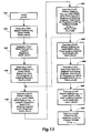
circuitry 128 in Fig. 3 that participate in transfers of data to and from processing units. Fig. 9 shows clock cycles that transfer data from SRAM to a holding register. Fig. 10 shows clock cycles that transfer data from a register in a microprocessor to a holding register. Fig. 11 shows clock cycles that transfer data from a holding register to microprocessor registers. Fig. 12 shows clock cycles that transfer data from a holding register to SRAM. Fig. 13 shows clock cycles in a pipelined transfer of data from SRAM to SRAM. - Fig. 8 shows p processing units, from processing
unit 302 throughprocessing unit 304. Interconnectingcircuitry 128 includes a registered transceiver for each processing unit, from registeredtransceiver 312 to registeredtransceiver 314. The processing units and the respective registered transceivers can be implemented as described above in relation to Fig. 5. - Each processing unit's respective registered transceiver is connected to
common bus 194.Bus 194 can be implemented with conventional 32 bit bus circuitry, and register and decode 154 can provide signals to control data transfer oncommon bus 194 as described below. - Register and decode 154 can select any of several sources for
common bus 194. The sources forcommon bus 194 include registeredtransceivers 312 through 3 14, holdingregister 330, and register and decode 154 throughconstant buffers 192.Common bus 194 can receive from registeredtransceivers 312 through 314 through even and odd buses and transceivers. In addition,common bus 194 can receive from reduction circuitry and from rotation circuitry. Also, when the coprocessor is master ofSBus 102,common bus 194 can receive fromSBus register 188 through registeredtransceiver 122. - Holding
register 330 can be used to store data fromcommon bus 194 during one cycle and then to provide the stored data tocommon bus 194 for transmission to another component during a subsequent cycle. Holdingregister 330 could be implemented with a conventional 32 bit register. Holdingregister 330 can also be implemented in a way that facilitates tiling. The connections between holdingregister 330 andcommon bus 194 can be implemented in a way that facilitates rotation. -
Constant buffers 192 can include two conventional 16 bit buffers. Register and decode 154 can obtain a 32 bit constant in two instructions. In other words, one instruction can include 16 high order bits, and register and decode 154 signals the high order constant buffer to provide the high order bits tocommon bus 194; another instruction can include 16 low order bits, and register and decode 154 signals the low order constant buffer to provide the low order bits tocommon bus 194. When 16 high or low order bits are being provided, the other 16 bits oncommon bus 194 can be pulled to zero by conventional circuitry. Alternatively,constant buffers 192 can include other buffer arrangements, connected to receive a constant of any appropriate width from one or more microinstructions fields of any appropriate width in relation to the constant's width; a 32 bit constant could be loaded, for example, from fields of 4, 8, 16, or 32 bits. - Figs. 9-13 show sequences of microinstructions that can operate the components of Figs. 4, 5, and 8 to perform several data transfers. Each box in Figs. 9-13 represents acts performed during a single clock cycle. In general, the acts that can be completed in a single clock cycle determine which sequences of microinstructions can be executed. For example, an address for
SRAM 240 must be calculated in the clock cycle before it is used, so that the microinstruction specifying the calculation must be fetched fromcontrol store 150 two clock cycles before the address is used. - The pipeline stages for timing calculations can be determined based on which components include a pipeline delay. Signals advance through a pipeline delay only on a rising clock edge. In general, there are no pipeline delays in the control lines from register and decode 154 to other components.
- Each of the following components includes a pipeline delay: registered
transceiver 122;MAR 152; register and decode 154;µPC 166;CMAR 172;registers 174; registered transceiver 186;SBus register 188; internal registers ofmicroprocessors accumulators transceivers 312 through 314; and holdingregister 330. For example, data can be loaded into holdingregister 330 in a first clock cycle; transferred from holdingregister 330 to one of registeredtransceivers 312 through 314 in a second clock cycle; and transferred from one of registeredtransceivers 312 through 314 to a register in a microprocessor in the respective processing unit in a third clock cycle. Similarly, two clock cycles are required for data fromcontrol store 150 to reachSBus 102 through registered transceiver 186 andSBus register 188. - As described above, each microinstruction includes fields specifying address calculation, sequencer operations, and processing unit operations in parallel. Therefore, acts in addition to those shown in Figs. 9-13 could be performed during the same clock cycles in response to appropriate microinstructions. In general, for example, each microinstruction could also specify an operation of
sequencer 160 that loads the address of the next microinstruction to be fetched intoMAR 152. -
Clock cycle 350 in Fig. 9 includes an act that begins a transfer of data fromSRAM 240 to holdingregister 330 by fetching a first microinstruction (µlnst1). µlnst1 includes an address processor instruction that includes an address processor opcode and an address processor register specifier. The instruction, when executed byaddress processor 170, produces an address inSRAM 240 that is loaded intoCMAR 172. -
Clock cycle 352 includes an act that executes µlnst1, providing the address processor instruction to addressprocessor 170 and providing signals so that the address produced byaddress processor 170 is loaded intoCMAR 172.Address processor 170 also executes the address processor instruction duringclock cycle 352.Clock cycle 352 also includes an act that fetches a second microinstruction (ulnst2) whose address was loaded intoMAR 152 duringclock cycle 350. ulnst2 specifies operations that load a data unit from an addressed location inSRAM 240 for each processing unit into its registeredtransceiver 212 by specifying thatSRAM 240 is a source forbuses transceiver 212 should perform a load operation, because registeredtransceiver 212 performs a load operation frombuses SRAM 240 as a source forbuses transceiver 212 could perform a load operation frombuses buses - During
clock cycle 354, the address loaded intoCMAR 172 inclock cycle 352 arrives atSRAM 240.Clock cycle 354 includes an act that executes µlnst2, providing signals that read enable each processing unit'sSRAM 240 so that data units are read from the addressed location and transferred throughbuses transceiver 212, referred to in Figs. 9-13 as "PU Registers."Clock cycle 354 also includes an act that fetches a third microinstruction (ulnst3) whose address was loaded intoMAR 152 duringclock cycle 352. µlnst3 specifies operations that load data units from one of registeredtransceivers 312 through 314 into holdingregister 330, by specifying the registered transceiver of one ofprocessing units 302 through 304 as a source for data oncommon bus 194, and by specifying that holdingregister 330 should perform a load operation. -
Clock cycle 356 includes an act that executes µlnst3, providing signals that select one of registeredtransceivers 312 through 314 as a source and that store data fromcommon bus 194 in holdingregister 330. This clock cycle therefore completes a sequence of microinstructions that transfer data units to holdingregister 330. -
Clock cycle 370 in Fig. 10 includes an act that begins a transfer of data units from microprocessor registers in one ofprocessing units 302 through 304 to holdingregister 330 by fetching a first microinstruction (µlnst1). µlnst1 includes a microprocessor instruction that includes a microprocessor opcode and a microprocessor register specifier. The instruction, when executed by each microprocessor in processingunits 302 through 304, causes each microprocessor to transfer a data unit from the specified register to its accumulator, which always stores the data unit present at the microprocessor's output at the end of every clock cycle. -
Clock cycle 372 includes an act that executes µlnst1, providing the microprocessor instruction to each microprocessor in processingunits 302 through 304. Each microprocessor also executes the instruction duringclock cycle 372, transferring a data unit from the specified register to its accumulator.Clock cycle 372 also includes an act that fetches a second microinstruction (µlnst2) whose address was loaded intoMAR 152 duringclock cycle 370. µlnst2 specifies operations that load data units from theaccumulators transceiver 212, by specifying thataccumulators buses transceiver 212 should perform a load operation, because registeredtransceiver 212 performs a load operation frombuses accumulators buses -
Clock cycle 374 includes an act that executes µlnst2, providing signals toaccumulators buses transceiver 212 so that data units fromaccumulators transceiver 212.Clock cycle 374 also includes an act that fetches a third microinstruction (µlnst3) whose address was loaded intoMAR 152 duringclock cycle 372. µlnst3 specifies operations that load data from one of registeredtransceivers 312 through 314 into holdingregister 330, like the microinstruction fetched duringclock cycle 354 in Fig. 9, described above. -
Clock cycle 376 includes substantially the same act asclock cycle 356 in Fig. 9, described above.Clock cycle 376 therefore completes a sequence of microinstructions that transfer data to holdingregister 330. -
Clock cycle 390 in Fig. 11 includes an act that begins a transfer of data from holdingregister 330 to each processing unit's microprocessors by fetching a first microinstruction (µlnst1). µlnst1 specifies a transfer of data from holdingregister 330 to each of registeredtransceivers 312 through 314 by specifying holdingregister 330 as a source forcommon bus 194.µlnst 1 need not specify that registeredtransceivers 312 through 314 should perform a load operation, because each of registeredtransceivers 312 through 314 performs a load operation during every clock cycle that executes a microinstruction that specifies holdingregister 330 as a source. -
Clock cycle 392 includes an act that executes µlnst1, providing signals so that holdingregister 330 drivescommon bus 194 and registeredtransceivers 312 through 314 load data.Clock cycle 392 also includes an act that fetches a second microinstruction (µlnst2) whose address was loaded intoMAR 152 duringclock cycle 390. µlnst2 includes a microprocessor instruction that includes a microprocessor opcode and a microprocessor register specifier. The instruction, when executed by each microprocessor in processingunits 302 through 304, causes each microprocessor to load data frombus 242 orbus 244 into the specified register. -
Clock cycle 394 includes an act that executes µlnst2, providing signals so that each processing unit's registeredtransceiver 212drives buses units 302 through 304. Each microprocessor also executes the instruction duringclock cycle 394, loading data frombus 242 orbus 244 into the specified register. This clock cycle therefore completes a sequence of microinstructions that transfer data units from holdingregister 330 to a register in each microprocessor in all ofprocessing units 302 through 304. - Fig. 12 illustrates a similar technique to transfer data from holding
register 330 to one or all ofprocessing units 302 through 304.Clock cycle 410 in Fig. 12 includes an act that begins a transfer of data from holdingregister 330 toSRAM 240 of one or all processing units by fetching a first microinstruction (µlnst1). µlnst1 includes an address processor instruction that includes an address processor opcode and an address processor register specifier. The instruction, when executed byaddress processor 170, produces an address inSRAM 240 that is loaded intoCMAR 172. µlnst1 also specifies a transfer of data from holdingregister 330 to each of registeredtransceivers 312 through 314 by specifying holdingregister 330 as a source forcommon bus 194. -
Clock cycle 412 includes an act that executes µlnst1, providing the address processor instruction to addressprocessor 170 and providing signals so that the address produced byaddress processor 170 is loaded intoCMAR 172.Address processor 170 also executes the address processor instruction duringclock cycle 412. The act that executes µlnst1 also provides signals so that holdingregister 330 drivescommon bus 194 and registeredtransceivers 312 through 314 load data.Clock cycle 412 also includes an act that fetches a second microinstruction (µlnst2) whose address was loaded intoMAR 152 duringclock cycle 410. µlnst2 specifies registeredtransceiver 212 as a source forbuses -
Clock cycle 414 includes an act that executes µlnst2, providing signals so that each processing unit's registeredtransceiver 212drives buses transceiver 212 is written as specified. This clock cycle therefore completes a sequence of microinstructions that transfer data units from holdingregister 330 to one or all ofprocessing units 302 through 304. - Register and decode 154 could instead be implemented to permit other write enable selections. For example, a subset of the SRAMs could be write enabled by µlnst2. More generally, a sequence of microinstructions like µlnst 2 could be executed, each with a different specified SRAM, to write an arbitrary subset of SRAMs.
- Acts resembling those in Figs. 11 and 12 could be performed to transfer data through
constant buffers 192 to processing units. Clock cycles 392 and 412 could include, rather than an act transferring data from holdingregister 330 to registeredtransceivers 312 through 314, an act transferring data from register and decode 154 throughconstant buffers 192 to registeredtransceivers 312 through 314. In each case, µlnst1 could specifyconstant buffers 192 as a source forcommon bus 194. If µlnst1 only includes a 16 bit constant, two iterations could be performed to provide one 16 bit constant onbus 242 and another onbus 244; in some cases, the same 16 bit constant could be provided in a single iteration on bothbuses constant buffers 192. - Fig. 13 illustrates a pipelined transfer of data using holding
register 330.Clock cycle 430 in Fig. 13 includes an act that begins a pipelined transfer of data from between SRAMs by fetching a first microinstruction (µlnst1). µlnst1 includes an address processor instruction that includes an address processor opcode and an address processor register specifier. The instruction, when executed byaddress processor 170, produces an address m₀ that is loaded intoCMAR 172. -
Clock cycle 432 includes an act that executes µlnst1, providing the address processor instruction to addressprocessor 170 and providing signals so that address m₀ is loaded intoCMAR 172.Address processor 170 also executes the address processor instruction duringclock cycle 432.Clock cycle 432 also includes an act that fetches a second microinstruction (µlnst2) whose address was loaded intoMAR 152 duringclock cycle 430. µlnst2 specifies operations that load a data unit from an addressed location inSRAM 240 for each processing unit into its registeredtransceiver 212, by specifying thatSRAM 240 is a source forbuses - During
clock cycle 434, address m₀ fromCMAR 172 arrives at each processing unit'sSRAM 240.Clock cycle 434 includes an act that executes µlnst2, providing signals that read enable each processing unit'sSRAM 240 so that data units are read from the location at address m₀ and transferred throughbuses transceiver 212.Clock cycle 434 also includes an act that fetches a third microinstruction (µlnst3) whose address was loaded intoMAR 152 duringclock cycle 432. - Like µlnst1, µlnst3 includes an address processor instruction that produces an address m₁ that is loaded into
CMAR 172. µlnst3 also specifies operations that load data units from one of registeredtransceivers 312 through 314 into holdingregister 330, by specifying the register of one ofprocessing units 302 through 304 as a source for data and by specifying that holdingregister 330 should perform a load operation. -
Clock cycle 436 includes an act that executes µlnst3, providing the address processor instruction to addressprocessor 170 and providing signals so that address m₁ is loaded intoCMAR 172 afteraddress processor 170 executes the address processor instruction. The act of executing µlnst3 also provides signals that select one of registeredtransceivers 312 through 314 as a source and that store data fromcommon bus 194 in holdingregister 330.Clock cycle 436 also includes an act that fetches a fourth microinstruction (µlnst4) wnose address was loaded intoMAR 152 duringclock cycle 434. - Like µlnst2, µlnst4 specifies operations that load a data unit from an addressed location in
SRAM 240 for each processing unit into its registeredtransceiver 212, by specifying thatSRAM 240 is a source forbuses CMAR 172. µlnst4 also specifies a transfer of data from holdingregister 330 to each of registeredtransceivers 312 through 314 by specifying holdingregister 330 as a source forcommon bus 194. - The acts in clock cycles 430, 432, 434, and 436 set up a pipeline that can then be used by iterating the acts in clock cycles 438 and 440. Clock cycles 438 and 440 may be repeated K times, with each iteration being designated as the kth iteration.
-
Clock cycle 438 includes an act that executes µlnst4, providing the address processor instruction to addressprocessor 170 and providing signals so that address n (k - 1) is loaded intoCMAR 172 afteraddress processor 170 executes the address processor instruction. The act that executes µlnst4 also provides signals so that holdingregister 330 drivescommon bus 194 and registeredtransceivers 312 through 314 load data. Like the act inclock cycle 434, the act inclock cycle 438 provides signals that read enable each processing unit'sSRAM 240 so that data units are read from the location at address m (k + 1) and transferred throughbuses transceiver 212.Clock cycle 438 also includes an act that fetches a fifth microinstruction (µlnst5) whose address was loaded intoMAR 152 duringclock cycle 436 or, after the first iteration, duringclock cycle 440 of the previous iteration. - Like µlnst3, µlnst5 includes an address processor instruction that produces an address m (k + 1) that is loaded into
CMAR 172. µlnst5 also specifies operations that load data units from one of registeredtransceivers 312 through 314 into holdingregister 330, by specifying the registered transceiver of one ofprocessing units 302 through 304 as a source for data and by specifying that holdingregister 330 should perform a load operation. µlnst5 also specifies registeredtransceiver 212 as a source forbuses -
Clock cycle 440 includes an act that executes µlnst5, providing the address processor instruction to addressprocessor 170 and providing signals so that address m (k + 1) is loaded intoCMAR 172 afteraddress processor 170 executes the address processor instruction. The act of executing µlnst5 also provides signals that select one of registeredtransceivers 312 through 314 as a source and that store data fromcommon bus 194 in holdingregister 330. The act of executing µlnst5 also provides signals so that each processing unit's registeredtransceiver 212drives buses transceiver 212 is written as specified.Clock cycle 440 also includes an act that either fetches µlnst4 for the next iteration or that fetches a sixth microinstruction (µlnst6), in either case using an address that was loaded intoMAR 152 duringclock cycle 438 of the current iteration. - Like µlnst4, µlnst6 includes an address processor instruction that produces an address n K that is loaded into
CMAR 172. µlnst6 also specifies a transfer of data from holdingregister 330 to each of registeredtransceivers 312 through 314 by specifying holdingregister 330 as a source forcommon bus 194. - The acts in clock cycles 442, 444, 446, and 448 then finish handling the pipeline of data resulting from the preceding steps, but without reading further data from the SRAMs.
-
Clock cycle 442 includes an act that executes µlnsto, providing the address processor instruction to addressprocessor 170 and providing signals so that address n K is loaded intoCMAR 172 afteraddress processor 170 executes the address processor instruction. The act that executes µlnst6 also provides signals so that holdingregister 330 drivescommon bus 194 and registeredtransceivers 312 through 314 load data.Clock cycle 442 also includes an act that fetches a seventh microinstruction (µlnst7) whose address was loaded intoMAR 152 during the Kth iteration ofclock cycle 440 - Like µlnst5, µlnst7 specifies operations that load data units from one of registered
transceivers 312 through 314 into holdingregister 330, by specifying the registered transceiver of one ofprocessing units 302 through 304 as a source and by specifying that holdingregister 330 should perform a load operation. µlnst7 also specifies registeredtransceiver 212 as a source forbuses -
Clock cycle 444 includes an act that executes µlnst7, providing signals that select one of registeredtransceivers 312 through 314 as a source and that store data fromcommon bus 194 in holdingregister 330. The act of executing µlnst7 also provides signals so that each processing unit's registeredtransceiver 212drives buses transceiver 212 is written as specified.Clock cycle 444 also includes an act that fetches an eighth microinstruction (µlnst8), using an address that was loaded intoMAR 152 duringclock cycle 442. - Like µlnst6, µlnst8 includes an address processor instruction that produces an address n (K + 1) that is loaded into
CMAR 172. µlnst8 also specifies a transfer of data from holdingregister 330 to each of registeredtransceivers 312 through 314 by specifying holdingregister 330 as a source forcommon bus 194. -
Clock cycle 446 includes an act that executes µlnst8, providing the address processor instruction to addressprocessor 170 and providing signals so that address n (K + 1) is loaded intoCMAR 172 afteraddress processor 170 executes the address processor instruction. The act that executes µlnst8 also provides signals so that holdingregister 330 drivescommon bus 194 and registeredtransceivers 312 through 314 load data from even and odd buses 320 and 322.Clock cycle 446 also includes an act that fetches a ninth microinstruction (µlnst9) whose address was loaded intoMAR 152 duringclock cycle 444. Like µlnst7, µlnst9 specifies registeredtransceiver 212 as a source forbuses -
Clock cycle 448 includes an act that executes µlnst9, providing signals so that each processing unit's registeredtransceiver 212drives buses transceiver 212 is written as specified. This completes the pipelined transfer of data. - The invention could be applied in many ways, including image processing of the type described in U.S. Patent Nos. US-A 5,065,437; 5,048,109; 5,129,014; and 5,131,049. Such image processing techniques use data defining a first image to obtain a second image through operations such as erosion and dilation, operations that are defined in the Serra books cited above. Such operations can, for example, be performed by a series of suboperations each of which shifts an original image to obtain a shifted image and then performs a Boolean operation with values from the original image and the shifted image at each location. Some parts of the shifting operation can be performed with data transfers implemented as described above.
- The invention could also be applied to perform various other operations, such as pixel counting, gray scale morphology, skew detection, and Boolean operations on images.
- The invention has been described in relation to an implementation with a SPARCStation as a host processor, but the invention could be implemented with any other suitable host processor. More specifically, the invention has been described in relation to a specific clocking scheme and pipelining circuitry appropriate to an SBus, but other clocking schemes and pipelining circuitry could be used as appropriate to other host buses. In addition to the burst transfers described above, concurrent burst transfers in both directions might be implemented with additional pipeline circuitry. Or it might be possible in some implementations for slave and master circuitry to share some components of pipeline circuitry.
- The invention has been described in relation to an implementation in which items of data are transferred in and out of the processing units in horizontal format and operations are performed on items of data in horizontal format. Although this is not necessary and may not be advantageous, the invention might be implemented in a machine that includes corner turning circuitry so that operations can be performed in vertical format and items of data can be stored in vertical format in processing unit memory. Further, the invention might be implemented in a machine in which data can be shifted in and out of a processing unit array. Also, the invention might be implemented with additional circuitry for operating on data relating to an image as it is received from the host bus, such as by subsampling to reduce an image, thereby reducing the amount of data that must be stored in the processing units; this technique would be especially useful in operating on data relating to an image where the data in its original form is larger than the combined memory of the processing units. The invention might also be implemented with circuitry to reorder pixel values or bits within pixel values during a transfer from the host to the coprocessor or from the coprocessor to the host if the representation of data in the the host and coprocessor do not match each other.
- The invention has been described in relation to implementations with conventional microprocessors, but the invention might also be implemented with reduced instruction set (RISC) chips. Such RISC chips do not conventionally have shift inputs and outputs, so that shared memory might be necessary to perform shifting operations between processing units.
- The invention has been described in relation to implementations in which processing units are connected into a one-dimensional array. The invention might also be implemented with a parallel processor in which the processing units are connected into a two- or three-dimensional array or into any other suitable arrangement.
- The invention has been described in relation to implementations in which bits remain uninverted while being transferred between components in a parallel processor. The invention might also be implemented with inversions during data transfer to increase performance, such as an inversion when an item of data is loaded into a holding register and another inversion when the item of data is read out of the holding register.
- The invention has been described in relation to an implementation that inciudes a SIMD parallel processor in which coprocessor control circuitry has two control lines to each processing unit, one to select a register as a source of data on a common bus and the other to write enable the processing unit's memory. The invention might be implemented with other types of parallel processors. For example, the invention could be implemented with additional lines to each processing unit, such as separate instruction and address lines so that each processing unit could operate independently of other processing units. In addition, special write enable lines could be provided to write independently in the memories of different processing units or independently in the memory of a specific microprocessor in each processing unit.
- The invention has been described in relation to implementations in which control circuitry provides addresses in parallel to processing units. The invention might also be implemented witn a parallel processor in which processing units independently obtain addresses, such as from a local address processor or from an address processor that serves a subset of processing units.
- The invention has been described in relation to implementations in which processing units include single port memory circuitry. The invention might also be implemented with dual port memory circuitry.
- The invention has been described in relation to implementations in which a 32 bit bus interconnects 32 bit registers and in which each processing unit includes two 16 bit microprocessors and a 32 bit SRAM. The invention might also be implemented in numerous other ways with components having different widths. For example, each processing unit might include a 16 bit SRAM for each microprocessor or each processing unit might include a single 32 bit microprocessor. Alternatively, the bus might be a 16 bit or 64 bit bus, and other components could be chosen accordingly. Similarly, the control store, described as implemented with 128 bit microinstructions, might also be implemented with microinstructions of other lengths, such as 64 bit encoded microinstructions. Further the invention might be implemented with a aedicated control store chip.
- The invention has been described in relation to implementations that operate on data relating to images, but might also be implemented to operate on data that do not relate to an image.
- The invention has been described in relation to implementations that include readily available discrete components. The invention might also be implemented with custom VLSI components, and similarly with custom memory components.
- The invention has been described in relation to implementations in which each processing unit includes SRAM, but the invention might also be implemented with other types of memory, such as dynamic RAM, flash RAM, and so forth.
Claims (10)
- A parallel processor comprising:
a plurality of processing units (12,14,16);
interconnecting circuitry for interconnecting the processing units; the interconnecting circuitry comprising:
bus circuitry (30);
for each processing unit, respective source/destination circuitry (32,34,36) connected to the bus circuitry (30) and the processing unit (12,14,16) for providing items of data from the processing unit to the bus circuitry and for receiving items of data from the bus circuitry for the processing unit; and
a transfer register (38) connected to the bus circuitry for receiving items of data from the bus circuitry, for storing received items of data, and for providing stored items of data to the bus circuitry; the bus circuitry being capable of transferring an item of data received from the source/destination circuitry (32,34,36) of each of the processing units (12,14,16) to the transfer register (38) and further being capable of transferring an item of data received from the transfer register to the source/destination circuitry of each of the processing units; and control circuitry (44) connected for controlling the processing units and the interconnecting circuitry; the control circuitry comprising transfer control circuitry connected for providing signals to each processing unit's source/destination circuitry (32,34,36) and to the transfer register to control transfer of data by the bus circuitry and storing of data in the transfer register. - A parallel processor comprising:
a plurality of processing units;
interconnecting circuitry for interconnecting the processing units; the interconnecting circuitry comprising:
bus circuitry; and
for each processing unit, respective destination circuitry connected to the bus circuitry and the processing unit for receiving items of data from the bus for the processing unit; and
control circuitry connected for controlling the processing units and the interconnecting circuitry; the control circuitry comprising:
value source circuitry connected to the bus for providing items of data to the bus circuitry, each item of data indicating a respective value; the bus circuitry being capable of transferring an item of data received from the value source circuitry to the destination circuitry of each of the processing units; and
transfer control circuitry connected for providing signals to each processing unit's destination circuitry to control transfers of data by the bus circuitry. - The parallel processor of claim 1 or claim 2 in which the interconnecting circuitry further comprises for pairs of the processing units, respective pair transfer circuitry for transferring items of data from either of the processing units in the pair to the other processing unit in the pair; the pair transfer circuitry of all of the pairs of processing units together interconnecting the processing units into an array.
- The parallel processor of claim 1 in which the transfer control circuitry comprises source select circuitry for selecting one of the processing units to provide a data item to the bus circuitry.
- The parallel processor of claim 1 or claim 2 in which the transfer control circuitry comprises destination select circuitry for selecting each of a set of the processing units to receive a data item from the bus circuitry.
- The parallel processor of claim 1 or claim 2 in which each processing unit comprises processing circuitry for responding to instructions by performing operations on items of data; the processing circuitry of each processing unit being connected to receive a data item from the processing unit's source/destination circuitry or destination circuitry; the processing circuitry comprising an internal register;
the control circuitry further comprising instruction circuitry for providing a series of items of instruction data to the processing circuitry of each of the processing units; the items of instruction data indicating a sequence of instructions; the instruction circuitry being connected for providing each item in the series to the processing circuitry of all of the processing units in parallel;
the processing circuitry of all of the processing units receiving a load instruction from the instruction circuitry in parallel; the processing circuitry responding to the load instruction by loading a data item from the source/destination circuitry or destination circuitry into the internal register so that the data item is stored in the internal register of the processing circuitry in all the processing units. - A method of operating a parallel processor that includes:
a plurality of processing units; and
interconnecting circuitry for interconnecting the processing units; the interconnecting circuitry including:
bus circuitry;
for each processing unit, respective source/destination circuitry connected to the bus circuitry and the processing unit for providing items of data from the processing unit to the bus circuitry and for receiving items of data from the bus circuitry for the processing unit; and
a transfer register connected to the bus circuitry for receiving items of data from the bus circuitry, for storing received items of data, and for providing stored items of data to the bus circuitry; the bus circuitry being capable of transferring an item of data received from the source/destination circuitry of each of the processing units to the transfer register and further being capable of transferring an item of data received from the transfer register to the source/destination circuitry of each of the processing units; and
the method comprising acts of:
providing signals to the source/destination circuitry of one of the processing units so that the source/destination circuitry receives an item of data from the processing unit;
providing signals to the source/destination circuitry of the one of the processing units so that the source/destination circuitry provides the item of data to the bus circuitry; and
providing signals to the transfer register so that the transfer register receives the item of data from the bus circuitry and stores the item of data. - A method of operating a parallel processor that includes:
a plurality of processing units; each processing unit comprising processing circuitry for responding to instructions by performing operations on items of data;
interconnecting circuitry for interconnecting the processing units; the interconnecting circuitry including:bus circuitry;
for each processing unit, respective source/destination circuitry connected to the bus circuitry and the processing unit for providing items of data trom the processing unit to the bus circuitry and for receiving items of data from the bus circuitry for the processing unit; and
a transter register connected to the bus circuitry for receiving items of data from the bus circuitry, for storing received items of data, and for providing stored items of data to the bus circuitry; the bus circuitry being capable of transferring an item of data received from the source/destination circuitry of each of the processing units to the transfer register and further being capable of transferring an item of data received from the transfer register to the source/destination circuitry of each of the processing units;
instruction circuitry for providing a series of items of instruction data to the processing circuitry of each of the processing units; the items of instruction data indicating a sequence of instructions; the instruction circuitry being connected for providing each item in the series to the processing circuitry of all of the processing units in parallel;
the method comprising acts of:
providing signals to the transfer register so that the transfer register provides a stored item of data to the bus circuitry;
providing signals to the source/destination circuitry of each processing unit in a set of the processing units so that the source/destination circuitry of each processing unit in the set receives the item of data from the bus circuitry; and
providing signals to the source/destination circuitry of each processing unit in the set so that the source/destination circuitry of each processing unit in the set provides the item of data to its processing unit. - A method of operating a parallel processor that includes:
a plurality of processing units;
interconnecting circuitry for interconnecting the processing units; the interconnecting circuitry including:
bus circuitry;
for each processing unit, respective source/destination circuitry connected to the bus circuitry and the processing unit for providing items of data from the processing unit to the bus circuitry and for receiving items of data from the bus circuitry for the processing unit; and
a transfer register connected to the bus circuitry for receiving items of data from the bus circuitry, for storing received items of data, and for providing stored items of data to the bus circuitry; the bus circuitry being capable of transferring an item of data received from the source/destination circuitry of each of the processing units to the transfer register and further being capable of transferring an item of data received from the transfer register to the source/destination circuitry of each of the processing units;
the method comprising a first act and a sequence of following acts ; each following act having a respective preceding act in the sequence that it follows; each following act comprising a respective first subact and a respective second subact;
each following act's first subact comprising:
providing signals to the source/destination circuitry of one of the processing units so that the source/destination circuitry receives a first item of data from the processing unit;
providing signals to the transfer register so that the transfer register provides a second item of data to the bus circuitry; the second item of data being received by the transfer register during the following act's preceding act; and
providing signals to the source/destination circuitry of each processing unit in a set of the processing units so that the source/destination circuitry of each processing unit in the set receives the second item of data from the bus circuitry;
each following act's second subact comprising:
providing signals to the source/destination circuitry of the one of the processing units so that the source/destination circuitry provides the first item of data to the bus circuitry;
providing signals to the transfer register so that the transfer register receives the first item of data from the bus circuitry and stores the first item of data; and
providing signals to the source/destination circuitry of each processing unit in the set so that the source/destination circuitry of each processing unit in the set provides the second item of data to its processing unit. - A method of operating a parallel processor that includes:
a plurality of processing units;
interconnecting circuitry for interconnecting the processing units; the interconnecting circuitry including:
bus circuitry; and
for each processing unit, respective destination circuitry connected to the bus circuitry and the processing unit for receiving items of data from the bus circuitry for the processing unit;
the method comprising acts of:
providing an item of data to the bus circuitry, the item of data indicating a respective value; the bus circuitry being capable of transferring the item of data to the destination circuitry of each of the processing units;
providing signals to the destination circuitry of each processing unit in a set of the processing units so that the destination circuitry of each processing unit in the set receives the item of data from the bus circuitry; and
providing signals to the destination circuitry of each processing unit in the set so that the destination circuitry of each processing unit in the set provides the item of data to its processing unit.
Applications Claiming Priority (2)
| Application Number | Priority Date | Filing Date | Title |
|---|---|---|---|
| US07/993,218 US5450603A (en) | 1992-12-18 | 1992-12-18 | SIMD architecture with transfer register or value source circuitry connected to bus |
| US993218 | 1992-12-18 |
Publications (3)
| Publication Number | Publication Date |
|---|---|
| EP0602909A2 true EP0602909A2 (en) | 1994-06-22 |
| EP0602909A3 EP0602909A3 (en) | 1994-07-06 |
| EP0602909B1 EP0602909B1 (en) | 1999-11-10 |
Family
ID=25539256
Family Applications (1)
| Application Number | Title | Priority Date | Filing Date |
|---|---|---|---|
| EP93309971A Expired - Lifetime EP0602909B1 (en) | 1992-12-18 | 1993-12-10 | SIMD architecture with bus for transferring data to and from processing units |
Country Status (4)
| Country | Link |
|---|---|
| US (1) | US5450603A (en) |
| EP (1) | EP0602909B1 (en) |
| JP (1) | JPH06223209A (en) |
| DE (1) | DE69326986T2 (en) |
Cited By (5)
| Publication number | Priority date | Publication date | Assignee | Title |
|---|---|---|---|---|
| EP0726532A2 (en) * | 1995-02-10 | 1996-08-14 | International Business Machines Corporation | Array processor communication architecture with broadcast instuctions |
| GB2352306A (en) * | 1999-04-09 | 2001-01-24 | Pixelfusion Ltd | Parallel processing apparatus using a SIMD array |
| US7506136B2 (en) | 1999-04-09 | 2009-03-17 | Clearspeed Technology Plc | Parallel data processing apparatus |
| US7526630B2 (en) | 1999-04-09 | 2009-04-28 | Clearspeed Technology, Plc | Parallel data processing apparatus |
| US7627736B2 (en) | 1999-04-09 | 2009-12-01 | Clearspeed Technology Plc | Thread manager to control an array of processing elements |
Families Citing this family (50)
| Publication number | Priority date | Publication date | Assignee | Title |
|---|---|---|---|---|
| US5354695A (en) * | 1992-04-08 | 1994-10-11 | Leedy Glenn J | Membrane dielectric isolation IC fabrication |
| US5655131A (en) * | 1992-12-18 | 1997-08-05 | Xerox Corporation | SIMD architecture for connection to host processor's bus |
| US5651121A (en) * | 1992-12-18 | 1997-07-22 | Xerox Corporation | Using mask operand obtained from composite operand to perform logic operation in parallel with composite operand |
| DE4344157A1 (en) * | 1993-12-23 | 1995-06-29 | Philips Patentverwaltung | Radio |
| US5557734A (en) * | 1994-06-17 | 1996-09-17 | Applied Intelligent Systems, Inc. | Cache burst architecture for parallel processing, such as for image processing |
| US5754590A (en) * | 1996-05-17 | 1998-05-19 | Lucent Technologies, Inc. | Modem architecture for integrated controller and data pump applications |
| US6551857B2 (en) | 1997-04-04 | 2003-04-22 | Elm Technology Corporation | Three dimensional structure integrated circuits |
| JPH1115773A (en) * | 1997-06-24 | 1999-01-22 | Matsushita Electron Corp | Semiconductor integrated circuit, computer system, data processor and data processing method |
| KR100538605B1 (en) | 1998-03-18 | 2005-12-22 | 코닌클리즈케 필립스 일렉트로닉스 엔.브이. | Data processing device and method of computing the cosine transform of a matrix |
| US6219733B1 (en) | 1998-08-26 | 2001-04-17 | International Business Machines Corporation | Transmission line loop |
| ATE396449T1 (en) | 1999-09-01 | 2008-06-15 | Intel Corp | REGISTER SET FOR USE IN A PARALLEL MULTI-WIRE PROCESSOR ARCHITECTURE |
| WO2001016702A1 (en) | 1999-09-01 | 2001-03-08 | Intel Corporation | Register set used in multithreaded parallel processor architecture |
| JP3971535B2 (en) * | 1999-09-10 | 2007-09-05 | 株式会社リコー | SIMD type processor |
| US7681018B2 (en) * | 2000-08-31 | 2010-03-16 | Intel Corporation | Method and apparatus for providing large register address space while maximizing cycletime performance for a multi-threaded register file set |
| US20020053017A1 (en) * | 2000-09-01 | 2002-05-02 | Adiletta Matthew J. | Register instructions for a multithreaded processor |
| US7487505B2 (en) | 2001-08-27 | 2009-02-03 | Intel Corporation | Multithreaded microprocessor with register allocation based on number of active threads |
| US6868476B2 (en) | 2001-08-27 | 2005-03-15 | Intel Corporation | Software controlled content addressable memory in a general purpose execution datapath |
| US7216204B2 (en) | 2001-08-27 | 2007-05-08 | Intel Corporation | Mechanism for providing early coherency detection to enable high performance memory updates in a latency sensitive multithreaded environment |
| US7225281B2 (en) * | 2001-08-27 | 2007-05-29 | Intel Corporation | Multiprocessor infrastructure for providing flexible bandwidth allocation via multiple instantiations of separate data buses, control buses and support mechanisms |
| US8149904B2 (en) * | 2002-01-24 | 2012-04-03 | Broadcom Corporation | Asymmetric digital subscriber line modem apparatus and methods therefor |
| US7610451B2 (en) | 2002-01-25 | 2009-10-27 | Intel Corporation | Data transfer mechanism using unidirectional pull bus and push bus |
| US6806737B2 (en) * | 2002-03-21 | 2004-10-19 | Raymond Jit-Hung Sung | Bi-directional amplifier and method for accelerated bus line communication |
| US6803782B2 (en) * | 2002-03-21 | 2004-10-12 | John Conrad Koob | Arrayed processing element redundancy architecture |
| US7437724B2 (en) * | 2002-04-03 | 2008-10-14 | Intel Corporation | Registers for data transfers |
| WO2004015764A2 (en) | 2002-08-08 | 2004-02-19 | Leedy Glenn J | Vertical system integration |
| US7337275B2 (en) * | 2002-08-13 | 2008-02-26 | Intel Corporation | Free list and ring data structure management |
| US7133563B2 (en) | 2002-10-31 | 2006-11-07 | Microsoft Corporation | Passive embedded interaction code |
| US7116840B2 (en) | 2002-10-31 | 2006-10-03 | Microsoft Corporation | Decoding and error correction in 2-D arrays |
| US6941438B2 (en) | 2003-01-10 | 2005-09-06 | Intel Corporation | Memory interleaving |
| US7583842B2 (en) | 2004-01-06 | 2009-09-01 | Microsoft Corporation | Enhanced approach of m-array decoding and error correction |
| US7263224B2 (en) | 2004-01-16 | 2007-08-28 | Microsoft Corporation | Strokes localization by m-array decoding and fast image matching |
| US7607076B2 (en) | 2005-02-18 | 2009-10-20 | Microsoft Corporation | Embedded interaction code document |
| US7826074B1 (en) | 2005-02-25 | 2010-11-02 | Microsoft Corporation | Fast embedded interaction code printing with custom postscript commands |
| US7599560B2 (en) | 2005-04-22 | 2009-10-06 | Microsoft Corporation | Embedded interaction code recognition |
| US7542976B2 (en) * | 2005-04-22 | 2009-06-02 | Microsoft Corporation | Local metadata embedding and decoding |
| US7421439B2 (en) | 2005-04-22 | 2008-09-02 | Microsoft Corporation | Global metadata embedding and decoding |
| US7400777B2 (en) | 2005-05-25 | 2008-07-15 | Microsoft Corporation | Preprocessing for information pattern analysis |
| US7729539B2 (en) | 2005-05-31 | 2010-06-01 | Microsoft Corporation | Fast error-correcting of embedded interaction codes |
| US7580576B2 (en) | 2005-06-02 | 2009-08-25 | Microsoft Corporation | Stroke localization and binding to electronic document |
| US7619607B2 (en) | 2005-06-30 | 2009-11-17 | Microsoft Corporation | Embedding a pattern design onto a liquid crystal display |
| US7817816B2 (en) | 2005-08-17 | 2010-10-19 | Microsoft Corporation | Embedded interaction code enabled surface type identification |
| US7622182B2 (en) | 2005-08-17 | 2009-11-24 | Microsoft Corporation | Embedded interaction code enabled display |
| JP4720436B2 (en) * | 2005-11-01 | 2011-07-13 | 株式会社日立製作所 | Reconfigurable processor or device |
| US7584342B1 (en) * | 2005-12-15 | 2009-09-01 | Nvidia Corporation | Parallel data processing systems and methods using cooperative thread arrays and SIMD instruction issue |
| US7861060B1 (en) | 2005-12-15 | 2010-12-28 | Nvidia Corporation | Parallel data processing systems and methods using cooperative thread arrays and thread identifier values to determine processing behavior |
| US7788468B1 (en) | 2005-12-15 | 2010-08-31 | Nvidia Corporation | Synchronization of threads in a cooperative thread array |
| CN102508643A (en) * | 2011-11-16 | 2012-06-20 | 刘大可 | Multicore-parallel digital signal processor and method for operating parallel instruction sets |
| US9262704B1 (en) * | 2015-03-04 | 2016-02-16 | Xerox Corporation | Rendering images to lower bits per pixel formats using reduced numbers of registers |
| JP6627630B2 (en) * | 2016-04-15 | 2020-01-08 | 富士通株式会社 | Compilation method, compilation program and information processing device |
| CN113867789A (en) * | 2020-06-30 | 2021-12-31 | 上海寒武纪信息科技有限公司 | Computing device, integrated circuit chip, board card, electronic equipment and computing method |
Citations (3)
| Publication number | Priority date | Publication date | Assignee | Title |
|---|---|---|---|---|
| EP0147851A2 (en) * | 1983-12-29 | 1985-07-10 | CHINOIN Gyogyszer és Vegyészeti Termékek Gyára RT. | Water soluble forms of polyene antibiotics, and process for preparing them |
| EP0236762A1 (en) * | 1986-03-08 | 1987-09-16 | Hitachi, Ltd. | Multiprocessor system |
| JPS63276659A (en) * | 1987-03-27 | 1988-11-14 | Nec Corp | Composite computer system |
Family Cites Families (18)
| Publication number | Priority date | Publication date | Assignee | Title |
|---|---|---|---|---|
| US4204251A (en) * | 1977-12-28 | 1980-05-20 | Finn Brudevold | Interconnection unit for multiple data processing systems |
| JPS56164464A (en) * | 1980-05-21 | 1981-12-17 | Tatsuo Nogi | Parallel processing computer |
| US4745546A (en) * | 1982-06-25 | 1988-05-17 | Hughes Aircraft Company | Column shorted and full array shorted functional plane for use in a modular array processor and method for using same |
| WO1984004638A1 (en) * | 1983-05-12 | 1984-11-22 | American Telephone & Telegraph | Communication network |
| US4814973A (en) * | 1983-05-31 | 1989-03-21 | Hillis W Daniel | Parallel processor |
| JPH0642237B2 (en) * | 1983-12-28 | 1994-06-01 | 株式会社日立製作所 | Parallel processor |
| US4850027A (en) * | 1985-07-26 | 1989-07-18 | International Business Machines Corporation | Configurable parallel pipeline image processing system |
| US4831519A (en) * | 1985-12-12 | 1989-05-16 | Itt Corporation | Cellular array processor with variable nesting depth vector control by selective enabling of left and right neighboring processor cells |
| US4984235A (en) * | 1987-04-27 | 1991-01-08 | Thinking Machines Corporation | Method and apparatus for routing message packets and recording the roofing sequence |
| US5129092A (en) * | 1987-06-01 | 1992-07-07 | Applied Intelligent Systems,Inc. | Linear chain of parallel processors and method of using same |
| DE3851005T2 (en) * | 1987-06-01 | 1995-04-20 | Applied Intelligent Syst Inc | Parallel neighboring processing system and method. |
| US5297255A (en) * | 1987-07-28 | 1994-03-22 | Hitachi, Ltd. | Parallel computer comprised of processor elements having a local memory and an enhanced data transfer mechanism |
| US5113510A (en) * | 1987-12-22 | 1992-05-12 | Thinking Machines Corporation | Method and apparatus for operating a cache memory in a multi-processor |
| US5148547A (en) * | 1988-04-08 | 1992-09-15 | Thinking Machines Corporation | Method and apparatus for interfacing bit-serial parallel processors to a coprocessor |
| US5268856A (en) * | 1988-06-06 | 1993-12-07 | Applied Intelligent Systems, Inc. | Bit serial floating point parallel processing system and method |
| US5280547A (en) * | 1990-06-08 | 1994-01-18 | Xerox Corporation | Dense aggregative hierarhical techniques for data analysis |
| US5325500A (en) * | 1990-12-14 | 1994-06-28 | Xerox Corporation | Parallel processing units on a substrate, each including a column of memory |
| US5148500A (en) * | 1991-01-24 | 1992-09-15 | Aoi Systems, Inc. | Morphological processing system |
-
1992
- 1992-12-18 US US07/993,218 patent/US5450603A/en not_active Expired - Fee Related
-
1993
- 1993-12-10 EP EP93309971A patent/EP0602909B1/en not_active Expired - Lifetime
- 1993-12-10 DE DE69326986T patent/DE69326986T2/en not_active Expired - Fee Related
- 1993-12-14 JP JP5313843A patent/JPH06223209A/en active Pending
Patent Citations (3)
| Publication number | Priority date | Publication date | Assignee | Title |
|---|---|---|---|---|
| EP0147851A2 (en) * | 1983-12-29 | 1985-07-10 | CHINOIN Gyogyszer és Vegyészeti Termékek Gyára RT. | Water soluble forms of polyene antibiotics, and process for preparing them |
| EP0236762A1 (en) * | 1986-03-08 | 1987-09-16 | Hitachi, Ltd. | Multiprocessor system |
| JPS63276659A (en) * | 1987-03-27 | 1988-11-14 | Nec Corp | Composite computer system |
Non-Patent Citations (1)
| Title |
|---|
| PATENT ABSTRACTS OF JAPAN vol. 13, no. 96 (P-839)(3444) 7 March 1989 & JP-A-63 276 659 (N.E.C. CORP) 14 November 1988 * |
Cited By (7)
| Publication number | Priority date | Publication date | Assignee | Title |
|---|---|---|---|---|
| EP0726532A2 (en) * | 1995-02-10 | 1996-08-14 | International Business Machines Corporation | Array processor communication architecture with broadcast instuctions |
| EP0726532A3 (en) * | 1995-02-10 | 1997-03-19 | Ibm | Array processor communication architecture with broadcast instuctions |
| US5659785A (en) * | 1995-02-10 | 1997-08-19 | International Business Machines Corporation | Array processor communication architecture with broadcast processor instructions |
| GB2352306A (en) * | 1999-04-09 | 2001-01-24 | Pixelfusion Ltd | Parallel processing apparatus using a SIMD array |
| US7506136B2 (en) | 1999-04-09 | 2009-03-17 | Clearspeed Technology Plc | Parallel data processing apparatus |
| US7526630B2 (en) | 1999-04-09 | 2009-04-28 | Clearspeed Technology, Plc | Parallel data processing apparatus |
| US7627736B2 (en) | 1999-04-09 | 2009-12-01 | Clearspeed Technology Plc | Thread manager to control an array of processing elements |
Also Published As
| Publication number | Publication date |
|---|---|
| EP0602909B1 (en) | 1999-11-10 |
| DE69326986T2 (en) | 2000-04-27 |
| US5450603A (en) | 1995-09-12 |
| DE69326986D1 (en) | 1999-12-16 |
| JPH06223209A (en) | 1994-08-12 |
| EP0602909A3 (en) | 1994-07-06 |
Similar Documents
| Publication | Publication Date | Title |
|---|---|---|
| EP0602909B1 (en) | SIMD architecture with bus for transferring data to and from processing units | |
| US5437045A (en) | Parallel processing with subsampling/spreading circuitry and data transfer circuitry to and from any processing unit | |
| EP0602915B1 (en) | SIMD architecture for connection to host processor's bus | |
| US4873626A (en) | Parallel processing system with processor array having memory system included in system memory | |
| US5165023A (en) | Parallel processing system with processor array and network communications system for transmitting messages of variable length | |
| US4891787A (en) | Parallel processing system with processor array having SIMD/MIMD instruction processing | |
| US6260088B1 (en) | Single integrated circuit embodying a risc processor and a digital signal processor | |
| US5559951A (en) | Page printer controller including a single chip superscalar microprocessor with graphics functional units | |
| US5872987A (en) | Massively parallel computer including auxiliary vector processor | |
| US5606520A (en) | Address generator with controllable modulo power of two addressing capability | |
| US5968167A (en) | Multi-threaded data processing management system | |
| US6038584A (en) | Synchronized MIMD multi-processing system and method of operation | |
| US5961628A (en) | Load and store unit for a vector processor | |
| US5418970A (en) | Parallel processing system with processor array with processing elements addressing associated memories using host supplied address value and base register content | |
| US4509116A (en) | Special instruction processing unit for data processing system | |
| JPH06149545A (en) | Semiconductor integrated circuit provided with cpu and multiplier | |
| US5450604A (en) | Data rotation using parallel to serial units that receive data from memory units and rotation buffer that provides rotated data to memory units | |
| WO2001084297A2 (en) | Flexible and efficient processor for use in image processing | |
| EP0036185A2 (en) | Information processing system incorporating 1-chip arithmetic control unit of very large scale integrated semiconductor element | |
| KR20010031192A (en) | Data processing system for logically adjacent data samples such as image data in a machine vision system | |
| US5428804A (en) | Edge crossing circuitry for SIMD architecture | |
| KR940011594B1 (en) | Multiprocessor controller having time shared control store | |
| US6728741B2 (en) | Hardware assist for data block diagonal mirror image transformation | |
| JP3128799B2 (en) | Data processing device, data processing system, and outline font data generation method | |
| JP2680828B2 (en) | Digital device |
Legal Events
| Date | Code | Title | Description |
|---|---|---|---|
| PUAI | Public reference made under article 153(3) epc to a published international application that has entered the european phase |
Free format text: ORIGINAL CODE: 0009012 |
|
| PUAL | Search report despatched |
Free format text: ORIGINAL CODE: 0009013 |
|
| AK | Designated contracting states |
Kind code of ref document: A2 Designated state(s): DE FR GB |
|
| AK | Designated contracting states |
Kind code of ref document: A3 Designated state(s): DE FR GB |
|
| 17P | Request for examination filed |
Effective date: 19950109 |
|
| 17Q | First examination report despatched |
Effective date: 19970611 |
|
| GRAG | Despatch of communication of intention to grant |
Free format text: ORIGINAL CODE: EPIDOS AGRA |
|
| GRAG | Despatch of communication of intention to grant |
Free format text: ORIGINAL CODE: EPIDOS AGRA |
|
| GRAH | Despatch of communication of intention to grant a patent |
Free format text: ORIGINAL CODE: EPIDOS IGRA |
|
| GRAH | Despatch of communication of intention to grant a patent |
Free format text: ORIGINAL CODE: EPIDOS IGRA |
|
| GRAA | (expected) grant |
Free format text: ORIGINAL CODE: 0009210 |
|
| AK | Designated contracting states |
Kind code of ref document: B1 Designated state(s): DE FR GB |
|
| REF | Corresponds to: |
Ref document number: 69326986 Country of ref document: DE Date of ref document: 19991216 |
|
| ET | Fr: translation filed | ||
| PLBE | No opposition filed within time limit |
Free format text: ORIGINAL CODE: 0009261 |
|
| STAA | Information on the status of an ep patent application or granted ep patent |
Free format text: STATUS: NO OPPOSITION FILED WITHIN TIME LIMIT |
|
| 26N | No opposition filed | ||
| REG | Reference to a national code |
Ref country code: GB Ref legal event code: IF02 |
|
| PGFP | Annual fee paid to national office [announced via postgrant information from national office to epo] |
Ref country code: DE Payment date: 20041202 Year of fee payment: 12 |
|
| PGFP | Annual fee paid to national office [announced via postgrant information from national office to epo] |
Ref country code: GB Payment date: 20041208 Year of fee payment: 12 |
|
| PGFP | Annual fee paid to national office [announced via postgrant information from national office to epo] |
Ref country code: FR Payment date: 20050825 Year of fee payment: 13 |
|
| PG25 | Lapsed in a contracting state [announced via postgrant information from national office to epo] |
Ref country code: GB Free format text: LAPSE BECAUSE OF NON-PAYMENT OF DUE FEES Effective date: 20051210 |
|
| PG25 | Lapsed in a contracting state [announced via postgrant information from national office to epo] |
Ref country code: DE Free format text: LAPSE BECAUSE OF NON-PAYMENT OF DUE FEES Effective date: 20060701 |
|
| GBPC | Gb: european patent ceased through non-payment of renewal fee |
Effective date: 20051210 |
|
| REG | Reference to a national code |
Ref country code: FR Ref legal event code: ST Effective date: 20070831 |
|
| PG25 | Lapsed in a contracting state [announced via postgrant information from national office to epo] |
Ref country code: FR Free format text: LAPSE BECAUSE OF NON-PAYMENT OF DUE FEES Effective date: 20070102 |