EP0602872A2 - Beam reprofiling by binary diffraction optics - Google Patents
Beam reprofiling by binary diffraction optics Download PDFInfo
- Publication number
- EP0602872A2 EP0602872A2 EP93309795A EP93309795A EP0602872A2 EP 0602872 A2 EP0602872 A2 EP 0602872A2 EP 93309795 A EP93309795 A EP 93309795A EP 93309795 A EP93309795 A EP 93309795A EP 0602872 A2 EP0602872 A2 EP 0602872A2
- Authority
- EP
- European Patent Office
- Prior art keywords
- light beam
- binary diffraction
- intensity
- optic lens
- diffraction optic
- Prior art date
- Legal status (The legal status is an assumption and is not a legal conclusion. Google has not performed a legal analysis and makes no representation as to the accuracy of the status listed.)
- Ceased
Links
Images


Classifications
-
- G—PHYSICS
- G02—OPTICS
- G02B—OPTICAL ELEMENTS, SYSTEMS OR APPARATUS
- G02B27/00—Optical systems or apparatus not provided for by any of the groups G02B1/00 - G02B26/00, G02B30/00
- G02B27/42—Diffraction optics, i.e. systems including a diffractive element being designed for providing a diffractive effect
- G02B27/4205—Diffraction optics, i.e. systems including a diffractive element being designed for providing a diffractive effect having a diffractive optical element [DOE] contributing to image formation, e.g. whereby modulation transfer function MTF or optical aberrations are relevant
- G02B27/4227—Diffraction optics, i.e. systems including a diffractive element being designed for providing a diffractive effect having a diffractive optical element [DOE] contributing to image formation, e.g. whereby modulation transfer function MTF or optical aberrations are relevant in image scanning systems
-
- G—PHYSICS
- G02—OPTICS
- G02B—OPTICAL ELEMENTS, SYSTEMS OR APPARATUS
- G02B27/00—Optical systems or apparatus not provided for by any of the groups G02B1/00 - G02B26/00, G02B30/00
- G02B27/0025—Optical systems or apparatus not provided for by any of the groups G02B1/00 - G02B26/00, G02B30/00 for optical correction, e.g. distorsion, aberration
- G02B27/0037—Optical systems or apparatus not provided for by any of the groups G02B1/00 - G02B26/00, G02B30/00 for optical correction, e.g. distorsion, aberration with diffracting elements
-
- G—PHYSICS
- G02—OPTICS
- G02B—OPTICAL ELEMENTS, SYSTEMS OR APPARATUS
- G02B27/00—Optical systems or apparatus not provided for by any of the groups G02B1/00 - G02B26/00, G02B30/00
- G02B27/42—Diffraction optics, i.e. systems including a diffractive element being designed for providing a diffractive effect
- G02B27/4233—Diffraction optics, i.e. systems including a diffractive element being designed for providing a diffractive effect having a diffractive element [DOE] contributing to a non-imaging application
- G02B27/4244—Diffraction optics, i.e. systems including a diffractive element being designed for providing a diffractive effect having a diffractive element [DOE] contributing to a non-imaging application in wavelength selecting devices
-
- G—PHYSICS
- G02—OPTICS
- G02B—OPTICAL ELEMENTS, SYSTEMS OR APPARATUS
- G02B27/00—Optical systems or apparatus not provided for by any of the groups G02B1/00 - G02B26/00, G02B30/00
- G02B27/42—Diffraction optics, i.e. systems including a diffractive element being designed for providing a diffractive effect
- G02B27/4233—Diffraction optics, i.e. systems including a diffractive element being designed for providing a diffractive effect having a diffractive element [DOE] contributing to a non-imaging application
- G02B27/425—Diffraction optics, i.e. systems including a diffractive element being designed for providing a diffractive effect having a diffractive element [DOE] contributing to a non-imaging application in illumination systems
-
- G—PHYSICS
- G02—OPTICS
- G02B—OPTICAL ELEMENTS, SYSTEMS OR APPARATUS
- G02B27/00—Optical systems or apparatus not provided for by any of the groups G02B1/00 - G02B26/00, G02B30/00
- G02B27/42—Diffraction optics, i.e. systems including a diffractive element being designed for providing a diffractive effect
- G02B27/4272—Diffraction optics, i.e. systems including a diffractive element being designed for providing a diffractive effect having plural diffractive elements positioned sequentially along the optical path
- G02B27/4277—Diffraction optics, i.e. systems including a diffractive element being designed for providing a diffractive effect having plural diffractive elements positioned sequentially along the optical path being separated by an air space
-
- G—PHYSICS
- G02—OPTICS
- G02B—OPTICAL ELEMENTS, SYSTEMS OR APPARATUS
- G02B27/00—Optical systems or apparatus not provided for by any of the groups G02B1/00 - G02B26/00, G02B30/00
- G02B27/09—Beam shaping, e.g. changing the cross-sectional area, not otherwise provided for
- G02B27/0938—Using specific optical elements
- G02B27/0944—Diffractive optical elements, e.g. gratings, holograms
Definitions
- This invention relates to a raster scanner in which the intensity of a light beam is reprofiled across its width.
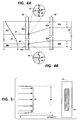
- a conventional raster scanner system utilizes a light source 12, a modulator 14, a multi-faceted rotating polygon mirror 16 as the scanning element and a photosensitive medium 18.
- the modulator 14 receives pixel information and modulates the light beam 20 in accordance with the pixel information.
- the raster scanner system utilizes overfill scanning and therefore, the modulated light beam 20 will be directed onto two facets 22 of the rotating polygon mirror 16.
- the rotating polygon mirror 16 reflects the light beam 20 and also causes the reflected light 20 to revolve about an axis near the center of rotation of the rotating polygon 16 and scans a line. This reflected light beam 20 can be utilized to impinge upon a photographic film or a photosensitive medium 18, such as a xerographic drum at the output of the imaging system.
- a laser light beam has a Gaussian distribution 30 which has a maximum intensity at the center C of the beam and a gradually decreasing intensity towards the outer shell S of the beam.
- an electro-optic crystal 14a used in the modulator 14 should be wide enough to encompass the width w of the light beam.
- the intensity of the light beam varies from the center C of the beam to the outer shell 5
- the surface of the electro-optic crystal 14a of the modulator 14 does not receive a uniform intensity.
- the center portion Ca of the electro-optic crystal is exposed to the maximum intensity from the center C of the light beam and the rest of the electro-optic crystal is exposed to less intensity.
- the non-uniform light excites carriers from impurities such as iron in the crystal. These carriers move in the crystal by diffusion and under the influence of electric fields are displaced to new positions and re-trapped, which results in specially varying refractive index changes due to the electro-optic effect.
- This phenomenon of index variation is called the "photorefractive effect” , or “optical damage” and is well documented in the literature. It is desirable in the case of information storage, but undesirable in the case of electro-optic modulator applications, since the index changes persist for long times and cause undesirable diffraction of light passing through the crystal. In particular the damage depends on the intensity of the light, which is not uniform in the case of a Gaussian beam.
- Readjustment of the modulator 14 can correct the performance of the center of the electro-optic crystal however, it over corrects the performance of the rest of the electro-optic crystal. Therefore, an electro-optic crystal, which is damaged only at the center, is no longer useful and it has to be replaced by a new electro-optic crystal.
- the uniform intensity can be applied to other optical applications such as multi-channel AO modulators, or indeed any optical system application, which requires a uniform optical beam.
- an overfilled raster scanning apparatus comprising a light source emitting a light beam; a binary diffraction optic lens system comprising a first binary diffraction optic lens and a second binary diffraction optic lens spaced along said light beam path from said first binary diffraction optic lens; said binary diffraction optic lens system being arranged to receive said light beam from said light source and reprofile the intensity of said light beam across its width; a photo sensitive medium; and a rotating scanning means arranged to receive said reprofiled light beam from said binary diffraction optic lens system and scan said light beam across said photo sensitive medium.
- a pair of binary diffraction optic lenses are utilized to change the intensity profile of a light beam to a uniform intensity profile.
- both binary diffraction optic lenses of this invention can be considered divided into an equal number of segments.
- Each segment of the first binary diffraction optic lens either diverges or converges a portion of a light beam and, as needed, deflects the same portion of the beam.
- Each segment of the second binary diffraction optic lens receives the light beam from a respective segment of the first binary diffraction optic lens and collimates the light beam. In application, the segments are so small that the intensity profile change is essentially continuous.
- a pair of binary diffraction optic lenses are utilized to change the intensity profile of a light beam from any profile to any desired profile.
- Both binary diffraction optic lenses of this invention have an equal number of segments. Depending on the shape of a desired intensity profile, each segment of the first binary diffraction optic lens either diverges or converges a portion of a light beam and, as needed, deflects the same portion of the beam.
- Each segment of the second binary diffraction optic lens receives the light beam from a respective segment of the first binary diffraction optic lens and collimates the light beam.
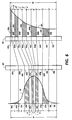
- FIG. 3 there is shown a typical beam with a Gaussian distribution 30 directed towards a facet of a rotating polygon mirror as in Figure 1.
- BDO binary diffraction optic
- the Gaussian distribution is divided into infinitesimal sections of equal energy bands 30a, 30b, 30c, 30d, 30e, 30f, 30g, 30h, 30i and 30j.
- Each one of the bands 30a, 30b, 30c, 30d, 30e, 30f, 30g, 30h, 30i and 30j has a width a, b, c, d, e, f, g, h, i and j respectively.
- the bands closer to the center of Gaussian distribution such as band 30e are narrower and have more intensity and the bands closer to the sides of the Gaussian distribution such as 30a are wider and have less intensity.
- the energy for all the bands is the same.
- the profile 50 which can have a width w equal to the width w of the Gaussian distribution 30, is divided into infinitesimal sections of equal energy bands 50a, 50b, 50c, 50d, 50e, 50f, 50g, 50h, 50i and 50j. Since the intensity of this profile 50 will be uniform, all bands 50a, 50b, 50c, 50d, 50e, 50f, 50g, 50h, 50i and 50h have equal widths n and contain the same energy.
- each one of the binary diffraction optic lenses 40 and 42 has to be designed to have a separate segment for each band. It should be noted that each segment has a plurality of infinitesimal stepped wedges (see Figures 4A and 4B).
- Each one of segments 40a, 40b, 40c, 40d, 40e, 40f, 40g, 40h, 40i and 40j is designed to convert the bands 30a, 30b, 30c, 30d, 30e, 30f, 30g, 30h, 30i and 30j into bands 50a, 50b, 50c, 50d, 50e, 50f, 50g, 50h, 50i and 50j respectively.
- each one of the segments 42a, 42b, 42c, 42d, 42e, 42f, 42g, 42h, 42i and 42j is designed to collimate each one of the bands 50a, 50b, 50c, 50d, 50e, 50f, 50g, 50h, 50i and 50j respectively.
- segment 40a of the BDO 40 has to be capable of receiving band 30a and converge it in such a manner that when the band 30a strikes a facet, it will have a narrower width n. Since the energy of each band is kept constant, the energy of band 50a will still be the same as band 30a. However, since the band 50a has a narrower width n and the energy is constant, the intensity increases. In other words, if a wide band of light is compressed into a narrower band the intensity of the narrower band increases.
- segment 40e of the BDO 40 has to be designed to be capable of receiving band 30e, diverging and, as needed, deflecting the band in such a manner that when it strikes a facet, it will have a wider width n. Since the width n is wider than width e and the energy is constant, the intensity decreases.
- Figure 4A shows a representative magnified exaggerated lower portion of segment 40a of Figure 3 and Figure 4B shows a representative magnified exaggerated upper portion of segment 40e of Figure 3.
- Figure 4A as the lower edge 37 of band 30a passes through the segment 40a and exits from one of the stepped wedges 41 of the segment 40a, it deflects.
- Figure 4B as the upper edge 39 of band 30e passes through the segment 40e and exits from one of the stepped wedges 43 of the segment 40e, it deflects.
- a uniform profile such as profile 50 improves the performance of an electro-optic modulator, which has a crystal 14.
- an electro-optic modulator crystal 14 has a beam profile 30 of uniform intensity, illuminating the active region of the modulator 14a, the electro-optic crystal is damaged uniformly in the active region 14a and due to the uniformity of the optical damage in the crystal, the index change is approximately uniform.
- the disclosed embodiment of this invention uses the light beam more efficiently since it allows utilization of a greater portion of the beam.
- Binary diffraction optic lenses are made using the same techniques used to fabricate VLSl circuits, as disclosed in Binary Optics Technology: The Theory and Design of Multi-level Diffractive Optical Elements by G.J. Swanson of the Lincoln Laboratory at the Massachusetts Institute of Technology, (Technical Report 854, 14 August 1989) and in US-A-4,895,790.
- a designer develops an idealized diffractive surface structure mathematically, then using a computer, defines a series of precise, microlithographic masks.
- a mask pattern is printed into a photoresist coating using a UV light source and then transferred into the optical substrate by ion milling or plasma etching.
- the BDO pair disclosed in the embodiment of this invention can be designed to reprofile any intensity profile of some given shape to any desirable intensity profile and can be used in any system which may need a certain intensity profile.
- Figures 6 and 7 illustrate the principal of this invention wherein two different intensity profiles are changed into desired profiles.
- Figure 6 changes the intensity profile 30 of Figure 3 to an intensity profile 64.
- Figure 7 changes an intensity profile 70 to an intensity profile 90.
- Figures 6 and 7 show only two of the unlimited possibilities of using this invention.
- the profile 64 which has a width w equal to the width w of the Gaussian distribution 30, has to be divided into infinitesimal sections of equal energy bands 64a, 64b, 64c, 64d, 64e, 64f, 64g, 64h, 64i and 64j.
- Each one of the bands 64a, 64b, 64c, 64d, 64e, 64f, 64g, 64h, 64i and 64j has a width a', b', c', d', e', f', g', h', i' and j' respectively.
- each one of the binary diffraction optic lenses 60 and 62 has to be designed to have a separate segment for each band.
- Each one of segments 60a, 60b, 60c, 60d, 60e, 60f, 60g, 60h, 60i and 60j is designed to convert the bands 30a, 30b, 30c, 30d, 30e, 30f, 30g, 30h, 30i and 30j into banos 64a, 64b, 64c, 64d, 64e, 64f, 64g, 64h, 64i and 64j respectively.
- each one of the segments 62a, 62b, 62c, 62d, 62e, 62f, 62g, 62h, 62i and 62j is designed to collimate each one of the bands 64a, 64b, 64c, 64d, 64e, 64f, 64g, 64h, 64i and 64j respectively.
- segment 60a of the BDO 60 has to be capable of receiving band 30a and converging it in such a manner that the band 30a will have a narrower width a' to achieve the intensity required. Since the band 30a has a narrower width a' at band 64a, the intensity increases. In other words, if a wide band of light is compressed into a narrower band the intensity of the narrower band increases.
- segment 60e of the BDO 60 has to be designed to be capable of receiving band 60e, diverging and deflecting, as needed, the band in such a manner that when it strikes a facet, it will have a wider width e' for the desired intensity decrease.
- a profile such as profile 64 is generated. It should be noted that depending on the desired profile, it might be necessary to have some segments of the BDO 60 to direct the bands through without diverging or converging the bands. Profile 64 has more intensity at one end and less intensity at the other end and a gradually decreasing intensity therebetween.
- each one of the binary diffraction optic lenses 80 and 82 has to be designed to have a separate segment for each band.
- Each one of segments 80a, 80b, 80c, 80d, 80e, 80f, 80g, 80h, 80i and 80j is designed to convert the bands 70a, 70b, 70c, 70d, 70e, 70f, 70g, 70h, 70i and 70j into bands 90a, 90b, 90c, 90d, 90e, 90f, 90g, 90h, 90i, and 90j respectively.
- each one of the segments 82a, 82b, 82c, 82d, 82e, 82f, 82g, 82h, 82i and 82j is designed to collimate each one of the bands 90a, 90b, 90c, 90d, 90e, 90f, 90g, 90h, 90i and 90j respectively.
Abstract
Description
- This invention relates to a raster scanner in which the intensity of a light beam is reprofiled across its width.
- Referring to Figure 1, a conventional raster scanner system utilizes a
light source 12, amodulator 14, a multi-faceted rotatingpolygon mirror 16 as the scanning element and aphotosensitive medium 18. Thelight source 12, which is typically a laser source, emits alight beam 20 and sends it to themodulator 14. Themodulator 14 receives pixel information and modulates thelight beam 20 in accordance with the pixel information. The raster scanner system utilizes overfill scanning and therefore, the modulatedlight beam 20 will be directed onto twofacets 22 of the rotatingpolygon mirror 16. The rotatingpolygon mirror 16 reflects thelight beam 20 and also causes thereflected light 20 to revolve about an axis near the center of rotation of the rotatingpolygon 16 and scans a line. Thisreflected light beam 20 can be utilized to impinge upon a photographic film or aphotosensitive medium 18, such as a xerographic drum at the output of the imaging system. - Referring to Figure 2, typically, a laser light beam has a
Gaussian distribution 30 which has a maximum intensity at the center C of the beam and a gradually decreasing intensity towards the outer shell S of the beam. In an overfilled raster scanner system in which a light beam is wide enough to cover at least two facets, an electro-optic crystal 14a used in themodulator 14 should be wide enough to encompass the width w of the light beam. However, since the intensity of the light beam varies from the center C of the beam to the outer shell 5, the surface of the electro-optic crystal 14a of themodulator 14 does not receive a uniform intensity. The center portion Ca of the electro-optic crystal is exposed to the maximum intensity from the center C of the light beam and the rest of the electro-optic crystal is exposed to less intensity. For example in lithium niobate crystal the non-uniform light excites carriers from impurities such as iron in the crystal. These carriers move in the crystal by diffusion and under the influence of electric fields are displaced to new positions and re-trapped, which results in specially varying refractive index changes due to the electro-optic effect. This phenomenon of index variation is called the "photorefractive effect" , or "optical damage" and is well documented in the literature. It is desirable in the case of information storage, but undesirable in the case of electro-optic modulator applications, since the index changes persist for long times and cause undesirable diffraction of light passing through the crystal. In particular the damage depends on the intensity of the light, which is not uniform in the case of a Gaussian beam. - Since the damage is greater near the center Ca of the electro-optic crystal, the performance of the center of the crystal degrades more than the performance of the rest of the crystal causing a non-uniform performance As damage occurs optical absorption increases accelerating the damage, further exacerbating the damage and a destructive cycle is set in motion. With a non-uniform performance, the performance of the center Ca of the crystal can drop to an unacceptable level while the performance of the rest of the crystal remains at the acceptable level. This effect is exaggerated when the intensity is sufficiently high that the outer areas can perform their proper function, resulting in excessive intensity near the crystal center leading to rapid deterioration. This problem can not be corrected by readjusting the
modulator 14. Readjustment of themodulator 14 can correct the performance of the center of the electro-optic crystal however, it over corrects the performance of the rest of the electro-optic crystal. Therefore, an electro-optic crystal, which is damaged only at the center, is no longer useful and it has to be replaced by a new electro-optic crystal. - It is an object of this invention to change the incident light beam intensity profile from a Gaussian distribution to a uniform intensity to the electro-optic crystal and thereby produce a nearly uniform damage in the region of the crystal, which performs optical modulation. Due to the difficulty of getting uniformity at the edges of the beam, the edges of the beam are designed to be outside the electro-optically modulated region of the modulator. The uniform intensity can be applied to other optical applications such as multi-channel AO modulators, or indeed any optical system application, which requires a uniform optical beam.
- It is a further object of this invention to change the intensity profile of a light beam from any intensity profile to any desired intensity profile.
- According to the present invention, there is provided an overfilled raster scanning apparatus comprising a light source emitting a light beam; a binary diffraction optic lens system comprising a first binary diffraction optic lens and a second binary diffraction optic lens spaced along said light beam path from said first binary diffraction optic lens; said binary diffraction optic lens system being arranged to receive said light beam from said light source and reprofile the intensity of said light beam across its width; a photo sensitive medium; and a rotating scanning means arranged to receive said reprofiled light beam from said binary diffraction optic lens system and scan said light beam across said photo sensitive medium.
- In one embodiment of the present invention, a pair of binary diffraction optic lenses are utilized to change the intensity profile of a light beam to a uniform intensity profile. For discussion purposes, both binary diffraction optic lenses of this invention can be considered divided into an equal number of segments. Each segment of the first binary diffraction optic lens either diverges or converges a portion of a light beam and, as needed, deflects the same portion of the beam. Each segment of the second binary diffraction optic lens receives the light beam from a respective segment of the first binary diffraction optic lens and collimates the light beam. In application, the segments are so small that the intensity profile change is essentially continuous.
- In another embodiment of the invention, a pair of binary diffraction optic lenses are utilized to change the intensity profile of a light beam from any profile to any desired profile. Both binary diffraction optic lenses of this invention have an equal number of segments. Depending on the shape of a desired intensity profile, each segment of the first binary diffraction optic lens either diverges or converges a portion of a light beam and, as needed, deflects the same portion of the beam. Each segment of the second binary diffraction optic lens receives the light beam from a respective segment of the first binary diffraction optic lens and collimates the light beam.
- A raster scanning apparatus in accordance with the invention will now be described, by way of example, with reference to the accompanying drawings, in which:-
- Figure 1 is a tangential view of a prior art raster output scanner;
- Figure 2 shows an electro-optic crystal of the modulator of Figure 1 exposed to a light beam with a Gaussian distribution;
- Figure 3 shows a Gaussian distribution reprofiled to a profile with a uniform intensity by a pair of binary diffraction optic lenses;
- Figure 4A is a representative magnified exaggerated lower portion of
segment 40a of Figure 3; - Figure 4B is a representative magnified exaggerated upper portion of
segment 40e of Figure 3; - Figure 5 shows an electro-optic crystal of a modulator exposed to a light beam with uniform intensity;
- Figure 6 shows a Gaussian distribution reprofiled by a pair of binary diffraction optic lenses to a profile with an intensity gradually decreasing from one end to the other end; and
- Figure 7 shows an arbitrary intensity profile reprofiled by a pair of binary diffraction optic lenses to another arbitrary profile.
- Referring to Figure 3, there is shown a typical beam with a
Gaussian distribution 30 directed towards a facet of a rotating polygon mirror as in Figure 1. In this invention, by using two binary diffraction optic (BDO)lenses profile 50 which has a uniform intensity profile. - To design binary diffraction
optic lenses equal energy bands bands band 30e are narrower and have more intensity and the bands closer to the sides of the Gaussian distribution such as 30a are wider and have less intensity. However, the energy for all the bands is the same. - Also, the
profile 50, which can have a width w equal to the width w of theGaussian distribution 30, is divided into infinitesimal sections ofequal energy bands profile 50 will be uniform, allbands - To convert the
Gaussian distribution 30 intoprofile 50, each one of the binary diffractionoptic lenses segments bands bands segments bands - For example,
segment 40a of the BDO 40 has to be capable of receivingband 30a and converge it in such a manner that when theband 30a strikes a facet, it will have a narrower width n. Since the energy of each band is kept constant, the energy ofband 50a will still be the same asband 30a. However, since theband 50a has a narrower width n and the energy is constant, the intensity increases. In other words, if a wide band of light is compressed into a narrower band the intensity of the narrower band increases. - On the contrary,
segment 40e of the BDO 40 has to be designed to be capable of receivingband 30e, diverging and, as needed, deflecting the band in such a manner that when it strikes a facet, it will have a wider width n. Since the width n is wider than width e and the energy is constant, the intensity decreases. - Figure 4A shows a representative magnified exaggerated lower portion of
segment 40a of Figure 3 and Figure 4B shows a representative magnified exaggerated upper portion ofsegment 40e of Figure 3. Referring to Figure 4A, as thelower edge 37 ofband 30a passes through thesegment 40a and exits from one of thestepped wedges 41 of thesegment 40a, it deflects. Also, referring to Figure 4B, as theupper edge 39 ofband 30e passes through thesegment 40e and exits from one of the steppedwedges 43 of thesegment 40e, it deflects. - Referring back to Figure 3, by converging the
bands segments BDO 40 and depending upon the intensity and the width of each band, by diverging or converging thebands segments profile 50 is generated. Since the width and the energy of each band is kept constant, the intensity of all the bands will also stay constant. Therefore, Theprofile 50 has a uniform intensity over the entire width of the light beam. - A uniform profile such as
profile 50 improves the performance of an electro-optic modulator, which has acrystal 14. Referring to Figure 5, when an electro-optic modulator crystal 14 has abeam profile 30 of uniform intensity, illuminating the active region of themodulator 14a, the electro-optic crystal is damaged uniformly in theactive region 14a and due to the uniformity of the optical damage in the crystal, the index change is approximately uniform. - In some optical applications such as raster scanner systems, only the center of the light beam can be used since the intensity of the rest of the beam is too low to be useful. The disclosed embodiment of this invention uses the light beam more efficiently since it allows utilization of a greater portion of the beam.
- Binary diffraction optic lenses are made using the same techniques used to fabricate VLSl circuits, as disclosed in Binary Optics Technology: The Theory and Design of Multi-level Diffractive Optical Elements by G.J. Swanson of the Lincoln Laboratory at the Massachusetts Institute of Technology, (
Technical Report 854, 14 August 1989) and in US-A-4,895,790. A designer develops an idealized diffractive surface structure mathematically, then using a computer, defines a series of precise, microlithographic masks. A mask pattern is printed into a photoresist coating using a UV light source and then transferred into the optical substrate by ion milling or plasma etching. - It should be noted that the BDO pair disclosed in the embodiment of this invention can be designed to reprofile any intensity profile of some given shape to any desirable intensity profile and can be used in any system which may need a certain intensity profile. Figures 6 and 7 illustrate the principal of this invention wherein two different intensity profiles are changed into desired profiles. Figure 6 changes the
intensity profile 30 of Figure 3 to anintensity profile 64. Figure 7 changes anintensity profile 70 to anintensity profile 90. Figures 6 and 7 show only two of the unlimited possibilities of using this invention. - Referring to Figure 6, the
profile 64, which has a width w equal to the width w of theGaussian distribution 30, has to be divided into infinitesimal sections ofequal energy bands bands - To convert the
Gaussian distribution 30 intoprofile 64, each one of the binarydiffraction optic lenses segments bands banos segments bands - For example,
segment 60a of theBDO 60 has to be capable of receivingband 30a and converging it in such a manner that theband 30a will have a narrower width a' to achieve the intensity required. Since theband 30a has a narrower width a' atband 64a, the intensity increases. In other words, if a wide band of light is compressed into a narrower band the intensity of the narrower band increases. - On the contrary,
segment 60e of theBDO 60 has to be designed to be capable of receivingband 60e, diverging and deflecting, as needed, the band in such a manner that when it strikes a facet, it will have a wider width e' for the desired intensity decrease. - By converging the
bands segments BDO 60 and depending upon the intensity and the width of each band by diverging or converging thebands segments profile 64 is generated. It should be noted that depending on the desired profile, it might be necessary to have some segments of theBDO 60 to direct the bands through without diverging or converging the bands.Profile 64 has more intensity at one end and less intensity at the other end and a gradually decreasing intensity therebetween. - Referring to Figure 7, to convert the given
distribution 70 into some desiredprofile 90, each one of the binarydiffraction optic lenses segments bands bands segments bands
Claims (4)
- An overfilled raster scanning apparatus comprising:
a light source emitting a light beam (30);
a binary diffraction optic lens system comprising a first binary diffraction optic lens (40) and a second binary diffraction optic lens (42) spaced along said light beam path from said first binary diffraction optic lens;
said binary diffraction optic lens system being arranged to receive said light beam from said light source and reprofile (50) the intensity of said light beam across its width (w);
a photo sensitive medium; and
a rotating scanning means arranged to receive said reprofiled light beam from said binary diffraction optic lens system and scan said light beam across said photo sensitive medium. - The raster scanning apparatus of claim 1, wherein said first binary diffraction optic lens (40) comprises a plurality of segments (40a-40j) at least some of which converge or diverge portions of said light beam and said second binary diffraction optic lens comprises a plurality of segments (42a-42j) which collimate said light beam.
- The raster scanning apparatus of claim 1 or claim 2, wherein segments (40a-40j) of said first binary diffraction optic lens which converge or diverge portions of said light beam respectively compress or expand said portions of said light beam so as to increase or decrease the intensity of said portions of said light beam.
- The raster scanning apparatus of claim 2 or claim 3 wherein said first binary diffraction optic lens comprises a plurality of segments arranged to converge and/or diverge at least some of said portions of the light beam such that said reprofiled light beam (50) is of substantially uniform intensity across its width.
Applications Claiming Priority (2)
| Application Number | Priority Date | Filing Date | Title |
|---|---|---|---|
| US990491 | 1992-12-14 | ||
| US07/990,491 US5315427A (en) | 1992-12-14 | 1992-12-14 | Pair of binary diffraction optics for use in overfilled raster output scanning systems |
Publications (2)
| Publication Number | Publication Date |
|---|---|
| EP0602872A2 true EP0602872A2 (en) | 1994-06-22 |
| EP0602872A3 EP0602872A3 (en) | 1995-05-10 |
Family
ID=25536209
Family Applications (1)
| Application Number | Title | Priority Date | Filing Date |
|---|---|---|---|
| EP93309795A Ceased EP0602872A3 (en) | 1992-12-14 | 1993-12-07 | Beam reprofiling by binary diffraction optics. |
Country Status (3)
| Country | Link |
|---|---|
| US (1) | US5315427A (en) |
| EP (1) | EP0602872A3 (en) |
| JP (1) | JPH06214184A (en) |
Cited By (2)
| Publication number | Priority date | Publication date | Assignee | Title |
|---|---|---|---|---|
| EP0967508A2 (en) * | 1998-06-23 | 1999-12-29 | Canon Kabushiki Kaisha | Scanning optical device |
| EP0848246B1 (en) * | 1996-12-11 | 2006-03-08 | G.D Societ Per Azioni | Method of measuring the intensity of radiation transmitted through a body |
Families Citing this family (25)
| Publication number | Priority date | Publication date | Assignee | Title |
|---|---|---|---|---|
| US5422753A (en) * | 1993-12-23 | 1995-06-06 | Xerox Corporation | Binary diffraction optical element for controlling scanning beam intensity in a raster output scanning (ROS) optical system |
| US5610733A (en) * | 1994-02-28 | 1997-03-11 | Digital Optics Corporation | Beam-homogenizer |
| US5850300A (en) | 1994-02-28 | 1998-12-15 | Digital Optics Corporation | Diffractive beam homogenizer having free-form fringes |
| US6392808B1 (en) | 1994-02-28 | 2002-05-21 | Digital Optics Corporation | Broad band controlled angle analog diffuser and associated methods |
| US5479583A (en) * | 1994-05-02 | 1995-12-26 | Xerox Corporation | Means to achieve a square intensity profile at an image plane by intensity and phase profiling |
| JP3104618B2 (en) * | 1996-05-10 | 2000-10-30 | 富士ゼロックス株式会社 | Optical scanning device and optical lens |
| US6008941A (en) * | 1996-06-25 | 1999-12-28 | Digital Optics Corporation | Optical soft aperture and use thereof |
| US5986807A (en) * | 1997-01-13 | 1999-11-16 | Xerox Corporation | Single binary optical element beam homogenizer |
| JPH11326804A (en) | 1998-03-16 | 1999-11-26 | Canon Inc | Color image forming device and scanning optical device |
| AUPP446598A0 (en) * | 1998-07-03 | 1998-07-30 | Australian National University, The | Planar lightwave circuits |
| US6542304B2 (en) | 1999-05-17 | 2003-04-01 | Toolz, Ltd. | Laser beam device with apertured reflective element |
| US6341030B1 (en) | 1999-07-14 | 2002-01-22 | Minolta Co., Ltd. | Light beam optical scanner and image forming apparatus |
| US6313948B1 (en) * | 1999-08-02 | 2001-11-06 | James I. Hanna | Optical beam shaper |
| DE102004035489A1 (en) * | 2004-07-19 | 2006-02-16 | Jenoptik Laser, Optik, Systeme Gmbh | Optical system for converting a primary intensity distribution into a given, space-angle-dependent intensity distribution |
| US7732166B2 (en) * | 2005-11-15 | 2010-06-08 | Oncohealth Corporation | Detection method for human pappilomavirus (HPV) and its application in cervical cancer |
| US7972776B2 (en) * | 2005-11-15 | 2011-07-05 | Oncohealth Corporation | Protein chips for HPV detection |
| US20070212859A1 (en) | 2006-03-08 | 2007-09-13 | Paul Carey | Method of thermal processing structures formed on a substrate |
| US7548364B2 (en) | 2006-07-31 | 2009-06-16 | Applied Materials, Inc. | Ultra-fast beam dithering with surface acoustic wave modulator |
| US20080025354A1 (en) * | 2006-07-31 | 2008-01-31 | Dean Jennings | Ultra-Fast Beam Dithering with Surface Acoustic Wave Modulator |
| US8916342B2 (en) | 2006-11-13 | 2014-12-23 | Oncohealth Corp. | Identification of high grade or ≧ CIN2 for early stages and late stages detection, screening, and diagnosis of human papillomavirus (HPV) and HPV-associated cancers |
| US8968995B2 (en) * | 2008-11-12 | 2015-03-03 | Oncohealth Corp. | Detection, screening, and diagnosis of HPV-associated cancers |
| US20100003704A1 (en) * | 2008-06-13 | 2010-01-07 | Shuling Cheng | IN SITU detection of early stages and late stages HPV infection |
| US8148663B2 (en) | 2007-07-31 | 2012-04-03 | Applied Materials, Inc. | Apparatus and method of improving beam shaping and beam homogenization |
| JP4943493B2 (en) * | 2009-12-04 | 2012-05-30 | シャープ株式会社 | Optical scanning apparatus and image forming apparatus having the same |
| US9128094B2 (en) | 2010-01-08 | 2015-09-08 | Oncohealth Corp. | High throughput cell-based HPV immunoassays for diagnosis and screening of HPV-associated cancers |
Citations (5)
| Publication number | Priority date | Publication date | Assignee | Title |
|---|---|---|---|---|
| US4895790A (en) * | 1987-09-21 | 1990-01-23 | Massachusetts Institute Of Technology | High-efficiency, multilevel, diffractive optical elements |
| US4941721A (en) * | 1989-06-01 | 1990-07-17 | Xerox Corporation | Raster scanning system utilizing overfilled polygon facet design |
| EP0395910A2 (en) * | 1989-04-29 | 1990-11-07 | Firma Carl Zeiss | Mirror for modification of the optical configuration of a light beam |
| WO1991016654A1 (en) * | 1990-04-13 | 1991-10-31 | Eastman Kodak Company | Hologon scanner with beam shaping stationary diffraction grating |
| EP0602870A2 (en) * | 1992-12-14 | 1994-06-22 | Xerox Corporation | Optimal filling of a polygon facet by beam reprofiling |
Family Cites Families (2)
| Publication number | Priority date | Publication date | Assignee | Title |
|---|---|---|---|---|
| US5208701A (en) * | 1991-12-24 | 1993-05-04 | Xerox Corporation | Wobble correction lens with binary diffractive optic surface and refractive cylindrical surface |
| US5258862A (en) * | 1992-12-10 | 1993-11-02 | Xerox Corporation | Rotating disc optical synchronization system using binary diffractive optical elements |
-
1992
- 1992-12-14 US US07/990,491 patent/US5315427A/en not_active Expired - Fee Related
-
1993
- 1993-11-18 JP JP5289114A patent/JPH06214184A/en active Pending
- 1993-12-07 EP EP93309795A patent/EP0602872A3/en not_active Ceased
Patent Citations (5)
| Publication number | Priority date | Publication date | Assignee | Title |
|---|---|---|---|---|
| US4895790A (en) * | 1987-09-21 | 1990-01-23 | Massachusetts Institute Of Technology | High-efficiency, multilevel, diffractive optical elements |
| EP0395910A2 (en) * | 1989-04-29 | 1990-11-07 | Firma Carl Zeiss | Mirror for modification of the optical configuration of a light beam |
| US4941721A (en) * | 1989-06-01 | 1990-07-17 | Xerox Corporation | Raster scanning system utilizing overfilled polygon facet design |
| WO1991016654A1 (en) * | 1990-04-13 | 1991-10-31 | Eastman Kodak Company | Hologon scanner with beam shaping stationary diffraction grating |
| EP0602870A2 (en) * | 1992-12-14 | 1994-06-22 | Xerox Corporation | Optimal filling of a polygon facet by beam reprofiling |
Non-Patent Citations (1)
| Title |
|---|
| HAN C.Y., ISHII Y., MURATA K.: 'Reshaping collimated laser beams with Gaussian profile to uniform profiles' APPLIED OPTICS vol. 22, no. 22, 15 November 1983, pages 3644 - 3647 * |
Cited By (3)
| Publication number | Priority date | Publication date | Assignee | Title |
|---|---|---|---|---|
| EP0848246B1 (en) * | 1996-12-11 | 2006-03-08 | G.D Societ Per Azioni | Method of measuring the intensity of radiation transmitted through a body |
| EP0967508A2 (en) * | 1998-06-23 | 1999-12-29 | Canon Kabushiki Kaisha | Scanning optical device |
| EP0967508A3 (en) * | 1998-06-23 | 2003-07-23 | Canon Kabushiki Kaisha | Scanning optical device |
Also Published As
| Publication number | Publication date |
|---|---|
| US5315427A (en) | 1994-05-24 |
| JPH06214184A (en) | 1994-08-05 |
| EP0602872A3 (en) | 1995-05-10 |
Similar Documents
| Publication | Publication Date | Title |
|---|---|---|
| US5315427A (en) | Pair of binary diffraction optics for use in overfilled raster output scanning systems | |
| EP0660153B1 (en) | Binary diffraction optical element for controlling scanning beam intensity in a raster output scanning (ROS) optical system | |
| US8068265B2 (en) | Scanning optical apparatus | |
| US6064417A (en) | Laser printer using multiple sets of lasers with multiple wavelengths | |
| US5331468A (en) | Intensity redistribution for exposure correction in an overfilled symmetrical laser printer | |
| US5111343A (en) | Gradient filter | |
| JPH07110451A (en) | Optical scanner | |
| US5455708A (en) | Passive scan angle doubling optical system | |
| EP0424786B1 (en) | Raster scanning system utilizing overfilled polygon facet design with non-reflective facet edges | |
| EP0526846A2 (en) | Plural-beam scanning optical apparatus | |
| JPH01210921A (en) | Xerographic printer capable of compensating tilt errors and scan curve errors | |
| EP0602870A2 (en) | Optimal filling of a polygon facet by beam reprofiling | |
| JP2781023B2 (en) | ROS type printing machine with vibration countermeasures | |
| JP2001215430A (en) | Scanning optical system and image forming device using the same | |
| US4527858A (en) | Uniform speed scanning lens having a high resolving power | |
| KR100404408B1 (en) | Optical scanning apparatus, multi-beam optical scanning apparatus and image-forming apparatus | |
| EP0575988A1 (en) | A symmetrical overfilled polygon laser scanner | |
| EP0577405A1 (en) | Scan uniformity correction | |
| EP0681394B1 (en) | Raster scanning apparatus with square intensity profile at an image plane | |
| US5969747A (en) | Efficient LED light geometry for optical printers | |
| JP2005017896A (en) | Optical scanner and image forming device using the same | |
| EP0695078B1 (en) | Fast scan spot correction in a polygon raster output scanner | |
| Owens et al. | Design Of A Compact Diode Laser Color Printer | |
| JPS6049296B2 (en) | scanning optical system | |
| JPH02217816A (en) | Light beam scanning device |
Legal Events
| Date | Code | Title | Description |
|---|---|---|---|
| PUAI | Public reference made under article 153(3) epc to a published international application that has entered the european phase |
Free format text: ORIGINAL CODE: 0009012 |
|
| AK | Designated contracting states |
Kind code of ref document: A2 Designated state(s): DE FR GB IT |
|
| PUAL | Search report despatched |
Free format text: ORIGINAL CODE: 0009013 |
|
| AK | Designated contracting states |
Kind code of ref document: A3 Designated state(s): DE FR GB IT |
|
| 17P | Request for examination filed |
Effective date: 19951110 |
|
| 17Q | First examination report despatched |
Effective date: 19980113 |
|
| STAA | Information on the status of an ep patent application or granted ep patent |
Free format text: STATUS: THE APPLICATION HAS BEEN REFUSED |
|
| 18R | Application refused |
Effective date: 20020917 |