EP0594464A2 - Method of operating a data storage disk array - Google Patents
Method of operating a data storage disk array Download PDFInfo
- Publication number
- EP0594464A2 EP0594464A2 EP93308454A EP93308454A EP0594464A2 EP 0594464 A2 EP0594464 A2 EP 0594464A2 EP 93308454 A EP93308454 A EP 93308454A EP 93308454 A EP93308454 A EP 93308454A EP 0594464 A2 EP0594464 A2 EP 0594464A2
- Authority
- EP
- European Patent Office
- Prior art keywords
- data
- parity
- drive
- old
- parity information
- Prior art date
- Legal status (The legal status is an assumption and is not a legal conclusion. Google has not performed a legal analysis and makes no representation as to the accuracy of the status listed.)
- Granted
Links
Images


Classifications
-
- G—PHYSICS
- G06—COMPUTING; CALCULATING OR COUNTING
- G06F—ELECTRIC DIGITAL DATA PROCESSING
- G06F11/00—Error detection; Error correction; Monitoring
- G06F11/07—Responding to the occurrence of a fault, e.g. fault tolerance
- G06F11/08—Error detection or correction by redundancy in data representation, e.g. by using checking codes
- G06F11/10—Adding special bits or symbols to the coded information, e.g. parity check, casting out 9's or 11's
- G06F11/1076—Parity data used in redundant arrays of independent storages, e.g. in RAID systems
-
- G—PHYSICS
- G06—COMPUTING; CALCULATING OR COUNTING
- G06F—ELECTRIC DIGITAL DATA PROCESSING
- G06F11/00—Error detection; Error correction; Monitoring
- G06F11/07—Responding to the occurrence of a fault, e.g. fault tolerance
- G06F11/08—Error detection or correction by redundancy in data representation, e.g. by using checking codes
- G06F11/10—Adding special bits or symbols to the coded information, e.g. parity check, casting out 9's or 11's
- G06F11/1008—Adding special bits or symbols to the coded information, e.g. parity check, casting out 9's or 11's in individual solid state devices
Landscapes
- Engineering & Computer Science (AREA)
- Theoretical Computer Science (AREA)
- Quality & Reliability (AREA)
- Physics & Mathematics (AREA)
- General Engineering & Computer Science (AREA)
- General Physics & Mathematics (AREA)
- Techniques For Improving Reliability Of Storages (AREA)
- Information Retrieval, Db Structures And Fs Structures Therefor (AREA)
- Detection And Correction Of Errors (AREA)
Abstract
Description
- This invention relates to a method of operating a data storage disk array.
- RAID (Redundant Array of Inexpensive Disks) storage systems have emerged as an alternative to large, expensive disk drives for use within present and future computer system architectures. A RAID storage system includes an array of small, inexpensive hard disk drives, such as the 5 1/4 or 3 1/2 inch disk drives currently used in personal computers and workstations. Although disk array products have been available for several years, significant improvements in the reliability and performance of small disk drives and a decline in the cost of such drives have resulted in the recent enhanced interest in RAID systems
- Current disk array design alternatives are described in an article titled "A Case for Redundant Arrays of Inexpensive Disks (RAID)" by David A. Patterson, Garth Gibson and Randy H. Katz; University of California Report No. UCB/CSD 87/391, December 1987. The article, discusses disk arrays and the improvements in performance, reliability, power consumption and scalability that disk arrays provide in comparison to single large magnetic disks. Five disk array arrangements, referred to as RAID levels, are described. The simplest array, a
RAID level 1 system comprises one or more disks for storing data and an equal number of additional "mirror" disks for storing copies of the information written to the data disks. The remaining RAID levels, identified asRAID level RAID level - A
RAID level 4 disk array is comprised of N+1 disks wherein N disks are used to store data, and the additional disk is utilized to store parity information. Data to be saved is divided into portions consisting of one or many blocks of data for storage among the disks. The corresponding parity information, which can be calculated by performing a bit-wise exclusive-OR of corresponding portions of the data stored across the N data drives, is written to the dedicated parity disk. The parity disk is used to reconstruct information in the event of a disk failure. Writes typically require access to two disks, i.e., one of the N data disks and the parity disk, as will be discussed in greater detail below. Read operations typically need only access a single one of the N data disks, unless the data to be read exceeds the block length stored on each disk. -
RAID level 5 disk arrays are similar toRAID level 4 systems except that parity information, in addition to the data, is distributed across the N+1 disks in each group. Each one of the N+1 disks within the array includes some blocks for storing data and some blocks for storing parity information. Where parity information is stored is controlled by an algorithm implemented by the user. As inRAID level 4 systems,RAID level 5 writes typically require access to two disks; however, no longer does every write to the array require access to the same dedicated parity disk, as inRAID level 4 systems. This feature provides the opportunity to perform concurrent write operations. - A
RAID level 5 system including five data and parity disk drives, DRIVE A through DRIVE E, and a spare disk drive, DRIVE F, is illustrated in Figure 1. Anarray controller 100 coordinates the transfer of data between thehost system 147 and the array disk drives. The controller also calculates and checks parity information.Blocks 145A through 145E illustrate the manner in which data and parity is stored on the five array drives. Data blocks are identified asBLOCK 0 throughBLOCK 15. Parity blocks are identified as PARITY 0 through PARITY 3. The relationship between the parity and data blocks is as follows:PARITY 0 = (BLOCK 0) XOR (BLOCK 1) XOR (BLOCK 2) XOR (BLOCK 3) -
PARITY 1 = (BLOCK 4) XOR (BLOCK 5) XOR (BLOCK 6) XOR (BLOCK 7) - PARITY 2 = (BLOCK 8) XOR (BLOCK 9) XOR (BLOCK 10) XOR (BLOCK 11)
- PARITY 3 = (BLOCK 12) XOR (BLOCK 13) XOR (BLOCK 14) XOR (BLOCK 15)
- As stated above, parity data can be calculated by performing a bit-wise exclusive-OR of corresponding portions of the data stored across the N data drives. However, because each parity bit is simply the exclusive-OR product of all the corresponding data bits from the data drives, new parity can be more easily determined from the old data and the old parity as well as the new data in accordance with the following equation:
- new parity (old data XOR new data) XOR old parity.
- Although the parity calculation for
RAID levels typical RAID level RAID level RAID level - It is an object of the present invention to provide a method of efficiently operating a data storage disk array.
- Therefore, according to the present invention there is provided a method of operating a data storage disk array including first and second disk drives in response to the receipt of new data from a host system, characterized by the steps of: reading old data from said first drive and saving said old data to a first storage buffer; writing said new data to a second storage buffer; replacing said old data residing on said first drive with said new data; generating new parity information after the conclusion of said reading step; and replacing said old parity information residing on said second drive with said new parity information.
- One embodiment of the present invention will now be described by way of example, with reference to the accompanying drawings, in which:-
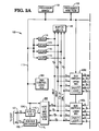
- Figure 1 is a block diagram representation of a
RAID level 5 array including six disk drives. - Figures 2Aand 2B illustrate in block diagram form one possible architecture for
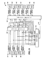
disk array controller 100 shown in Figure 1. - Figure 3 is a block diagram illustration of the logic included within
Bus Switch block 400U shown in Figures 2A and 2B. - Figures 4 and 5 illustrate a
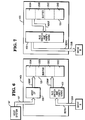
RAID level 5 read-modify-write operation. - Figures 6 through 9 illustrate the modified
RAID level 5 write operation wherein parity write operations are delayed in accordance with the method of the present invention. - Referring now to Figures 2Aand 2B, the architecture of a
disk array controller 100 for a RAID system is shown in block diagram form. The array controller coordinates the operation of the multitude of disk drives within the array to perform read and write functions, parity generation and checking, and data restoration and reconstruction. The controller exchanges data with the host computer system (not shown) through Host Interface andCRC Logic block 200. Host I/F Logic block 200, under the control ofprocessor 101, interfaces an external 18-bit or 36-bit wide, SCSI-2bus 107 associated with the host system with four internal 18-bit wide buffer busses ABUF, BBUF, CBUF and DBUF.Bus 107 connects to Host I/F Logic block 200 through a standard SCSI-2 chip set, represented byblocks bit busses block 200 andprocessor 101 is provided by address/data bus 113. - Host I/F Logic Block 200 operates to multiplex data between SCSI-2
devices Block 200 provides multiplexing functionality betweenbusses RAID level 3 and highbandwidth RAID level 5 applications by word striping data across the four buffer busses in a rotating sequential order, (2) one of two defined pairs of buffer busses for 2 + 1RAID level 3 applications by word striping data across the pair of buffer busses in a rotating sequential order, of (3) any one of the buffer busses forRAID level 1 and singlebus RAID level 5 applications. - Internal buffer busses ABUF, BBUF, CBUF and DBUF connect Host I/
F Logic block 200 with aRAM buffer 120 and upper and lowerbyte bus switches Buffer 120 possesses the capability to read and write 72-bit wide words from the four buffer busses, or individual 18-bit wide words from any one of the buffer busses. Eighteen or 36-bit access is also provided throughtransceivers 115 tobus 113. -
Bus switches Bus switches bus switches - Each one of drive busses ADRV, BDRV, CDRV, DDRV, EDRV and FDRV is connected to an associated SCSI-2 device, labeled 130A through 130F, which provide connection to six corresponding disk drives (not shown) forming the disk array. The six drives will be identified herein as drives A through F. Reed-Solomon Cyclic Redundancy Check (RSCRC) logic blocks 500AB, 500CD and 500EF are connected between busses ADRV and BDRV, CDRV and DDRV, and EDRV and FDRV, respectively, to provide error detection and generation of Reed-Solomon CRC for the array controller.
- The control of Host I/
F Logic block 200;bus switches SCSI devices microprocessor 101. Communication betweenmicroprocessor 101, associatedprocessor memory 103 andprocessor control inputs 105 and the above-identified elements is provided by address/data bus 113. Also shown connected tobus 113 is DMAControl Logic block 300. The logic withinblock 300 provides DMA control for Host I/F Logic block 200, bus switches 400 U and 400L, SCSI-2devices 130A through 130F andprocessor 101. - The controller architecture shown in Figures 2A and 2B can be configured to accommodate different quantities of disk drives and also to accommodate different RAID configurations.
- The logic included within each one of
bus switches reference numerals 491 through 496, connect with the six disk drive busses ADRV, BDRV, CDRV, DDRV, EDRV and FDRV, respectively. Bus switches 400U and 400L operate together to provide a unidirectional connection between any one of controller buses ABUF, BBUF, CBUF and DBUF and any one of drive buses ADRV, BDRV, CDRV, DDRV, EDRV and FDRV. Multiple connections between several controller busses and an equal number of drive busses is also permitted. Additionally, the bus switches may provide unidirectional connection of any controller bus to two or more drive busses. Parity information obtained viabus 453 can also be ported to any one of the drive busses. - The architecture of each bus switch is composed of three primary blocks: a
latch module 450,switch module 460, and aparity module 470.Switch module 460 is connected between controller busses ABUF, BBUF, CBUF and DBUF and drive busses ADRV, BDRV, CDRV, DDRV, EDRV and FDRV. Anadditional bus 453 connectsparity module 470 tobus switch module 460. Several functions are provided bybus switch module 460. First,bus switch module 460 provides a unidirectional connection between any controller bus and any drive bus. Multiple connections between several controller busses and an equal number of drive busses is also permitted. - Second, the bus switch module provides connection between any two or more of the drive busses. Such an operation is necessary for the transfer of information between disk drives without interfering with host or controller operations.
- Third,
bus switch module 460 provides connection between any two or more of the controller busses. This mode of operation supports data reorganization on the controller by allowing data to be propagated from one controller bus to another. This mode of turnaround operation is also advantageous for BIST (Built-In Self Test) development. - Finally, the bus switch module provides unidirectional connection of any controller bus to one or more drive busses. Parity information obtained via
bus 453 can also be ported to any one of the drive busses. -
Parity module 470 includes connections to each of the controller busses for receiving data therefrom and a connection tobus 453 for providing parity information tobus switch module 460.Parity module 470 generates parity information forRAID level bus switch module 460 viabus 453. - Figures 4 and 5 illustrate a
RAID level 5 write involving DRIVE A and DRIVE B, wherein data is to be written to DRIVE B and parity information is to be updated on DRIVE A. Only structure required to facilitate the read-modify-write (RMW) operation is shown in Figures 4 and 5. - Under direction of the controller processor, not shown, old data and parity information are first read from the two drives as shown in Figure 4. The old data and parity are read from the target areas within drives DRIVE B and DRIVE A, respectively, and routed via
buses bus switch 400.Bus switch 400 is configured to combine the received data and parity to generate the exclusive-OR product: - old data XOR old parity. This product is stored in a
first area 120D withinbuffer 120. New data received fromhost system 147 is concurrently saved to a secondarea 120Awithin buffer 120. - New data and parity information is then written to DRIVE B and DRIVE A as shown in Figure 5.
Bus switch 400 is reconfigured to route the new data read fromarea 120A instorage buffer 120 to DRIVEB. Bus switch 400 is further configured to generate new parity information by combining the new data with the previously saved product, old data XOR old parity, stored instorage buffer area 120D. The result, old data XOR old parity XOR new data, is written to DRIVE A. - Figures 6 through 9 illustrate the modified
RAID level 5 write operation wherein parity write operations are delayed in accordance with the method of the present invention. As with Figure 4 and 5, only structure required to facilitate the write operation is shown in Figures 6 through 9. - Figure 6 illustrates the first step in the modified
RAID level 5 write operation. During this first step old data received from disk storage and new data received from the host system is saved to buffer 120. In Figure 6, the new data received fromhost system 147 is directed through host I/F logic 200 and buffer bus ABUF to a first storage area withinbuffer 120. Old data is read from DRIVE B and routed viadrive buses 135B and BDRV,bus switch 400 and buffer bus DBUF to a second storage area withinbuffer 120. The new data received fromhost system 147 is directed through host I/F logic 200 and buffer bus ABUF to a second storage area withinbuffer 120.Bus switch 400 is thereafter reconfigured and the new data stored inbuffer 120 is written to DRIVE B as shown in Figure 7. - Old parity is read from Drive A and written to
area 120D withinbuffer 120 as shown in Figure 8. This step may be performed concurrendy with, or at any point after, the operation shown in Figure 6 wherein old data is read from DRIVE B and saved tostorage buffer 120.Bus switch 400 is thereafter configured to generate new parity information by combining the new data fromstorage area 120A, old data fromstorage area 120C and the old parity fromstorage area 120D as shown in Figure 9. The result, old data XOR old parity XOR new data, is written to DRIVE A. The new parity write operation shown in Figure 9 may be performed immediately upon the conclusion of the old parity read operation shown in Figure 8, or may be delayed for execution at a more suitable time. - Separating the DRIVE B (data) and DRIVE A (parity) read and write operations allows for more efficient utilization of the disk drives. In the RMW procedure shown in Figures 4 and 5 and discussed above, a delay in obtaining access to either the parity or data drives delays the entire RMW operation. Data on DRIVE B is updated as soon as the drive is available; the update is not delayed in the event the parity drive, DRIVE A, is unavailable. Similarly, DRIVE Aop- erations will not be stayed should DRIVE B be unavailable.
- By delaying the parity read and write operations involving DRIVE A, the method of the present invention permits utilization of DRIVE A for other input/out- put operations until such time as the parity read, generate and write operations (Figures 8 and 9) can proceed efficiently without inducing disk service time penalties.
- Scheduling of disk read and write operations is coordinated by the array controller which maintains separate I/O queues for each drive within the array. The method identifies the disk drives containing the data and parity to be updated, drives. DRIVE B and DRIVE A in the example described above, and places the proper read and write requests into the I/O queues for the identified data and parity drives, scheduling parity operations; i.e. reading old parity information from DRIVE A, generating new parity information and writing the new parity information to DRIVE A; for execution when best accommodated in the I/O queue for DRIVE A, following the read of old data from DRIVE B.
- In addition, in order to minimize the overall response time seen by the host system upon issuing a write request, the modified write routine may include procedures for reporting write completion status to the host system just after the write of data to DRIVE B is completed, without waiting for the associated parity generation and write to DRIVE A to complete.
- To assure data reliability and integrity of parity in the array in the event of an array or drive failure, the array controller maintains a status table which identifies the pending parity blocks. Moreover, this status table should be placed in a safe secondary storage device, apart from the array controller, so as to survive a controller failure and allow recovery.
- It can thus be seen that there has been provided by the present invention a method which improves the efficiency of disk drive utilization within a disk array, minimizing I/O service times and I/O queue waiting times for individual drives within the diskarray. Although a
RAID level 5 system including an array controller and five disk drives for the storage of data and parity information is shown in the Figures, and discussed above, those skilled in the art will recognize that the invention is not limited to the specific embodiment described above and that numerous modifications and changes are possible without departing from the scope of the present invention. For example, the method may be utilized to improve the performance ofRAID level 4 and other disk array systems. The method may also be employed by the host system processor for those disk array systems not including a dedicated array controller.
Claims (4)
Applications Claiming Priority (2)
| Application Number | Priority Date | Filing Date | Title |
|---|---|---|---|
| US966106 | 1992-10-23 | ||
| US07/966,106 US5388108A (en) | 1992-10-23 | 1992-10-23 | Delayed initiation of read-modify-write parity operations in a raid level 5 disk array |
Publications (3)
| Publication Number | Publication Date |
|---|---|
| EP0594464A2 true EP0594464A2 (en) | 1994-04-27 |
| EP0594464A3 EP0594464A3 (en) | 1998-02-11 |
| EP0594464B1 EP0594464B1 (en) | 2001-12-19 |
Family
ID=25510924
Family Applications (1)
| Application Number | Title | Priority Date | Filing Date |
|---|---|---|---|
| EP93308454A Expired - Lifetime EP0594464B1 (en) | 1992-10-23 | 1993-10-22 | Method of operating a data storage disk array |
Country Status (4)
| Country | Link |
|---|---|
| US (1) | US5388108A (en) |
| EP (1) | EP0594464B1 (en) |
| JP (1) | JPH0772985A (en) |
| DE (1) | DE69331369T2 (en) |
Cited By (11)
| Publication number | Priority date | Publication date | Assignee | Title |
|---|---|---|---|---|
| EP0718766A2 (en) * | 1994-12-21 | 1996-06-26 | Symbios Logic Inc. | Method of operating a disk drive array |
| US5964895A (en) * | 1996-12-05 | 1999-10-12 | Electronics And Telecommunications Research Institute | VRAM-based parity engine for use in disk array controller |
| EP1486871A2 (en) * | 1996-11-21 | 2004-12-15 | Hitachi, Ltd. | Disk array device and method for controlling the same |
| US8103903B2 (en) | 2010-02-22 | 2012-01-24 | International Business Machines Corporation | Read-modify-write protocol for maintaining parity coherency in a write-back distributed redundancy data storage system |
| US8103904B2 (en) | 2010-02-22 | 2012-01-24 | International Business Machines Corporation | Read-other protocol for maintaining parity coherency in a write-back distributed redundancy data storage system |
| US8156368B2 (en) | 2010-02-22 | 2012-04-10 | International Business Machines Corporation | Rebuilding lost data in a distributed redundancy data storage system |
| US8578094B2 (en) | 2010-02-22 | 2013-11-05 | International Business Machines Corporation | Full-stripe-write protocol for maintaining parity coherency in a write-back distributed redundancy data storage system |
| CN103902232A (en) * | 2012-12-28 | 2014-07-02 | 联想(北京)有限公司 | Data write-in method and device |
| CN106339179A (en) * | 2015-07-06 | 2017-01-18 | 上海宝存信息科技有限公司 | Host Device, Access System, and Access Method |
| US10127233B2 (en) | 2013-12-31 | 2018-11-13 | Huawei Technologies Co., Ltd. | Data processing method and device in distributed file storage system |
| US10191841B2 (en) | 2015-07-06 | 2019-01-29 | Shannon Systems Ltd. | Host device, access system, and access method |
Families Citing this family (38)
| Publication number | Priority date | Publication date | Assignee | Title |
|---|---|---|---|---|
| JPH06332623A (en) * | 1993-05-24 | 1994-12-02 | Mitsubishi Electric Corp | Array type recorder and recorder |
| GB2289779B (en) * | 1994-05-24 | 1999-04-28 | Intel Corp | Method and apparatus for automatically scrubbing ECC errors in memory via hardware |
| JPH0830397A (en) * | 1994-07-20 | 1996-02-02 | Sony Corp | Information storage device |
| JP3661205B2 (en) * | 1994-09-09 | 2005-06-15 | 株式会社日立製作所 | Disk array system and method for generating parity data of disk array system |
| US5671439A (en) * | 1995-01-10 | 1997-09-23 | Micron Electronics, Inc. | Multi-drive virtual mass storage device and method of operating same |
| US5745671A (en) * | 1995-02-28 | 1998-04-28 | International Business Machines Corporation | Data storage system with localized XOR function |
| US5737744A (en) * | 1995-10-13 | 1998-04-07 | Compaq Computer Corporation | Disk array controller for performing exclusive or operations |
| US5860090A (en) * | 1995-10-20 | 1999-01-12 | Informix Software, Inc. | Append-only storage in a disk array using striping and parity caching |
| US5778426A (en) * | 1995-10-23 | 1998-07-07 | Symbios, Inc. | Methods and structure to maintain a two level cache in a RAID controller and thereby selecting a preferred posting method |
| US5720025A (en) * | 1996-01-18 | 1998-02-17 | Hewlett-Packard Company | Frequently-redundant array of independent disks |
| KR100275900B1 (en) * | 1996-09-21 | 2000-12-15 | 윤종용 | Method for implement divideo parity spare disk in raid sub-system |
| US5883909A (en) * | 1996-11-06 | 1999-03-16 | Lsi Logic Corporation | Method and apparatus for reducing data transfers across a memory bus of a disk array controller |
| US5835694A (en) * | 1996-12-06 | 1998-11-10 | International Business Machines Corporation | Raid-configured disk drive array wherein array control occurs at the disk drive level |
| US6073218A (en) * | 1996-12-23 | 2000-06-06 | Lsi Logic Corp. | Methods and apparatus for coordinating shared multiple raid controller access to common storage devices |
| US5933824A (en) * | 1996-12-23 | 1999-08-03 | Lsi Logic Corporation | Methods and apparatus for locking files within a clustered storage environment |
| US5944838A (en) * | 1997-03-31 | 1999-08-31 | Lsi Logic Corporation | Method for fast queue restart after redundant I/O path failover |
| US5953352A (en) * | 1997-06-23 | 1999-09-14 | Micron Electronics, Inc. | Method of checking data integrity for a raid 1 system |
| US6061822A (en) * | 1997-06-23 | 2000-05-09 | Micron Electronics, Inc. | System and method for providing a fast and efficient comparison of cyclic redundancy check (CRC/checks sum) values of two mirrored disks |
| US6098114A (en) * | 1997-11-14 | 2000-08-01 | 3Ware | Disk array system for processing and tracking the completion of I/O requests |
| US5987628A (en) * | 1997-11-26 | 1999-11-16 | Intel Corporation | Method and apparatus for automatically correcting errors detected in a memory subsystem |
| US6035347A (en) * | 1997-12-19 | 2000-03-07 | International Business Machines Corporation | Secure store implementation on common platform storage subsystem (CPSS) by storing write data in non-volatile buffer |
| JPH11203056A (en) | 1998-01-19 | 1999-07-30 | Fujitsu Ltd | Input/output controller and array disk device |
| US6223323B1 (en) * | 1998-07-17 | 2001-04-24 | Ncr Corporation | Method for storing parity information in a disk array storage system |
| US6343343B1 (en) | 1998-07-31 | 2002-01-29 | International Business Machines Corporation | Disk arrays using non-standard sector sizes |
| US6405284B1 (en) | 1998-10-23 | 2002-06-11 | Oracle Corporation | Distributing data across multiple data storage devices in a data storage system |
| US6530035B1 (en) | 1998-10-23 | 2003-03-04 | Oracle Corporation | Method and system for managing storage systems containing redundancy data |
| US6330625B1 (en) * | 1999-01-15 | 2001-12-11 | Oracle Corporation | System for initiating multiple read operation requests to multiple copies of a data item and identifying a first one of the requests as having the fastest response time |
| US6425055B1 (en) | 1999-02-24 | 2002-07-23 | Intel Corporation | Way-predicting cache memory |
| US6418512B1 (en) | 1999-08-31 | 2002-07-09 | International Business Machines Corporation | Method and system for reporting disk utilizations for disk subsystems |
| US7127668B2 (en) * | 2000-06-15 | 2006-10-24 | Datadirect Networks, Inc. | Data management architecture |
| US20060259683A1 (en) * | 2005-05-16 | 2006-11-16 | Oracle International Corporation | Method and system for disk stippling |
| CN100397352C (en) * | 2005-09-15 | 2008-06-25 | 威盛电子股份有限公司 | Return circuit for detecting magnetic disk array and method thereof |
| US7680992B1 (en) * | 2006-06-14 | 2010-03-16 | Nvidia Corporation | Read-modify-write memory with low latency for critical requests |
| US8296337B2 (en) | 2006-12-06 | 2012-10-23 | Fusion-Io, Inc. | Apparatus, system, and method for managing data from a requesting device with an empty data token directive |
| US8458515B1 (en) * | 2009-11-16 | 2013-06-04 | Symantec Corporation | Raid5 recovery in a high availability object based file system |
| US8478938B2 (en) | 2010-10-28 | 2013-07-02 | Lsi Corporation | Performing data writes in parity protected redundant storage arrays |
| WO2016051512A1 (en) * | 2014-09-30 | 2016-04-07 | 株式会社日立製作所 | Distributed storage system |
| US20180113616A1 (en) * | 2016-10-21 | 2018-04-26 | Nec Corporation | Disk array control device, disk array device, disk array control method, and recording medium |
Family Cites Families (4)
| Publication number | Priority date | Publication date | Assignee | Title |
|---|---|---|---|---|
| US4884271A (en) * | 1987-12-28 | 1989-11-28 | International Business Machines Corporation | Error checking and correcting for read-modified-write operations |
| US4914656A (en) * | 1988-06-28 | 1990-04-03 | Storage Technology Corporation | Disk drive memory |
| US5265098A (en) * | 1990-08-03 | 1993-11-23 | International Business Machines Corporation | Method and means for managing DASD array accesses when operating in degraded mode |
| US5257362A (en) * | 1991-03-08 | 1993-10-26 | International Business Machines Corporation | Method and means for ensuring single pass small read/write access to variable length records stored on selected DASDs in a DASD array |
-
1992
- 1992-10-23 US US07/966,106 patent/US5388108A/en not_active Expired - Lifetime
-
1993
- 1993-10-22 DE DE69331369T patent/DE69331369T2/en not_active Expired - Fee Related
- 1993-10-22 EP EP93308454A patent/EP0594464B1/en not_active Expired - Lifetime
- 1993-10-22 JP JP5286277A patent/JPH0772985A/en active Pending
Non-Patent Citations (2)
| Title |
|---|
| "METHOD FOR BACKGROUND PARITY UPDATE IN A REDUNDANT ARRAY OR INEXPENSIVE DISK (RAID)" IBM TECHNICAL DISCLOSURE BULLETIN, vol. 35, no. 5, October 1992, USA, pages 139-141, XP000312912 * |
| "Performance Assist for Checksum DASD" IBM TECHNICAL DISCLOSURE BULLETIN, vol. 32, no. 7, December 1989, USA, pages 5-7, XP000077997 * |
Cited By (16)
| Publication number | Priority date | Publication date | Assignee | Title |
|---|---|---|---|---|
| EP0718766A2 (en) * | 1994-12-21 | 1996-06-26 | Symbios Logic Inc. | Method of operating a disk drive array |
| EP0718766A3 (en) * | 1994-12-21 | 1999-03-17 | Hyundai Electronics America | Method of operating a disk drive array |
| EP1486871A2 (en) * | 1996-11-21 | 2004-12-15 | Hitachi, Ltd. | Disk array device and method for controlling the same |
| EP1486871A3 (en) * | 1996-11-21 | 2005-01-05 | Hitachi, Ltd. | Disk array device and method for controlling the same |
| US6961816B2 (en) | 1996-11-21 | 2005-11-01 | Hitachi, Ltd. | Disk array device with selectable method for generating redundant data |
| US5964895A (en) * | 1996-12-05 | 1999-10-12 | Electronics And Telecommunications Research Institute | VRAM-based parity engine for use in disk array controller |
| US8156368B2 (en) | 2010-02-22 | 2012-04-10 | International Business Machines Corporation | Rebuilding lost data in a distributed redundancy data storage system |
| US8103904B2 (en) | 2010-02-22 | 2012-01-24 | International Business Machines Corporation | Read-other protocol for maintaining parity coherency in a write-back distributed redundancy data storage system |
| US8103903B2 (en) | 2010-02-22 | 2012-01-24 | International Business Machines Corporation | Read-modify-write protocol for maintaining parity coherency in a write-back distributed redundancy data storage system |
| US8578094B2 (en) | 2010-02-22 | 2013-11-05 | International Business Machines Corporation | Full-stripe-write protocol for maintaining parity coherency in a write-back distributed redundancy data storage system |
| US8583866B2 (en) | 2010-02-22 | 2013-11-12 | International Business Machines Corporation | Full-stripe-write protocol for maintaining parity coherency in a write-back distributed redundancy data storage system |
| CN103902232A (en) * | 2012-12-28 | 2014-07-02 | 联想(北京)有限公司 | Data write-in method and device |
| CN103902232B (en) * | 2012-12-28 | 2018-11-09 | 联想(北京)有限公司 | A kind of method and device of the data of write-in |
| US10127233B2 (en) | 2013-12-31 | 2018-11-13 | Huawei Technologies Co., Ltd. | Data processing method and device in distributed file storage system |
| CN106339179A (en) * | 2015-07-06 | 2017-01-18 | 上海宝存信息科技有限公司 | Host Device, Access System, and Access Method |
| US10191841B2 (en) | 2015-07-06 | 2019-01-29 | Shannon Systems Ltd. | Host device, access system, and access method |
Also Published As
| Publication number | Publication date |
|---|---|
| DE69331369T2 (en) | 2002-06-20 |
| EP0594464B1 (en) | 2001-12-19 |
| DE69331369D1 (en) | 2002-01-31 |
| EP0594464A3 (en) | 1998-02-11 |
| JPH0772985A (en) | 1995-03-17 |
| US5388108A (en) | 1995-02-07 |
Similar Documents
| Publication | Publication Date | Title |
|---|---|---|
| EP0594464B1 (en) | Method of operating a data storage disk array | |
| US5596708A (en) | Method and apparatus for the protection of write data in a disk array | |
| US5418925A (en) | Fast write I/O handling in a disk array using spare drive for buffering | |
| US5487160A (en) | Concurrent image backup for disk storage system | |
| US5345565A (en) | Multiple configuration data path architecture for a disk array controller | |
| US5533190A (en) | Method for maintaining parity-data consistency in a disk array | |
| US5077736A (en) | Disk drive memory | |
| US5566316A (en) | Method and apparatus for hierarchical management of data storage elements in an array storage device | |
| US4989205A (en) | Disk drive memory | |
| EP0572564B1 (en) | Parity calculation in an efficient array of mass storage devices | |
| US4989206A (en) | Disk drive memory | |
| US4914656A (en) | Disk drive memory | |
| US5146588A (en) | Redundancy accumulator for disk drive array memory | |
| JP3237736B2 (en) | Matrix structure of data storage device | |
| JP3041214B2 (en) | Fault-tolerant data storage subsystem and data processing system | |
| US5720027A (en) | Redundant disc computer having targeted data broadcast | |
| US5727144A (en) | Failure prediction for disk arrays | |
| JP3742494B2 (en) | Mass storage device | |
| US5872906A (en) | Method and apparatus for taking countermeasure for failure of disk array | |
| GB2271462A (en) | Disk array recording system | |
| JPH08328760A (en) | Disk array device | |
| US6223323B1 (en) | Method for storing parity information in a disk array storage system | |
| US6023754A (en) | Multiple channel data bus routing switching including parity generation capabilities | |
| US5787463A (en) | Disk array system including a dual-ported staging memory and concurrent redundancy calculation capability | |
| JP3263647B2 (en) | Magnetic disk device and information transfer method |
Legal Events
| Date | Code | Title | Description |
|---|---|---|---|
| PUAI | Public reference made under article 153(3) epc to a published international application that has entered the european phase |
Free format text: ORIGINAL CODE: 0009012 |
|
| AK | Designated contracting states |
Kind code of ref document: A2 Designated state(s): DE FR GB |
|
| RAP1 | Party data changed (applicant data changed or rights of an application transferred) |
Owner name: AT&T GLOBAL INFORMATION SOLUTIONS INTERNATIONAL IN |
|
| RAP1 | Party data changed (applicant data changed or rights of an application transferred) |
Owner name: HYUNDAI ELECTRONICS AMERICA Owner name: AT&T GLOBAL INFORMATION SOLUTIONS INTERNATIONAL IN |
|
| RAP1 | Party data changed (applicant data changed or rights of an application transferred) |
Owner name: SYMBIOS LOGIC INC. Owner name: HYUNDAI ELECTRONICS AMERICA Owner name: AT&T GLOBAL INFORMATION SOLUTIONS INTERNATIONAL IN |
|
| RAP1 | Party data changed (applicant data changed or rights of an application transferred) |
Owner name: SYMBIOS LOGIC INC. Owner name: HYUNDAI ELECTRONICS AMERICA Owner name: NCR INTERNATIONAL, INC. |
|
| PUAL | Search report despatched |
Free format text: ORIGINAL CODE: 0009013 |
|
| AK | Designated contracting states |
Kind code of ref document: A3 Designated state(s): DE FR GB |
|
| RAP1 | Party data changed (applicant data changed or rights of an application transferred) |
Owner name: SYMBIOS, INC. Owner name: HYUNDAI ELECTRONICS AMERICA Owner name: NCR INTERNATIONAL, INC. |
|
| 17P | Request for examination filed |
Effective date: 19980730 |
|
| 17Q | First examination report despatched |
Effective date: 19991130 |
|
| GRAG | Despatch of communication of intention to grant |
Free format text: ORIGINAL CODE: EPIDOS AGRA |
|
| GRAG | Despatch of communication of intention to grant |
Free format text: ORIGINAL CODE: EPIDOS AGRA |
|
| GRAH | Despatch of communication of intention to grant a patent |
Free format text: ORIGINAL CODE: EPIDOS IGRA |
|
| GRAH | Despatch of communication of intention to grant a patent |
Free format text: ORIGINAL CODE: EPIDOS IGRA |
|
| GRAA | (expected) grant |
Free format text: ORIGINAL CODE: 0009210 |
|
| AK | Designated contracting states |
Kind code of ref document: B1 Designated state(s): DE FR GB |
|
| REG | Reference to a national code |
Ref country code: GB Ref legal event code: IF02 |
|
| REF | Corresponds to: |
Ref document number: 69331369 Country of ref document: DE Date of ref document: 20020131 |
|
| PLBE | No opposition filed within time limit |
Free format text: ORIGINAL CODE: 0009261 |
|
| STAA | Information on the status of an ep patent application or granted ep patent |
Free format text: STATUS: NO OPPOSITION FILED WITHIN TIME LIMIT |
|
| 26N | No opposition filed | ||
| REG | Reference to a national code |
Ref country code: GB Ref legal event code: 732E |
|
| PGFP | Annual fee paid to national office [announced via postgrant information from national office to epo] |
Ref country code: FR Payment date: 20051010 Year of fee payment: 13 |
|
| PGFP | Annual fee paid to national office [announced via postgrant information from national office to epo] |
Ref country code: GB Payment date: 20051019 Year of fee payment: 13 |
|
| PGFP | Annual fee paid to national office [announced via postgrant information from national office to epo] |
Ref country code: DE Payment date: 20051020 Year of fee payment: 13 |
|
| REG | Reference to a national code |
Ref country code: FR Ref legal event code: TP |
|
| PG25 | Lapsed in a contracting state [announced via postgrant information from national office to epo] |
Ref country code: DE Free format text: LAPSE BECAUSE OF NON-PAYMENT OF DUE FEES Effective date: 20070501 |
|
| GBPC | Gb: european patent ceased through non-payment of renewal fee |
Effective date: 20061022 |
|
| REG | Reference to a national code |
Ref country code: FR Ref legal event code: ST Effective date: 20070629 |
|
| PG25 | Lapsed in a contracting state [announced via postgrant information from national office to epo] |
Ref country code: GB Free format text: LAPSE BECAUSE OF NON-PAYMENT OF DUE FEES Effective date: 20061022 |
|
| PG25 | Lapsed in a contracting state [announced via postgrant information from national office to epo] |
Ref country code: FR Free format text: LAPSE BECAUSE OF NON-PAYMENT OF DUE FEES Effective date: 20061031 |