EP0583036A2 - Device for optically scanning a surface - Google Patents
Device for optically scanning a surface Download PDFInfo
- Publication number
- EP0583036A2 EP0583036A2 EP93202341A EP93202341A EP0583036A2 EP 0583036 A2 EP0583036 A2 EP 0583036A2 EP 93202341 A EP93202341 A EP 93202341A EP 93202341 A EP93202341 A EP 93202341A EP 0583036 A2 EP0583036 A2 EP 0583036A2
- Authority
- EP
- European Patent Office
- Prior art keywords
- sub
- radiation
- grating
- scanning
- beams
- Prior art date
- Legal status (The legal status is an assumption and is not a legal conclusion. Google has not performed a legal analysis and makes no representation as to the accuracy of the status listed.)
- Granted
Links
Images


Classifications
-
- G—PHYSICS
- G11—INFORMATION STORAGE
- G11B—INFORMATION STORAGE BASED ON RELATIVE MOVEMENT BETWEEN RECORD CARRIER AND TRANSDUCER
- G11B7/00—Recording or reproducing by optical means, e.g. recording using a thermal beam of optical radiation by modifying optical properties or the physical structure, reproducing using an optical beam at lower power by sensing optical properties; Record carriers therefor
- G11B7/12—Heads, e.g. forming of the optical beam spot or modulation of the optical beam
- G11B7/13—Optical detectors therefor
- G11B7/131—Arrangement of detectors in a multiple array
-
- G—PHYSICS
- G11—INFORMATION STORAGE
- G11B—INFORMATION STORAGE BASED ON RELATIVE MOVEMENT BETWEEN RECORD CARRIER AND TRANSDUCER
- G11B7/00—Recording or reproducing by optical means, e.g. recording using a thermal beam of optical radiation by modifying optical properties or the physical structure, reproducing using an optical beam at lower power by sensing optical properties; Record carriers therefor
- G11B7/12—Heads, e.g. forming of the optical beam spot or modulation of the optical beam
- G11B7/135—Means for guiding the beam from the source to the record carrier or from the record carrier to the detector
- G11B7/1353—Diffractive elements, e.g. holograms or gratings
Landscapes
- Physics & Mathematics (AREA)
- Optics & Photonics (AREA)
- Optical Recording Or Reproduction (AREA)
Abstract
Description
- The invention relates to a device for optically scanning tracks in a radiation-reflecting information plane, which device comprises a radiation source for supplying a scanning beam, an objective system for focusing the scanning beam to a scanning spot on the information plane, a dividing element comprising two sub-areas located symmetrically at both sides of a dividing line and arranged in the optical path of the radiation from the information plane for splitting at least a part of said radiation into two scanning sub-beams, and a radiation-sensitive detection system. Said symmetry is understood to mean that the surfaces of the sub-areas are located symmetrically at both sides of the dividing line.
- A device of this type, which in principle is suitable for reading and writing information in an optical record carrier, is known from United States Patent no. 4,665,310. The dividing element in this device is a diffraction element having two sub-gratings at both sides of a dividing line. The diffraction element fulfils two functions. In the first place, the grating ensures that a part of the radiation reflected by the information plane is deflected from the path of the radiation emitted by the radiation source so that a detection system can be placed in the path of the reflected radiation. In the second place, the grating splits the reflected scanning beam into two scanning sub-beams which are required for generating a focus error signal in accordance with the Foucault method, i.e. a signal which is proportional to a deviation between the focusing plane of the scanning beam and the information plane.
- In this device not only a focus error signal but also a tracking error signal must be generated. A tracking error is a deviation between the centre of the scanning spot and the centreline of the track to be scanned. In the device described in United States Patent no. 4,665,310 a tracking error is detected by means of the same detection systems with which also a focus error is detected.
- To this end the diffraction element in the known device is oriented in such a way that the dividing line between the sub-gratings is parallel to the effective track direction, i.e. the projection on the diffraction element of the line tangent to the tracks at the location of the scanning spot. The quantity of radiation in each scanning sub-beam deflected by the sub-gratings is determined by means of two detectors arranged in one of these sub-beams. The tracking error signal is obtained by determining, for each detector, a signal which is proportional to the incident radiation and by subtracting these signals from each other. This way of generating the tracking error signal is also referred to as the push-pull method.
- A drawback of the known device is the radial to focus crosstalk. This is the phenomenon of the focus error signal being dependent on the transversal position of the scanning spot with respect to the tracks, also referred to as the radial position in the case of a disc-shaped record carrier. The crosstalk gives rise to a deviation between the information plane and the focusing plane of the scanning spot, which is set by the control of the objective lens. The magnitude of this focus offset is dependent on the transversal position of the scanning spot with respect to the track to be scanned. The crosstalk further influences the ratio between the magnitude of the focus error signal and the magnitude of the focus error. Dependent on the transversal position of the scanning spot, the loop gain in the focus control loop may vary by a factor of more than four. The crosstalk problems become most clearly manifest when the scanning spot is moved transversally across the tracks, for example when a track to be scanned is being searched. The transversal position of the scanning spot is then controlled by means of information read from the information plane during searching, for example, address information or the number of passed tracks. During searching the offset causes an oscillation in the axial position of the scanning spot, hence a periodically changing defocusing of the scanning spot so that the information in the information plane is not read satisfactorily and consequently the searching process is disturbed. The loop gain changes may lead to a complete loss of focus so that the device must be restarted.
- It is an object of the present invention to provide a device having a reduced radial to focus crosstalk. The device according to the invention is therefore characterized in that the angle between the dividing line and the effective track direction is between 15° and 80°. It is found that the crosstalk is rapidly reduced when said angle increases from 0° so that in principle this angle is made as large as possible. However, in the case of angles of more than 80° the crosstalk increases again, as will be explained hereinafter. Moreover, if said push-pull method is used, the range between 80° and 90° is excluded because a tracking error signal of sufficient magnitude cannot be generated in this range in accordance with this method.
- A preferred embodiment of the device according to the invention is characterized in that the angle is between 30° and 60°. Outside this range, the magnitude of the crosstalk is greatly dependent on the positions of the detectors along the chief ray of the sub-beams, i.e. the axial positions. Due to the positioning tolerances during manufacture of the device, it cannot be predicted how much crosstalk will occur. In addition to the previously mentioned small crosstalk, the range between 30° and 60° has the further advantage that the crosstalk depends to a slight extent on the axial positions of the detectors so that the device has a greater positioning tolerance for the detection systems.
- An embodiment of the device according to the invention is characterized in that the dividing element is a prismatic dividing plate in which each sub-area consists of a prism face. The prismatic dividing plate has the advantage that it generates the sub-beams from the beam incident on the dividing plate with great efficiency.
- An embodiment of the device according to the invention is characterized in that the dividing element is a diffraction element in which each sub-area consists of a sub-grating. If the dividing element is a grating, it may perform two functions, viz deflecting a part of the radiation from the record carrier from the scanning beam to the detection system and splitting the deflected radiation into two sub-beams.
- A further embodiment of the device according to the invention in which the tracks in the record carrier are tracked by means of two extra beams is characterized in that a further diffraction element having substantially straight grating lines is arranged in the optical path of the scanning beam between the radiation source and the objective system for splitting the beam emitted by the radiation source into the scanning beam and two auxiliary beams, which auxiliary beams are focused by the objective system to two further radiation spots on the information plane, and in that the device comprises two further detection systems each being associated with one of the auxiliary beams reflected by the information plane. The wavelength of the radiation emitted by the radiation source is dependent on, inter alia the temperature of the source. The resultant wavelength variations cause offsets of the radiation spots on the detection systems. Alignment of the optical system during assembly of the device also causes offsets of the radiation spots on the detection systems. By using the separate elements for generating a focus error signal on the one hand and a tracking error signal on the other hand, with the dividing element for generating the focus error signal being oriented according to the invention, a great degree of freedom in the design of the detection systems is obtained. Notably the length of the detection systems and their positioning can be chosen in such a way that the wavelength variations of the radiation source and the offset caused by the alignment do not result in considerable changes of the generated servosignals.
- It is to be noted that a device comprising two diffraction elements is known per se from European Patent Application no. 0 372 629. However, in this device the angle between the dividing line of the first grating and the line tangent to the tracks is 0° or 90° so that there is either a considerable radial to focus crosstalk, or the tracking error signal cannot be generated by means of the push-pull method.
- An embodiment of the device comprising two diffraction elements is characterized in that the detection systems for the auxiliary beams are located at both sides of the detection system for the scanning beam in a direction transverse to the perpendicular from the centre of the detection system for the scanning beam to the optical axis of the zero-order beam of the diffraction element. This configuration provides the possibility of giving the separate detection elements which may constitute the detection systems an elongate form in the direction in which the beams are displaced when the wavelength is changed. This results in a great tolerance for wavelength changes of the radiation source so that correct servosignals can also be obtained at larger wavelength variations.
- To achieve the same advantages in a device in which the radiation spots of the scanning beam and the auxiliary beams are located relatively close together on the information plane, the device is preferably characterized in that the detection systems for the scanning beam, the first auxiliary beam and the second auxiliary beam comprise a first and second, a third and fourth, and a fifth and sixth detector, respectively, the six detectors being juxtaposed in the sequence: three, one, five, four, two, six, viewed in a direction transverse to the perpendicular from the centre of the detection system for the scanning beam to the optical axis of the zero-order beam of the diffraction element.
- A special embodiment of the device according to the invention is characterized in that the detection system for the scanning beam comprises two detectors, at least one of which is divided by means of a bounding line into two detection elements for detecting a scanning sub-beam. An advantage of the configuration in which there is only one detector with such a bounding line, is that the alignment of the detection system with respect to the dividing element is considerably simplified with respect to the situation in which there are two detectors with such a bounding line.
- A preferred embodiment of this device according to the invention is characterized in that the bounding line between the detection elements is substantially directed towards the optical axis of the zero-order beam of the diffraction element. If the sub-beam associated with the detector is focused on the bounding line, the focus spot will move along the line when the wavelength of the radiation is changed, so that the quantity of radiation incident on the detection elements at both sides of the bounding line remains equal. In a first approximation, the signals derived from these detection elements are thus independent of the radiation wavelength.
- A special embodiment of the device according to the invention is characterized in that the sub-areas have different optical strengths. Consequently, the focal points of the sub-beams generated by the sub-areas will be located at different distances from the dividing element. This provides the possibility of generating the focus error signal by means of the beam-size method in which there is a small radial to focus crosstalk.
- If the dividing element and/or the further diffraction element are reflecting, the optical path can be folded so that a compact construction of the device is possible.
- These and other aspects of the invention will be apparent from and elucidated with reference to the embodiments described hereinafter.
- In the drawings
- Fig. 1 shows diagrammatically a known device,
- Fig. 2 shows the origin of the radial to focus crosstalk in the known device,
- Fig. 3 shows a device according to the invention, having one grating,
- Fig. 4A shows a grating and detector configuration for the single-Foucault method,
- Fig. 4B shows a grating and detector configuration for the double-Foucault method,
- Fig. 5 shows a device according to the invention, having two gratings,
- Fig. 6A shows a known grating and detector configuration for the three-beam double-Foucault method,
- Fig. 6B shows a grating and detector configuration according to the invention for the three-beam double-Foucault method,
- Fig. 6C shows a grating and detector configuration for the three-beam single-Foucault method,
- Fig. 6D shows an alternative configuration for the three-beam single-Foucault method,
- Fig. 7 shows a device having two gratings suitable for the three-beam push-pull method,
- Fig. 8 shows a grating and detector configuration for the three-beam push-pull method,
- Fig. 9 shows a device with a reflecting grating,
- Fig. 10A shows a configuration with a prismatic dividing plate and in a detection system for the beam-size method, and
- Fig. 10B shows a configuration with a grating and detection system for the beam-size method.
- Identical reference numerals in the different Figures denote identical elements.
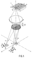
- Fig. 1 shows a small part of an
optical record carrier 1 with a radiation-reflectinginformation plane 2 and atransparent substrate 3. This Figure shows a number of tracks 4, separated or not separated byintermediate areas 5, for example grooves. The tracks extend in the X direction of a system of axes XYZ shown in the Figure, in which the information plane is parallel to the X-Y plane. The information is recorded on the record carrier in the form of optically readable areas, ordered in the tracks and having a width equal to or smaller than the width of the track. Fig. 1 shows some of these areas. The areas may have a shape of, for example pits or bumps or areas having a reflection different from that of its surroundings, or magnetic domains with a direction of magnetization different from that of its surroundings. The information plane is scanned by ascanning beam 6 emitted by aradiation source 7, for example a diode laser whose centre coincides with the origin O of the system of axes XYZ. This beam is focused on the information plane to a small scanning spot Sa by anobjective system 8 diagrammatically shown by means of a single lens. A separate collimator lens may precede the objective system. If the record carrier is disc-shaped, the tracks can be scanned by rotating the record carrier about an axis parallel to the Z axis. The entire information plane is scanned by moving the record carrier and the optical system of source, lens anddetection system 10 in the radial direction, i.e. the Y direction, with respect to each other. - It must be possible to detect the beam reflected by the information plane and modulated by the information and the track structure, for which purpose this beam must be separated from the scanning beam towards the information plane. To this end the device may be provided with a
diffraction element 12 in the form of a grating which deflects the reflected beam from the path of the projectedbeam 6. For the Foucault focus error detection the reflected beam must be split into two scanningsub-beams detection system 10 must comprise, for example two pairs ofdetection elements first pair first sub-beam 13 and thesecond pair second sub-beam 14. - As described in said United States Patent no. 4,665,310, the beam separation and the beam splitting can be performed by one diffraction element. This
element 12 splits the beam reflected by the information plane and passing through theobjective system 8 into a non-diffracted zero-order sub-beam and a plurality of sub-beams of the first and higher orders. Preferably, the first-order sub-beams are diffracted towards thedetector system 10. The part of the radiation emitted by thesource 7 and being incident on the detection system can be adjusted by a choice of the grating parameters notably the ratio between the width of the grating grooves and that of the areas between the grating grooves and the depth and the shape of the grooves. - The known grating 12 shown in Fig. 1 comprises two
sub-gratings dividing line 17 which is parallel to the X axis. The grating lines in each sub-grating shown in the Figure are parallel, while the lines of the first sub-grating extend at a first angle and those of the second sub-grating extend at a second, equally large but opposite angle to thedividing line 17. The grating lines of the gratings actually used often have a substantially hyperbolic shape and are substantially parallel. Such gratings may also have an optical strength, for example if there is a height difference between the radiation source and thedetection system 10. The sub-beams 13 and 14 diffracted by the sub-gratings 15 and 16 each have a direction substantially perpendicular to the grating lines of the associated sub-grating. The radiation spots S₁ and S₂ formed by the sub-beams 13 and 14 in the X-Y plane are offset with respect to each other in the Y direction and are located symmetrically with respect to the X axis. Thedetection system 10 for detecting the sub-beams comprises two detectors, one detector comprisingdetection elements bounding line 22, and one detector comprising thedetection elements bounding line 25. The detection elements are arranged in such a way that the centres of gravity of the radiation spots S₁ and S₂ are on therespective bounding lines scanning beam 6 is correctly focused on theinformation plane 2. When a focus error occurs, the centres of gravity of the radiation distribution of the spots S₁ and S₂ are displaced either towards or away from each other, dependent on the direction of the focus error. If the output signals of thedetection elements

This known method of generating the focus error signal is referred to as the double-Foucault method because of the detection of each sub-beam by means of a pair of detection elements. The signal which is proportional to the information which has been read, i.e. the information signal Si, is given by:

- It is found that the magnitude of the focus error signal Sf does not only depend on the magnitude of the focus error but also on the radial position of the scanning spot, i.e. the position in the Y direction. The cause of this radial to focus crosstalk will be elucidated with reference to Fig. 2. The
scanning beam 6 incident on theinformation plane 2 is not only reflected but also diffracted by the tracks in the information plane. The diffraction in the Y direction, i.e. perpendicular to the track direction, will hereinafter be considered. The diffraction results in a zero-order, two first-order and further, weaker higher-order beams being reflected from the information plane. The zero-order beam returns along the path of the incident beam. The first and higher-order beams are deflected in the Y direction perpendicular to the tracks extending in the X direction. The angle at which the beams are deflected is determined by the track period, while the strength is generally determined by the geometry of the tracks 4 and theintermediate areas 5 and by the geometry of the areas in which the information has been recorded. Fig. 2 shows the cross-section of the 0th, +1st and -1st order beams in the plane of theobjective system 8 by means of thereference numerals objective system 8 will be lost. The intensity of the radiation in the overlap areas of the oth and 1st order beam depends on the intensity of each beam individually and on the phase difference between the two beams. The phase difference is dependent on the position of the scanning spot Sa with respect to the tracks. When the scanning spot scans across the tracks in the Y direction, the phase difference between 0th and +1st-order beams and between the 0th and -1st-order beams changes continuously. Consequently, intensity differences arise between the overlap areas. These intensity variations allow the generation of a tracking error signal indicating how far the centre of the scanning spot is remote from the centreline of the track to be scanned. - The positions of the overlap areas at the location of the grating 12 are denoted by means of the
lines detection elements

The tracking error signal is maximum when thedividing line 17 of the grating 12 is parallel to the tracks 4 as is shown in Fig. 2. In that case all radiation in an overlap area of the 0th-order and a 1st-order beam bounded by thecircle 15 and thearcs line 17 and the effective track direction is larger than 0°, each detector will receive radiation from the two overlap areas. If the dividing line angle increases, the value of the tracking error signal St will decrease until the signal becomes zero at a dividing line angle of 90° at which each detector receives half the radiation from each overlap area. At a dividing line angle of 80° or less, a usable tracking error signal can still be generated. - The presence of the 0th and 1st-order diffraction beams in the beam which is split into the two sub-beams 13 and 14 by the grating 12 provides the possibility of generating a tracking error, but also causes the radial to focus crosstalk. Said phase differences in the overlap areas which are dependent on the tracking error cause, as it were, tilts or curvatures of the wavefronts of the +1st and -1st-order beams incident on the grating, causing variations in the angles at which the sub-beams 13 and 14 are diffracted by the grating. Consequently, the radiation spots S₁ and S₂ are offset transversely to the
bounding lines - The crosstalk is maximum in the configuration shown in which the
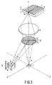
dividing line 17 is parallel to the tracks 4. If the dividing line angle is larger than 0°, each detector receives radiation from the two overlap areas and the crosstalk is found to be smaller. With a small increase of the dividing line angle from 0° the crosstalk decreases already rapidly so that with a dividing line angle of 15° the focus error signal has a quality which is already better than at 0°. In contrast to the general assumption, it has been found that the crosstalk is not minimum at a dividing line angle of 90°, but at a smaller angle. The size of the angle at which there is a minimum crosstalk is dependent on the geometry of the tracks and on the optical parameters of the radiating scanning beam. In accordance with the invention the dividing line angle is chosen in the range between 15° and 80°, with the additional advantage that a tracking error signal can be generated in the entire range by means of the push-pull method. - The crosstalk is also dependent on the distance between the detectors and the grating. It is found that this dependence is minimal if the dividing line angle is between 30° and 60°. This range has the additional advantage that the crosstalk itself is small in this range. The minimum crosstalk is around a dividing line angle of 45° for different devices and record carriers. An embodiment of the device according to the invention with a dividing line angle of 45° is shown in Fig. 3. The
detection system 10 for the scanning beam is shown as a unit of four juxtaposed detection elements. Similarly as in the devices shown in Figs. 1 and 2 and as known from European Patent Application no. 0 372 629, thebounding lines radiation source 7. This has been done with a view to possible changes of the wavelength of the radiation generated by the laser diode, which changes may be caused by, for example a change of the temperature of or of the current through the laser diode. Due to the wavelength-dependent behaviour of the grating 12 the radiation spots S₁ and S₂ are offset towards the point of convergence of the zero-order beam of the grating or away from this point when the wavelength is changed. The point of convergence of the zero-order beam coincides with the centre of theradiation source 7 in the configuration shown. A second effect of a change of the radiation wavelength is that the operation of the objective system is influenced. The resultant deviation in the focus error detection may be compensated for by giving the bounding lines slightly different directions than the lines through the centre of the radiation source. In some devices a satisfactory compensation is obtained when thebounding lines detection system 10 to the radiation source. Due to said choice of the direction of thebounding lines diffraction element 12, i.e. the Z axis in Fig. 3. - Fig. 4A is a plan view of the X-Y plane with the
detection system 10 and the projection of the grating 12 on the plane, the detection system and the grating having the same configuration as in the device shown in Fig. 3. The position of the overlap areas is denoted by means of thelines effective track direction 33 is denoted by a broken line. The dividing line angle is the angle of less than 90° between the effective track direction and thedividing line 17. Fig. 4B shows a modification of the configuration of Fig. 4A in which thedetection elements single detector 26. The focus error signal is generated only from the difference signal of the twodetection elements - The orientation of the grating 12 according to the invention is also applicable in a device in which the tracking of the scanning spot is realised by means of two extra beams. Such a device known per se from, inter alia the previously mentioned European Patent Application no. 0 372 629 is shown in Fig. 5. The two extra beams in this device are formed by a second diffraction element comprising a
single grating 30 which is arranged in the beam supplied by theradiation source 7. The substantially parallel, straight grating lines of the single grating extend at a small angle to the Y axis. The grating diffracts a +1st-order beam in approximately the +X direction and a -1st-order beam in the -X direction. These +1st and -1st-order beams constitute twoauxiliary beams scanning beam 6. The auxiliary beams 31 and 32 are focused to two radiation spots Sb and Sc on theinformation plane 2 by theobjective system 8. The two radiation spots extend in the X direction, i.e. the track direction at both sides of the radiation spots Sa formed by thescanning beam 6. Due to the small angle between the Y axis and the grating lines of the single grating, the radiation spots Sb and Sc will have small displacement in the -Y and +Y directions with respect to the radiation spot Sa. In the device shown in Fig. 5 the distance in the Y direction between the radiation spot Sa and each one of the radiation spots Sb and Sc is a quarter of the track period. A part of the radiation in the three beams reflected by the information plane is diffracted from the projected beams by thegrating 12. To avoid that the diffracted beams are split again by thesingle grating 30, thegratings grating 30. - The grating 12 treats each one of the reflected beams in the same way as described with reference to Fig. 4. A part of each beam is diffracted in the direction of the
detection system 10 and also split into two sub-beams. In the grating 12 shown in Fig. 5 this splitting into sub-beams is realised in a direction perpendicular to thedividing line 17 of the grating. In this way the reflectedscanning beam 6 is split to two sub-beams forming the two radiation spots S₁ and S₂ on thedetection system 10. Thedetection system 10 in Fig. 5 is subdivided into fourdetection elements auxiliary beam 31 is also split into two sub-beams by the grating 12, which sub-beams form two radiation spots S₃ and S₄ on adetection system 35. The spots S₃ and S₄ are mutually displaced in a direction perpendicular to thedividing line 17, while with respect to the spots S₁ and S₂ these spots are offset approximately parallel to the X axis. Analogously, the grating 12 forms two sub-beams from the reflectedauxiliary beam 32, which sub-beams form radiation spots S₅ and S₆ on adetection system 40. Twodetection systems detection system 35 and that ofdetection system 40 is a measure of the tracking error of the scanning spot Sa and can be used to keep the scanning spot on the centreline of the track to be scanned. - The orientation of the
dividing line 17 of the grating 12 at an acute angle to the direction of the tracks leads to a reduction of the radial to focus crosstalk, likewise as in the device shown in Fig. 4. A further advantage of this orientation of the grating 12 will be elucidated with reference to Fig. 6. Fig. 6A is a plan view of the X-Y plane with thedetection systems gratings single grating 30 are again approximately parallel to the Y axis so as to displace the radiation spots Sb and Sc in the X direction with respect to the radiation spot Sa. In the known device thedividing line 17 of the grating 12 is parallel to the tracks. The sub-beams diffracted by the grating 12 yield three pairs of radiation spots S₁-S₆ located one behind the other in the X direction. Thedetection systems - When the wavelength of the radiation emitted by the
diode laser 7 is changed, the radiation spots S₁-S₆ will be displaced in the X direction. The radiation spots S₁ and S₂ are then displaced along thebounding lines detection system 10. This length is fixed by the distances between the three pairs of radiation spots on the detection systems which in their turn are defined by requirements imposed on the distances between the radiation spots Sa, Sb and Sc on theinformation plane 2. Due to these requirements, the length of the detection systems cannot be freely chosen and wavelength variations and detector positioning have a small tolerance. In a device according to the invention the toleances may be considerably wider due to said orientation of thedividing line 17 of the grating with respect to the tracks. - Fig. 6B shows a configuration according to the invention of the
gratings detection systems gratings detection systems detection system 10 in a direction perpendicular to the connection line between the centre of thedetection system 10 and the point of convergence of the zero-order beam of the grating 12, i.e. the centre of the grating 12 in Fig. 6B. It is now possible to choose the length of the detection systems parallel to the connection line as large as is necessary for positioning tolerances of the detection systems and gratings and for the displacements of the radiation spots due to wavelength changes. The detection systems may be arranged further apart in the case of a larger dividing line angle. At a dividing angle around 45° the distance between detection systems is large enough to use elongate detection elements, while there is a small crosstalk and a usable tracking error signal can be generated by means of the push-pull method. In Fig. 6B the detection system has two boundinglines bounding lines - The grating lines in the sub-gratings 15 and 16 of the grating 12 need not necessarily be symmetrical with respect to the
dividing line 17. Fig. 6D shows a configuration with a grating 12' in which the grating lines in the two sub-gratings are parallel to each other and the period of the grating lines in the sub-grating 15' is larger than in the sub-grating 16'. The sub-beams formed by the sub-grating 15' will be diffracted at a smaller angle than the sub-beams formed by the sub-grating 16'. The radiation spot S₂ formed by the scanning sub-beam from the sub-grating 16' is therefore located further away from the centre of the grating 12' than the radiation spot S₁ generated by the scanning sub-beam from the sub-grating 15'. The displacement of the auxiliary beams in the X direction by thesingle grating 30 ensures that the radiation spots S₃ and S₄, S₅ and S₆ offset in the X direction are located at both sides of the radiation spots S₁ and S₂. Consequently, thedetection systems - The
detection system 10 in Fig. 6D has only one pair ofdetection elements - For scanning some types of information planes, the tracking error signal generated by means of the two
auxiliary beam 6 described with reference to Fig. 5 is too small to realise a satisfactory tracking. Then it is often possible to generate a satisfactory tracking error signal by applying the push-pull method to each one of the twoauxiliary beams scanning beam 6. This three-beam push-pull method, also referred to as differential push-pull, is known per se from European Patent Application no. 0 409 469. Fig. 7 shows a device according to the invention in which the tracking error signal is generated by means of the three-beam push-pull method. The angle at which the grating lines of thesingle grating 30 extends to the Y axis in this device is chosen to be slightly larger than in the device shown in Fig. 5 so that the radiation spots Sb and Sc on theinformation plane 2 are located in the Y direction at a distance which is equal to half a track period of the radiation spot Sa. A maximum tracking error signal can be generated at this distance between the radiation spots. To be able to detect each radiation spot S₃, S₄, S₅ and S₆ individually, eachdetection system detectors detectors

in which C is a constant which is dependent on the intensity difference between the scanning beam and the auxiliary beams. - The only bounding line between the detectors in the
detection systems lines detection system 10 each dividing a radiation spot in half and with which the focus error signal is generated. If one of these bounding lines is omitted, the focus error signal can be generated by means of the single-Foucault method. The device shown in Fig. 7 has said advantages of a minor radial to focus crosstalk and a wide tolerance for offsets of the radiation spots due to wavelength changes. - For a satisfactory tracking it is desired in some devices to locate the radiation spots Sa, Sb and Sc relatively close together on the information plane. Consequently, the radiation spots S₃, S₁ and S₅ as well as the radiation spots S₄, S₂ and S₆ on the detection systems in Fig. 7 are located relatively close together. As a result, the separate detectors have to be so narrow that the alignment of the optical system is impeded. Therefore, a detector configuration as shown in Fig. 8 is preferably used in such devices. The three radiation spots S₃, S₁ and S₅ formed by the sub-beams diffracted by the sub-grating 15'' are located on the juxtaposed
detectors detectors - The devices described so far have a grating 12 which is radiation transmissive. However, the present invention is also applicable in a device having a radiation-reflecting grating. An embodiment of such a device as shown in Fig. 9. This device comprises an optical system which is comparable to that of the device shown in Fig. 3. The
radiation source 7 supplies a diverging beam with its chief ray parallel to the X axis. The beam is incident on a grating 45 which is arranged at an angle of 45° to the X axis. The beam reflected by the grating subsequently traverses theobjective system 8 in the Z direction, which system focuses the beam on theinformation plane 2. The beam reflected by the information plane is subsequently diffracted in a 0th, +1st and -1st-order by thegrating 45. The 0th-order beam returns to thelaser 7 and the two first-order sub-beams are diffracted towards thedetection system 10. The radiation-sensitive surface of thedetection system 10 and the radiation-emitting surface of theradiation source 7 are located in a plane parallel to the Y-Z plane, offset in the +X direction. Theconnection line 50 between the centre of the detection system and the centre of the laser diode extends at an angle of 45° to both the Y axis and the Z axis. The detection system is divided into fourdetection elements sub-gratings dividing line 46. The orientation of the dividing line is shown by means of a broken line indicating theeffective track direction 51. The angle between the dividingline 17 and thebroken line 51 should be between 15° and 80° according to the invention and is approximately equal to 45° in the Figure. The reflectinggrating 45 provides the possibility of a very compact construction of the device. The invention may also be used in a device having a reflecting grating 30 or a device in which the twogratings - Although the sub-gratings of the
gratings - In the embodiments of the device according to the invention described so far, the sub-beams are generated by means of a grating as a dividing element. However, the invention is not limited thereto but is applicable in all devices in which the beam from the information plane is divided into two sub-beams by means of a dividing line. For example, it is possible to use a slightly prismatic dividing plate as a dividing element. Each of the two sub-areas of the dividing element then comprises a face of the prism. The dividing plate is arranged in the beam going towards the detection system. An advantage of the dividing plate is that the direction of the sub-beams is hardly dependent on the wavelength of the radiation.
- The focus error signal in the devices shown is generated by means of the single or double-Foucault method. The invention is also applicable in devices in which the focus error signal is generated by means of the beam-size method which is known per se from United States Patent no. 4,724,533. The
scanning sub-beams - Fig. 10A shows a dividing element in the form of a
prismatic dividing plate 55. The dividing plate has two prism faces 56 and 57 which are separated by dividingline 58. According to the invention, the angle between the dividingline 58 and theeffective track direction 51 is between 15° and 80°. The normals on thefaces prism face 56 is focused above the plane of thedetection system 10, while the sub-beam formed by theprism face 57 is focused below the plane. This difference in height of the focal points can be realised by giving the prism faces 56 and 57 different optical strengths, for example by giving the faces a different curvature. The sub-beam formed by theface 56 forms aradiation spot 59 on thedetector 60 comprising threedetection elements face 57 forms aradiation spot 64 on thedetector 65 comprising threedetection elements detectors detection system 10. The width of thecentral detection elements radiation spot 64 or 69 if this spot is focused in the plane of the detection system. The Figure shows the situation in which thescanning beam 6 is focused on theinformation plane 2 and the radiation spots 59 and 64 are thus equally large. Generally, the dividingplate 55 will be arranged in the beam between a beam splitter and a detection system, the beam splitter deflecting a part of the radiation reflected by the record carrier towards the detection system, and the centre of the dividing plate and the detection system will be located on the optical axis of the beam. For the sake of clarity, the detection system and the dividing plate are shown next to each other instead of on top of each other in Fig. 10. The focus error signal Sf' is then given by:

- Fig. 10B shows a dividing element in the form of a diffraction element and an associated detection system for use of the beam-size method in a device as shown in Fig. 3. The
diffraction element 70 comprises twosub-gratings bounding line 73. Each sub-grating has curved grating lines and a different optical strength. The sub-beam formed by sub-grating 71 is focused below the plane of thedetection system 10 and forms aradiation spot 75 on thedetector 60 comprising twodetector elements detection sytem 10 and forms aradiation spot 78 on thedetector 65 comprising twodetection elements

- It will be evident that said embodiments of the device in which a focus error signal is generated by means of the beam-size method can be combined with the generation of a tracking error signal in accordance with the push-pull method or by means of two auxiliary beams.
Claims (11)
- A device for optically scanning tracks (4) in a radiation-reflecting information plane (2), which device comprises a radiation source (7) for supplying a scanning beam (6), an objective system (8) for focusing the scanning beam to a scanning spot (Sa) on the information plane, a dividing element (12, 55) comprising two sub-areas (15, 16) located symmetrically at both sides of a dividing line (17) and arranged in the optical path of the radiation from the information plane for splitting at least a part of said radiation into two scanning sub-beams (13, 14), and a radiation-sensitive detection system (10), characterized in that the angle between the dividing line and the effective track direction is between 15° and 80°.
- A device as claimed in Claim 1, characterized in that the angle is between 30° and 60°.
- A device as claimed in Claim 1 or 2, characterized in that the dividing element is a prismatic dividing plate (55) in which each sub-area consists of a prism face (56, 57).
- A device as claimed in Claim 1 or 2, characterized in that the dividing element is a diffraction element (12), in which each sub-area consists of a sub-grating (15, 16).
- A device as claimed in any one of Claims 1 to 4, characterized in that a further diffraction element (30) having substantially straight grating lines is arranged in the optical path of the scanning beam (6) between the radiation source (7) and the objective system (8) for splitting the beam emitted by the radiation source into the scanning beam and two auxiliary beams (31, 32), which auxiliary beams are focused by the objective system to two further radiation spots (Sb, Sc) on the information plane (2), and in that the device comprises two further detection systems (35, 40) each being associated with one of the auxiliary beams reflected by the information plane.
- A device as claimed in Claim 5, characterized in that the detection systems (35, 40) for the auxiliary beams (31, 32) are located at both sides of the detection system (10) for the scanning beam (6) in a direction transverse to the perpendicular from the centre of the detection system (10) for the scanning beam to the optical axis of the zero-order beam of the diffraction element (12).
- A device as claimed in Claim 5, characterized in that the detection systems (10, 35, 40) for the scanning beam (6), the first auxiliary beam (31) and the second auxiliary beam (32) comprise a first and second (43, 44), a third and fourth (36, 37), and a fifth and sixth detector (41, 42), respectively, the six detectors being juxtaposed in the sequence: three, one, five, four, two, six, viewed in a direction transverse to the perpendicular from the centre of the detection system (10) for the scanning beam to the optical axis of the zero-order beam of the diffraction element (12'').
- A device as claimed in any one of Claims 1 to 7, characterized in that the detection system (10) for the scanning beam (6) comprises two detectors, at least one of which is divided by means of a bounding line (22) into two detection elements (20, 21) for detecting a scanning sub-beam (13).
- A device as claimed in Claim 8, characterized in that the bounding line (22) between the detection elements (20, 21) is substantially directed towards the optical axis of the zero-order beam of the diffraction element (12).
- A device as claimed in any one of Claims 1 to 9, characterized in that the sub-areas (56, 57; 71, 72) have different optical strengths.
- A device as claimed in any one of Claims 1 to 10, characterized in that the dividing element (12, 12', 12'', 45, 55, 70) and/or the further diffraction element (30) are reflecting.
Priority Applications (1)
| Application Number | Priority Date | Filing Date | Title |
|---|---|---|---|
| EP19930202341 EP0583036B1 (en) | 1992-08-12 | 1993-08-09 | Device for optically scanning a surface |
Applications Claiming Priority (3)
| Application Number | Priority Date | Filing Date | Title |
|---|---|---|---|
| EP92202487 | 1992-08-12 | ||
| EP92202487 | 1992-08-12 | ||
| EP19930202341 EP0583036B1 (en) | 1992-08-12 | 1993-08-09 | Device for optically scanning a surface |
Publications (3)
| Publication Number | Publication Date |
|---|---|
| EP0583036A2 true EP0583036A2 (en) | 1994-02-16 |
| EP0583036A3 EP0583036A3 (en) | 1994-04-20 |
| EP0583036B1 EP0583036B1 (en) | 1998-07-15 |
Family
ID=26131630
Family Applications (1)
| Application Number | Title | Priority Date | Filing Date |
|---|---|---|---|
| EP19930202341 Expired - Lifetime EP0583036B1 (en) | 1992-08-12 | 1993-08-09 | Device for optically scanning a surface |
Country Status (1)
| Country | Link |
|---|---|
| EP (1) | EP0583036B1 (en) |
Cited By (13)
| Publication number | Priority date | Publication date | Assignee | Title |
|---|---|---|---|---|
| EP0676750A2 (en) * | 1994-04-08 | 1995-10-11 | Lg Electronics Inc. | Optical pickup system |
| WO1995034016A1 (en) * | 1994-06-07 | 1995-12-14 | Philips Electronics N.V. | Optical beam-splitting element |
| WO1996036006A1 (en) * | 1995-05-08 | 1996-11-14 | Philips Electronics N.V. | Optical reader and optical information scanning device comprising such a reader |
| US5708638A (en) * | 1995-03-15 | 1998-01-13 | U.S. Philips Corporation | Device for optically scanning a recording medium by focusing the best focus or the paraxial focus to the information layer |
| US5757744A (en) * | 1995-07-31 | 1998-05-26 | U.S. Philips Corporation | Optical scanning apparatus for a multi-layer record carrier, including a focus control circuit |
| WO1999024974A2 (en) * | 1997-11-07 | 1999-05-20 | Koninklijke Philips Electronics N.V. | Optical scanning device |
| US6108138A (en) * | 1994-06-07 | 2000-08-22 | U.S. Philips Corporation | Optical beam shaper, and radiation source unit and scanning device including said beam shaper |
| EP1109163A2 (en) * | 1999-12-16 | 2001-06-20 | Victor Company Of Japan, Ltd. | Optical device |
| US6483650B1 (en) | 1998-08-04 | 2002-11-19 | Sony Corporation | Integrated optical element, optical pickup, and optical disk device |
| US6512732B1 (en) | 1995-12-21 | 2003-01-28 | Koninklijke Philips Electronics N.V. | Device for optically scanning information tracks on a plane using two subbeams |
| EP1341166A2 (en) * | 2002-02-27 | 2003-09-03 | Ricoh Company, Ltd. | Optical pickup for different wavelengths |
| EP1351227A1 (en) * | 2001-01-12 | 2003-10-08 | Sony Corporation | Optical pickup and optical disc drive |
| WO2006064437A3 (en) * | 2004-12-16 | 2006-08-31 | Koninkl Philips Electronics Nv | A method for measuring and optimizing radial to vertical crosstalk |
Citations (5)
| Publication number | Priority date | Publication date | Assignee | Title |
|---|---|---|---|---|
| EP0228620A2 (en) * | 1985-12-10 | 1987-07-15 | Nec Corporation | Optical head comprising a diffraction grating for directing two or more diffracted beams to optical detectors |
| EP0300570A1 (en) * | 1987-07-24 | 1989-01-25 | Koninklijke Philips Electronics N.V. | Apparatus for optically scanning an information plane |
| EP0372629A2 (en) * | 1988-12-05 | 1990-06-13 | Koninklijke Philips Electronics N.V. | Apparatus for optically scanning an information plane |
| JPH0554411A (en) * | 1991-08-23 | 1993-03-05 | Sharp Corp | Optical information recording/reproducing device |
| EP0554092A1 (en) * | 1992-01-28 | 1993-08-04 | Sharp Kabushiki Kaisha | An optical information recording and reproducing device |
-
1993
- 1993-08-09 EP EP19930202341 patent/EP0583036B1/en not_active Expired - Lifetime
Patent Citations (5)
| Publication number | Priority date | Publication date | Assignee | Title |
|---|---|---|---|---|
| EP0228620A2 (en) * | 1985-12-10 | 1987-07-15 | Nec Corporation | Optical head comprising a diffraction grating for directing two or more diffracted beams to optical detectors |
| EP0300570A1 (en) * | 1987-07-24 | 1989-01-25 | Koninklijke Philips Electronics N.V. | Apparatus for optically scanning an information plane |
| EP0372629A2 (en) * | 1988-12-05 | 1990-06-13 | Koninklijke Philips Electronics N.V. | Apparatus for optically scanning an information plane |
| JPH0554411A (en) * | 1991-08-23 | 1993-03-05 | Sharp Corp | Optical information recording/reproducing device |
| EP0554092A1 (en) * | 1992-01-28 | 1993-08-04 | Sharp Kabushiki Kaisha | An optical information recording and reproducing device |
Non-Patent Citations (1)
| Title |
|---|
| PATENT ABSTRACTS OF JAPAN vol. 17, no. 366 (P-1571)9 July 1993 & JP-A-05 054 411 (SHARP CORP) 5 March 1993 * |
Cited By (24)
| Publication number | Priority date | Publication date | Assignee | Title |
|---|---|---|---|---|
| EP0676750A2 (en) * | 1994-04-08 | 1995-10-11 | Lg Electronics Inc. | Optical pickup system |
| EP0676750A3 (en) * | 1994-04-08 | 1996-10-16 | Lg Electronics Inc | Optical pickup system. |
| WO1995034016A1 (en) * | 1994-06-07 | 1995-12-14 | Philips Electronics N.V. | Optical beam-splitting element |
| US5608708A (en) * | 1994-06-07 | 1997-03-04 | U.S. Philips Corporation | Optical beam-splitting element |
| US6108138A (en) * | 1994-06-07 | 2000-08-22 | U.S. Philips Corporation | Optical beam shaper, and radiation source unit and scanning device including said beam shaper |
| US5708638A (en) * | 1995-03-15 | 1998-01-13 | U.S. Philips Corporation | Device for optically scanning a recording medium by focusing the best focus or the paraxial focus to the information layer |
| WO1996036006A1 (en) * | 1995-05-08 | 1996-11-14 | Philips Electronics N.V. | Optical reader and optical information scanning device comprising such a reader |
| US5757744A (en) * | 1995-07-31 | 1998-05-26 | U.S. Philips Corporation | Optical scanning apparatus for a multi-layer record carrier, including a focus control circuit |
| US5793721A (en) * | 1995-07-31 | 1998-08-11 | U.S. Philips Corporation | Optical scanning apparatus for a multi-layer record carrier, including a focus control circuit |
| US6512732B1 (en) | 1995-12-21 | 2003-01-28 | Koninklijke Philips Electronics N.V. | Device for optically scanning information tracks on a plane using two subbeams |
| WO1999024974A2 (en) * | 1997-11-07 | 1999-05-20 | Koninklijke Philips Electronics N.V. | Optical scanning device |
| WO1999024974A3 (en) * | 1997-11-07 | 1999-07-15 | Koninkl Philips Electronics Nv | Optical scanning device |
| US6483650B1 (en) | 1998-08-04 | 2002-11-19 | Sony Corporation | Integrated optical element, optical pickup, and optical disk device |
| EP1109163A2 (en) * | 1999-12-16 | 2001-06-20 | Victor Company Of Japan, Ltd. | Optical device |
| EP1109163A3 (en) * | 1999-12-16 | 2003-07-09 | Victor Company Of Japan, Ltd. | Optical device |
| US6891675B2 (en) | 1999-12-16 | 2005-05-10 | Victor Company Of Japan, Limited | Optical device |
| EP1351227A1 (en) * | 2001-01-12 | 2003-10-08 | Sony Corporation | Optical pickup and optical disc drive |
| EP1351227A4 (en) * | 2001-01-12 | 2005-02-09 | Sony Corp | Optical pickup and optical disc drive |
| US6987614B2 (en) | 2001-01-12 | 2006-01-17 | Sony Corporation | Optical pickup and optical disc drive device |
| EP1341166A2 (en) * | 2002-02-27 | 2003-09-03 | Ricoh Company, Ltd. | Optical pickup for different wavelengths |
| EP1341166A3 (en) * | 2002-02-27 | 2005-02-09 | Ricoh Company, Ltd. | Optical pickup for different wavelengths |
| US7142497B2 (en) | 2002-02-27 | 2006-11-28 | Ricoh Company, Ltd. | Optical pickup and optical information processing apparatus with light sources of three different wavelengths |
| US7848209B2 (en) | 2002-02-27 | 2010-12-07 | Ricoh Company, Ltd. | Optical pickup and optical information processing apparatus with light sources of three different wavelengths |
| WO2006064437A3 (en) * | 2004-12-16 | 2006-08-31 | Koninkl Philips Electronics Nv | A method for measuring and optimizing radial to vertical crosstalk |
Also Published As
| Publication number | Publication date |
|---|---|
| EP0583036B1 (en) | 1998-07-15 |
| EP0583036A3 (en) | 1994-04-20 |
Similar Documents
| Publication | Publication Date | Title |
|---|---|---|
| CA1263183A (en) | Apparatus for optically scanning an information plane | |
| US5684762A (en) | Opto-magnetic head apparatus | |
| KR880001707B1 (en) | Opto-electronic focusing error detection device | |
| JP2683918B2 (en) | Device for optically scanning the information surface | |
| EP0201603A1 (en) | System for detecting tracking error of an optical head | |
| US4525826A (en) | Optical track position detecting apparatus and optical information processor using the same | |
| US5579298A (en) | Optical scanner having symmetry about an oblique divider | |
| EP0583036B1 (en) | Device for optically scanning a surface | |
| US5608695A (en) | Optical pick-up apparatus with tracking error detection by detection of amount of light in fan field | |
| US4924082A (en) | Optical scanning device, mirror objective suitable for use in said device and optical write and/or read apparatus provided with said device | |
| KR100238737B1 (en) | Apparatus for optically scanning a radiation-reflecting information | |
| JPH0775080B2 (en) | Optical scanning device | |
| US5754503A (en) | Optical device with improved focused error detection and tracing error detection for optical disk drive | |
| US6256285B1 (en) | Optical scanning device | |
| US6407973B1 (en) | Device for scanning an optical record carrier having at least two information layers | |
| US6512732B1 (en) | Device for optically scanning information tracks on a plane using two subbeams | |
| US6567353B1 (en) | Optical head with light receiving element surfaces divided into at least three light receiving areas | |
| US5144131A (en) | Device for optically scanning an information plane detecting border portions of light beam | |
| EP0273422B1 (en) | A method and apparatus for detecting track and focus errors in an optical head | |
| JP2594445B2 (en) | Hologram optical head | |
| EP0336737A2 (en) | Optical information reading apparatus | |
| US5150342A (en) | Photo-detecting device | |
| JP3044667B2 (en) | Optical reader | |
| JP3694206B2 (en) | Optical information recording / reproducing head device | |
| JP2734685B2 (en) | Photodetector adjustment method and focus error detection device |
Legal Events
| Date | Code | Title | Description |
|---|---|---|---|
| PUAI | Public reference made under article 153(3) epc to a published international application that has entered the european phase |
Free format text: ORIGINAL CODE: 0009012 |
|
| AK | Designated contracting states |
Kind code of ref document: A2 Designated state(s): AT DE FR GB IT |
|
| PUAL | Search report despatched |
Free format text: ORIGINAL CODE: 0009013 |
|
| AK | Designated contracting states |
Kind code of ref document: A3 Designated state(s): AT DE FR GB IT |
|
| RAP1 | Party data changed (applicant data changed or rights of an application transferred) |
Owner name: N.V. PHILIPS' GLOEILAMPENFABRIEKEN |
|
| 17P | Request for examination filed |
Effective date: 19941019 |
|
| 17Q | First examination report despatched |
Effective date: 19961125 |
|
| GRAG | Despatch of communication of intention to grant |
Free format text: ORIGINAL CODE: EPIDOS AGRA |
|
| GRAG | Despatch of communication of intention to grant |
Free format text: ORIGINAL CODE: EPIDOS AGRA |
|
| GRAH | Despatch of communication of intention to grant a patent |
Free format text: ORIGINAL CODE: EPIDOS IGRA |
|
| GRAH | Despatch of communication of intention to grant a patent |
Free format text: ORIGINAL CODE: EPIDOS IGRA |
|
| GRAA | (expected) grant |
Free format text: ORIGINAL CODE: 0009210 |
|
| AK | Designated contracting states |
Kind code of ref document: B1 Designated state(s): AT DE FR GB IT |
|
| REF | Corresponds to: |
Ref document number: 168491 Country of ref document: AT Date of ref document: 19980815 Kind code of ref document: T |
|
| REF | Corresponds to: |
Ref document number: 69319673 Country of ref document: DE Date of ref document: 19980820 |
|
| RAP4 | Party data changed (patent owner data changed or rights of a patent transferred) |
Owner name: KONINKLIJKE PHILIPS ELECTRONICS N.V. |
|
| ET | Fr: translation filed | ||
| PLBE | No opposition filed within time limit |
Free format text: ORIGINAL CODE: 0009261 |
|
| STAA | Information on the status of an ep patent application or granted ep patent |
Free format text: STATUS: NO OPPOSITION FILED WITHIN TIME LIMIT |
|
| 26N | No opposition filed | ||
| REG | Reference to a national code |
Ref country code: GB Ref legal event code: IF02 |
|
| PGFP | Annual fee paid to national office [announced via postgrant information from national office to epo] |
Ref country code: GB Payment date: 20040811 Year of fee payment: 12 |
|
| PGFP | Annual fee paid to national office [announced via postgrant information from national office to epo] |
Ref country code: AT Payment date: 20040827 Year of fee payment: 12 |
|
| PGFP | Annual fee paid to national office [announced via postgrant information from national office to epo] |
Ref country code: FR Payment date: 20040830 Year of fee payment: 12 |
|
| REG | Reference to a national code |
Ref country code: GB Ref legal event code: 746 Effective date: 20040811 |
|
| PGFP | Annual fee paid to national office [announced via postgrant information from national office to epo] |
Ref country code: DE Payment date: 20041015 Year of fee payment: 12 |
|
| REG | Reference to a national code |
Ref country code: FR Ref legal event code: D6 |
|
| PG25 | Lapsed in a contracting state [announced via postgrant information from national office to epo] |
Ref country code: IT Free format text: LAPSE BECAUSE OF NON-PAYMENT OF DUE FEES;WARNING: LAPSES OF ITALIAN PATENTS WITH EFFECTIVE DATE BEFORE 2007 MAY HAVE OCCURRED AT ANY TIME BEFORE 2007. THE CORRECT EFFECTIVE DATE MAY BE DIFFERENT FROM THE ONE RECORDED. Effective date: 20050809 Ref country code: GB Free format text: LAPSE BECAUSE OF NON-PAYMENT OF DUE FEES Effective date: 20050809 Ref country code: AT Free format text: LAPSE BECAUSE OF NON-PAYMENT OF DUE FEES Effective date: 20050809 |
|
| PG25 | Lapsed in a contracting state [announced via postgrant information from national office to epo] |
Ref country code: DE Free format text: LAPSE BECAUSE OF NON-PAYMENT OF DUE FEES Effective date: 20060301 |
|
| GBPC | Gb: european patent ceased through non-payment of renewal fee |
Effective date: 20050809 |
|
| PG25 | Lapsed in a contracting state [announced via postgrant information from national office to epo] |
Ref country code: FR Free format text: LAPSE BECAUSE OF NON-PAYMENT OF DUE FEES Effective date: 20060428 |
|
| REG | Reference to a national code |
Ref country code: FR Ref legal event code: ST Effective date: 20060428 |