EP0571214A1 - An apparatus and a method for inputting/outputting an image - Google Patents
An apparatus and a method for inputting/outputting an image Download PDFInfo
- Publication number
- EP0571214A1 EP0571214A1 EP93303945A EP93303945A EP0571214A1 EP 0571214 A1 EP0571214 A1 EP 0571214A1 EP 93303945 A EP93303945 A EP 93303945A EP 93303945 A EP93303945 A EP 93303945A EP 0571214 A1 EP0571214 A1 EP 0571214A1
- Authority
- EP
- European Patent Office
- Prior art keywords
- image
- image input
- light
- transparent
- transparent substrate
- Prior art date
- Legal status (The legal status is an assumption and is not a legal conclusion. Google has not performed a legal analysis and makes no representation as to the accuracy of the status listed.)
- Granted
Links
Images


Classifications
-
- H—ELECTRICITY
- H04—ELECTRIC COMMUNICATION TECHNIQUE
- H04N—PICTORIAL COMMUNICATION, e.g. TELEVISION
- H04N1/00—Scanning, transmission or reproduction of documents or the like, e.g. facsimile transmission; Details thereof
- H04N1/024—Details of scanning heads ; Means for illuminating the original
- H04N1/028—Details of scanning heads ; Means for illuminating the original for picture information pick-up
- H04N1/02805—Details of scanning heads ; Means for illuminating the original for picture information pick-up with photodetectors arranged in a two-dimensional array
-
- G—PHYSICS
- G02—OPTICS
- G02F—OPTICAL DEVICES OR ARRANGEMENTS FOR THE CONTROL OF LIGHT BY MODIFICATION OF THE OPTICAL PROPERTIES OF THE MEDIA OF THE ELEMENTS INVOLVED THEREIN; NON-LINEAR OPTICS; FREQUENCY-CHANGING OF LIGHT; OPTICAL LOGIC ELEMENTS; OPTICAL ANALOGUE/DIGITAL CONVERTERS
- G02F1/00—Devices or arrangements for the control of the intensity, colour, phase, polarisation or direction of light arriving from an independent light source, e.g. switching, gating or modulating; Non-linear optics
- G02F1/01—Devices or arrangements for the control of the intensity, colour, phase, polarisation or direction of light arriving from an independent light source, e.g. switching, gating or modulating; Non-linear optics for the control of the intensity, phase, polarisation or colour
- G02F1/13—Devices or arrangements for the control of the intensity, colour, phase, polarisation or direction of light arriving from an independent light source, e.g. switching, gating or modulating; Non-linear optics for the control of the intensity, phase, polarisation or colour based on liquid crystals, e.g. single liquid crystal display cells
- G02F1/133—Constructional arrangements; Operation of liquid crystal cells; Circuit arrangements
- G02F1/135—Liquid crystal cells structurally associated with a photoconducting or a ferro-electric layer, the properties of which can be optically or electrically varied
- G02F1/1354—Liquid crystal cells structurally associated with a photoconducting or a ferro-electric layer, the properties of which can be optically or electrically varied having a particular photoconducting structure or material
-
- H—ELECTRICITY
- H04—ELECTRIC COMMUNICATION TECHNIQUE
- H04N—PICTORIAL COMMUNICATION, e.g. TELEVISION
- H04N1/00—Scanning, transmission or reproduction of documents or the like, e.g. facsimile transmission; Details thereof
- H04N1/024—Details of scanning heads ; Means for illuminating the original
- H04N1/028—Details of scanning heads ; Means for illuminating the original for picture information pick-up
Definitions
- the present invention relates to an image input/output apparatus and an image input/output method. More particularly, the present invention relates to an image input/output apparatus in which an image display section and an image input section are integrated into a unit, so that the apparatus is miniaturized and the construction of the apparatus is simplified. The present invention also relates to an image input/output method using the image input/output apparatus.
- FIG. 6 shows an exemplary active matrix type liquid crystal display apparatus.
- one of liquid crystal portions 251, 252, and one of thin film transistors (TFTs) 241, 242, ... are paired so as to constitute a pixel.
- the TFTs in respective rows are turned on or off by a gate drive circuit 200 via corresponding gate lines 211, 212, ....
- data (voltage) is sequentially written into the respective liquid crystal portions 251, 252, ... by a data drive circuit 202 via corresponding data lines 231, 232, ..., so as to perform a display.
- a contact type image sensor As an image input apparatus, a contact type image sensor is known.
- the contact type image sensor a one-dimensional sensor array is made so as to have a length which is equal to the width of an original, and the reflected light from the original is detected by the respective sensors in the sensor array.
- the image sensor or the original When a two-dimensional original is to be read by the contact type image sensor, the image sensor or the original is required to be mechanically moved in a direction perpendicular to the sensor array for scanning.
- a structure such as that shown in Figure 7 is proposed.
- pairs of photodetective layers 315 and TFTs 311 are provided in a matrix form on a transparent substrate 301 (for simplicity, only one pair of which is shown in Figure 7).
- a transparent protecting layer 302 is formed over the entire surface of the transparent substrate 301. Then, a thin glass plate 303 is Provided on the transparent protecting layer 302.
- an original 313 is illuminated by light 312 incident from the side on which the transparent substrate 301 is provided. Then, the reflected light 314 from the original 313 is detected by the photodetective layer 315 which converts the detected light into an electric signal.
- the converted electric signal is supplied via the TFTs to a scanning circuit (not shown), and taken out by the scanning circuit as a time-series signal.
- the image display and the image input are separately performed by different types of apparatus.
- a display is provided independently of an image reader and a scanner. The connection therebetween is realized via an interface.
- the image input/output apparatus of this invention includes: an image display section which selectively transmits light; and an image input section having a photodetective portion for converting part of the light which has been transmitted through the image display section and reflected from an original, into an electric signal.
- the image display section includes: a first transparent substrate; a second transparent substrate which is opposite to the first transparent substrate; a liquid crystal portion which is sandwiched between the first transparent substrate and the second transparent substrate; a plurality of pixel electrodes disposed in a matrix form, the plurality of pixel electrodes being disposed on a surface of the first transparent substrate on a side where the liquid crystal portion is provided; a counter electrode disposed on a surface of the second transparent substrate on a side where the liquid crystal portion is provided; and means for selectively applying voltage to at least desired one of the plurality of pixel electrodes.
- the photodetective portion is disposed on a portion of the second transparent substrate, the portion corresponding to a portion of the first transparent substrate where the plurality of pixel electrodes are not disposed.
- the photodetective portion includes: a lower electrode capable of blocking light; a photo-electric converting element formed on the lower electrode; and an upper electrode formed on the photo-electric converting element.
- each of the lower electrode and the upper electrode is a single portion with electric continuity.
- each of the lower electrode and the upper electrode is divided into a plurality of blocks which are electrically separated from each other.
- an image input/output apparatus includes: a pair of transparent substrates with liquid crystal sandwiched therebetween; transparent electrodes which constitute pixels, the transparent electrodes being provided on a inner surface of one of the pair of transparent substrates; means for selectively applying voltage to the transparent electrodes; a photodetective portion provided on the other one of the pair of transparent substrates on a side on which the liquid crystal is not formed; and a transparent layer which covers the photodetective portion.
- a method for inputting/outputting an image uses the image input/output apparatus according to the invention, and includes the steps of: sequentially applying voltage to at least any desired one of said plurality of pixel electrodes while irradiating said image display section with light, to selectively transmit part of light for scanning said original; and receiving light reflected from said original by said photodetective portion, to sequentially convert said received light into an electric signal by said photo-electric converting element.
- an image display section and an image input section are constructed into a unit, so that the apparatus is miniaturized. Moreover, since the image display and the image input can be performed by a single scanning circuit, the construction of the apparatus is simplified.
- the photodetective portion is formed in an area corresponding to gaps between pixels in the image display section, the light which is transmitted through the image display section will not be blocked by the photodetective portion. Therefore, the contrast for image display and image input is improved.
- the invention described herein makes possible the advantages of (1) providing an image input/output apparatus in which an image display section and an image input section are integrated into a unit, so that the apparatus is miniaturized and the construction of the apparatus can be simplified, and (2) providing an image input/output method which uses the image input/output apparatus.
- Figure 1 is a view showing a cross-sectional structure of an image input/output apparatus in one example according to the invention.
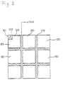
- Figure 2 shows a pattern of pixels and a photodetective portion in the image input/output apparatus according to the invention.
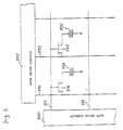
- FIG. 3 is a diagram showing an equivalent circuit of the image input/output apparatus according to the invention.
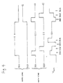
- Figure 4 is a diagram for explaining a scanning method during an image input of the image input/output apparatus according to the invention.
- Figure 5 shows a modified pattern of the photodetective portion according to the invention.
- Figure 6 is a diagram showing an equivalent circuit of a conventional active matrix type liquid crystal display apparatus.
- Figure 7 is a view showing a cross-sectional structure of a conventional image input apparatus.
- Figures 1 and 2 show a cross-sectional structure and a schematic pattern of an image input/output apparatus in one example according to the invention, respectively.
- the image input/output apparatus includes an image display section (an active matrix type liquid crystal display device) 10 and an image input section 20.
- the image display section 10 includes a pair of transparent substrates 100 and 106 with a ferroelectric liquid crystal 107 sandwiched therebetween.
- a transparent electrode 105 having a predetermined pattern which constitutes a pixel 120, and a transparent electrode 108 are disposed.
- the transparent electrodes 105 and 108 are made of ITO (indium tin oxide) films.
- a thin film transistor (TFT) 101 is formed for each of the pixels 120.
- the TFT 101 is constituted by a channel layer 116 of polycrystalline silicon, a gate insulating film 117, a gate electrode 102, a source electrode 103, and a drain electrode 104.
- the drain electrode 104 is connected to the transparent electrode 105.
- An insulating layer 118 is formed on the transparent substrate 100.
- the image input/output apparatus of this example includes a gate drive circuit 300 and a data drive circuit 302 as in the conventional liquid crystal display apparatus.
- the gate drive circuit 300 is connected to the gate electrodes 102 of the respective TFTs 101 via gate lines 311, 312, ....
- the data drive circuit 302 is connected to the source electrodes 103 of the respective TFTs 101 via data lines 321, 322, ....
- the image input section 20 includes a photodetective portion 109 formed on the transparent substrate 106, and a transparent protective layer 131 for protecting the photodetective portion 109.
- the photodetective portion 109 receives light and converts it into an electric signal.
- the photodetective portion 109 has a three-layer structure including a lower electrode 113 capable of blocking light, a semiconductor layer 114 for photo-electric conversion, and a transparent upper electrode 115.
- the photodetective portion 109 is formed in an area between the respective pixels 120, so that the photodetective portion 109 has a lattice-like shape.
- the photodetective portion. 109 is formed in the following manner.
- the above three layers are formed on the entire surface of the transparent substrate 106. Then, portions of the three layers which are positioned above the respective pixels 120 are removed, so as to form the photodetective portion 109. As a result, the photodetective portion 109 is formed only above the gate lines 311, 312, ..., and the data lines 321, 322, ... which are shown in Figure 3.
- the photodetective portion 109 is formed as described above, the light for display or read cannot be blocked by the photodetective portion 109, so that the contrast during the operation can be improved.
- the image display section 10 and the image input section 20 are constructed into a single unit. As a result, the size of the apparatus can be reduced as compared with the conventional case where the sections are separately provided.
- light (so called, back light) 110 is incident on the image display section 10 substantially perpendicular thereto, from the side on which the transparent substrate 100 is provided.
- the light 110 is transmitted or blocked by the respective pixels 120 in accordance with the voltage applied to the transparent electrodes 105 and 108.
- the TFTs in respective rows are turned on or off by the gate drive circuit 300 shown in Figure 3 via the gate lines 311, 312, ....
- Data is sequentially written into respective liquid crystal portions (pixels) 351, 352, ... by the data drive circuit 302 via the data lines 321, 322, ..., so as to perform a display.
- an original 111 is located close to the surface of the transparent protective layer 131 of the image input section 20.
- the photodetective portion 109 detects the reflected light 112 of the light 110 which is transmitted through the image display section 10 in accordance with the voltage applied to the transparent electrodes 105 and 108 and reflected from the original 111.
- a high level voltage is applied to the gate line 311 shown in Figure 3, so that the TFTs 101 in the first row are turned on. In this state, a high level voltage pulse is first applied to the data line 321.
- the pixel 351 at the position of the first row and the first column as shown in Figure 3 is turned on, so that the light 110 illuminates a portion of the original 111 corresponding to the pixel 351 (i.e., a portion directly above the pixel 351).
- the reflected light 112 which is reflected from the original 111 is detected by the photodetective portion 109.
- the reflected light 112 is taken out as an output V out as is shown in Figure 4.
- a high level voltage pulse is applied to the data line 322.
- the light 110 illuminates a portion of the original 111 directly above the pixel 352, and the output V out of the photodetective portion 109 is taken out.
- the scanning for the second row is performed in the same manner.
- the output V out of the photodetective portion 109 can be taken out as time-series signals corresponding to the scanning of the pixels 351, 352, ....
- the whole image of the original 111 can be read.
- the gate drive circuit 300 and the data drive circuit 302 are used for both the operations of the image display and the image input. That is, the image input/output apparatus necessitates a single scanning circuit for both the image display and input operations. Therefore, the construction of the apparatus can be simplified as compared with the case where separate scanning circuits are required for the image display operation and the image input operation.
- portions of the original 111 corresponding to the respective pixels are selected by the image display section 10. Therefore, it is unnecessary to separately provide the photodetective portions 109 of the image input section 20 for the respective pixels.
- the original 111 is located close to the surface of the transparent protective layer 131 of the image input section 20 in order to read the image on the original 111, Therefore, it is also unnecessary to provide an optical system such as a lens.
- the reflected light 112 spreads, so as to degrade the resolution. If the distance between the original 111 and the photodetective portion 109 is too small, the reflected light 112 will not be incident on the photodetective portion 109, so as to degrade the S/N ratio.
- the divergent angle of the incident light 110 is about 90°, and in order to obtain the resolution of 8 dots/mm, the thickness of the transparent protective layer 131 is set to be about 100 ⁇ m.
- the image input/output apparatus with the resolution of 8 dots/mm could read an image on the screen of 10 inches (1627 x 1219 pixels) for 20 seconds (i.e., a rate of 10 ⁇ s per pixel).
- the photodetective portion 109 of the image input section 10 has a lattice-like pattern continued over the entire face of the transparent substrate 106.
- the pattern of the photodetective portion 109 is not limited to this specific one. If the response speed of the liquid crystal is not so high, the photodetective portion 109 may be divided into a plurality of blocks, so as to take out the outputs of the respective blocks. For example, as is shown in Figure 5, the photodetective portion 109 may be divided into two blocks 109' and 109'', so as to take out the outputs V out1 and V out2 of the respective blocks 109' and 109''.
- the scanning for read can be performed in parallel by the blocks 109' and 109'', so that the total scanning period can be shortened.
- the scanning period can be shortened to be 1/n.
- the image display section and the Image input section are formed into a unit, so that the apparatus can be reduced in size as compared with the case where the image display apparatus and the image input apparatus are separately provided. Moreover, a single scanning circuit is shared by the image display section and the image input section, so that the construction of the apparatus can be simplified.
- the photodetective portion of the image input section is provided in an area corresponding to gaps between the respective pixels of the image display section. Therefore, the light which has passed through the image display section is not blocked by the photodetective portion, so that the contrast of the image display and the image input can be improved.
- the image display and the image input can be performed in an apparatus of reduced size as compared with the case where the image display and the image input are separately performed in different apparatus. moreover, the image display and the image input can be performed by a single scanning circuit.
Landscapes
- Physics & Mathematics (AREA)
- Engineering & Computer Science (AREA)
- Signal Processing (AREA)
- Multimedia (AREA)
- Nonlinear Science (AREA)
- Crystallography & Structural Chemistry (AREA)
- Optics & Photonics (AREA)
- General Physics & Mathematics (AREA)
- Chemical & Material Sciences (AREA)
- Mathematical Physics (AREA)
- Liquid Crystal (AREA)
- Liquid Crystal Display Device Control (AREA)
- Solid State Image Pick-Up Elements (AREA)
- Position Input By Displaying (AREA)
Abstract
Description
- The present invention relates to an image input/output apparatus and an image input/output method. More particularly, the present invention relates to an image input/output apparatus in which an image display section and an image input section are integrated into a unit, so that the apparatus is miniaturized and the construction of the apparatus is simplified. The present invention also relates to an image input/output method using the image input/output apparatus.
- As a conventional image display apparatus, an active matrix type liquid crystal display apparatus is known. Figure 6 shows an exemplary active matrix type liquid crystal display apparatus. In the active matrix type liquid crystal display apparatus, one of
liquid crystal portions gate drive circuit 200 viacorresponding gate lines liquid crystal portions data drive circuit 202 viacorresponding data lines - On the other hand, as an image input apparatus, a contact type image sensor is known. In the contact type image sensor, a one-dimensional sensor array is made so as to have a length which is equal to the width of an original, and the reflected light from the original is detected by the respective sensors in the sensor array. When a two-dimensional original is to be read by the contact type image sensor, the image sensor or the original is required to be mechanically moved in a direction perpendicular to the sensor array for scanning. In order to eliminate the mechanical movement for scanning, a structure such as that shown in Figure 7 is proposed. In the structure, pairs of
photodetective layers 315 andTFTs 311 are provided in a matrix form on a transparent substrate 301 (for simplicity, only one pair of which is shown in Figure 7). In Figure 7, a transparent protectinglayer 302 is formed over the entire surface of thetransparent substrate 301. Then, athin glass plate 303 is Provided on the transparent protectinglayer 302. In this image input apparatus, an original 313 is illuminated bylight 312 incident from the side on which thetransparent substrate 301 is provided. Then, thereflected light 314 from the original 313 is detected by thephotodetective layer 315 which converts the detected light into an electric signal. The converted electric signal is supplied via the TFTs to a scanning circuit (not shown), and taken out by the scanning circuit as a time-series signal. - As described above, conventionally, the image display and the image input are separately performed by different types of apparatus. For example, in a work station or a personal computer, a display is provided independently of an image reader and a scanner. The connection therebetween is realized via an interface.
- In recent years, small-sized computers have been manufactured, so that there is a requirement for peripheral image input/output apparatus to be compact in size. However, according to the prior art as described above, the image display and the image input are separately performed by different types of apparatus, which prevents the image input/output apparatus from being miniaturized. Moreover, both the apparatus necessitate their own scanning circuits, respectively. This causes a problem in that the construction of the apparatus cannot be simplified. Especially in the case of a two-dimensional image sensor, it is necessary to scan the photodetective layers which are provided separately for respective plxels, and it is necessary to provide an optical system (a lens, or the like) for illuminating an original. Therefore, the construction of the two-dimensional image sensor is complicated.
- The image input/output apparatus of this invention includes: an image display section which selectively transmits light; and an image input section having a photodetective portion for converting part of the light which has been transmitted through the image display section and reflected from an original, into an electric signal.
- In one embodiment of the invention, the image display section includes: a first transparent substrate; a second transparent substrate which is opposite to the first transparent substrate; a liquid crystal portion which is sandwiched between the first transparent substrate and the second transparent substrate; a plurality of pixel electrodes disposed in a matrix form, the plurality of pixel electrodes being disposed on a surface of the first transparent substrate on a side where the liquid crystal portion is provided; a counter electrode disposed on a surface of the second transparent substrate on a side where the liquid crystal portion is provided; and means for selectively applying voltage to at least desired one of the plurality of pixel electrodes.
- In another embodiment of the invention, the photodetective portion is disposed on a portion of the second transparent substrate, the portion corresponding to a portion of the first transparent substrate where the plurality of pixel electrodes are not disposed.
- In another embodiment of the invention, the photodetective portion includes: a lower electrode capable of blocking light; a photo-electric converting element formed on the lower electrode; and an upper electrode formed on the photo-electric converting element.
- In another embodiment of the invention, each of the lower electrode and the upper electrode is a single portion with electric continuity.
- In another embodiment of the invention, each of the lower electrode and the upper electrode is divided into a plurality of blocks which are electrically separated from each other.
- According to another aspect of the invention, an image input/output apparatus is provided. The image input/output apparatus includes: a pair of transparent substrates with liquid crystal sandwiched therebetween; transparent electrodes which constitute pixels, the transparent electrodes being provided on a inner surface of one of the pair of transparent substrates; means for selectively applying voltage to the transparent electrodes; a photodetective portion provided on the other one of the pair of transparent substrates on a side on which the liquid crystal is not formed; and a transparent layer which covers the photodetective portion. In the apparatus, during an image output, light incident from the outside of the other one of the pair of transparent substrates is selectively transmitted by the transparent electrodes, whereby an image is displayed, and during an image input, part of light which is selectively transmitted by the transparent electrodes, and then reflected from an original and incident on the photodetective portion is converted into an electric signal, whereby an image signal is produced.
- According to still another aspect of the invention, a method for inputting/outputting an image is provided. The method uses the image input/output apparatus according to the invention, and includes the steps of: sequentially applying voltage to at least any desired one of said plurality of pixel electrodes while irradiating said image display section with light, to selectively transmit part of light for scanning said original; and receiving light reflected from said original by said photodetective portion, to sequentially convert said received light into an electric signal by said photo-electric converting element.
- According to the invention, an image display section and an image input section are constructed into a unit, so that the apparatus is miniaturized. Moreover, since the image display and the image input can be performed by a single scanning circuit, the construction of the apparatus is simplified.
- In addition, when the photodetective portion is formed in an area corresponding to gaps between pixels in the image display section, the light which is transmitted through the image display section will not be blocked by the photodetective portion. Therefore, the contrast for image display and image input is improved.
- During the image input, individual pixels are selected by the image display section. Therefore, it is unnecessary to separate the photodetective portion in the image input section into portions for the respective pixels. Moreover, during the image input, the original is located close to the surface of the transparent layer of the image input section, so that there is no need to provide an optical system such as a lens.
- Thus, the invention described herein makes possible the advantages of (1) providing an image input/output apparatus in which an image display section and an image input section are integrated into a unit, so that the apparatus is miniaturized and the construction of the apparatus can be simplified, and (2) providing an image input/output method which uses the image input/output apparatus.
- These and other advantages of the present invention will become apparent to those skilled in the art upon reading and understanding the following detailed description with reference to the accompanying figures.
- Figure 1 is a view showing a cross-sectional structure of an image input/output apparatus in one example according to the invention.
- Figure 2 shows a pattern of pixels and a photodetective portion in the image input/output apparatus according to the invention.
- Figure 3 is a diagram showing an equivalent circuit of the image input/output apparatus according to the invention.
- Figure 4 is a diagram for explaining a scanning method during an image input of the image input/output apparatus according to the invention.
- Figure 5 shows a modified pattern of the photodetective portion according to the invention.
- Figure 6 is a diagram showing an equivalent circuit of a conventional active matrix type liquid crystal display apparatus.
- Figure 7 is a view showing a cross-sectional structure of a conventional image input apparatus.
- Hereinafter, an image input/output apparatus and an image input/output method of the invention will be described by way of an example.
- Figures 1 and 2 show a cross-sectional structure and a schematic pattern of an image input/output apparatus in one example according to the invention, respectively. As is shown in Figure 1, the image input/output apparatus includes an image display section (an active matrix type liquid crystal display device) 10 and an
image input section 20. - The
image display section 10 includes a pair oftransparent substrates liquid crystal 107 sandwiched therebetween. On their facing surfaces of thetransparent substrates transparent electrode 105 having a predetermined pattern which constitutes apixel 120, and atransparent electrode 108 are disposed. Thetransparent electrodes transparent substrate 100, a thin film transistor (TFT) 101 is formed for each of thepixels 120. TheTFT 101 is constituted by achannel layer 116 of polycrystalline silicon, agate insulating film 117, agate electrode 102, asource electrode 103, and adrain electrode 104. Thedrain electrode 104 is connected to thetransparent electrode 105. An insulatinglayer 118 is formed on thetransparent substrate 100. - As is shown in Figure 3, the image input/output apparatus of this example includes a
gate drive circuit 300 and adata drive circuit 302 as in the conventional liquid crystal display apparatus. Thegate drive circuit 300 is connected to thegate electrodes 102 of therespective TFTs 101 viagate lines circuit 302 is connected to thesource electrodes 103 of therespective TFTs 101 viadata lines - Referring back to Figure 1, the
image input section 20 includes aphotodetective portion 109 formed on thetransparent substrate 106, and a transparentprotective layer 131 for protecting thephotodetective portion 109. Thephotodetective portion 109 receives light and converts it into an electric signal. Thephotodetective portion 109 has a three-layer structure including alower electrode 113 capable of blocking light, asemiconductor layer 114 for photo-electric conversion, and a transparentupper electrode 115. As is shown in Figure 2, thephotodetective portion 109 is formed in an area between therespective pixels 120, so that thephotodetective portion 109 has a lattice-like shape. The photodetective portion. 109 is formed in the following manner. First, the above three layers are formed on the entire surface of thetransparent substrate 106. Then, portions of the three layers which are positioned above therespective pixels 120 are removed, so as to form thephotodetective portion 109. As a result, thephotodetective portion 109 is formed only above thegate lines data lines photodetective portion 109 as described above, the light for display or read cannot be blocked by thephotodetective portion 109, so that the contrast during the operation can be improved. - As described above, in the image input/output apparatus, the
image display section 10 and theimage input section 20 are constructed into a single unit. As a result, the size of the apparatus can be reduced as compared with the conventional case where the sections are separately provided. - During the image display, as in the conventional liquid crystal display apparatus, light (so called, back light) 110 is incident on the
image display section 10 substantially perpendicular thereto, from the side on which thetransparent substrate 100 is provided. The light 110 is transmitted or blocked by therespective pixels 120 in accordance with the voltage applied to thetransparent electrodes gate drive circuit 300 shown in Figure 3 via thegate lines circuit 302 via thedata lines - When an image is to be input, as is shown in Figure 1, an original 111 is located close to the surface of the transparent
protective layer 131 of theimage input section 20. Thephotodetective portion 109 detects the reflectedlight 112 of the light 110 which is transmitted through theimage display section 10 in accordance with the voltage applied to thetransparent electrodes gate line 311 shown in Figure 3, so that theTFTs 101 in the first row are turned on. In this state, a high level voltage pulse is first applied to thedata line 321. As a result, thepixel 351 at the position of the first row and the first column as shown in Figure 3 is turned on, so that the light 110 illuminates a portion of the original 111 corresponding to the pixel 351 (i.e., a portion directly above the pixel 351). At this time, the reflected light 112 which is reflected from the original 111 is detected by thephotodetective portion 109. The reflectedlight 112 is taken out as an output Vout as is shown in Figure 4. Next, a high level voltage pulse is applied to thedata line 322. Thus, the light 110 illuminates a portion of the original 111 directly above thepixel 352, and the output Vout of thephotodetective portion 109 is taken out. After completing the scanning for the first row, the scanning for the second row is performed in the same manner. In this way, the output Vout of thephotodetective portion 109 can be taken out as time-series signals corresponding to the scanning of thepixels - In the image input/output apparatus of this example, the
gate drive circuit 300 and the data drivecircuit 302 are used for both the operations of the image display and the image input. That is, the image input/output apparatus necessitates a single scanning circuit for both the image display and input operations. Therefore, the construction of the apparatus can be simplified as compared with the case where separate scanning circuits are required for the image display operation and the image input operation. - During the image input, portions of the original 111 corresponding to the respective pixels are selected by the
image display section 10. Therefore, it is unnecessary to separately provide thephotodetective portions 109 of theimage input section 20 for the respective pixels. - During the image input, as is shown in Figure 1, the original 111 is located close to the surface of the transparent
protective layer 131 of theimage input section 20 in order to read the image on the original 111, Therefore, it is also unnecessary to provide an optical system such as a lens. - If a distance between the original 111 and the
photodetective portion 109 is made larger, the reflected light 112 spreads, so as to degrade the resolution. If the distance between the original 111 and thephotodetective portion 109 is too small, the reflected light 112 will not be incident on thephotodetective portion 109, so as to degrade the S/N ratio. In this example, the divergent angle of theincident light 110 is about 90°, and in order to obtain the resolution of 8 dots/mm, the thickness of the transparentprotective layer 131 is set to be about 100 µm. - As the result of the experiment, the image input/output apparatus with the resolution of 8 dots/mm could read an image on the screen of 10 inches (1627 x 1219 pixels) for 20 seconds (i.e., a rate of 10 µs per pixel).
- In the above example, the
photodetective portion 109 of theimage input section 10 has a lattice-like pattern continued over the entire face of thetransparent substrate 106. However, the pattern of thephotodetective portion 109 is not limited to this specific one. If the response speed of the liquid crystal is not so high, thephotodetective portion 109 may be divided into a plurality of blocks, so as to take out the outputs of the respective blocks. For example, as is shown in Figure 5, thephotodetective portion 109 may be divided into two blocks 109' and 109'', so as to take out the outputs Vout1 and Vout2 of the respective blocks 109' and 109''. In this case, the scanning for read can be performed in parallel by the blocks 109' and 109'', so that the total scanning period can be shortened. In the case where thephotodetective portion 109 is divided into n blocks, the scanning period can be shortened to be 1/n. - As described above, according to the image input/output apparatus of the invention, the image display section and the Image input section are formed into a unit, so that the apparatus can be reduced in size as compared with the case where the image display apparatus and the image input apparatus are separately provided. Moreover, a single scanning circuit is shared by the image display section and the image input section, so that the construction of the apparatus can be simplified.
- According to the invention, the photodetective portion of the image input section is provided in an area corresponding to gaps between the respective pixels of the image display section. Therefore, the light which has passed through the image display section is not blocked by the photodetective portion, so that the contrast of the image display and the image input can be improved.
- According to a method of the invention, the image display and the image input can be performed in an apparatus of reduced size as compared with the case where the image display and the image input are separately performed in different apparatus. moreover, the image display and the image input can be performed by a single scanning circuit.
- Various other modifications will be apparent to and can be readily made by those skilled in the art without departing from the scope and spirit of this invention. Accordingly, it is not intended that the scope of the claims appended hereto be limited to the description as set forth herein, but rather that the claims be broadly construed.
Claims (9)
- An image input/output apparatus comprising:
an image display section which selectively transmits light; and
an image input section having a photodetective portion for converting part of said light which has been transmitted through said image display section and reflected from an original, into an electric signal. - An image input/output apparatus according to claim 1, wherein said image display section includes:
a first transparent substrate,
a second transparent substrate which is opposite to said first transparent substrate;
a liquid crystal portion which is sandwiched between said first transparent substrate and said second transparent substrate;
a plurality of pixel electrodes disposed in a matrix form, said plurality of pixel electrodes being disposed on a surface of said first transparent substrate on a side where said liquid crystal portion is provided;
a counter electrode disposed on a surface of said second transparent substrate on a side where said liquid crystal portion is provided; and
means for selectively applying voltage to at least desired one of said plurality of pixel electrodes. - An image input/output apparatus according to claim 2, wherein said photodetective portion is disposed on a portion of said second transparent substrate, said portion corresponding to a portion of said first transparent substrate where said plurality of pixel electrodes are not disposed.
- An image input/output apparatus according to claim 3, wherein said photodetective portion includes:
a lower electrode capable of blocking light;
a photo-electric converting element formed on said lower electrode; and
an upper electrode formed on said photo-electric converting element. - An image input/output apparatus according to claim 4, wherein each of said lower electrode and said upper electrode is a single portion with electric continuity.
- An image input/output apparatus according to claim 4, wherein each of said lower electrode and said upper electrode is divided into a plurality of blocks which are electrically separated from each other.
- An image input/output apparatus comprising:
a pair of transparent substrates with liquid crystal sandwiched therebetween;
transparent electrodes which constitute pixels, said transparent electrodes being provided on a inner surface of one of said pair of transparent substrates;
means for selectively applying voltage to said transparent electrodes;
a photodetective portion provided on the other one of said pair of transparent substrates on a side on which said liquid crystal is not formed; and
a transparent layer which covers said photodetective portion,
wherein during an image output, light incident from the outside of said other one of said pair of transparent substrates is selectively transmitted by said transparent electrodes, whereby an image is displayed, and
wherein during an image input, part of light which is selectively transmitted by said transparent electrodes, and then reflected from an original and incident on said photodetective portion is converted into an electric signal, whereby an image signal is produced. - A method for inputting/outputting an image by using the apparatus of claim 4, said method comprising the steps of:
sequentially applying voltage to at least any desired one of said plurality of pixel electrodes while irradiating said image display section with light, to selectively transmit part of light for scanning said original; and
receiving light reflected from said original by said photodetective portion, to sequentially convert said received light into an electric signal by said photo-electric converting element. - A combined image display and detection apparatus wherein light (110) which in an image detection mode of the apparatus is used to illuminate an original (111) and is reflected therefrom onto photodetection means (109), travels toward said original from an image display means (10) which in an image display mode of the apparatus is controlled in accordance with an image signal so as selectively to project light to display a desired image.
Applications Claiming Priority (2)
| Application Number | Priority Date | Filing Date | Title |
|---|---|---|---|
| JP127251/92 | 1992-05-20 | ||
| JP4127251A JP2837578B2 (en) | 1992-05-20 | 1992-05-20 | Image input / output device and method |
Publications (2)
| Publication Number | Publication Date |
|---|---|
| EP0571214A1 true EP0571214A1 (en) | 1993-11-24 |
| EP0571214B1 EP0571214B1 (en) | 1999-03-03 |
Family
ID=14955432
Family Applications (1)
| Application Number | Title | Priority Date | Filing Date |
|---|---|---|---|
| EP93303945A Expired - Lifetime EP0571214B1 (en) | 1992-05-20 | 1993-05-20 | An apparatus and a method for inputting/outputting an image |
Country Status (4)
| Country | Link |
|---|---|
| US (1) | US5585817A (en) |
| EP (1) | EP0571214B1 (en) |
| JP (1) | JP2837578B2 (en) |
| DE (1) | DE69323647T2 (en) |
Cited By (4)
| Publication number | Priority date | Publication date | Assignee | Title |
|---|---|---|---|---|
| EP0707407A1 (en) * | 1994-10-11 | 1996-04-17 | Sharp Kabushiki Kaisha | An image display/input apparatus |
| WO1998047043A1 (en) * | 1997-04-15 | 1998-10-22 | Edith Cowan University | Image capture and display apparatus |
| EP2144293A2 (en) | 2008-07-08 | 2010-01-13 | Samsung Mobile Display Co., Ltd. | Organic light emitting diode display. |
| US9286848B2 (en) | 2010-07-01 | 2016-03-15 | Semiconductor Energy Laboratory Co., Ltd. | Method for driving liquid crystal display device |
Families Citing this family (46)
| Publication number | Priority date | Publication date | Assignee | Title |
|---|---|---|---|---|
| JPH07244337A (en) * | 1994-03-04 | 1995-09-19 | Semiconductor Energy Lab Co Ltd | Information input/output device |
| TW293225B (en) * | 1994-08-23 | 1996-12-11 | Canon Kk | |
| JP3212855B2 (en) * | 1995-12-14 | 2001-09-25 | シャープ株式会社 | Liquid crystal image display / reading device |
| JP4482169B2 (en) * | 1999-01-19 | 2010-06-16 | 富士フイルム株式会社 | Imaging display device |
| US7242449B1 (en) * | 1999-07-23 | 2007-07-10 | Semiconductor Energy Laboratory Co., Ltd. | Semiconductor device and integral image recognition/display apparatus |
| HUP0203614A2 (en) * | 2000-07-31 | 2003-06-28 | Koninkl Philips Electronics Nv | Image-sensing display device |
| US6661542B1 (en) * | 2000-08-23 | 2003-12-09 | Gateway, Inc. | Display and scanning assembly |
| US6989916B2 (en) * | 2000-12-18 | 2006-01-24 | Hewlett-Packard Development Company, L.P. | Scanner screen using computer monitor as external light source |
| US7023503B2 (en) | 2002-02-20 | 2006-04-04 | Planar Systems, Inc. | Image sensor with photosensitive thin film transistors |
| US7053967B2 (en) | 2002-05-23 | 2006-05-30 | Planar Systems, Inc. | Light sensitive display |
| AU2002336341A1 (en) | 2002-02-20 | 2003-09-09 | Planar Systems, Inc. | Light sensitive display |
| US7009663B2 (en) | 2003-12-17 | 2006-03-07 | Planar Systems, Inc. | Integrated optical light sensitive active matrix liquid crystal display |
| JP4456806B2 (en) * | 2002-03-19 | 2010-04-28 | セイコーエプソン株式会社 | Liquid crystal display device, electro-optical device and manufacturing method thereof, electronic apparatus |
| JP4227770B2 (en) * | 2002-07-10 | 2009-02-18 | シャープ株式会社 | Display device and image reading / display system including the same |
| US7219241B2 (en) * | 2002-11-30 | 2007-05-15 | Intel Corporation | Method for managing virtual and actual performance states of logical processors in a multithreaded processor using system management mode |
| US20080084374A1 (en) | 2003-02-20 | 2008-04-10 | Planar Systems, Inc. | Light sensitive display |
| US20040212555A1 (en) * | 2003-04-23 | 2004-10-28 | Falco Mark A. | Portable electronic device with integrated display and camera and method therefore |
| JP4886162B2 (en) * | 2003-06-18 | 2012-02-29 | キヤノン株式会社 | Display device with imaging device |
| JP4411059B2 (en) * | 2003-12-12 | 2010-02-10 | キヤノン株式会社 | Display device with camera, communication device, and communication system |
| US7612818B2 (en) * | 2004-03-29 | 2009-11-03 | Toshiba Matsushita Display Technology Co., Ltd. | Input sensor containing display device and method for driving the same |
| US7773139B2 (en) | 2004-04-16 | 2010-08-10 | Apple Inc. | Image sensor with photosensitive thin film transistors |
| JP4831456B2 (en) * | 2004-09-16 | 2011-12-07 | カシオ計算機株式会社 | Image reading device |
| TWI250783B (en) * | 2004-12-17 | 2006-03-01 | Primax Electronics Ltd | Image scanning device |
| JP4744914B2 (en) * | 2005-04-01 | 2011-08-10 | 三菱電機株式会社 | Liquid crystal display device and large liquid crystal display device using the same |
| US7697053B2 (en) * | 2006-11-02 | 2010-04-13 | Eastman Kodak Company | Integrated display having multiple capture devices |
| US7714923B2 (en) * | 2006-11-02 | 2010-05-11 | Eastman Kodak Company | Integrated display and capture apparatus |
| JP2009265512A (en) * | 2008-04-28 | 2009-11-12 | Sony Corp | Liquid crystal display apparatus |
| JP2010009584A (en) * | 2008-05-29 | 2010-01-14 | Sony Corp | Display device |
| US20100060592A1 (en) * | 2008-09-10 | 2010-03-11 | Jeffrey Traer Bernstein | Data Transmission and Reception Using Optical In-LCD Sensing |
| US8664548B2 (en) | 2009-09-11 | 2014-03-04 | Apple Inc. | Touch controller with improved diagnostics calibration and communications support |
| US9851849B2 (en) | 2010-12-03 | 2017-12-26 | Apple Inc. | Touch device communication |
| US9310923B2 (en) | 2010-12-03 | 2016-04-12 | Apple Inc. | Input device for touch sensitive devices |
| US8638320B2 (en) | 2011-06-22 | 2014-01-28 | Apple Inc. | Stylus orientation detection |
| US8928635B2 (en) | 2011-06-22 | 2015-01-06 | Apple Inc. | Active stylus |
| US9329703B2 (en) | 2011-06-22 | 2016-05-03 | Apple Inc. | Intelligent stylus |
| KR101210474B1 (en) * | 2011-10-21 | 2012-12-11 | 실리콘 디스플레이 (주) | Intensified sensor array for static electricity |
| US9557845B2 (en) | 2012-07-27 | 2017-01-31 | Apple Inc. | Input device for and method of communication with capacitive devices through frequency variation |
| US9652090B2 (en) | 2012-07-27 | 2017-05-16 | Apple Inc. | Device for digital communication through capacitive coupling |
| US9176604B2 (en) | 2012-07-27 | 2015-11-03 | Apple Inc. | Stylus device |
| US10048775B2 (en) | 2013-03-14 | 2018-08-14 | Apple Inc. | Stylus detection and demodulation |
| US10845901B2 (en) | 2013-07-31 | 2020-11-24 | Apple Inc. | Touch controller architecture |
| RU2571955C1 (en) * | 2014-09-08 | 2015-12-27 | Александр Дмитриевич Петрушин | Switched reluctance electrical machine |
| US10061450B2 (en) | 2014-12-04 | 2018-08-28 | Apple Inc. | Coarse scan and targeted active mode scan for touch |
| KR102418520B1 (en) * | 2015-09-04 | 2022-07-08 | 삼성디스플레이 주식회사 | Display device |
| KR102515963B1 (en) * | 2016-03-04 | 2023-03-30 | 삼성디스플레이 주식회사 | Organic light emitting display panel |
| US10474277B2 (en) | 2016-05-31 | 2019-11-12 | Apple Inc. | Position-based stylus communication |
Citations (2)
| Publication number | Priority date | Publication date | Assignee | Title |
|---|---|---|---|---|
| EP0109832A2 (en) * | 1982-11-22 | 1984-05-30 | Kabushiki Kaisha Toshiba | Panel display |
| EP0117957A2 (en) * | 1983-02-28 | 1984-09-12 | Kabushiki Kaisha Toshiba | Solid-state device having a plurality of optical functions |
Family Cites Families (23)
| Publication number | Priority date | Publication date | Assignee | Title |
|---|---|---|---|---|
| NL278224A (en) * | 1961-05-10 | |||
| DE1564263C3 (en) * | 1966-05-18 | 1975-12-18 | Licentia Patent-Verwaltungs-Gmbh, 6000 Frankfurt | Circuit arrangement for operating an electron-optical imaging system fed from a high-voltage source |
| US3956745A (en) * | 1971-12-16 | 1976-05-11 | The Marconi Company Limited | Programmable keyboard arrangements |
| JPS54119899A (en) * | 1978-03-10 | 1979-09-18 | Hitachi Ltd | Liquid crystal display unit |
| JPS5685792A (en) * | 1979-12-14 | 1981-07-13 | Citizen Watch Co Ltd | Liquid crystal display unit |
| EP0079711A3 (en) * | 1981-11-16 | 1984-10-03 | The Secretary of State for Defence in Her Britannic Majesty's Government of the United Kingdom of Great Britain and | Touch sensitive switches |
| JPS59223055A (en) * | 1983-05-31 | 1984-12-14 | Nec Home Electronics Ltd | Picture transmitting and receiving system |
| US4746989A (en) * | 1984-05-04 | 1988-05-24 | Energy Conversion Devices, Inc. | Contact-type imager for scanning moving image-bearing members |
| JPS61230558A (en) * | 1985-04-05 | 1986-10-14 | Toshiba Corp | Picture reading and displaying device |
| JPS62104262A (en) * | 1985-10-30 | 1987-05-14 | Sharp Corp | Image input device |
| US4794634A (en) * | 1985-12-24 | 1988-12-27 | Kabushiki Kaisha Komatsu Seisakusho | Position-sensitive photodetector and light transmissive tablet and light-emitting pen |
| JPS62171264A (en) * | 1986-01-23 | 1987-07-28 | Sony Corp | Image sensor |
| JPS6351681A (en) * | 1986-08-20 | 1988-03-04 | Agency Of Ind Science & Technol | Semiconductor device |
| US4839634A (en) * | 1986-12-01 | 1989-06-13 | More Edward S | Electro-optic slate for input/output of hand-entered textual and graphic information |
| JP2702131B2 (en) * | 1987-06-12 | 1998-01-21 | キヤノン株式会社 | Image reading apparatus and image information reading apparatus having the same |
| US4827085A (en) * | 1987-11-19 | 1989-05-02 | Ovonic Imaging Systems, Inc. | Voice and image teleconferencing system including paperless facsimile means |
| JP2649402B2 (en) * | 1989-01-18 | 1997-09-03 | セイコープレシジョン株式会社 | Ferroelectric liquid crystal touch panel device |
| JPH02278326A (en) * | 1989-04-19 | 1990-11-14 | Sharp Corp | Information input/output device |
| GB2232251A (en) * | 1989-05-08 | 1990-12-05 | Philips Electronic Associated | Touch sensor array systems |
| JPH0383120A (en) * | 1989-08-28 | 1991-04-09 | Mitsubishi Electric Corp | Display device with coordinate input function |
| JPH03102320A (en) * | 1989-09-18 | 1991-04-26 | Ricoh Co Ltd | Image input and output device |
| JPH04251824A (en) * | 1991-01-29 | 1992-09-08 | Seiko Instr Inc | Electrooptical device |
| JP3139134B2 (en) * | 1992-06-03 | 2001-02-26 | カシオ計算機株式会社 | Liquid crystal display |
-
1992
- 1992-05-20 JP JP4127251A patent/JP2837578B2/en not_active Expired - Lifetime
-
1993
- 1993-05-20 DE DE69323647T patent/DE69323647T2/en not_active Expired - Lifetime
- 1993-05-20 US US08/063,951 patent/US5585817A/en not_active Expired - Lifetime
- 1993-05-20 EP EP93303945A patent/EP0571214B1/en not_active Expired - Lifetime
Patent Citations (2)
| Publication number | Priority date | Publication date | Assignee | Title |
|---|---|---|---|---|
| EP0109832A2 (en) * | 1982-11-22 | 1984-05-30 | Kabushiki Kaisha Toshiba | Panel display |
| EP0117957A2 (en) * | 1983-02-28 | 1984-09-12 | Kabushiki Kaisha Toshiba | Solid-state device having a plurality of optical functions |
Non-Patent Citations (5)
| Title |
|---|
| PATENT ABSTRACTS OF JAPAN vol. 009, no. 095 (E-310) & JP-A-59 223 055 ( NEC ) 24 April 1985 * |
| PATENT ABSTRACTS OF JAPAN vol. 011, no. 077 (E-487) & JP-61 230 558 ( TOSHIBA CORP ) * |
| PATENT ABSTRACTS OF JAPAN vol. 011, no. 312 (E-548) & JP-62 104 262 ( SHARP CORP ) * |
| PATENT ABSTRACTS OF JAPAN vol. 012, no. 009 (E-572) & JP-62 171 264 ( SONY CORP ) * |
| PATENT ABSTRACTS OF JAPAN vol. 015, no. 296 (P-1231) & JP-03 102 320 ( RICOH ) 26 April 1991 * |
Cited By (8)
| Publication number | Priority date | Publication date | Assignee | Title |
|---|---|---|---|---|
| EP0707407A1 (en) * | 1994-10-11 | 1996-04-17 | Sharp Kabushiki Kaisha | An image display/input apparatus |
| US5675357A (en) * | 1994-10-11 | 1997-10-07 | Sharp Kabushiki Kaisha | Image display/input apparatus |
| WO1998047043A1 (en) * | 1997-04-15 | 1998-10-22 | Edith Cowan University | Image capture and display apparatus |
| EP2144293A2 (en) | 2008-07-08 | 2010-01-13 | Samsung Mobile Display Co., Ltd. | Organic light emitting diode display. |
| EP2144293A3 (en) * | 2008-07-08 | 2011-03-23 | Samsung Mobile Display Co., Ltd. | Organic light emitting diode display. |
| US7986092B2 (en) | 2008-07-08 | 2011-07-26 | Samsung Mobile Display Co., Ltd. | Organic light emitting diode display |
| CN101625814B (en) * | 2008-07-08 | 2013-09-11 | 三星显示有限公司 | Kr20080066079 |
| US9286848B2 (en) | 2010-07-01 | 2016-03-15 | Semiconductor Energy Laboratory Co., Ltd. | Method for driving liquid crystal display device |
Also Published As
| Publication number | Publication date |
|---|---|
| DE69323647D1 (en) | 1999-04-08 |
| JPH05323275A (en) | 1993-12-07 |
| US5585817A (en) | 1996-12-17 |
| EP0571214B1 (en) | 1999-03-03 |
| DE69323647T2 (en) | 1999-09-09 |
| JP2837578B2 (en) | 1998-12-16 |
Similar Documents
| Publication | Publication Date | Title |
|---|---|---|
| US5585817A (en) | Apparatus and a method for inputting/outputting an image | |
| EP0698924B1 (en) | Image input/output apparatus | |
| EP0698992B1 (en) | Image input/output apparatus | |
| US7505070B2 (en) | Area sensor, image input apparatus having the same, and method of driving the area sensor | |
| JP4507480B2 (en) | Display device | |
| JP4523327B2 (en) | Image recognition device and liquid crystal display device having the same | |
| KR100426980B1 (en) | Electro-optical device, method for fabricating the same, and electronic apparatus | |
| KR100348692B1 (en) | Flat display device | |
| JP3140753B2 (en) | 1x optical sensor | |
| JP3267218B2 (en) | Liquid crystal display with image reading function | |
| KR910007142A (en) | Thin film phototransistor and optical sensor array using it | |
| JP3064737B2 (en) | Image input / output device | |
| US5767936A (en) | Liquid crystal image displaying/reading apparatus having an L shape image reading element in a gap between display pixels | |
| JP4743579B2 (en) | Image reading device | |
| JPH07322005A (en) | Picture input/output element and picture input/output device | |
| JP3259434B2 (en) | Image input device and image input / output device | |
| JPH0934635A (en) | Display device and input device used for this device | |
| TWI820936B (en) | Touch device and driving method thereof | |
| KR100897507B1 (en) | Fabricating method of liquid crystal display device having fingerprint sensing device | |
| JPH05167775A (en) | Two-dimension close contact type image sensor and its drive method | |
| JPH07311377A (en) | Liquid crystal image reading device of display integration type | |
| JP3094503B2 (en) | Image reading apparatus and driving method thereof | |
| JP2796336B2 (en) | Two-dimensional photosensor array | |
| KR100954084B1 (en) | Liquid Crystal Display | |
| JPS63163886A (en) | Display input/liquid crystal panel |
Legal Events
| Date | Code | Title | Description |
|---|---|---|---|
| PUAI | Public reference made under article 153(3) epc to a published international application that has entered the european phase |
Free format text: ORIGINAL CODE: 0009012 |
|
| AK | Designated contracting states |
Kind code of ref document: A1 Designated state(s): DE FR GB |
|
| 17P | Request for examination filed |
Effective date: 19940318 |
|
| 17Q | First examination report despatched |
Effective date: 19951206 |
|
| GRAG | Despatch of communication of intention to grant |
Free format text: ORIGINAL CODE: EPIDOS AGRA |
|
| GRAG | Despatch of communication of intention to grant |
Free format text: ORIGINAL CODE: EPIDOS AGRA |
|
| GRAG | Despatch of communication of intention to grant |
Free format text: ORIGINAL CODE: EPIDOS AGRA |
|
| GRAH | Despatch of communication of intention to grant a patent |
Free format text: ORIGINAL CODE: EPIDOS IGRA |
|
| GRAH | Despatch of communication of intention to grant a patent |
Free format text: ORIGINAL CODE: EPIDOS IGRA |
|
| GRAA | (expected) grant |
Free format text: ORIGINAL CODE: 0009210 |
|
| AK | Designated contracting states |
Kind code of ref document: B1 Designated state(s): DE FR GB |
|
| REF | Corresponds to: |
Ref document number: 69323647 Country of ref document: DE Date of ref document: 19990408 |
|
| ET | Fr: translation filed | ||
| PLBE | No opposition filed within time limit |
Free format text: ORIGINAL CODE: 0009261 |
|
| STAA | Information on the status of an ep patent application or granted ep patent |
Free format text: STATUS: NO OPPOSITION FILED WITHIN TIME LIMIT |
|
| 26N | No opposition filed | ||
| REG | Reference to a national code |
Ref country code: GB Ref legal event code: IF02 |
|
| PGFP | Annual fee paid to national office [announced via postgrant information from national office to epo] |
Ref country code: DE Payment date: 20120516 Year of fee payment: 20 |
|
| PGFP | Annual fee paid to national office [announced via postgrant information from national office to epo] |
Ref country code: FR Payment date: 20120608 Year of fee payment: 20 Ref country code: GB Payment date: 20120516 Year of fee payment: 20 |
|
| REG | Reference to a national code |
Ref country code: DE Ref legal event code: R071 Ref document number: 69323647 Country of ref document: DE |
|
| REG | Reference to a national code |
Ref country code: GB Ref legal event code: PE20 Expiry date: 20130519 |
|
| PG25 | Lapsed in a contracting state [announced via postgrant information from national office to epo] |
Ref country code: DE Free format text: LAPSE BECAUSE OF EXPIRATION OF PROTECTION Effective date: 20130522 Ref country code: GB Free format text: LAPSE BECAUSE OF EXPIRATION OF PROTECTION Effective date: 20130519 |