EP0563679A1 - Cooling device for bare integrated components assembled as a flat structure - Google Patents
Cooling device for bare integrated components assembled as a flat structure Download PDFInfo
- Publication number
- EP0563679A1 EP0563679A1 EP93104262A EP93104262A EP0563679A1 EP 0563679 A1 EP0563679 A1 EP 0563679A1 EP 93104262 A EP93104262 A EP 93104262A EP 93104262 A EP93104262 A EP 93104262A EP 0563679 A1 EP0563679 A1 EP 0563679A1
- Authority
- EP
- European Patent Office
- Prior art keywords
- cooling
- components
- circuit board
- cooling plate
- spider
- Prior art date
- Legal status (The legal status is an assumption and is not a legal conclusion. Google has not performed a legal analysis and makes no representation as to the accuracy of the status listed.)
- Ceased
Links
Images
Classifications
-
- H—ELECTRICITY
- H01—ELECTRIC ELEMENTS
- H01L—SEMICONDUCTOR DEVICES NOT COVERED BY CLASS H10
- H01L23/00—Details of semiconductor or other solid state devices
- H01L23/34—Arrangements for cooling, heating, ventilating or temperature compensation ; Temperature sensing arrangements
- H01L23/42—Fillings or auxiliary members in containers or encapsulations selected or arranged to facilitate heating or cooling
- H01L23/433—Auxiliary members in containers characterised by their shape, e.g. pistons
-
- H—ELECTRICITY
- H01—ELECTRIC ELEMENTS
- H01L—SEMICONDUCTOR DEVICES NOT COVERED BY CLASS H10
- H01L21/00—Processes or apparatus adapted for the manufacture or treatment of semiconductor or solid state devices or of parts thereof
- H01L21/02—Manufacture or treatment of semiconductor devices or of parts thereof
- H01L21/04—Manufacture or treatment of semiconductor devices or of parts thereof the devices having at least one potential-jump barrier or surface barrier, e.g. PN junction, depletion layer or carrier concentration layer
- H01L21/50—Assembly of semiconductor devices using processes or apparatus not provided for in a single one of the subgroups H01L21/06 - H01L21/326, e.g. sealing of a cap to a base of a container
-
- H—ELECTRICITY
- H01—ELECTRIC ELEMENTS
- H01L—SEMICONDUCTOR DEVICES NOT COVERED BY CLASS H10
- H01L23/00—Details of semiconductor or other solid state devices
- H01L23/34—Arrangements for cooling, heating, ventilating or temperature compensation ; Temperature sensing arrangements
- H01L23/40—Mountings or securing means for detachable cooling or heating arrangements ; fixed by friction, plugs or springs
-
- H—ELECTRICITY
- H01—ELECTRIC ELEMENTS
- H01L—SEMICONDUCTOR DEVICES NOT COVERED BY CLASS H10
- H01L23/00—Details of semiconductor or other solid state devices
- H01L23/34—Arrangements for cooling, heating, ventilating or temperature compensation ; Temperature sensing arrangements
- H01L23/46—Arrangements for cooling, heating, ventilating or temperature compensation ; Temperature sensing arrangements involving the transfer of heat by flowing fluids
- H01L23/473—Arrangements for cooling, heating, ventilating or temperature compensation ; Temperature sensing arrangements involving the transfer of heat by flowing fluids by flowing liquids
-
- H—ELECTRICITY
- H01—ELECTRIC ELEMENTS
- H01L—SEMICONDUCTOR DEVICES NOT COVERED BY CLASS H10
- H01L2924/00—Indexing scheme for arrangements or methods for connecting or disconnecting semiconductor or solid-state bodies as covered by H01L24/00
- H01L2924/0001—Technical content checked by a classifier
- H01L2924/0002—Not covered by any one of groups H01L24/00, H01L24/00 and H01L2224/00
Definitions
- the invention relates to a device for cooling housing-less film-mounted integrated components (micropacks) combined into flat assemblies, the outer connections (outer leads) of which are connected to the associated soldering pads (pads) of a printed circuit board, the back surfaces having a common plane with cooling channels for receiving a cooling component Cooling medium provided cooling plate are contacted.
- a device for cooling a plurality of integrated modules combined into flat modules in which highly integrated modules are connected to the printed circuit board via a Z-shaped spider.
- the component body is soldered onto the spider (inner lead bonding) and then the spider is cut free and bent into a Z-shape.
- the resulting micropack is soldered onto the circuit board with the outer connections (outer leads).
- Pressure pieces sit between the module and the printed circuit board, which compensate for differences in tolerance and ensure that the module is pressed against the cooling plate in order to dissipate the power loss.
- the spider is bent in the Z direction and must compensate for path differences in the Z direction, which result from the compression of the pressure piece and the bending of the printed circuit board. This can lead to higher inaccuracies on the spider.
- the object of the present invention is to provide a device for cooling integrated modules which are combined to form flat assemblies, which enables simplified manufacture of micropacks and simplified assembly of the same on printed circuit boards.
- the device for cooling housing assemblies combined into flat assemblies is designed such that between the block and the cooling plate there is a metal plate coated with a metal foil compressed at the edges, that a suction channel is provided in the cooling plate and through the cooling plate which the block is pressed onto the metal plate by generating a vacuum and that the block has a flat spider which is in contact with corresponding solder spots on the circuit board.
- the external connections of the module can either be provided with a bead in the Z direction or with deflections in the XY plane.
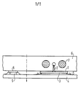
- the LSI module 3 designed as a micropack, is soldered to the pads of the printed circuit board using a flat spider.
- the cooling plate 6 on the rear sides of the building blocks 3 contains cooling passages through which coolant flows. Between the rear side of the building block and the cooling plate 6 there is also a metal plate 1, which is used for height compensation if other smaller building blocks, e.g. MSI's in conventional form with spacers 9 are also mounted on the circuit board 7.
- a suction channel 2 is provided for each micropack in the cooling plate 6 and through the cooling plate 1.
Abstract
Description
Die Erfindung betrifft eine Einrichtung zum Kühlen von Zu Flachbaugruppen zusammengefaßten gehäuselosen filmmontierten integrierten Bausteinen (Mikropacks), deren Außenanschlüsse (Outerleads) mit den zugehörigen Lötflecken (Pads) einer Leiterplatte verbunden sind, wobei die Rückenflächen mit einer allen Bausteinen gemeinsamen ebenen mit Kühlkanälen zur Aufnahme eines Kühlmediums versehenen Kühlplatte kontaktiert sind.The invention relates to a device for cooling housing-less film-mounted integrated components (micropacks) combined into flat assemblies, the outer connections (outer leads) of which are connected to the associated soldering pads (pads) of a printed circuit board, the back surfaces having a common plane with cooling channels for receiving a cooling component Cooling medium provided cooling plate are contacted.
Aus der europäischen Patentschrift 0 103 068 B1 ist eine Einrichtung zum Kühlen einer Mehrzahl von Zu Flachbaugruppen zusammengefaßten integrierten Bausteinen bekannt, bei der hochintegrierte Bausteine über einen Z-förmigen Spider mit der Leiterplatte verbunden sind. Dabei wird der Bauteilekörper auf den Spider aufgelötet (Innerleadbonding) und dann wird der Spider freigeschnitten und Z-förmig gebogen. Der so entstandene Mikropack wird mit den Außenanschlüssen (Outerleads) auf die Leiterplatte aufgelötet. Zwischen Baustein und Leiterplatte sitzen Druckstücke, die Toleranzunterschiede ausgleichen und den Andruck des Bausteins an die Kühlplatte gewährleisten, um die Verlustleistung abzuführen. Per Spider ist in Z-Richtung gebogen und muß Wegunterschiede in Z-Richtung ausgleichen, die durch Zusammendrücken des Druckstückes und durch die Biegung der Leiterplatte entstehen. Dies kann zu höheren Ungenauigkeiten am Spider führen.From European patent specification 0 103 068 B1, a device for cooling a plurality of integrated modules combined into flat modules is known, in which highly integrated modules are connected to the printed circuit board via a Z-shaped spider. The component body is soldered onto the spider (inner lead bonding) and then the spider is cut free and bent into a Z-shape. The resulting micropack is soldered onto the circuit board with the outer connections (outer leads). Pressure pieces sit between the module and the printed circuit board, which compensate for differences in tolerance and ensure that the module is pressed against the cooling plate in order to dissipate the power loss. The spider is bent in the Z direction and must compensate for path differences in the Z direction, which result from the compression of the pressure piece and the bending of the printed circuit board. This can lead to higher inaccuracies on the spider.
Aufgabe der vorliegenden Erfindung ist es, eine Einrichtung zum Kühlen von zu Flachbaugruppen Zusammengefaßten integrierten Bausteinen zu schaffen, die eine vereinfachte Herstellung von Mikropacks sowie eine vereinfachte Montage derselben auf Leiterplatten ermöglicht.The object of the present invention is to provide a device for cooling integrated modules which are combined to form flat assemblies, which enables simplified manufacture of micropacks and simplified assembly of the same on printed circuit boards.
Zur Lösung dieser Aufgabe wird die Einrichtung zum Kühlen von zu Flachbaugruppen Zusammengefaßten gehäuselosen Baustelnen derart ausgebildet, daß Zwischen Baustein und Kühlplatte ein mit einer an den Rändern verdichteten Metallfolie beschichtetes Metallplättchen liegt, daß in der Kühlplatte und durch das Kühlplättchen hindurch ein Absaugkanal vorgesehen ist, über den der Baustein durch Erzeugung eines Unterdrucks auf das Metallplättchen angedrückt wird und daß der Baustein einen flachen Spider aufweist, der mit entsprechenden Lötflecken auf der Leiterplatte kontaktiert ist.To solve this problem, the device for cooling housing assemblies combined into flat assemblies is designed such that between the block and the cooling plate there is a metal plate coated with a metal foil compressed at the edges, that a suction channel is provided in the cooling plate and through the cooling plate which the block is pressed onto the metal plate by generating a vacuum and that the block has a flat spider which is in contact with corresponding solder spots on the circuit board.
Durch diese Maßnahmen werden die durch den Biegevorgang des Spiders bei herkömmlichen Mikropacks häufig auftretenden Ungenauigkeiten zwischen der Deckungsgleichheit seiner Außenanschlüsse mit den jeweils zugeordneten Pads der Leiterplatte, die nur durch aufwendige zusätzliche Maßnahmen verhindert werden können, vermieden.These measures prevent the inaccuracies that often occur due to the bending process of the spider in conventional micropacks between the congruence of its external connections with the respectively assigned pads of the printed circuit board, which can only be prevented by complex additional measures.
Zum Temperaturausgleich zwischen Kühlplatte und Baustein können die Außenanschlüsse des Bausteins entweder mit einer Sicke in Z-Richtung versehen sein, oder mit Auslenkungen in der XY-Ebene.For temperature compensation between the cooling plate and the module, the external connections of the module can either be provided with a bead in the Z direction or with deflections in the XY plane.
Anhand des Ausführungsbeispiels nach der Figur wird die Erfindung näher erläutert.The invention is explained in more detail using the exemplary embodiment according to the figure.
Der als Mikropack ausgeführte LSI-Baustein 3 wird mit flachem Spider mit den Pads der Leiterplatte verlötet. Die Kühlplatte 6 an den Rückseiten der Bausteine 3 enthält kühlmitteldurchflossene Kühlkanäle 7. Zwischen der Bausteinrückseite und der Kühlplatte 6 liegt außerdem ein Metallplättchen 1, das zum Höhenausgleich dient, wenn weitere kleinere Bausteine, z.B. MSI's in herkömmlicher Form mit Zwischenstücken 9 ebenfalls auf der Leiterplatte 7 montiert sind. In der Kühlplatte 6 und durch das Kühlplättchen 1 hindurch ist für jeden Mikropack ein Absaugkanal 2 vorgesehen. Durch Erzeugen eines Unterdrucks wird der zwischen Kühlplatte und Leiterplatte 7 montierte Baustein 3 an das mit Metallfolie beschichtete Metallplättchen 1 angesaugt und somit ein guter Wärmekontakt hergestellt. Die Metallfolie 1 muß an den Rändern etwas dicker aufgebracht werden, um mit den Bausteinrand abzudichten.The LSI module 3, designed as a micropack, is soldered to the pads of the printed circuit board using a flat spider. The cooling plate 6 on the rear sides of the building blocks 3 contains cooling passages through which coolant flows. Between the rear side of the building block and the cooling plate 6 there is also a metal plate 1, which is used for height compensation if other smaller building blocks, e.g. MSI's in conventional form with spacers 9 are also mounted on the circuit board 7. A suction channel 2 is provided for each micropack in the cooling plate 6 and through the cooling plate 1. By generating a negative pressure, the component 3 mounted between the cooling plate and the printed circuit board 7 is sucked onto the metal plate 1 coated with metal foil, and thus good thermal contact is established. The metal foil 1 must be applied a little thicker at the edges in order to seal with the edge of the block.
Claims (3)
Applications Claiming Priority (2)
| Application Number | Priority Date | Filing Date | Title |
|---|---|---|---|
| DE4210835A DE4210835C1 (en) | 1992-04-01 | 1992-04-01 | |
| DE4210835 | 1992-04-01 |
Publications (1)
| Publication Number | Publication Date |
|---|---|
| EP0563679A1 true EP0563679A1 (en) | 1993-10-06 |
Family
ID=6455727
Family Applications (1)
| Application Number | Title | Priority Date | Filing Date |
|---|---|---|---|
| EP93104262A Ceased EP0563679A1 (en) | 1992-04-01 | 1993-03-16 | Cooling device for bare integrated components assembled as a flat structure |
Country Status (2)
| Country | Link |
|---|---|
| EP (1) | EP0563679A1 (en) |
| DE (1) | DE4210835C1 (en) |
Cited By (1)
| Publication number | Priority date | Publication date | Assignee | Title |
|---|---|---|---|---|
| GB2392010A (en) * | 2002-06-18 | 2004-02-18 | Bosch Gmbh Robert | Semiconductor module cooling device |
Citations (1)
| Publication number | Priority date | Publication date | Assignee | Title |
|---|---|---|---|---|
| US4758926A (en) * | 1986-03-31 | 1988-07-19 | Microelectronics And Computer Technology Corporation | Fluid-cooled integrated circuit package |
Family Cites Families (5)
| Publication number | Priority date | Publication date | Assignee | Title |
|---|---|---|---|---|
| JPS5772357A (en) * | 1980-10-24 | 1982-05-06 | Nec Corp | Mounting method of integrated circuit |
| ATE39788T1 (en) * | 1982-09-09 | 1989-01-15 | Siemens Ag | DEVICE FOR COOLING A NUMBER OF INTEGRATED COMPONENTS COMBINED TO FORM FLAT ASSEMBLIES. |
| JPS62238653A (en) * | 1986-04-09 | 1987-10-19 | Nec Corp | Cooling structure |
| EP0357747A1 (en) * | 1988-03-01 | 1990-03-14 | Digital Equipment Corporation | Method and apparatus for packaging and cooling integrated circuit chips |
| US4884630A (en) * | 1988-07-14 | 1989-12-05 | Microelectronics And Computer Technology Corporation | End fed liquid heat exchanger for an electronic component |
-
1992
- 1992-04-01 DE DE4210835A patent/DE4210835C1/de not_active Expired - Fee Related
-
1993
- 1993-03-16 EP EP93104262A patent/EP0563679A1/en not_active Ceased
Patent Citations (1)
| Publication number | Priority date | Publication date | Assignee | Title |
|---|---|---|---|---|
| US4758926A (en) * | 1986-03-31 | 1988-07-19 | Microelectronics And Computer Technology Corporation | Fluid-cooled integrated circuit package |
Non-Patent Citations (1)
| Title |
|---|
| PATENT ABSTRACTS OF JAPAN vol. 014, no. 558 (P-1141)12. Dezember 1990 & JP-A-02 238 380 ( FUJITSU LTD ) 20. September 1990 * |
Cited By (3)
| Publication number | Priority date | Publication date | Assignee | Title |
|---|---|---|---|---|
| GB2392010A (en) * | 2002-06-18 | 2004-02-18 | Bosch Gmbh Robert | Semiconductor module cooling device |
| US6822865B2 (en) | 2002-06-18 | 2004-11-23 | Robert Bosch Gmbh | Cooling device for semiconductor modules |
| GB2392010B (en) * | 2002-06-18 | 2005-04-13 | Bosch Gmbh Robert | Cooling device for semiconductor modules |
Also Published As
| Publication number | Publication date |
|---|---|
| DE4210835C1 (en) | 1993-06-17 |
Similar Documents
| Publication | Publication Date | Title |
|---|---|---|
| EP0931346B1 (en) | Microelectronic component with a sandwich design | |
| DE10213648A1 (en) | The power semiconductor module | |
| DE4220966C2 (en) | Method for producing a carrier plate for electrical components | |
| CH667562A5 (en) | PROCEDURE FOR MODIFYING A FLAT ELECTRICAL ASSEMBLY. | |
| DE4015788A1 (en) | ASSEMBLY | |
| DE19924993C2 (en) | Intelligent power module in sandwich construction | |
| EP0494153B1 (en) | Compound arrangement with printed circuit board | |
| DE2843710B2 (en) | Multi-layer flexible printed circuit board and method for making same | |
| DE3627372C2 (en) | ||
| EP1508168A1 (en) | Semiconductor component | |
| DE19942770A1 (en) | Power semiconductor module | |
| EP0563679A1 (en) | Cooling device for bare integrated components assembled as a flat structure | |
| WO1996013966A1 (en) | Current supply module for mounting on a component-carrying printed circuit board | |
| EP0153990B1 (en) | Flat module | |
| EP0312528B1 (en) | Multiple-plate hybrid device | |
| DE3323246A1 (en) | Power semiconductor module | |
| DE2904012A1 (en) | Support rack for protective retention of printed circuit boards - has board retaining capsules with terminal blocks and external terminals for connecting outer lines | |
| DE3813566A1 (en) | Electrical connection between a hybrid assembly and a printed circuit board, and a method for its production | |
| DE4210834A1 (en) | Heat sink for integrated circuit micro-chip thin film package - uses cooling plate with cooling channels open to membrane sealed to underside of plate inside facing IC micro-package | |
| DE2703889A1 (en) | Housing for electric power components - has circuit board with edge teeth engaging teeth in U=shaped frame and heat-sink cover | |
| DE10249206B3 (en) | Method of assembling a power device | |
| EP0751569A2 (en) | Hybrid power circuit | |
| DE19511486A1 (en) | Mfr. of laminated circuit boards e.g. for control units in motor vehicle engineering | |
| DE4217596C2 (en) | Installation system for highly integrated components mounted on printed circuit boards | |
| EP0379624A1 (en) | Arrangement of a semiconductor component suited for surface mounting and process for mounting it on a circuit board |
Legal Events
| Date | Code | Title | Description |
|---|---|---|---|
| PUAI | Public reference made under article 153(3) epc to a published international application that has entered the european phase |
Free format text: ORIGINAL CODE: 0009012 |
|
| AK | Designated contracting states |
Kind code of ref document: A1 Designated state(s): AT BE CH DE FR GB IT LI NL |
|
| 17P | Request for examination filed |
Effective date: 19931020 |
|
| 17Q | First examination report despatched |
Effective date: 19950316 |
|
| STAA | Information on the status of an ep patent application or granted ep patent |
Free format text: STATUS: THE APPLICATION HAS BEEN REFUSED |
|
| 18R | Application refused |
Effective date: 19950727 |