EP0532169A1 - Optical Inspection Probe - Google Patents
Optical Inspection Probe Download PDFInfo
- Publication number
- EP0532169A1 EP0532169A1 EP92307017A EP92307017A EP0532169A1 EP 0532169 A1 EP0532169 A1 EP 0532169A1 EP 92307017 A EP92307017 A EP 92307017A EP 92307017 A EP92307017 A EP 92307017A EP 0532169 A1 EP0532169 A1 EP 0532169A1
- Authority
- EP
- European Patent Office
- Prior art keywords
- array
- time
- probe
- image
- feature
- Prior art date
- Legal status (The legal status is an assumption and is not a legal conclusion. Google has not performed a legal analysis and makes no representation as to the accuracy of the status listed.)
- Granted
Links
Images


Classifications
-
- G—PHYSICS
- G01—MEASURING; TESTING
- G01B—MEASURING LENGTH, THICKNESS OR SIMILAR LINEAR DIMENSIONS; MEASURING ANGLES; MEASURING AREAS; MEASURING IRREGULARITIES OF SURFACES OR CONTOURS
- G01B11/00—Measuring arrangements characterised by the use of optical techniques
- G01B11/02—Measuring arrangements characterised by the use of optical techniques for measuring length, width or thickness
- G01B11/024—Measuring arrangements characterised by the use of optical techniques for measuring length, width or thickness by means of diode-array scanning
-
- G—PHYSICS
- G01—MEASURING; TESTING
- G01B—MEASURING LENGTH, THICKNESS OR SIMILAR LINEAR DIMENSIONS; MEASURING ANGLES; MEASURING AREAS; MEASURING IRREGULARITIES OF SURFACES OR CONTOURS
- G01B11/00—Measuring arrangements characterised by the use of optical techniques
Definitions
- the present invention relates to an optical probe which in use is mounted on the movable arm of a coordinate positioning machine to enable the machine to determine the position of a surface. More particularly, the invention relates to a non-contact probe which, upon detection of a surface, emits a trigger signal which is sent to the machine control to cause it to record the position of the movable arm at the instant of trigger, thereby to determine the position of the surface.
- a non-contact trigger probe in the form of a video camera which projects an image of a workpiece to be measured onto a charge-coupled device (CCD) array.
- the CCD array consists of a large number of pixels each of which outputs an electrical signal corresponding to the intensity of light incident thereon.
- the known video trigger probe emits a trigger signal indicating detection of the edge of a surface when the value of the output signal of a predesignated pixel passes above or below a threshold level.
- the problem with such a known probe is that the image processing circuitry in the probe sequentially scans each pixel in the CCD array; the time period for a single scan of the entire array being of the order of 20ms. There is therefore a possible time band of 20ms during which the output of the predesignated pixel may have passed the threshold level.
- the accuracy of a measurement made with this known probe is therefore limited to the speed at which the image processing circuitry may scan the entire CCD array.
- the present invention seeks to ameliorate this problem by detecting the position of a feature on a surface using a video probe which focuses an image of the workpiece onto an array (e.g. a charge-coupled transistor (CCT) or a CCD array), and which determines the position of the feature by anticipating the instant of time at which the image of the said feature passes across a predesignated pixel in the array, in order to emit a trigger signal at the said instant of time.
- an array e.g. a charge-coupled transistor (CCT) or a CCD array
- the present invention provides an optical inspection probe for use on a movable arm of a coordinate positioning machine to determine the position of a feature of a surface, the probe comprising: a sensing device having a light sensitive array which includes a plurality of discrete light sensitive cells, each of which outputs a signal corresponding to the intensity of light incident thereon; an imaging device having one or more optical components for imaging said feature on said array; and processing means for
- the present invention is applicable to detection in which the probe detects e.g. the edge of a surface by moving substantially parallel to the surface, or in which the height of the surface is determined by moving the probe substantially perpendicular to the surface.
- the feature is provided by a light pattern (such as a spot) on the surface generated by a light beam which extends at an angle to the optical axis of the probe; the position of incidence of the pattern on the surface moves laterally with respect to the optical axis as the probe approaches the surface substantially in a direction along said axis.
- the speed and relative direction of travel of the probe and workpiece will be determined using the image processing circuitry of the probe for example, by determining from consecutive image frames of the array the relative displacement of the probe and surface; this obviates the need to provide any inputs to the probe from the machine control.
- the speed and relative direction of travel of the probe and workpiece may be input into the probe from the machine control
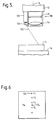
- a video probe 10 is supported on the quill 12 of a coordinate measuring machine, and is thereby movable in three directions X,Y,Z relative to a table 14 of the machine.
- a machine control (not shown) controls movement of the quill 12 (and thus the probe 10) relative to the table; coordinate measuring machines are well known per se and will not be described further.
- the probe 10 comprises an optical imaging device in the form of an imaging module 16 for imaging e.g. a feature of a workpiece surface W onto an array 18 (which may be a CCT or a CCD array) provided within the probe 10.
- the imaging module 16 is in this case a convex lens, however other and more complex modules may be employed in accordance with the required measuring operation.
- the CCD array 18 is provided in a sensing module to which an imaging module may be releasably connectable in the manner described in EP 501710A.
- the array 18 comprises a plurality of pixels 20 each of which generates a electrical signal in dependence upon the intensity of light incident thereon.
- the data from each pixel is acquired by the image processing circuitry (not shown) of the probe by sequentially scanning each row r1,r2..r n of the CCD array 18.
- the scanning of the CCD array 18 generates a signal having a synchronising pulse p s followed by a data stream comprising an individual analogue signal for each pixel Q n in the row r n .
- Each of the analogue signals Q n (corresponding to a light intensity) is typically converted to an 8-bit digital signal, which may thus have one of 28 values.
- the image processing circuitry of the video probe determines from the value of each 8-bit number whether the light intensity incident upon each pixel is such as to represent an image of the surface of the workpiece (i.e. if the value of the 8-bit number exceeds a predetermined value then the light intensity incident upon a given pixel is deemed to have been reflected off the surface to be detected).
- Such processing circuitry is well known per se .
- a feature of a surface in this case an edge
- the image of the surface S of the workpiece W is focused upon the CCD array 18. It is desired to determine the instant of time at which the image of the edge of the surface S will pass across the centre pixel Q c .
- This instant will correspond to a predetermined threshold value of, for example: the value of the 8-bit number representing the light intensity incident upon Q c ; a predetermined magnitude of change in the value of the 8-bit number from one scan of the array 18 to the next; or a predetermined rate of change in the value of the 8-bit number.
- Fig 4a is an illustration of the probing operation at a time t1 at which the distance between the surface S and the centre pixel Q c (in the direction of relative motion of the surface S and probe 10) is h1.
- Fig 4b illustrates the situation at a time t2, the time interval t2 - t1 being equal to a single scanning period T for the CCD array 18.
- the distance between the surface S and the centre pixel Q c is now h2.
- x h2 - h1
- v x/T
- Fig 4c is an image frame at time t n , the time interval t n - t2 once again being equal to (n-2) multiples of the scanning period T of the CCD array 18. It can be seen from Fig 4c and 4d that during the time interval t n +1 - t n , the image of the edge of the surface S has passed completely over the centre pixel Q c , and that the centre pixel Q c now lies some distance beyond the image of the edge of the surface S.
- h2 (n-2) x + e
- x is the distance of relative travel between the probe and surface over a single scanning period T
- e is the distance of relative travel between the probe and surface over the time interval ⁇ t.
- the image processing circuitry of the probe 10 should therefore output a trigger signal at a time interval (n-2)T+ ⁇ t after time t2, which is then accurately indicative of the instant of time at which the edge of the surface S passes over the centre pixel Q c .
- the time required to calculate the value of [(n-2)T+ ⁇ t] is dependent upon factors such as the direction of relative movement of the surface and the array, and is therefore variable.
- the value of m should therefore ideally be determined on each occasion.
- the determination of the instant of trigger is performed (n-2) frames in advance of the "event frame” to allow sufficient time (a) for performing the processing to determine the value of [(n-2)T+ ⁇ t), and (b) to correct for the processing time required: i.e. to generate the value of [(n-m-2)T+ ⁇ t).
- the velocity vector representing the relative velocity between the surface S and the probe 10 may be input directly into the image processing circuitry from the machine control.
- the first embodiment of the present invention related to a non-contact trigger probe whose purpose was, for example, to determine the position of the edge of a surface when travelling laterally with respect to the plane of the surface.
- a second embodiment of the present invention provides a non-contact trigger probe for determining the position of a predetermined height above a plane surface.
- a probe 100 is supported on the movable arm or quill 12 of a coordinate positioning machine for movement in the x,y,z directions relative to a table 14.
- the probe 100 comprises an imaging module having one or more optical imaging components such as a lens 116, and an array 118 (e.g. a CCD array) onto which an image is focused.
- the probe comprises a light source, typically a laser 120 (an LED or other source may be used) which emits a beam 122 of light.
- the beam 122 is projected at an angle relative to the axis A of the probe 100, and in this example this is achieved by passing the beam 122 through a prism 124.
- the beam 122 is incident upon a surface S, and consequently illuminates the surface S with a spot 126.
- the angle of deviation of the beam 122 relative to the axis of the probe 100 is such that when an image of the spot 126 on the CCD array 118 passes across the centre pixel Q c of the array 118, the quill 12 is at a height above the surface S at which is desired to produce a trigger signal.
- the spot 126 provided by the light beam 122 is thus the "feature" to be inspected.
- Fig 6 shows the position of the image of the spot 126 on the CCD array 118 at time t1,t2,t3, and t4, each of which correspond to instants at which a scanning operation of the CCD array 118 has been completed. It can be seen from the Fig 6 that the incident of time t e at which the image of the spot 126 passes across the centre pixel Q c occurs after time t3, but before time t4. Therefore, in order to output a trigger signal at the correct instant of time t e , the anticipation technique described in relation to the first embodiment of the present invention is employed here.
Abstract
Description
- The present invention relates to an optical probe which in use is mounted on the movable arm of a coordinate positioning machine to enable the machine to determine the position of a surface. More particularly, the invention relates to a non-contact probe which, upon detection of a surface, emits a trigger signal which is sent to the machine control to cause it to record the position of the movable arm at the instant of trigger, thereby to determine the position of the surface.
- It is known to provide a non-contact trigger probe in the form of a video camera which projects an image of a workpiece to be measured onto a charge-coupled device (CCD) array. The CCD array consists of a large number of pixels each of which outputs an electrical signal corresponding to the intensity of light incident thereon. The known video trigger probe emits a trigger signal indicating detection of the edge of a surface when the value of the output signal of a predesignated pixel passes above or below a threshold level. The problem with such a known probe is that the image processing circuitry in the probe sequentially scans each pixel in the CCD array; the time period for a single scan of the entire array being of the order of 20ms. There is therefore a possible time band of 20ms during which the output of the predesignated pixel may have passed the threshold level. The accuracy of a measurement made with this known probe is therefore limited to the speed at which the image processing circuitry may scan the entire CCD array.
- The present invention, seeks to ameliorate this problem by detecting the position of a feature on a surface using a video probe which focuses an image of the workpiece onto an array (e.g. a charge-coupled transistor (CCT) or a CCD array), and which determines the position of the feature by anticipating the instant of time at which the image of the said feature passes across a predesignated pixel in the array, in order to emit a trigger signal at the said instant of time.
- Accordingly the present invention provides an optical inspection probe for use on a movable arm of a coordinate positioning machine to determine the position of a feature of a surface, the probe comprising:
a sensing device having a light sensitive array which includes a plurality of discrete light sensitive cells, each of which outputs a signal corresponding to the intensity of light incident thereon;
an imaging device having one or more optical components for imaging said feature on said array; and
processing means for - a) analysing said image by, inter alia, sequentially scanning each cell of said array to determine the value of each said signal, a single scan of said array constituting an image frame; and
- b) determining in advance, from two or more said image frames, the instant of time at which the image of said feature will reach a predetermined cell of said array, and for generating at said instant a trigger signal for instructing the machine control system to determine the position of the movable arm.
- The present invention is applicable to detection in which the probe detects e.g. the edge of a surface by moving substantially parallel to the surface, or in which the height of the surface is determined by moving the probe substantially perpendicular to the surface. Where the height of the surface is determined, the feature is provided by a light pattern (such as a spot) on the surface generated by a light beam which extends at an angle to the optical axis of the probe; the position of incidence of the pattern on the surface moves laterally with respect to the optical axis as the probe approaches the surface substantially in a direction along said axis.
- Preferably, the speed and relative direction of travel of the probe and workpiece will be determined using the image processing circuitry of the probe for example, by determining from consecutive image frames of the array the relative displacement of the probe and surface; this obviates the need to provide any inputs to the probe from the machine control. Alternatively however, the speed and relative direction of travel of the probe and workpiece may be input into the probe from the machine control
- Embodiments of the present invention will now be described, by way of example, and with reference to the accompanying drawings in which:
- Fig 1 shows a first type of video camera mounted to a coordinate measuring machine;
- Fig 2 shows a representation of a CCD array in the probe of Fig 1;
- Fig 3 is a signal diagram showing the output of a row of pixels in the CCD array of Fig 1; and
- Figs 4a-d illustrate a probing operation according to a first embodiment of the present invention;
- Fig 5 shows a second type of video camera mounted to a coordinate measuring machine; and
- Fig 6 illustrates a probing operation according to a second embodiment of the present invention.
- Referring now to Fig 1, a
video probe 10 is supported on thequill 12 of a coordinate measuring machine, and is thereby movable in three directions X,Y,Z relative to a table 14 of the machine. A machine control (not shown) controls movement of the quill 12 (and thus the probe 10) relative to the table; coordinate measuring machines are well known per se and will not be described further. Theprobe 10 comprises an optical imaging device in the form of animaging module 16 for imaging e.g. a feature of a workpiece surface W onto an array 18 (which may be a CCT or a CCD array) provided within theprobe 10. Theimaging module 16 is in this case a convex lens, however other and more complex modules may be employed in accordance with the required measuring operation. - Referring now to Fig 2, the
CCD array 18 is provided in a sensing module to which an imaging module may be releasably connectable in the manner described in EP 501710A. Thearray 18 comprises a plurality of pixels 20 each of which generates a electrical signal in dependence upon the intensity of light incident thereon. The data from each pixel (in the form of the aforementioned electrical signals) is acquired by the image processing circuitry (not shown) of the probe by sequentially scanning each row r₁,r₂..rn of theCCD array 18. - Referring now to Fig 3, the scanning of the
CCD array 18 generates a signal having a synchronising pulse ps followed by a data stream comprising an individual analogue signal for each pixel Qn in the row rn. Each of the analogue signals Qn (corresponding to a light intensity) is typically converted to an 8-bit digital signal, which may thus have one of 2⁸ values. The image processing circuitry of the video probe then determines from the value of each 8-bit number whether the light intensity incident upon each pixel is such as to represent an image of the surface of the workpiece (i.e. if the value of the 8-bit number exceeds a predetermined value then the light intensity incident upon a given pixel is deemed to have been reflected off the surface to be detected). Such processing circuitry is well known per se. - Referring now to Figs 4a-D an operation in which a feature of a surface (in this case an edge) is inspected will now be described. In Fig 4a the image of the surface S of the workpiece W is focused upon the
CCD array 18. It is desired to determine the instant of time at which the image of the edge of the surface S will pass across the centre pixel Qc. This instant will correspond to a predetermined threshold value of, for example: the value of the 8-bit number representing the light intensity incident upon Qc; a predetermined magnitude of change in the value of the 8-bit number from one scan of thearray 18 to the next; or a predetermined rate of change in the value of the 8-bit number. Fig 4a is an illustration of the probing operation at a time t₁ at which the distance between the surface S and the centre pixel Qc (in the direction of relative motion of the surface S and probe 10) is h₁. Fig 4b illustrates the situation at a time t₂, the time interval t₂ - t₁ being equal to a single scanning period T for theCCD array 18. The distance between the surface S and the centre pixel Qc is now h₂. From the image frames represented in Figs 4a and 4b, the image processing circuitry may determine, the distances h₁, and h₂, and thus the distance (x) and direction of relative travel of the probe and the surface S over the time interval t₂-t₁ (=T). By using this information in a best fit operation the relative velocity of the probe and the surface S may be determined.
- Fig 4c is an image frame at time tn, the time interval tn - t₂ once again being equal to (n-2) multiples of the scanning period T of the
CCD array 18. It can be seen from Fig 4c and 4d that during the time interval tn+₁ - tn, the image of the edge of the surface S has passed completely over the centre pixel Qc, and that the centre pixel Qc now lies some distance beyond the image of the edge of the surface S. - Clearly, the instant of time at which the edge of the surface S passed over the centre pixel Qc is at a time te, which lies between the times tn and tn+₁, where:

- Now at time t₂ the distance from the edge of the surface S to the centre pixel Qc is h₂. This distance h₂ may be expressed in the following way:

where:
x is the distance of relative travel between the probe and surface over a single scanning period T;
e is the distance of relative travel between the probe and surface over the time interval Δt. - Since h₂, (n-2) and x are known, e may be calculated.
- Assuming the velocity v remains constant:

- The image processing circuitry of the
probe 10 should therefore output a trigger signal at a time interval (n-2)T+Δt after time t₂, which is then accurately indicative of the instant of time at which the edge of the surface S passes over the centre pixel Qc. - However, the image processing required to perform this calculation takes a significant amount of time in relation to the magnitude of the time interval [(n-2)T+Δt]. As a result, by the time the value of [(n-2)T+Δt] has been calculated, a number (m) of further scans of the
array 18 have been completed. The value of [(n-2)T+Δt] is therefore not generated until time t2+m, by which time the interval te to the event has been has been reduced by mT, and is therefore equal to:
- The time required to calculate the value of [(n-2)T+Δt] is dependent upon factors such as the direction of relative movement of the surface and the array, and is therefore variable. The value of m should therefore ideally be determined on each occasion.
- The determination of the instant of trigger is performed (n-2) frames in advance of the "event frame" to allow sufficient time (a) for performing the processing to determine the value of [(n-2)T+Δt), and (b) to correct for the processing time required: i.e. to generate the value of [(n-m-2)T+Δt).
- However the calculation of [(n-m-2)T+Δt) must assume a constant velocity in order to be performed in advance. Any variation in velocity after time t₂ will therefore be a source of error. This may be minimised by performing a calculation after each frame (i.e. at times t₁, t₂, t₃...etc), and using only the value of [(n-m-2)T+Δt] obtained from the processing sequence at which it is determined that insufficient time remains before the instant te to generate any further value of [(n-m-2)T+Δt) and output the trigger signal at the correct time.
- In a modification of the present invention, the velocity vector representing the relative velocity between the surface S and the
probe 10 may be input directly into the image processing circuitry from the machine control. - However, it is desirable to operate the probe exactly as a conventional touch-trigger probe so that the video probe is functionally interchangeable therewith. It is therefore preferable to avoid this if possible.
- The first embodiment of the present invention related to a non-contact trigger probe whose purpose was, for example, to determine the position of the edge of a surface when travelling laterally with respect to the plane of the surface. A second embodiment of the present invention provides a non-contact trigger probe for determining the position of a predetermined height above a plane surface.
- Referring now to Fig 5, a
probe 100 is supported on the movable arm or quill 12 of a coordinate positioning machine for movement in the x,y,z directions relative to a table 14. As with the first embodiment, theprobe 100 comprises an imaging module having one or more optical imaging components such as alens 116, and an array 118 (e.g. a CCD array) onto which an image is focused. Additionally, the probe comprises a light source, typically a laser 120 (an LED or other source may be used) which emits abeam 122 of light. Thebeam 122 is projected at an angle relative to the axis A of theprobe 100, and in this example this is achieved by passing thebeam 122 through aprism 124. Thebeam 122 is incident upon a surface S, and consequently illuminates the surface S with aspot 126. The angle of deviation of thebeam 122 relative to the axis of theprobe 100 is such that when an image of thespot 126 on theCCD array 118 passes across the centre pixel Qc of thearray 118, thequill 12 is at a height above the surface S at which is desired to produce a trigger signal. Thespot 126 provided by thelight beam 122 is thus the "feature" to be inspected. - Fig 6 shows the position of the image of the
spot 126 on theCCD array 118 at time t₁,t₂,t₃, and t₄, each of which correspond to instants at which a scanning operation of theCCD array 118 has been completed. It can be seen from the Fig 6 that the incident of time te at which the image of thespot 126 passes across the centre pixel Qc occurs after time t₃, but before time t₄. Therefore, in order to output a trigger signal at the correct instant of time te, the anticipation technique described in relation to the first embodiment of the present invention is employed here. - The processing method by which a trigger signal is output at time te is exactly as described in relation to the first embodiment of the present invention and will not be described further.
Claims (7)
- An optical inspection probe (10) for use on a movable arm (12) of a coordinate positioning machine to determine the position of a feature of a surface (S), the probe (10) comprising:
a sensing device having a light sensitive array (18) which includes a plurality of discrete light sensitive cells (Q), each of which outputs a signal corresponding to the intensity of light incident thereon;
an imaging device (16) having one or more optical components for imaging said feature on said array;
characterised by:
processing means fora) analysing said image by, inter alia, sequentially scanning each cell (Q) of said array (18) to determine the value of each said signal, a single scan of said array (18) constituting an image frame; andb) determining in advance, from two or more said image frames, the instant of time (te) at which the image of said feature will reach a predetermined cell (Qc) of said array, and for generating at said instant a trigger signal for instructing the machine control system to determine the position of the movable arm (12). - An optical inspection probe according to claim 1 wherein the processing means includes means for determining, from at least two of said image frames, the speed and direction of relative travel of the probe (10) and the surface (S), and calculating from said parameters the time interval ([(n-2)T+Δt]) between the second of said image frames and said instant of time (te).
- An optical inspection probe according to claim 1 or claim 2 wherein the processing means includes means for determining the processing time (mT) required to calculate said time interval ([(n-2)T+Δt]), and for comparing said time interval ([(n-2)T+Δt]) with said processing time (mT) in order to determine whether a further calculation of said time interval ([(n-2)T+Δt]) may be made before said instant of time (te), and where sufficient time remains, performing a further calculation of said time interval ([(n-2)T+Δt]).
- An optical inspection probe according to claim 3, wherein said processing means includes means for generating a corrected value ([(n-2)T+Δt]-mT) of said time interval ([(n-2)T+Δt]) by subtracting the processing time (mT) therefrom.
- An optical inspection probe according to claim 1, wherein the probe (100) has an optical axis (A) extending orthogonal to said array (118) and illuminating means (120,124) for generating a light beam (122) to illuminate an area of said surface, wherein said light beam (122) extends at an angle to the optical axis (A).
- An optical inspection probe according to claim 1, wherein said sensing device (18) and said imaging device (16) are provided in the form of a sensing module and an imaging module and means are provided for releasably and repeatably retaining said imaging module on said sensing module.
- A method of inspecting a surface to determine the position of a feature thereon, using a coordinate positioning machine having an optical inspection probe connected to a movable arm of the machine, the optical inspection probe including a sensing module having an array of light sensitive elements each of which outputs a signal corresponding to the intensity of light incident thereon, and one or more optical elements for imaging said feature on said array, the method comprising the steps of:
analysing said image by, inter alia, sequentially scanning each light sensitive element of said array to determine the value of each said signal, a single scan of said array constituting an image frame;
determining, in advance, from two or more said image frames, the instant of time at which the image of said feature will reach a predetermined cell of said array, and generating at said instant a trigger signal for instructing the machine control system to determine the position of the movable arm.
Applications Claiming Priority (2)
| Application Number | Priority Date | Filing Date | Title |
|---|---|---|---|
| GB919117974A GB9117974D0 (en) | 1991-08-20 | 1991-08-20 | Non-contact trigger probe |
| GB9117974 | 1991-08-20 |
Publications (2)
| Publication Number | Publication Date |
|---|---|
| EP0532169A1 true EP0532169A1 (en) | 1993-03-17 |
| EP0532169B1 EP0532169B1 (en) | 1996-03-13 |
Family
ID=10700258
Family Applications (1)
| Application Number | Title | Priority Date | Filing Date |
|---|---|---|---|
| EP92307017A Expired - Lifetime EP0532169B1 (en) | 1991-08-20 | 1992-07-31 | Optical Inspection Probe |
Country Status (5)
| Country | Link |
|---|---|
| US (1) | US5319442A (en) |
| EP (1) | EP0532169B1 (en) |
| JP (1) | JPH05215518A (en) |
| DE (1) | DE69208982D1 (en) |
| GB (1) | GB9117974D0 (en) |
Cited By (10)
| Publication number | Priority date | Publication date | Assignee | Title |
|---|---|---|---|---|
| EP0837300A2 (en) * | 1996-10-21 | 1998-04-22 | Carl Zeiss | Procedure to measure the contours of objects |
| WO2000060307A1 (en) * | 1999-04-06 | 2000-10-12 | Renishaw Plc | Measuring probe with diaphragms and modules |
| DE10014627A1 (en) * | 2000-03-24 | 2001-09-27 | Sick Ag | Method and device for imaging objects |
| WO2002070211A1 (en) * | 2001-03-08 | 2002-09-12 | Carl Zeiss | Co-ordinate measuring device with a video probehead |
| WO2003009070A2 (en) * | 2001-07-16 | 2003-01-30 | Werth Messtechnik Gmbh | Method for measuring an object by means of a co-ordinate measuring device with an image processing sensor |
| WO2006102026A2 (en) | 2005-03-23 | 2006-09-28 | Microscan Systems Inc. | Focusing system using light source and image sensor |
| EP1729086A1 (en) * | 2005-06-03 | 2006-12-06 | Mitutoyo Corporation | Image measuring system, image measuring method and image measuring program |
| DE102019202798A1 (en) * | 2019-03-01 | 2020-09-03 | Pepperl + Fuchs Gmbh | Method and device for determining the relative speed between an object and a detector |
| DE102019202797A1 (en) * | 2019-03-01 | 2020-09-03 | Pepperl+Fuchs Gmbh | Method and device for determining the relative speed between an object and a detector |
| DE102019204824A1 (en) * | 2019-04-04 | 2020-10-08 | Pepperl + Fuchs Gmbh | Method and device for determining the relative speed between an object and a detector |
Families Citing this family (19)
| Publication number | Priority date | Publication date | Assignee | Title |
|---|---|---|---|---|
| US5450203A (en) * | 1993-12-22 | 1995-09-12 | Electroglas, Inc. | Method and apparatus for determining an objects position, topography and for imaging |
| US5825666A (en) * | 1995-06-07 | 1998-10-20 | Freifeld; Daniel | Optical coordinate measuring machines and optical touch probes |
| DE19642293C2 (en) * | 1996-10-14 | 1998-07-16 | Zeiss Carl Jena Gmbh | Coordinate measuring device |
| US5881780A (en) * | 1997-08-05 | 1999-03-16 | Dcl, Inc. | Apapratus for and method of locating the center of an opening in a vehicle |
| US5929459A (en) * | 1997-09-23 | 1999-07-27 | Synergistech, Inc. | Methods and apparatus for inspecting a workpiece with edge and co-planarity determination |
| US6094269A (en) * | 1997-12-31 | 2000-07-25 | Metroptic Technologies, Ltd. | Apparatus and method for optically measuring an object surface contour |
| WO2001090726A2 (en) * | 2000-05-19 | 2001-11-29 | Aclara Biosciences, Inc. | Optical alignment in capillary detection using capillary wall scatter |
| US6610992B1 (en) | 2000-07-19 | 2003-08-26 | Clasmet | Rotating beam method and system for measuring part edges and openings |
| US7881896B2 (en) | 2002-02-14 | 2011-02-01 | Faro Technologies, Inc. | Portable coordinate measurement machine with integrated line laser scanner |
| CN100376863C (en) * | 2004-12-17 | 2008-03-26 | 鸿富锦精密工业(深圳)有限公司 | Image measuring system and method for section difference of heat radiator |
| GB0707921D0 (en) * | 2007-04-24 | 2007-05-30 | Renishaw Plc | Apparatus and method for surface measurement |
| CA2597891A1 (en) * | 2007-08-20 | 2009-02-20 | Marc Miousset | Multi-beam optical probe and system for dimensional measurement |
| GB0809037D0 (en) | 2008-05-19 | 2008-06-25 | Renishaw Plc | Video Probe |
| JP5684712B2 (en) * | 2008-10-29 | 2015-03-18 | レニショウ パブリック リミテッド カンパニーRenishaw Public Limited Company | Method for coordinate measuring system |
| EP3184957B1 (en) * | 2015-12-23 | 2021-07-14 | Hexagon Technology Center GmbH | Modular micro optics for optical probes |
| US11268301B2 (en) | 2017-04-27 | 2022-03-08 | Reinhard Matye | Automatic hatch for bulk material containers |
| US11286123B2 (en) | 2019-06-20 | 2022-03-29 | Dcl, Inc. | Camera-enabled loader system and method |
| CN112336295A (en) * | 2019-08-08 | 2021-02-09 | 上海安翰医疗技术有限公司 | Method and device for controlling magnetic capsule endoscope, storage medium, and electronic device |
| CN114814266B (en) * | 2022-05-20 | 2023-04-14 | 中国工程物理研究院流体物理研究所 | Arc centripetal array speed measurement probe and speed measurement method |
Citations (1)
| Publication number | Priority date | Publication date | Assignee | Title |
|---|---|---|---|---|
| US4970653A (en) * | 1989-04-06 | 1990-11-13 | General Motors Corporation | Vision method of detecting lane boundaries and obstacles |
Family Cites Families (1)
| Publication number | Priority date | Publication date | Assignee | Title |
|---|---|---|---|---|
| JPS60194302A (en) * | 1984-03-14 | 1985-10-02 | Toshiba Corp | Measuring apparatus for object to be photographed |
-
1991
- 1991-08-20 GB GB919117974A patent/GB9117974D0/en active Pending
-
1992
- 1992-07-31 EP EP92307017A patent/EP0532169B1/en not_active Expired - Lifetime
- 1992-07-31 DE DE69208982T patent/DE69208982D1/en not_active Expired - Lifetime
- 1992-08-11 US US07/927,960 patent/US5319442A/en not_active Expired - Fee Related
- 1992-08-20 JP JP4221643A patent/JPH05215518A/en active Pending
Patent Citations (1)
| Publication number | Priority date | Publication date | Assignee | Title |
|---|---|---|---|---|
| US4970653A (en) * | 1989-04-06 | 1990-11-13 | General Motors Corporation | Vision method of detecting lane boundaries and obstacles |
Non-Patent Citations (1)
| Title |
|---|
| PATENT ABSTRACTS OF JAPAN vol. 10, no. 48 (P-431)(2105) 25 February 1986 & JP-A-60 194 302 ( TOSHIBA K.K. ) 2 October 1985 * |
Cited By (25)
| Publication number | Priority date | Publication date | Assignee | Title |
|---|---|---|---|---|
| EP0837300A3 (en) * | 1996-10-21 | 2001-03-21 | Carl Zeiss | Procedure to measure the contours of objects |
| EP0837300A2 (en) * | 1996-10-21 | 1998-04-22 | Carl Zeiss | Procedure to measure the contours of objects |
| US7146741B2 (en) | 1999-04-06 | 2006-12-12 | Renishaw Plc | Measuring probe with diaphragms and modules |
| WO2000060307A1 (en) * | 1999-04-06 | 2000-10-12 | Renishaw Plc | Measuring probe with diaphragms and modules |
| US6430833B1 (en) | 1999-04-06 | 2002-08-13 | Renishaw Plc | Measuring probe with diaphragms and modules |
| EP1505362A1 (en) * | 1999-04-06 | 2005-02-09 | Renishaw plc | Measuring probe with modules |
| DE10014627A1 (en) * | 2000-03-24 | 2001-09-27 | Sick Ag | Method and device for imaging objects |
| WO2002070211A1 (en) * | 2001-03-08 | 2002-09-12 | Carl Zeiss | Co-ordinate measuring device with a video probehead |
| WO2003009070A2 (en) * | 2001-07-16 | 2003-01-30 | Werth Messtechnik Gmbh | Method for measuring an object by means of a co-ordinate measuring device with an image processing sensor |
| WO2003009070A3 (en) * | 2001-07-16 | 2003-12-18 | Werth Messtechnik Gmbh | Method for measuring an object by means of a co-ordinate measuring device with an image processing sensor |
| EP2264557A1 (en) * | 2001-07-16 | 2010-12-22 | Werth Messtechnik GmbH | Method for measuring an object by means of a coordinate measuring machine with an image processing sensor |
| WO2006102026A3 (en) * | 2005-03-23 | 2006-12-21 | Microscan Systems Inc | Focusing system using light source and image sensor |
| EP2385695A1 (en) * | 2005-03-23 | 2011-11-09 | Microscan Systems Incorporated | Focusing system using light source and image sensor |
| US7253384B2 (en) | 2005-03-23 | 2007-08-07 | Microscan Systems Incorporated | Focusing system using light source and image sensor |
| AU2006227485B2 (en) * | 2005-03-23 | 2010-04-15 | Microscan Systems, Inc. | Focusing system using light source and image sensor |
| WO2006102026A2 (en) | 2005-03-23 | 2006-09-28 | Microscan Systems Inc. | Focusing system using light source and image sensor |
| CN102129545B (en) * | 2005-03-23 | 2015-04-22 | 微扫描系统公司 | Focusing system using light source and image sensor |
| CN101238713B (en) * | 2005-03-23 | 2013-10-16 | 微扫描系统公司 | Focusing system using light source and image sensor |
| EP1729086A1 (en) * | 2005-06-03 | 2006-12-06 | Mitutoyo Corporation | Image measuring system, image measuring method and image measuring program |
| CN1877248B (en) * | 2005-06-03 | 2011-06-22 | 三丰株式会社 | Image measuring system, image measuring method |
| US7869622B2 (en) | 2005-06-03 | 2011-01-11 | Mitutoyo Corporation | Image measuring system, image measuring method and image measuring program for measuring moving objects |
| EP1729086B2 (en) † | 2005-06-03 | 2015-09-23 | Mitutoyo Corporation | Image measuring system, image measuring method and image measuring program |
| DE102019202798A1 (en) * | 2019-03-01 | 2020-09-03 | Pepperl + Fuchs Gmbh | Method and device for determining the relative speed between an object and a detector |
| DE102019202797A1 (en) * | 2019-03-01 | 2020-09-03 | Pepperl+Fuchs Gmbh | Method and device for determining the relative speed between an object and a detector |
| DE102019204824A1 (en) * | 2019-04-04 | 2020-10-08 | Pepperl + Fuchs Gmbh | Method and device for determining the relative speed between an object and a detector |
Also Published As
| Publication number | Publication date |
|---|---|
| EP0532169B1 (en) | 1996-03-13 |
| DE69208982D1 (en) | 1996-04-18 |
| US5319442A (en) | 1994-06-07 |
| GB9117974D0 (en) | 1991-10-09 |
| JPH05215518A (en) | 1993-08-24 |
Similar Documents
| Publication | Publication Date | Title |
|---|---|---|
| EP0532169B1 (en) | Optical Inspection Probe | |
| EP1062478B8 (en) | Apparatus and method for optically measuring an object surface contour | |
| EP0160160B1 (en) | Video measuring system for defining location orthogonally | |
| US4926489A (en) | Reticle inspection system | |
| EP0417736B1 (en) | System for optically inspecting conditions of parts packaged on substrate | |
| US4498776A (en) | Electro-optical method and apparatus for measuring the fit of adjacent surfaces | |
| US5739912A (en) | Object profile measuring method and apparatus | |
| EP0262646A2 (en) | Shape measuring instrument | |
| KR100415796B1 (en) | Method of determining a scanning interval in surface inspection | |
| EP0511117B1 (en) | Object profile measuring method and apparatus | |
| JPS63208736A (en) | Optical characteristic measuring instrument for optical system | |
| JP2003254728A (en) | Instrument for measuring surface shape | |
| JP3098830B2 (en) | Object shape measuring device | |
| JP2626611B2 (en) | Object shape measurement method | |
| JPH0399207A (en) | Inspection apparatus for mounting board | |
| JPH02300617A (en) | Shape measuring instrument | |
| JP3018887B2 (en) | 3D shape measuring device | |
| JPS62298705A (en) | Linear sensor light source controlling system | |
| JPH05215528A (en) | Three-dimensional shape measuring apparatus | |
| JP2705458B2 (en) | Mounting board appearance inspection device | |
| JPS6248163B2 (en) | ||
| JPS5927379A (en) | Pattern video signal processing system | |
| JPH08220020A (en) | Woven-fabric inspecting apparatus | |
| JP2001249019A (en) | Distance measuring apparatus | |
| JPH05135157A (en) | Outward appearance inspection device for mounted substrate |
Legal Events
| Date | Code | Title | Description |
|---|---|---|---|
| PUAI | Public reference made under article 153(3) epc to a published international application that has entered the european phase |
Free format text: ORIGINAL CODE: 0009012 |
|
| AK | Designated contracting states |
Kind code of ref document: A1 Designated state(s): DE FR GB IT |
|
| 17P | Request for examination filed |
Effective date: 19930906 |
|
| 17Q | First examination report despatched |
Effective date: 19941212 |
|
| GRAA | (expected) grant |
Free format text: ORIGINAL CODE: 0009210 |
|
| AK | Designated contracting states |
Kind code of ref document: B1 Designated state(s): DE FR GB IT |
|
| PG25 | Lapsed in a contracting state [announced via postgrant information from national office to epo] |
Ref country code: IT Free format text: LAPSE BECAUSE OF FAILURE TO SUBMIT A TRANSLATION OF THE DESCRIPTION OR TO PAY THE FEE WITHIN THE PRE;WARNING: LAPSES OF ITALIAN PATENTS WITH EFFECTIVE DATE BEFORE 2007 MAY HAVE OCCURRED AT ANY TIME BEFORE 2007. THE CORRECT EFFECTIVE DATE MAY BE DIFFERENT FROM THE ONE RECORDED.SCRIBED TIME-LIMIT Effective date: 19960313 Ref country code: FR Effective date: 19960313 |
|
| REF | Corresponds to: |
Ref document number: 69208982 Country of ref document: DE Date of ref document: 19960418 |
|
| PG25 | Lapsed in a contracting state [announced via postgrant information from national office to epo] |
Ref country code: DE Effective date: 19960614 |
|
| PGFP | Annual fee paid to national office [announced via postgrant information from national office to epo] |
Ref country code: GB Payment date: 19960618 Year of fee payment: 5 |
|
| EN | Fr: translation not filed | ||
| PLBE | No opposition filed within time limit |
Free format text: ORIGINAL CODE: 0009261 |
|
| STAA | Information on the status of an ep patent application or granted ep patent |
Free format text: STATUS: NO OPPOSITION FILED WITHIN TIME LIMIT |
|
| 26N | No opposition filed | ||
| PG25 | Lapsed in a contracting state [announced via postgrant information from national office to epo] |
Ref country code: GB Free format text: LAPSE BECAUSE OF NON-PAYMENT OF DUE FEES Effective date: 19970731 |
|
| GBPC | Gb: european patent ceased through non-payment of renewal fee |
Effective date: 19970731 |