EP0528652A1 - Improved optical switch, multiplexer, and demultiplexer - Google Patents
Improved optical switch, multiplexer, and demultiplexer Download PDFInfo
- Publication number
- EP0528652A1 EP0528652A1 EP92307434A EP92307434A EP0528652A1 EP 0528652 A1 EP0528652 A1 EP 0528652A1 EP 92307434 A EP92307434 A EP 92307434A EP 92307434 A EP92307434 A EP 92307434A EP 0528652 A1 EP0528652 A1 EP 0528652A1
- Authority
- EP
- European Patent Office
- Prior art keywords
- waveguides
- input
- grating
- output
- optical
- Prior art date
- Legal status (The legal status is an assumption and is not a legal conclusion. Google has not performed a legal analysis and makes no representation as to the accuracy of the status listed.)
- Granted
Links
Images


Classifications
-
- G—PHYSICS
- G02—OPTICS
- G02B—OPTICAL ELEMENTS, SYSTEMS OR APPARATUS
- G02B6/00—Light guides; Structural details of arrangements comprising light guides and other optical elements, e.g. couplings
- G02B6/10—Light guides; Structural details of arrangements comprising light guides and other optical elements, e.g. couplings of the optical waveguide type
- G02B6/12—Light guides; Structural details of arrangements comprising light guides and other optical elements, e.g. couplings of the optical waveguide type of the integrated circuit kind
- G02B6/12007—Light guides; Structural details of arrangements comprising light guides and other optical elements, e.g. couplings of the optical waveguide type of the integrated circuit kind forming wavelength selective elements, e.g. multiplexer, demultiplexer
- G02B6/12009—Light guides; Structural details of arrangements comprising light guides and other optical elements, e.g. couplings of the optical waveguide type of the integrated circuit kind forming wavelength selective elements, e.g. multiplexer, demultiplexer comprising arrayed waveguide grating [AWG] devices, i.e. with a phased array of waveguides
- G02B6/12011—Light guides; Structural details of arrangements comprising light guides and other optical elements, e.g. couplings of the optical waveguide type of the integrated circuit kind forming wavelength selective elements, e.g. multiplexer, demultiplexer comprising arrayed waveguide grating [AWG] devices, i.e. with a phased array of waveguides characterised by the arrayed waveguides, e.g. comprising a filled groove in the array section
-
- G—PHYSICS
- G02—OPTICS
- G02B—OPTICAL ELEMENTS, SYSTEMS OR APPARATUS
- G02B6/00—Light guides; Structural details of arrangements comprising light guides and other optical elements, e.g. couplings
- G02B6/10—Light guides; Structural details of arrangements comprising light guides and other optical elements, e.g. couplings of the optical waveguide type
- G02B6/12—Light guides; Structural details of arrangements comprising light guides and other optical elements, e.g. couplings of the optical waveguide type of the integrated circuit kind
- G02B6/122—Basic optical elements, e.g. light-guiding paths
- G02B6/124—Geodesic lenses or integrated gratings
Landscapes
- Physics & Mathematics (AREA)
- Engineering & Computer Science (AREA)
- Microelectronics & Electronic Packaging (AREA)
- General Physics & Mathematics (AREA)
- Optics & Photonics (AREA)
- Optical Integrated Circuits (AREA)
- Optical Communication System (AREA)
Abstract
Description
- This invention relates to an optical interconnection apparatus which is capable of optical switching, multiplexing, and demultiplexing functions. More particularly, this invention relates to correction of aberrations caused by mutual coupling in waveguide arrays used in optical switches, multiplexers, and demultiplexers.
- Optical switching, multiplexing, and demultiplexing have been accomplished in the past by using an interconnection apparatus having a plurality of closely spaced input waveguides communicating with the input of a star coupler. The output of the star coupler communicates with an optical grating comprising a series of optical waveguides, each of the waveguides differing in length with respect to its nearest neighbor by a predetermined fixed amount. The grating is connected to the input of a second star coupler, the outputs of which form the outputs of the switching, multiplexing, and demultiplexing apparatus. See, for example, U.S. Patent 5,002,350.
- The geometry of such an apparatus may be such that a plurality of separate and distinct wavelengths each launched into a separate and distinct input port of the apparatus will all combine and appear on a predetermined one of the output ports. In this manner, the apparatus performs a multiplexing function. The same apparatus may also perform a demultiplexing function. In this situation, a plurality of input wavelengths is directed to a predetermined one of the input ports of the apparatus. Each of the input wavelengths is separated from the others and directed to a predetermined one of the output ports of the apparatus. An appropriate selection of input wavelength also permits switching between any selected input port to any selected output port.
- In order to achieve high efficiency power transfer between a relatively large number of input ports and a relatively large number of output ports, the input and output waveguides connected to the star couplers must be closely spaced in the vicinity of the star couplers. This causes a significant degree of mutual coupling between those adjacent input and output waveguides, producing increased undesirable crosstalk between the channels of the device and decreased efficiency in transferring optical power from selected input ports to selected output ports of the apparatus.
- It is, therefore, an object of this invention to reduce the crosstalk created by mutual coupling between adjacent waveguides in an optical switching, multiplexing, and demultiplexing apparatus, while at the same time maintaining efficient power transfer from the inputs to the outputs of the apparatus.
- This object is achieved by an apparatus which has at least one array of radially directed waveguides having a focal point located in a predetermined position with respect to the free space region of an optical star coupler so as to reduce phase errors caused by mutual coupling between waveguides in the apparatus. Residual phase errors remaining after positioning of the focal point may be reduced by appropriately setting the lengths of waveguides in an optical grating contained in the apparatus.
- FIG. 1 illustrates an example of an integrated optical switching, multiplexing, and demultiplexing apparatus in accordance with this invention.
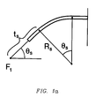
- FIG. 1a depicts one-half of one of the waveguides in the optical grating shown in FIG. 1.
- FIG. 2 shows one period Λ of the wavelength response of a fully corrected and a partially corrected apparatus like the one in FIG. 1, namely, the transmission coefficient of the path from the central input port to the central out port T0,0 as a function of Φ, the input wavelength normalized with respect to Λ and referenced to the wavelength of a transmission peak.
- FIG. 3 is a graph showing the pattern of
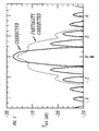
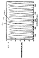
T 0,₀ for a multiplexer optimized for N = 10 and M = 11 compared with a nonoptimized pattern. Also shown are the optimized patterns T0,0 for N = 7 and M = 11 and 15. - FIG. 4 is a graph showning the patterns T0,q for an optimized multiplexer with N = 7 and M = 15.
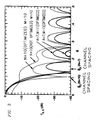
- FIG. 5 shows measured TM transmission coefficient patterns T0,0 and T0,1 of an optimized 11x11 multiplexer. The channel spacing is 1.5nm.
- FIG. 6 shows measured TM transmission coefficient patterns T0,0 and T0,1 of an optimized 7x7 multiplexer. The channel spacing is 3.3nm.
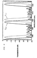
- FIG. 7 shows measured TM transmission coefficient patterns T0,q an optimized 11 x 11 multiplexer. The period A is about 16.4nm.
- FIG. 8 shows measured TM transmission coefficient patterns T0,q of an optimized 7x7 multiplexer. The period Λ is about 23.1 nm.
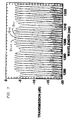
- FIG. 1 shows an example of an optical interconnection apparatus which can be used as an optical switch, multiplexer, or demultiplexer in accordance with this invention. It preferably comprises two substantially identical and symmetrically disposed
star couplers - FIG. 1 shows an
array 16 of N input waveguides radially directed from N input ports toward a focal point F2. Each of the input waveguides has a predetermined width W and is angularly displaced from its adjacent waveguides by an angle α. - The
star coupler 10 comprises adielectric slab 18 which forms a free space region having two curved, preferably circular,boundaries array 16 are connected to thefree space region 18 in a substantially uniform fashion alongboundary 18a. As indicated in FIG. 1, each of those waveguides is separated from its neighbors by a distance t along theboundary 18a. - An
array 20 of M output waveguides is radially directed toward a focal point F1. Each of the waveguides in thearray 20 has a width W′ and is separated from adjacent waveguides in thearray 20 by an angular spacing α′. The output waveguides in thearray 20 are connected to thefree space region 18 in a substantially uniform fashion alongboundary 18b. Each of the output waveguides is separated from its neighbors at theboundary 18b by a distance t′, as shown in FIG. 1. - The M waveguides of the grating 14 are a symmetric arrangement of waveguides each having lengths ℓs, where s is referenced to the central waveguide in the grating. As shown in FIG. 1a, each half of the grating 14 comprises preferably three sections, respectively composed of radial, circular, and equispaced parallel waveguides. The total length of the s-th waveguide is ℓs = 2Rs(ϑs - sinϑs) + 2ts (1 - cosϑs)+ho where ho is a constant and Rs is the s-th radius of curvature.
- Each of the output waveguides in the
array 20 is connected to the input of a waveguide in the grating 14. The length of each waveguide in the grating differs from the lengths of all the other waveguides in the grating so that in effect preditermined and different phase shifts are applied to optical signals propagating into the waveguides of the grating from thestar coupler 10 because of the different path lengths over which the signals in the grating must travel in reaching the output of the grating. The outputs of the waveguides in the grating 14 thus have different phases, which are functions of the lengths of the waveguides. - The outputs of the waveguides in the grating 14 are connected to another
array 22 of M input waveguides which are radially directed toward a focal point F4. Thearray 22 connects the output of the grating 14 to the input of thesecond star coupler 12. Likestar coupler 10,star coupler 12 comprises a slab ofdielectric material 24 forming a free space region having two curved, preferably circular,boundaries array 22 of input waveguides is connected to the free space region in a substantially uniform distribution alongboundary 24a. - An
array 26 of N output waveguides are radially directed from N output ports toward a focal point F3. The output waveguides in thearray 26 are connected to thefree space region 24 in a substantially uniform distribution along theboundary 24b. - Phase errors caused by mutual coupling between neighboring waveguides in the
arrays array 16, F2 is located at the phase center S1 ofarray 20, F3 is located at the phase center S4 ofarray 22, and F4 is located at the phase center S3 ofarray 26. - A phase center for an array of waveguides such as those arrays shown in FIG. 1 may be considered to be the center of a circle which most closely approximates a locus of points of equal phase for optical wavefronts emitted by the array when the array is excited from a particular input waveguide. In arrays such as those of FIG. 1 having a significant degree of mutual coupling between waveguides, the phase center generally is located outside the free space region a distance d away from the boundary of the free space region. The location of the phase center of an array of radially directed waveguides may be determined using the well known propagating beam method of computing the amplitudes and phases of radiation flowing from waveguides for any given excitation as a function of distance from the waveguides. Preferably, it is assumed that a central waveguide of one of the arrays is excited in the apparatus in FIG. 1. Assuming input excitation is applied to the central waveguide, namely, the waveguide directed through the focal point of the other array of waveguides connected to the same star coupler, the distance d is selected so as to minimize the variation in computed phase along some reference circle centered on that focal point. Various strategies may be adopted regarding this minimization. For example, d may be selected so as to reduce to zero as closely as possible the phase difference of the central waveguide and its two adjacent waveguides. Alternatively, one can select d so that the phase difference between the central and marginal waveguides is minimized, This alternative can be shown to minimize in general the peak value of the phase difference in the entire array.
- Once d has been selected in this fashion, there still may be unacceptable residual phase errors across the array of waveguides. These may be reduced by appropriately selecting the length ℓs of the arms of the grating, which results in a grating having a nonconstant length difference ℓs - ℓs-1 throughout the grating.
- The apparatus of FIG. 1 can be used as a switch, a multiplexer, or a demultiplexer. If optical power at a particular wavelength λ₁ is input to a particular input waveguide or input port in the
array 16, the optical input power spreads in thefree space region 18 and is distributed to the M waveguides in the grating 14 so that portions of the input optical power travel through each of the M waveguides. Those portions of the input optical power combine infree space region 24 in such a way that as much as possible of that power is concentrated on a desired point along theboundary 24b. This point is selected to be at a desired input of an output waveguide in thearray 26 and thereby the input optical power is launched into that selected output waveguide. The location of this concentration of power, and the identity of the output waveguide to which input optical power is directed, is a function of the wavelength of input optical power. Thus, one can select which output waveguide the input power is directed by appropriately setting the wavelength of the input power. The identity of the output waveguide to which input power is directed is also a function of the identity of the input waveguide to which that input power is directed. The apparatus of FIG. 1 can thus switch input optical power from any of the N input waveguides to any of the N output waveguides in the case of a device having N input ports and N output ports. - Notice that the transmission coefficient of the apparatus of FIG 1 is essentially a periodic function of input wavelength and, in a particular period, it has a single peak of transmission close to unity, produced from a particular input port to a particular output port. If the input and output waveguides are spaced arbitrarily, the apparatus of FIG. 1 is in general characterized in each period by N² distinct wavelengths of maximum transmission, since N² is the total number of transmission coefficients corresponding to the various input and output ports. The differences between these wavelengths are determined by the spacing of the input and output waveguides. It is important, for most applications, to choose uniform spacing, so as to cause the above N² wavelengths to essentially coalesce into N wavelengths λ₁...,λN of maximum transmission in a particular period. In the following, the device will be assumed to be arranged in this preferred configuration.
- If optical input power comprising a plurality of appropriate wavelengths λ₁,λ₂, ... λN of maximum transmission is introduced simultaneously in one of the input waveguides, each of the wavelengths spreads in free space region of
star coupler 10. Portions of the optical power are transmitted through the M waveguides of the grating 14 which then are combined in the free space region ofstar coupler 12. Optical power of each wavelength is concentrated at the inputs of different output waveguides. Each of the wavelengths of optical input power directed to a single input port thus, is output by the device in different output ports. The device thus can act as a demultiplexer of the plurality wavelengths appearing on one of the input waveguides. The order in which wavelengths appear on the output waveguides is a function of which of the input waveguides carries the plurality of input wavelengths. The order thus can be different when the input wavelengths are directed to a different input waveguides. The device of FIG. 1 thus may be used as an N x N demultiplexer in the case of a device having N input ports and N output ports.. - As mentioned above, the device of FIG. 1 is symmetrical. Therefore, if optical input power at one of a plurality of different input wavelengths λ₁,λ₂ ... λN is applied to each of the input waveguides, all of the wavelengths can be directed to a single output waveguide. The identity of the output waveguides is a function of the spatial order in which the input wavelengths are applied to the input waveguides and also a function of the magnitude of the wavelengths. The apparatus of FIG. 1 thus may be used as an N x N multiplexer in the case of a device having N input ports and N output ports.
- The location of the focal points of arrays of input waveguides at the phase centers of arrays of output waveguides and vice versa, as described above, reduces crosstalk between the channels of the device and preserves efficient power transfer between selected input ports and selected output ports of the device. This is further improved by an appropriate non-constant path length difference throughout an optical diffraction grating having appropriate length waveguides. The improved switching, multiplexing, and demultiplexing capabilities of the apparatus of FIG. 1 are useful in a wide variety of optical communication systems. These improvements may be utilized in communication systems which carry any kind of optical signals, for example, voice, data, or video signals. They may also be utilized in communication systems of various configurations such as long distance communications systems or local area networks.
- The detailed examples of the invention described below reiterate and reinforce the theoretical considerations generally alluded to above in connection with the description of FIG. 1. Additional theoretical considerations are described and the details of calculated and experimental results are reported.
- The following discussion of terminology will facilitate understanding the discussion below. FIG. 1 illustrates input optical power P directed to the pth input port. Output optical power PTp,q may be emanating from the qth output port, where Tp,q is the transmission coefficient from the pth input port to the qth output port. The values of p and q are referenced to the central input port and central output port, respectively, which, therefore, are the Oth input port and the Oth output port, respectively. The pth input port is angularly displaced from the central input port by an angle pα and the qth output port is angularly displaced from the central output port by an angle qα. Optical power Ps flows in the sth waveguide in the optical grating 14. The value of s is referenced to the central waveguide in the grating, namely, the 0th waveguide in the grating. The sth waveguide has a length ℓs and is angularly displaced in the vicinity of
arrays - Described here is an example of a design in accordance with FIG. 1 of a wavelength-selective N x N integrated multiplexer which can simultaneously multiplex and demultiplex a large number of input and output channels. The wavelength response of the multiplexer is periodic, with period Λ. In each period, the multiplexer accepts, from each input port, a total of N wavelength channels that are demultiplexed and transmitted efficiently to the N output ports. Similarly, each output port receives, in each period Λ, N channels, one from each input port. Such a multiplexer can be realized, in accordance with FIG. 1, by means of two N x M star couplers combined with a lens waveguide consisting of M waveguides of different lengths acting as a diffraction grating between the two couplers. However, as described above, such an arrangement consisting of waveguide arrays is in general afflicted by aberrations, caused by mutual coupling between input and output waveguides or between waveguides connected to the grating. An undesirable consequence of mutual coupling is that some of the input signal intended for a particular output port will, in general, be also transmitted to other ports, thus causing undesirable crosstalk. Another consequence is a reduction of the multiplexer efficiency. It is, of course, possible to reduce mutual coupling by increasing the spacing of the input and output waveguides or the spacing of those waveguides connected to the grating. This, however, will reduce the total number N of channels that can be fitted in a given period Λ and it will also reduce the efficiency of the grating, as will become clear from the following discussion. Accordingly, described here are the details of a correction scheme that substantially reduces aberrations caused by mutual coupling, thus allowing nearly ideal wavelength response to be produced, using strongly coupled waveguides.
- A multiplexer like the one in FIG. 1 is particularly suitable for realization in integrated form by using SiO₂/Si technology. Specifically, the waveguides, star couplers, and optical grating comprise SiO₂ regions patterned on an Si substrate, for example, by photolithographic techniques. The multiplexer should be useful for both long haul and local area networks. In a local area network, it allows a large number of receivers and transmitters to be efficiently interconnected. Unlike broadcasting-star configurations, it has no associated 1/N division loss. It is a wavelength routing device whose transfer matrix allows the same wavelength to be used simultaneously at any number of input ports, with the corresponding signals appearing at different output ports. Thus, by employing N tunable lasers, each capable of covering N wavelengths, the multiplexer can also be used as an N x N switch. Two designs are particularly important.
- One design is characterized by the largest possible N for a given grating aperture. This design is very efficient, since most of the signal power applied to any particular input port is transferred to the output ports, and this is obtained, essentially, at all wavelengths in each period Λ (free spectral range) of the multiplexer. This multiplexer is, however, afflicted by relatively high levels of crosstalk and, therefore, it may require use of additional input and output filters. The second design, on the other hand, provides very low levels of cross-talk, but it requires a relatively large channel separation, at least twice the channel width. An important feature of this design is its excellent frequency response, whose sidelobes are substantially reduced (to very low levels, of less than -30 dB) by properly optimizing the aperture distribution of the grating. Such a multiplexer, with greatly reduced sidelobes, will be particularly useful when the number of channels N is large, since interference then becomes the most important limitation that determines the largest feasible N.
- The multiplexer of FIG. 1 must satisfy two well-known conditions. First, in order for the multiplexer to be efficient, most of the power supplied to each input waveguide must be transferred to the waveguides of the grating. Second, the input waveguides must be located within the central Brillouin zone of the grating. In FIG. 1 the grating is composed of M uncoupled waveguides, connected to radial waveguides having angular spacing α′. Therefore, the angular width 2γ′ of the central zone specifying the field of view of the grating is determined by the relation 2γ′ α′ ≃λ/R where R is the distance from F₁ to F₂. In order for the grating to perform effciently in the above field of view, the radial waveguides of the grating must be strongly coupled in the vicinity of the free-space region.
- Furthermore, the grating angular aperture must be large enough to intercept the entire incident power radiated by the input array. That is, Mα′ must exceed the angular width 2γ of the field radiated in the free-space region by each input waveguide. The largest value of N for a given M under the above conditions is easily shown to be equal to M, and is obtained when the input and output waveguides are strongly coupled. Then, the radiation pattern of each input waveguide approaches in the free-space region a rectangular pattern, with angular width approximately equal to the width of the central Brillouin zone of the input array. Such a multiplexer, with the largest N, will also have the greatest efficiency. As pointed out later, however, it will also have relatively high sidelobes, produced by its wavelength response. These sidelobes can be reduced substantially, as shown later, by reducing N. In the following, it will be assumed that the two star couplers in FIG. 1 are properly designed, in accordance with the above criteria, so that the power supplied to each input waveguide is efficiently transferred to the M waveguides of the array. A remaining problem, then, is to cause the various wavelength components of this power to be efficiently demultiplexed, with minimal crosstalk caused by mutual coupling.
- Each array in FIG. 1 is characterized by two characteristic points, Fi,Si, which are respectively the focal point Fi of its radial lines and the phase center, Si of radiation produced by exciting the central waveguide of the array. The correction scheme requires that two conditions be satisfied. The first condition optimizes the two star couplers. It is satisfied by designing each coupler so that the phase center of each array connected to the coupler essentially coincides with the focal point of the other array connected to the coupler. The second condition minimizes residual aberrations caused by mutual coupling and it is satisfied by properly choosing the lengths ℓi of the M waveguides forming the grating. The purpose of these waveguides is to produce a constant path length difference ℓ between signals propagating in adjacent waveguides of the grating. The appropriate values of ℓ are obtained by optimizing the terminal behavior of the multiplexer at the particular wavelength for which βℓ = 2πJ, where J is the order of the array, and β is the propagation constant of the the waveguides. At this wavelength, the multiplexer transmission coefficient must be optimized for two particular ports, those corresponding to the central waveguides containing the foci F₁ ,F₂ andF₃ ,F₄ of the two couplers. In order to maximize the output signal, the lengths ℓi must be properly chosen, so that the various signal components corresponding to the M waveguides all contribute in phase, except for multiples of 2πJ caused by the grating order. Most of the input power will then be transferred to the output port under consideration. Therefore, since negligible input power will be transferred to other ports, it will contribute negligible crosstalk. Furthermore, once the multiplexer is optimized for the central ports, it will perform efficiently, with negligible crosstalk, also from the other ports. This is a consequence the first condition of the correction scheme, which is now explained in greater detail.
- Consider two particular ports of the multiplexer, the pth input port and the qth output port. The corresponding transmission coefficient is best derived, according to the Lorentz reciprocity theorem, by exciting the multiplexer from these two ports and determining the signals then produced in the M waveguides. The two sets of signals propagate in opposite directions. Furthermore, on the multiplexer symmetry line, the signals produced by exciting the qth output port are simply the complex conjugates of those produced by exciting the qth input port. Let Ai,φi denote the amplitudes and phases produced, on the symmetry line, by the p-th port. In order to obtain a perfect match (unity coupling) between the above two sets of signals at the wavelengths of maximum transmission, Ai, φi must essentially satisfy three conditions. First, Ai must be independent of p. Second, the difference φi-φi-1 must vary linearly with p. Third, φi-φi-1 must be independent of i. The correction scheme simply insures to a good approximation these three conditions. Because of the last condition, maximum transmission is produced at the wavelengths for which φi-φi-1 is an integer multiple of 2π. The other two conditions are satisfied, to a good approximation, by properly choosing the locations of the foci F₁ and F₂. In the absence of mutual coupling, the optimum locations are well-known. They are obtained by simply placing F₁ andF₂ at the boundaries of the free-space region. Also known is what will happen if this condition is not satisfied. Then, a displacement d of F₁ from the boundary will cause phase errors

for p = 0. It will also cause the normalized amplitudes Ai/Ao to become functions of p. A similar result will be caused by a displacement of F₂ which will produce in Ai an additional dependence on p. Such a multiplexer cannot be efficient from all ports. Now consider the effect of mutual coupling in a coupler having its foci located at the boundary of the free space region. By exciting the central waveguide, one will find that the wavefronts radiated in the free space region will not be centered at F₁. That is, their center of curvature be displaced from the boundary, and the displacement will affect both Ai and φi. In order to correct these aberrations, which are a consequence of mutual coupling, the focus of each array must be displaced from the boundary, so that it coincides with the phase center of the other array. The optimum location of d is simply obtained by minimizing the above phase errors produced for p = 0. The other focus F₂, on the other hand, must be chosen so that approximately the same Ai are produced for all p. In practice, it will be sufficient to satisfy this condition for two particular values of p, those corresponding to the marginal ports. - The importance of the above conditions in the multiplexer design is illustrated in FIG. 2 showing the calculated wavelength response of an integrated SiO₂/Si multiplexer optimized by this technique, compared to the response of a multiplexer that was not fully optimized. In the first fully optimized case, in order to obtain the desired response, the foci had to be displaced from the free space region by 350 µm. In the latter case, the displacement was reduced by 200µm, to show the effect of mutual coupling. The free space region of each coupler in this example is assumed to have a length R of 1350 µm, the waveguides are strips of constant width W = W′ = 5 µm, with refractive index n₁ ≃ 1.44 separated by refractive index n₂ ≃ n₁ - 0.003 between the strips. The final gaps t = t′ between adjacent waveguides, at the circular boundaries of the free space regions, are 3µm.
- The above correction scheme is particularly important when N is large. Then, the angular separation a of the input waveguides becomes small, for a given angular width γ′ of the grating field of view. One can show that the phase errors φi-φi-1 produced for p = 0 increase linearly with the length of the interaction region characterized by appreciable coupling between adjacent input waveguides. This length increases linearly with 1/α, for given values of W and W + t. It is then difficult to avoid mutual coupling between the waveguides of the input and output arrays, even if relatively large values of W and t are used Furthermore, W cannot be chosen too large, since this could substantially increase the multiplexer dimensions, thus reducing substantially the largest N that can be realized for a given wafer size.
- The above correction scheme has been described for the particular grating of FIG. 1. Clearly, however, the same scheme can be applied to a different grating. Then, crosstalk caused by mutual coupling between the input and output waveguides can be essentially removed by properly choosing the locations of the foci of the input and output waveguides, and by properly designing the grating so that it corrects (for instance by means of a suitable lens or reflector) the phase errors caused, by mutual coupling, over the grating aperture Mα′.
- Once the multiplexer of FIG. 1 is optimized using the above correction scheme, it will demultiplex, in each period Λ of its wavelength response, a total of N input channels. The spacing of the channels corresponding to a particular input port is determined by the output waveguide spacing. Similarly, the spacing of the N channels transferred to a particular output port is determined by the spacing of the input waveguides. Nonuniform spacing may be desirable for some applications, and this may be accomplished by properly designing the input and output arrays. The largest N that can be realized for a given M is obtained when the input and output waveguides are closely spaced. This will also minimize the multiplexer insertion loss, since it will maximize the efficiency of power transfer by each coupler. However, such a multiplexer will have an undesirable feature, its wavelength response will be afflicted by relatively high sidelobes, causing crosstalk at wavelengths different from those of maximum transmission. This is a consequence of the rectangular pattern of illumination approximately produced by the input waveguides, as explained above. The sidelobes can be substantially reduced, however, by using the following procedure. For this purpose, one must increase the width W and gap t of the input waveguides, thus reducing the value of N for a given M. The optimum width producing approximately the lowest sidelobes is approximately attained when the first two zeroes, or approximate zeroes, of the input array radiation pattern are approximately produced in the directions corresponding to the marginal waveguides of the grating. More precisely, one must produce approximately a cosine distribution, so that

- Described here is a design of another integrated N x N multiplexer capable of simultaneously multiplexing and demultiplexing a large number (up to about 50) of input and output wavelength channels. The multiplexer is a generalization of the 2 x 2 Mach-Zehnder multiplexer. It consists of two N x M star couplers connected by M paths of unequal length. Aberrations caused by mutual coupling in the waveguide arrays are minimized by a correction scheme that causes each star coupler to accurately perform a Fourier transformation. The multiplexer is useful as a wavelength routing device for long haul and local area networks.
- The design of an N x N multiplexer is suitable for realization in integrated form for large N using the SiO₂/Si technology described above. It comprises two star couplers connected by M uncoupled waveguides having unequal lengths ℓs forming a grating, as shown in FIG. 1. Each coupler is realized by using a planar arrangement of two confocal arrays of radial waveguides performing with efficiency approaching 100% under ideal conditions, when the waveguides have strong mutual coupling. Aberrations caused by mutual coupling are minimized by a correction scheme which causes each star coupler to accurately perform a finite Fourier transformation. It is possible, by using this scheme, to obtain good efficiency in the entire Brillouin zone of the grating, as demonstrated by experimental results. Such a multiplexer should be useful as a wavelength routing device, for both long haul and local area networks. Its input-output mapping allows the same wavelength to be applied simultaneously to any number of input ports, with the corresponding signals appearing at different output ports. Thus, by employing N tunable lasers, each capable of N wavelengths, the multiplexer can be used as an N x N switch.
- The multiplexer of FIG. 1 is a symmetric arrangement of two identical couplers and a grating comprising M uncoupled waveguides with propagation constant β. The first coupler comprises two periodic arrays of radial waveguides with foci F₁ andF₂ and the second coupler comprises two periodic arrays of radial waveguides with foci F₃ and F₄. The waveguides are strips of constant refractive index n₂ separated by strips of refractive index n₁. Each focus Fi is displaced (by d or d′) from the circular boundary of the free-space region, which also is characterized by uniform refractive index n₂. The input power P supplied to the p-th port at a particular wavelength λ is transferred to the grating with efficiency εp = (ΣPs)/P where Ps is the power in the s-th arm of the grating. For an optimized multiplexer, neglecting residual aberrations, the power transmission coefficient Tp,q from the p-th input port to the q-th output port is Tp,q = |ΣPsexp(jφs)|² /P² where the phases φs are determined by the lengths ℓs of the grating arms. These lengths have been properly chosen so as to effectively produce a constant path length difference ℓ between adjacent paths. Therefore, the difference φ = φs - φs-1 is essentially independent of s, and one finds that


where
The above relation assumes that the multiplexer is entirely free of aberrations. Then, the multiplexer efficiency, given by the largest value of Tp,q, is just the product εpεq of the efficiencies of the two couplers. This can be justified as follows. According to Lorentz reciprocity theorem, the transmission coefficient Tp,q is determined by the coupling coefficient between two supermodes, produced in the grating (in opposite directions) by exciting the two ports p and q. By then assuming a perfect match (unity coupling) between the two modes, one obtains Tp,q = εpεq. This, however, requires two conditions. First, the total optical path φs between the two ports p and q must be independent of s. Second, the relative powers Ps/P₀ must be independent of p,q. These conditions can be realized to a good approximation by optimizing the locations of the foci Fi described above. - Consider, in the grating, the signals produced for p = 0 on a reference circle centered at F₁. Mutual coupling between the input waveguides will affect the phases of these signals. It will cause phase errors δφs, which must be minimized by optimizing the location of F₁. The optimum location of F₁ can be determined and it is called the phase center of the input array. Similarly, the optimum location of F₂ is the phase center of the second array. The optimum location of F₃ and F₄ with respect to the waveguide arrays connected to the other coupler are similarly determined. One can show, once the two foci of each coupler are properly optimized, that each coupler becomes approximately equivalent to a confocal arrangement of two arrays without mutual coupling between the waveguides of each array and, as a consequence, one obtains approximately Eqs. (1-3). Although aberrations will be substantially reduced, they will not be entirely eliminated, however, by simply optimizing the two foci. These residual aberrations may be reduced by properly choosing the lengths ℓs. The above conditions, optimizing respectively the two foci and the lengths ℓs, comprise the most complete correction scheme. In general, a multiplexer with its foci displaced from their optimum locations, will have aberrations, reducing efficiency and increasing crosstalk, as shown in one of the examples given later. One can show that a small longitudinal displacement of F₁ will cause δφs≃kQd(α′s)²/2. A displacement of F₂, on the other hand, will primarily affect the powers Ps. It will cause a lateral displacement δxp≃ pαδd′ of the incident field illuminating the second array, thus causing Ps to vary with p. There is a simple relation existing (approximately) between channel spacing Φ₀, the total number N of channels in a period, and the focal length R. From eqs. (1-3), the transmission coefficient T0,1 is displaced from T0,0 by Φo = kRαα′. Furthermore, h(φ) is periodic with period 2π and, therefore, the total number of channels in a period is λ/(Rαα′). This is also the total number of input waveguides in the central Brillouin zone of the grating. In fact, the angular width of this zone is λ/(Rα′) and, therefore, dividing it by the angular spacing α, we obtain the desired result. Notice that N is not in general an integer, and it varies with λ.
- Ideally, one would like the sidelobes of h to be very low and, at the same time, one would like N to be as large as possible, for a given M, so as to minimize the channel spacing, thus maximizing the total number of channels. The largest N is clearly M, and it can be realized efficiently by using efficient arrays, so that Ps/P₀≃1. Then for N≃M

giving the smallest channel spacing, which is then approximately equal to the channel width determined by the 3dB points of |h|². However, h in this case is afflicted by relatively high sidelobes. In order to substantially reduce them, one must increase the channel spacing by approximately a factor 1.7, and choose M≃2N, as illustrated below. - Initially, let all arrays be designed efficiently by using SiO₂/Si waveguides with cores of width W≃5µm and Δn≃0.003. In the vicinity of the free space regions, assume gaps tof3µm between the cores, and let the design wavelength be λ≃λ/n= 1.3µm. The number N of input waveguides in the central Brillouin zone of the grating is determined by the focal length R. In the following example we choose R≃1350µm, resulting in N≃10. By calculating the input array radiation characteristics, by a propagating beam method, one can determine the amplitudes and phases in the various arms of the grating. By then optimizing the location of F₁ one finds that the displacement of each phase center from the free-space region is accurately given by

giving d≃350µm for R = 1350µm. FIG. 3 shows the behavior of T0,0 for a multiplexer optimized by the propagating beam method for N = 10 and M = 11. Also shown is the effect of reducing d by 200 µm. The resulting aberrations caused by mutual coupling distort the main lobe, reducing efficiency and increasing crosstalk. - In the above example, the input array approximately produced the same power in each arm of the grating. We next produce approximately a cosine distribution, so that


showing that the multiplexer performs well in the entire central zone of the grating, i.e. in the entire spectral range determined by the period of h(φ). Notice that the marginal efficiencies for the input and output ports corresponding to the edges of the above zone are substantially lower, as expected because of Bragg reflections. - The multiplexer performance of typical values of W and t have been discussed. A relatively small focal length R≃1350µm has been chosen, resulting in N = 7-10. Greater N will be obtained by choosing a larger R, since N increases linearly with R, for given values of W and W + t. However, aberrations also increase linearly with R, and this must be taken into account in the design. Then, for large N, mutual coupling between the input and output waveguides is difficult to avoid, even for large N, and the technique of correcting aberrations then becomes particularly important. The next example describes the measured performance of two multiplexers based on the above designs.
- The performance of an integrated N x N multiplexer fabricated using SiO₂/Si waveguides was measured. The insertion loss for N=7 is typically lower than 2.5 dB and crosstalk is less than -25 dB. The multiplexer response is approximately periodic. In each period the multiplexer accepts, from each input waveguide, a total of N channels, and it transmits efficiently each channel to a particular output port. Similarly, each output port receives N channels, one from each input port. Thus, the total number of channels that can be transmitted simultaneously is N², which requires only N optical frequencies.
- Reported here is the measured performance of an integrated N x N multiplexer fabricated using SiO₂/Si waveguides. The multiplexer response is approximately periodic, with period A. In each period the multiplexer simultaneously multiplexes and demultiplexes a total of N² channels. Thus, each output port receives N channels, one from each input port. The same wavelength can be used simultaneously at all input ports, since the corresponding signals appear at different output ports. Thus, by employing N tunable lasers, each capable of cover N wavelengths, the multiplexer can be used as an N x N switch. Furthermore, unlike broadcasting star couplers, there is no 1/N splitting loss.
- The multiplexer comprises of two identical star couplers combined with M waveguides acting as a grating between the two couplers, as shown in FIG. 1. When operated from a particular input port, it performs as an ordinary 1xN demultiplexer. It differs, however, from previous designs, because of its good performance in the entire period Λ. This is obtained by using the correction scheme described above to minimize aberrations caused by mutual coupling between adjacent waveguides in the various arrays. Several integrated multiplexers, with N=7 and N=11 have been fabricated, and their measured performance agree well with calculations based on the propagating beam method mentioned above. For N=7, the total insertion loss, from input to output fiber, is typically lower than 2.5 dB. Crosstalk is typically less than -25 dB. It is expected that similar results will be obtained for larger N. The multiplexer should therefore, be useful as a wavelength routing device, for both long haul and local area networks, and perhaps also for packet switches.
- The multiplexer comprises two identical star couplers combined with M waveguides forming a grating between the two couplers, as shown in FIG. 1. Each coupler consists of a dielectric slab forming a free-space region between two periodic arrays of radial waveguides, which emanate from the virtual foci Fi. In the vicinity of the free-space region, the waveguides are closely spaced. As a consequence, mutual coupling between adjacent waveguides causes aberrations, which affect the coupler transmission matrix, and must be minimized by using the previously noted correction scheme. To this purpose, the foci of each coupler must be optimized by properly choosing their distance d,d′ from the free-space region. The optimum d, for instance, is obtained by exciting the central port of the first coupler, and then minimizing the calculated phase errors produced, in the grating arms, on a reference circle centered at F₁. After minimizing the phase errors caused by the two couplers, residual phase errors may be further reduced by optimizing the lengths ℓs of the grating arms. Notice, because of this, the optimized grating is not exactly characterized by a constant difference ℓs - ℓs-1 throughout the grating.
- The multiplexer operates as follows: The input signal supplied to the p-th port is radiated in the free-space region, and most of its power is accepted by the grating. Some of this power is then transferred by the second coupler to the q-th output port. The purpose of the grating is to provide a constant path length difference ℓ≃ℓs - ℓs-1 between adjacent paths connecting the two couplers. This causes a difference in phase φ = βℓ that increases with the propagation constant β≃2π/λ. Hence, it causes the power transmission coefficient Tp,q to essentially vary periodically with 1/λ, producing peaks of maximum transmission at the wavelengths for which φ is an integer multiple of 2π. Here, we show that it is possible, by using the correction scheme of this application, to obtain improved performance in the entire period A (the free spectral range determined by ℓ).
- The above scheme insures a good match between the two couplers at the wavelengths of maximum transmission. Thus, the multiplexer efficiency becomes, to a good approximation, the product of two quantities, the efficiencies εp andεq of the two couplers. One of these, εp, is the fraction of the input power that is transferred to the grating. Similarly, by reversing the sense of transmission, εq is the efficiency of power transfer from the q-th port to the M waveguides of the grating. The product εpεq is approximately the multiplexer efficiency εp,q corresponding to the maximum value of Tp,q. The wavelength dependence of Tp,q is specified by the Fourier transform of the coefficients Cs = Ps/P₀, where Ps denotes the power transferred from the p-th input port to the s-th waveguide of the grating. As a consequence, the main properties of Tp,q, such as the with of the main lobe and the level of the sidelobes, are determined by the radiation characteristics of the input array. Hence, they are determined by the width W and the spacing W + t of the input waveguides. As discussed above, the design producing efficiently the narrowest response and the smallest channel spacing is obtained by using an input array with strongly coupled waveguides, arranged with minimal gaps t. This will maximize the number of channels (for a given grating) but it will also produce relatively high sidelobes. In order to reduce these sidelobes, one must reduce N. Here, we describe the measured performance of two multiplexers designed using two different approaches, by maximizing N using closely spaced waveguides in one case and, in the other case, by minimizing the sidelobes.
- In the first case, the same values of W and t were chosen for all arrays. The cores had a constant width W = W′= 5µm with gaps t = t′ with 3µm between the cores in the vicinity of the free-space region. The cores were realized with a refractive index difference Δn≃0.0035. The first design was characterized by N = 11 and M = 11. In case of N = 11 and M = 11, the distances between focal point F1 and
boundary 18a, between focal point F2 andboundary 18b, between focal point F3 andboundary 24a, and between focal point F4 andboundary 24b were all 350 µm. - In the second design, the width and spacing of the input waveguides were increased by choosing N = 7, W≃10µm and t≃6µm, thus substantially reducing the sidelobes. Several multiplexers having this value of N with values of M of 11, 13 and 15, were made. In the cases of N = 7 and M = 11, 13, and 15, the distances between focal point F1 and
boundary 18a and between focal point F4 andboundary 24b were both 20 µm. The distances in those three situations involving N=7 between focal point F2 andboundary 18b and between focal point F3 andboundary 24a were both 350 µm. The three multiplexers gave similar performance, but lower sidelobes were obtained for M = 15. To simplify the discussion here, the performance obtained in two cases are shown, for N = 11, M = 11, Λ≃16.5nm and N = 7,M = 15, Λ≃23.1 nm. - In both cases, the patterns ofTp,q varied little with p,q, and the insertion losses were approximately given by


For p≠0, the insertion losses εp,q are approximately given by
- The transmission coefficients Tp,q for a multiplexer without aberrations are determined by the Fourier transform of the coefficients Ps/Pt, where Pt denotes the total input power and Ps is the power transferred to the s-th waveguide of the grating. The values of Ps were measured by cleaving a multiplexer along the symmetry line, and these values were used to determine the multiplexer performance obtainable by removing all phase errors caused in the grating by residual aberrations. The results agreed well with the calculated patterns. In particular, for N = 7, the sidelobes were lower than -32 dB. The higher sidelobes in FIG. 7 were primarily caused by phase errors, of less than 0.05λ, which may be corrected by slightly modifying the lengths ℓs.
- The results described above demonstrate that it is possible, by using two star couplers, to realize an N x N multiplexer analogous to the 2x2 Mach-Zehnder interferometer. By using strongly coupled input and output waveguides, the channel spacing can be made to approach the channel width, and the response Tp,q is then given approximately by |sin(Nφ/2)/[Nsin(φ/2]|². The results obtained for N = 7 show, furthermore, that the sidelobes of Tp,q can be substantially reduced by choosing M≃2N and increasing the channel spacing by about a factor 1.7. An important feature of both designs, is that they make full use of the entire available field of view of the grating.
Claims (10)
- An optical interconnection apparatus comprising:
a first plurality of input waveguides radially directed from a plurality of input ports toward a first focal point;
a first star coupler having an input connected to the plurality of input waveguides;
a first plurality of output waveguides radially directed to a second focal point and connected to an output of the first star coupler,
an optical grating comprising a plurality of unequal length waveguides having inputs connected to the first plurality of output waveguides;
a second plurality of input waveguides radially directed to a third focal point and connected to outputs of the optical grating;
a second star coupler having an input connected to an output of the second plurality of input waveguides; and
a second plurality of output waveguides radially directed from a plurality of output ports toward a fourth focal point and connected to an output of the second star coupler,
the first and second focal points being located predetermined distances from the first star coupler and the third and fourth focal points being located predetermined distances from the second star coupler. - The optical interconnection apparatus of claim 1, in which the predetermined distances of the focal points from the star couplers are such that phase errors are reduced.
- The optical interconnection apparatus of claim 1, in which the predetermined distances of the focal points from the star couplers are such that aberrations caused by mutual coupling between waveguides is reduced.
- The optical interconnection apparatus of claim 1, in which the input and output radially directed pluralities of waveguides each define respective phase centers;
the focal points of the input waveguides substantially coincide with the phase centers of the output waveguides; and
the focal points of the output waveguides substantially coincide with the phase centers of the input waveguides. - The interconnection apparatus of claim 2, in which the difference in length between adjacent waveguides in the optical grating is not the same for all adjacent waveguides throughout the grating so as to reduce residual phase errors in the apparatus.
- An optical interconnection apparatus, comprising:
a free space region of predetermined geometry and;
at least one array of waveguides radially directed toward a first focal point located a predetermined distance outside the free space region so as to reduce phase errors caused by mutual coupling between the waveguides. - The optical intercomection apparatus of claim 6, further comprising:
a second array of waveguides radially directed toward a second focal point located a predetermined distance outside the free space region so as to reduce phase errors caused by mutual coupling between the waveguides in the second array. - The optical interconnection apparatus of claim 7, in which the array of waveguides directed toward a first focal point defines a first phase center and the second array of output waveguides defines a second phase center, and
the first focal point substantially coincides with the second phase center and the second focal point substantially coincides with the first phase center. - The optical interconnection apparatus of claim 7, further comprising:
an optical grating connected to the second array of waveguides and having a plurality of optical waveguides each having a predetermined length which differs from the predetermined lengths of the other waveguides in the grating, the length difference between two adjacent waveguides in the grating not being constant throughout the grating and the lengths of the waveguides in the grating being such that residual phase errors are reduced. - An optical transmission system, comprising:
a plurality of input ports at least one of which receives optical communication signals;
a plurality of output ports at least one of which transmits optical communication signals; and
an optical interconnection means between the plurality of input ports and the plurality of output ports, comprising:
a free space region of predetermined geometry and;
an array of input waveguides radially directed toward a first focal point located a predetermined distance outside and away from the free space region so as to reduce phase errors caused by mutual coupling between the input waveguides.
Applications Claiming Priority (2)
| Application Number | Priority Date | Filing Date | Title |
|---|---|---|---|
| US748131 | 1991-08-21 | ||
| US07/748,131 US5136671A (en) | 1991-08-21 | 1991-08-21 | Optical switch, multiplexer, and demultiplexer |
Publications (2)
| Publication Number | Publication Date |
|---|---|
| EP0528652A1 true EP0528652A1 (en) | 1993-02-24 |
| EP0528652B1 EP0528652B1 (en) | 1997-12-17 |
Family
ID=25008160
Family Applications (1)
| Application Number | Title | Priority Date | Filing Date |
|---|---|---|---|
| EP92307434A Expired - Lifetime EP0528652B1 (en) | 1991-08-21 | 1992-08-13 | Improved optical multiplexer, and demultiplexer |
Country Status (4)
| Country | Link |
|---|---|
| US (1) | US5136671A (en) |
| EP (1) | EP0528652B1 (en) |
| JP (1) | JP2665114B2 (en) |
| DE (1) | DE69223561T2 (en) |
Cited By (7)
| Publication number | Priority date | Publication date | Assignee | Title |
|---|---|---|---|---|
| EP0717295A3 (en) * | 1994-12-12 | 1997-07-09 | Corning Inc | MxO multiplex demultiplex component |
| WO1998057202A2 (en) * | 1997-05-17 | 1998-12-17 | HEINRICH-HERTZ-INSTITUT FüR NACHRICHTENTECHNIK BERLIN GMBH | Device for superposing optical signals with different wavelengths |
| EP0911659A1 (en) * | 1997-10-27 | 1999-04-28 | Lucent Technologies Inc. | Optical add/drop multiplexer having complementary stages |
| US6222963B1 (en) | 1997-10-27 | 2001-04-24 | Commissariat A L'energie Atomique | Phased array device or phasar and process for manufacturing this device |
| EP1150143A2 (en) * | 2000-04-24 | 2001-10-31 | Agere Systems Optoelectronics Guardian Corporation | Large NxN waveguide grating router |
| WO2002073270A1 (en) * | 2001-03-12 | 2002-09-19 | Avanex Uk Limited | Arrayed waveguide grating |
| US6724995B1 (en) | 1996-12-23 | 2004-04-20 | Tellabs Denmark A/S | Bidirectional router and a method of bidirectional amplification |
Families Citing this family (300)
| Publication number | Priority date | Publication date | Assignee | Title |
|---|---|---|---|---|
| GB9027658D0 (en) * | 1990-12-20 | 1991-02-13 | Secr Defence | Intensity dividing device |
| US5206920A (en) * | 1991-02-01 | 1993-04-27 | Siemens Aktiengesellschaft | Integrated optical arrangement for demultiplexing a plurality of different wavelength channels and the method of manufacture |
| US5212758A (en) * | 1992-04-10 | 1993-05-18 | At&T Bell Laboratories | Planar lens and low order array multiplexer |
| US5243672A (en) * | 1992-08-04 | 1993-09-07 | At&T Bell Laboratories | Planar waveguide having optimized bend |
| CA2107181C (en) * | 1992-09-29 | 1998-12-29 | Yoshiaki Tachikawa | Arrayed-wave guide grating multi/demultiplexer with loop-back optical paths |
| US5280551A (en) * | 1992-12-23 | 1994-01-18 | At&T Bell Laboratories | Backplane optical spine |
| US5373517A (en) * | 1993-02-19 | 1994-12-13 | At&T Corp. | Rapidly tunable integrated laser |
| EP0612164A1 (en) * | 1993-02-19 | 1994-08-24 | AT&T Corp. | Rapidly tunable windeband integrated optical filter |
| US5373516A (en) * | 1993-02-19 | 1994-12-13 | At&T Corp. | Rapidly tunable wideband integrated laser |
| US5339157A (en) * | 1993-02-19 | 1994-08-16 | At&T Bell Laboratories | Rapidly tunable integrated optical filter |
| US5440416A (en) * | 1993-02-24 | 1995-08-08 | At&T Corp. | Optical network comprising a compact wavelength-dividing component |
| US5329392A (en) * | 1993-03-19 | 1994-07-12 | At&T Bell Laboratories | Optical communication system with multiple fiber monitoring |
| US5341444A (en) * | 1993-03-19 | 1994-08-23 | At&T Bell Laboratories | Polarization compensated integrated optical filters and multiplexers |
| US5367586A (en) * | 1993-03-26 | 1994-11-22 | At&T Bell Laboratories | Optical delay line |
| DE4312568A1 (en) * | 1993-04-17 | 1994-10-20 | Sel Alcatel Ag | Optical hybrid switch |
| US5351325A (en) * | 1993-04-29 | 1994-09-27 | Corning Incorporated | Narrow band Mach-Zehnder filter |
| US6205268B1 (en) | 1993-05-28 | 2001-03-20 | Lucent Technologies Inc. | Arrangement of optical fiber segments for minimizing effect of nonlinearities |
| US5475780A (en) * | 1993-06-17 | 1995-12-12 | At&T Corp. | Optical waveguiding component comprising a band-pass filter |
| US5390200A (en) * | 1993-10-13 | 1995-02-14 | At&T Corp. | High power, single-frequency tunable laser |
| US5461685A (en) * | 1993-10-18 | 1995-10-24 | At&T Ipm Corp. | Optical passband filter |
| US5483369A (en) * | 1993-11-03 | 1996-01-09 | At&T Corp. | Communication systems using passive RF routing |
| US5396507A (en) * | 1993-11-15 | 1995-03-07 | At&T Corp. | Reflective digitally tunable laser |
| US5493625A (en) * | 1993-11-16 | 1996-02-20 | At&T Corp. | Fast tunable channel dropping filter |
| US5434937A (en) * | 1993-11-16 | 1995-07-18 | At&T Corp. | Optical filter having integrated transceivers |
| US5425116A (en) * | 1993-11-16 | 1995-06-13 | At&T Corp. | Tunable optical waveguide grating arrangement |
| DE59502068D1 (en) * | 1994-01-11 | 1998-06-10 | Siemens Ag | Optical arrangement of strip-shaped optical waveguides |
| US5526153A (en) * | 1994-01-21 | 1996-06-11 | At&T Corp. | Optical channel adding/dropping filter |
| US5764821A (en) * | 1994-02-06 | 1998-06-09 | Lucent Technologies Inc. | Large capacity local access network |
| US5509023A (en) * | 1994-03-10 | 1996-04-16 | At&T Corp. | Laser control arrangement for tuning a laser |
| US5412744A (en) * | 1994-05-02 | 1995-05-02 | At&T Corp. | Frequency routing device having a wide and substantially flat passband |
| US5524014A (en) * | 1994-05-23 | 1996-06-04 | At&T Corp. | Optical frequency translator |
| EP0767921B1 (en) * | 1994-06-28 | 1998-10-21 | Siemens Aktiengesellschaft | Device for spatially separating and/or bringing together optical wavelength channels |
| US5488680A (en) * | 1994-08-24 | 1996-01-30 | At&T Corp. | Frequency routing device having a wide and substantially flat passband |
| US5488500A (en) * | 1994-08-31 | 1996-01-30 | At&T Corp. | Tunable add drop optical filtering method and apparatus |
| CA2151852A1 (en) | 1994-08-31 | 1996-03-01 | Albert Kai-Sun Wong | Dynamic atm network access control using an availability parameter at each port in a network path |
| US5467418A (en) * | 1994-09-02 | 1995-11-14 | At&T Ipm Corp. | Frequency routing device having a spatially filtered optical grating for providing an increased passband width |
| US5444725A (en) * | 1994-09-30 | 1995-08-22 | At&T Ipm Corp. | Multifrequency laser |
| US5600742A (en) * | 1994-09-30 | 1997-02-04 | Lucent Technologies Inc. | Wavelength grating router with output coupler |
| CA2158599C (en) | 1994-11-04 | 2000-05-02 | Corrado Dragone | Rapidly tunable integrated laser |
| US5566014A (en) * | 1994-12-28 | 1996-10-15 | At&T Corp. | Tunable add/drop optical filter providing arbitrary channel arrangements |
| US5699176A (en) * | 1995-11-06 | 1997-12-16 | Lucent Technologies Inc. | Upgradable fiber-coax network |
| US5852505A (en) * | 1994-12-28 | 1998-12-22 | Lucent Technologies Inc. | Dense waveguide division multiplexers implemented using a first stage fourier filter |
| NL9500004A (en) * | 1995-01-02 | 1996-08-01 | Nederland Ptt | Integrated optical wavelength demultiplexer. |
| DE19506814C2 (en) * | 1995-02-27 | 2001-03-01 | Hertz Inst Heinrich | Spectral apparatus |
| US5625723A (en) * | 1995-02-28 | 1997-04-29 | Lucent Technologies Inc. | Method for reducing birefringence in optical gratings |
| US5519796A (en) * | 1995-03-06 | 1996-05-21 | International Business Machines Corporation | Gain equalization using monolithic planar waveguide grating multiplexer and demultiplexer |
| US5675675A (en) * | 1995-12-29 | 1997-10-07 | Corning Incorporated | Bandwidth-adjusted wavelength demultiplexer |
| JPH0943440A (en) * | 1995-07-28 | 1997-02-14 | Toshiba Corp | Integrated optical multiplexer/demultiplexer |
| US5629991A (en) * | 1995-08-11 | 1997-05-13 | Lucent Technologies Inc. | Method for reducing birefringence in optical gratings |
| US5689122A (en) * | 1995-08-14 | 1997-11-18 | Lucent Technologies Inc. | InP/InGaAs monolithic integrated demultiplexer, photodetector, and heterojunction bipolar transistor |
| US5623571A (en) * | 1995-08-29 | 1997-04-22 | Lucent Technologies Inc. | Polarization compensated waveguide grating router |
| US5576881A (en) * | 1995-08-29 | 1996-11-19 | Lucent Technologies Inc. | Multi-frequency optical signal source having reduced distortion and crosstalk |
| US5680490A (en) * | 1995-09-08 | 1997-10-21 | Lucent Technologies Inc. | Comb splitting system and method for a multichannel optical fiber communication network |
| US5629992A (en) * | 1995-09-14 | 1997-05-13 | Bell Communications Research, Inc. | Passband flattening of integrated optical filters |
| US5719976A (en) * | 1995-10-24 | 1998-02-17 | Lucent Technologies, Inc. | Optimized waveguide structure |
| US5579421A (en) * | 1995-11-21 | 1996-11-26 | Lucent Technologies Inc. | Optical integrated circuits and methods |
| US5604828A (en) * | 1995-11-21 | 1997-02-18 | Lucent Technologies Inc. | Multi-purpose optical integrated circuit |
| FR2743234B1 (en) * | 1995-12-28 | 1998-01-23 | Alcatel Optronics | WAVELENGTH DEMULTIPLEXER |
| US5913000A (en) * | 1995-12-29 | 1999-06-15 | Doerr; Christopher Richard | Method and apparatus for guiding optical signals |
| US5745631A (en) * | 1996-01-26 | 1998-04-28 | Irvine Sensors Corporation | Self-aligning optical beam system |
| US5706377A (en) * | 1996-07-17 | 1998-01-06 | Lucent Technologies Inc. | Wavelength routing device having wide and flat passbands |
| US5867291A (en) | 1996-10-29 | 1999-02-02 | Chorum Technologies Inc. | Programmable wavelength router |
| US6005697A (en) | 1996-07-23 | 1999-12-21 | Macro-Vision Communications, L.L.C. | Multi-wavelength cross-connect optical network |
| JP2870499B2 (en) * | 1996-08-02 | 1999-03-17 | 日立電線株式会社 | Optical wavelength multiplexer / demultiplexer |
| US5926298A (en) * | 1996-08-30 | 1999-07-20 | Lucent Technologies Inc. | Optical multiplexer/demultiplexer having a broadcast port |
| US5708753A (en) * | 1996-09-24 | 1998-01-13 | Lucent Technologies Inc. | Method of recovering from a fiber-cable cut using random splicing reconnection |
| US5742414A (en) * | 1996-09-24 | 1998-04-21 | At&T Corp. | Multiplicity of services via a wavelength division router |
| US6243200B1 (en) | 2000-03-02 | 2001-06-05 | Chorum Technologies, Inc. | Optical wavelength router based on polarization interferometer |
| US6498680B1 (en) | 1996-10-29 | 2002-12-24 | Chorum Technologies Lp | Compact tunable optical wavelength interleaver |
| US6208444B1 (en) | 1996-10-29 | 2001-03-27 | Chorum Technologies Inc. | Apparatus for wavelength demultiplexing using a multi-cavity etalon |
| US6847786B2 (en) | 1996-10-29 | 2005-01-25 | Ec-Optics Technology, Inc. | Compact wavelength filter using optical birefringence and reflective elements |
| US6545783B1 (en) | 1996-10-29 | 2003-04-08 | Chorum Technologies Lp | Optical wavelength add/drop multiplexer |
| US6163393A (en) * | 1996-10-29 | 2000-12-19 | Chorum Technologies Inc. | Method and apparatus for wavelength multipexing/demultiplexing |
| US5745616A (en) * | 1996-11-27 | 1998-04-28 | Lucent Technologies Inc. | Waveguide grating router and method of making same having relatively small dimensions |
| US5881199A (en) * | 1996-12-02 | 1999-03-09 | Lucent Technologies Inc. | Optical branching device integrated with tunable attenuators for system gain/loss equalization |
| US6016375A (en) * | 1997-01-08 | 2000-01-18 | Hill; Kenneth O. | Wavelength selective fiber to fiber optical tap |
| US5745618A (en) * | 1997-02-04 | 1998-04-28 | Lucent Technologies, Inc. | Optical device having low insertion loss |
| US5909522A (en) * | 1997-02-07 | 1999-06-01 | Lucent Technologies Inc. | Chirped waveguide grating router with focal length adjustment |
| JP2858656B2 (en) * | 1997-02-14 | 1999-02-17 | 日立電線株式会社 | Optical wavelength multiplexer / demultiplexer |
| US5845022A (en) * | 1997-02-14 | 1998-12-01 | Doerr; Christopher Richard | Double-chirped waveguide grating router with angled ports |
| US6519022B1 (en) | 1997-04-02 | 2003-02-11 | Chorum Technologies Lp | Optical routing switch using symmetric liquid crystal cells |
| EP0875776A3 (en) * | 1997-04-29 | 2000-08-16 | Lucent Technologies Inc. | Optical multiplexer having flat passbands |
| US6049644A (en) * | 1997-05-13 | 2000-04-11 | Lucent Technologies Inc. | Optical routing device having a substantially flat passband |
| US6304350B1 (en) * | 1997-05-27 | 2001-10-16 | Lucent Technologies Inc | Temperature compensated multi-channel, wavelength-division-multiplexed passive optical network |
| US5889906A (en) * | 1997-05-28 | 1999-03-30 | Lucent Technologies Inc. | Signal router with coupling of multiple waveguide modes for provicing a shaped multi-channel radiation pattern |
| US6064488A (en) * | 1997-06-06 | 2000-05-16 | Monitor Labs, Inc. | Method and apparatus for in situ gas concentration measurement |
| US6631018B1 (en) | 1997-08-27 | 2003-10-07 | Nortel Networks Limited | WDM optical network with passive pass-through at each node |
| US6301031B2 (en) | 1997-09-02 | 2001-10-09 | Agere Systems Optoelectronics Guardian Corp. | Method and apparatus for wavelength-channel tracking and alignment within an optical communications system |
| US6137939A (en) * | 1997-10-01 | 2000-10-24 | Lucent Technologies Inc. | Method and apparatus for reducing temperature-related spectrum shifts in optical devices |
| US5978539A (en) * | 1997-10-03 | 1999-11-02 | Lucent Technologies Inc. | Optical device having a temperature independent spectral response using nonplanar geometric distortion of a substrate |
| DE19744354C2 (en) * | 1997-10-08 | 2001-02-01 | Hertz Inst Heinrich | Devices for separating and superimposing light signals having different frequency components |
| US5994679A (en) * | 1997-12-19 | 1999-11-30 | Lucent Technologies Inc. | Thermal housing for optical circuits |
| US6023544A (en) * | 1997-12-24 | 2000-02-08 | Lucent Technologies Inc. | Monitoring with an optical wavelength router |
| US6014390A (en) * | 1998-01-30 | 2000-01-11 | Lucent Technologies Inc. | Tunable transmitter with Mach-Zehnder modulator |
| GB2334594A (en) * | 1998-02-20 | 1999-08-25 | Fujitsu Telecommunications Eur | Arrayed waveguide grating device |
| AUPP208398A0 (en) * | 1998-03-02 | 1998-03-26 | University Of Melbourne, The | An optical device for dispersion compensation |
| US6031948A (en) * | 1998-03-03 | 2000-02-29 | Applied Fiber Optics, Inc. | Fused-fiber multi-window wavelength division multiplexer using an unbalanced Mach-Zehnder interferometer and method of making same |
| US6052499A (en) * | 1998-03-09 | 2000-04-18 | Lucent Technologies Inc. | Optical demultiplexer filter system to eliminate cross-talk side-lobes |
| US6351581B1 (en) * | 1998-03-17 | 2002-02-26 | Agere Systems Optoelectronics Guardian Corp. | Optical add-drop multiplexer having an interferometer structure |
| US6141467A (en) * | 1998-03-18 | 2000-10-31 | Lucent Technologies Inc. | Wavelength-division-multiplexing programmable add/drop using interleave-chirped waveguide grating router |
| US5937113A (en) * | 1998-04-17 | 1999-08-10 | National Research Council Of Canada | Optical grating-based device having a slab waveguide polarization compensating region |
| KR100274804B1 (en) * | 1998-04-22 | 2001-01-15 | 윤종용 | Bi-directional optical wavelength multiplexer and demultiplexer |
| US6058233A (en) * | 1998-06-30 | 2000-05-02 | Lucent Technologies Inc. | Waveguide array with improved efficiency for wavelength routers and star couplers in integrated optics |
| CA2307340A1 (en) * | 1998-08-24 | 2000-03-02 | The Furukawa Electric Co., Ltd. | Arrayed waveguide grating type optical multiplexer/demultiplexer |
| JP3895480B2 (en) * | 1998-09-25 | 2007-03-22 | 古河電気工業株式会社 | Optical wavelength multiplexer / demultiplexer |
| US5987050A (en) * | 1998-11-16 | 1999-11-16 | Lucent Technologies, Inc. | Laser transmitter based on a coupler and having a controlled output port |
| US6240118B1 (en) * | 1998-11-16 | 2001-05-29 | Lucent Technologies Inc. | Multichannel laser transmitter with a single output port |
| US6195482B1 (en) | 1998-12-29 | 2001-02-27 | Lucent Technologies Inc. | Waveguide grating router |
| KR100322125B1 (en) | 1999-01-14 | 2002-02-04 | 윤종용 | AWG module and method for monitoring optical signal using AWG module |
| US6602000B1 (en) * | 1999-02-19 | 2003-08-05 | Lucent Technologies Inc. | Reconfigurable add/drop for optical fiber communication systems |
| US6205273B1 (en) | 1999-03-02 | 2001-03-20 | Lucent Technologies Inc. | Waveguide grating router having a predetermined composite amplitude spectrum |
| CA2372401C (en) * | 1999-05-21 | 2005-05-17 | British Telecommunications Public Limited Company | Arrayed waveguide gratings |
| US6192169B1 (en) | 1999-05-28 | 2001-02-20 | Lucent Technologies Inc. | Enclosure for optical integrated circuit |
| US7127172B1 (en) | 1999-06-02 | 2006-10-24 | Massachusetts Institute Of Technology | Optical frequency filter |
| US6243507B1 (en) | 1999-06-07 | 2001-06-05 | At&T Corp. | Connection-verification in optical MEMS crossconnects via mirror-dither |
| US6292600B1 (en) | 1999-06-07 | 2001-09-18 | At&T Corp. | Angular-precision enhancement in free-space micromachined optical switches |
| US6321001B1 (en) | 1999-06-18 | 2001-11-20 | Trw Inc. | Wavelength division multiplexed optical communication system |
| JP4250811B2 (en) * | 1999-06-25 | 2009-04-08 | 日立電線株式会社 | Optical wavelength multiplexer / demultiplexer |
| US6442311B1 (en) | 1999-07-09 | 2002-08-27 | Agere Systems Guardian Corp. | Optical device having modified transmission characteristics by localized thermal treatment |
| EP1076252A1 (en) | 1999-08-13 | 2001-02-14 | Alcatel | Adjusted integrated optical multiple beam interferometer |
| ATE386281T1 (en) * | 1999-09-28 | 2008-03-15 | Corning Inc | ATHERMAL WAVEGUIDE GRID MULTIPLEXER (AWG) WITH POLYMER SEGMENT AND CORRESPONDING PRODUCTION PROCESS |
| US6236781B1 (en) | 1999-09-30 | 2001-05-22 | Agere Systems Optoelectronics Guardian Corp. | Duplicated-port waveguide grating router having substantially flat passbands |
| US6519059B1 (en) * | 1999-09-30 | 2003-02-11 | Lucent Technologies Inc. | Wavelength division add/drop multiplexer |
| US6594049B1 (en) * | 1999-10-29 | 2003-07-15 | Lucent Technologies Inc. | Optical router |
| US6385373B1 (en) | 1999-10-29 | 2002-05-07 | Lucent Technologies Inc. | Compensated cascaded waveguides |
| US6343866B1 (en) * | 2000-05-23 | 2002-02-05 | Fujitsu Limited | Optical apparatus which uses a virtually imaged phased array to produce chromatic dispersion |
| US6421481B1 (en) | 2000-02-04 | 2002-07-16 | Zolo Technologies, Inc. | Apparatus and method for producing a flat-topped filter response for diffraction grating (De) multiplexer |
| JP3566940B2 (en) * | 2000-04-18 | 2004-09-15 | 古河電気工業株式会社 | Arrayed waveguide grating type optical multiplexer / demultiplexer |
| US6529649B1 (en) * | 2000-05-01 | 2003-03-04 | Lucent Technologies Inc. | Optical filter with improved crosstalk rejection |
| US6434303B1 (en) | 2000-07-14 | 2002-08-13 | Applied Wdm Inc. | Optical waveguide slab structures |
| US6553165B1 (en) | 2000-07-14 | 2003-04-22 | Applied Wdm, Inc. | Optical waveguide gratings |
| US6493487B1 (en) | 2000-07-14 | 2002-12-10 | Applied Wdm, Inc. | Optical waveguide transmission devices |
| US7171117B1 (en) * | 2000-08-25 | 2007-01-30 | Lucent Technologies Inc. | Optical router |
| US6766084B1 (en) | 2000-08-25 | 2004-07-20 | Stratos International, Inc. | Coarse wave division multiplexer |
| US6512865B1 (en) * | 2000-08-31 | 2003-01-28 | Lucent Technologies Inc. | Cross-traffic suppression in wavelength division multiplexed systems |
| US6665476B2 (en) | 2000-09-29 | 2003-12-16 | Sarnoff Corporation | Wavelength selective optical add/drop multiplexer and method of manufacture |
| US6463197B1 (en) | 2000-11-01 | 2002-10-08 | Lucent Technologies Inc. | Coupling of optical signals to misaligned waveguides on different wafers |
| US6690855B2 (en) * | 2000-12-15 | 2004-02-10 | Nortel Networks Limited | Planar waveguide dispersion compensator |
| CA2328696C (en) | 2000-12-18 | 2008-08-12 | Jds Uniphase Inc. | Periodic arrayed waveguide grating multiplexer/demultiplexer |
| US6823096B2 (en) * | 2001-01-05 | 2004-11-23 | Lucent Technologies Inc. | Broadband optical switching arrangements with very low crosstalk |
| US6731833B2 (en) | 2001-01-16 | 2004-05-04 | T-Rex Enterprises Corp. | Optical cross connect switch |
| US6697552B2 (en) * | 2001-02-23 | 2004-02-24 | Lightwave Microsystems Corporation | Dendritic taper for an integrated optical wavelength router |
| US6563988B2 (en) | 2001-04-25 | 2003-05-13 | Lightwave Microsystems Corporation | Optical apparatus and method having predetermined group velocity dispersion |
| US6853773B2 (en) * | 2001-04-30 | 2005-02-08 | Kotusa, Inc. | Tunable filter |
| US20030020926A1 (en) * | 2001-05-15 | 2003-01-30 | Nicolae Miron | Tunable band pass optical filter unit with a tunable band pass interferometer |
| CN1191481C (en) * | 2001-05-25 | 2005-03-02 | 李志扬 | Waveguide array interferometer |
| US6778739B1 (en) | 2001-07-05 | 2004-08-17 | Calient Networks | Wavelength selective optical switch with aligned input and output substrates |
| EP1421421A4 (en) * | 2001-07-20 | 2005-10-05 | Essex Corp | Method and apparatus for optical signal processing using an optical tapped delay line |
| US6778728B2 (en) * | 2001-08-10 | 2004-08-17 | Corning Intellisense Corporation | Micro-electro-mechanical mirror devices having a high linear mirror fill factor |
| US6766074B1 (en) | 2001-08-15 | 2004-07-20 | Corning Incorporated | Demultiplexer/multiplexer with a controlled variable path length device |
| US6678446B1 (en) * | 2001-10-03 | 2004-01-13 | Lightwave Microsystems Corporation | Multi-band arrayed waveguide grating |
| US6879749B2 (en) * | 2001-11-27 | 2005-04-12 | Ec-Optics Technology Inc. | System and method for multiplexing and demultiplexing optical signals using diffraction gratings |
| JP2003172830A (en) * | 2001-12-04 | 2003-06-20 | Fujitsu Ltd | Optical multiplexer/demultiplexer |
| US20030113085A1 (en) * | 2001-12-14 | 2003-06-19 | Applied Materials, Inc., A Delaware Corporation | HDP-CVD film for uppercladding application in optical waveguides |
| US20030110808A1 (en) * | 2001-12-14 | 2003-06-19 | Applied Materials Inc., A Delaware Corporation | Method of manufacturing an optical core |
| US7006729B2 (en) | 2001-12-31 | 2006-02-28 | Wavesplitter Technologies, Inc. | Optical components having reduced insertion loss |
| US6873766B2 (en) * | 2002-04-12 | 2005-03-29 | Corrado P. Dragone | Efficient waveguide arrays with nearly perfect element patterns |
| EP1506633A2 (en) * | 2002-05-20 | 2005-02-16 | Metconnex Canada Inc. | Reconfigurable optical add-drop module, system and method |
| US6888470B2 (en) * | 2002-09-30 | 2005-05-03 | Lucent Technologies Inc. | Sensing of mirror position in an optical switch |
| US6911913B2 (en) | 2002-09-30 | 2005-06-28 | Lucent Technologies Inc. | Piezo-resistive sensing of mirror position in an optical switch |
| US6901178B2 (en) * | 2002-11-15 | 2005-05-31 | Lucent Technologies Inc. | Fast tunable optical filter |
| JP3775673B2 (en) * | 2002-12-27 | 2006-05-17 | 日本電信電話株式会社 | Arrayed waveguide grating type optical multiplexer / demultiplexer |
| US7027689B2 (en) * | 2003-01-24 | 2006-04-11 | Lucent Technologies Inc. | Optical routers based on surface plasmons |
| US6836600B2 (en) * | 2003-03-13 | 2004-12-28 | Lucent Technologies Inc. | Optical coupler with low loss interconnections |
| US6931036B2 (en) * | 2003-03-25 | 2005-08-16 | Lucent Technologies Inc. | Digitally tunable laser |
| US6754410B1 (en) * | 2003-05-29 | 2004-06-22 | Lucent Technologies Inc. | Integrated wavelength-selective cross connect |
| US7065273B2 (en) * | 2003-06-20 | 2006-06-20 | Intel Corporation | Wideband arrayed waveguide grating |
| US6956993B2 (en) * | 2003-06-27 | 2005-10-18 | Lucent Technologies Inc. | Arrayed waveguide gratings with improved transmission efficiency |
| US7099528B2 (en) * | 2004-01-07 | 2006-08-29 | International Business Machines Corporation | Methods and devices for coupling electromagnetic radiation using diffractive optical elements |
| US7068888B1 (en) | 2005-03-15 | 2006-06-27 | Corrado Pietro Dragone | Efficient waveguide arrays with optimized matching transitions |
| US7447403B2 (en) * | 2005-10-19 | 2008-11-04 | Mcgill University | Integrated etched multilayer grating based wavelength demultiplexer |
| US7283700B2 (en) * | 2005-11-02 | 2007-10-16 | Corrado Pietro Dragone | Optical router using stationary imaging |
| US7324726B2 (en) * | 2005-11-30 | 2008-01-29 | Lucent Technologies Inc. | Dispersion compensation apparatus |
| US7200299B1 (en) | 2006-03-23 | 2007-04-03 | Lucent Technologies Inc. | Adding and dropping wavelength-channels |
| US7382953B1 (en) * | 2007-02-09 | 2008-06-03 | Gemfire Corporation | Folded AWG architecture |
| WO2008109779A2 (en) * | 2007-03-07 | 2008-09-12 | The Johns Hopkins University | Use of follistatin-like related gene (flrg) to increase muscle mass |
| US8111996B2 (en) * | 2008-02-22 | 2012-02-07 | Infinera Corporation | Compact optical multiplexer and demultiplexer |
| US7702200B2 (en) * | 2008-02-28 | 2010-04-20 | Corrado Pietro Dragone | Waveguide grating optical router suitable for CWDM |
| US7876983B2 (en) * | 2008-11-11 | 2011-01-25 | Alcatel-Lucent Usa Inc. | Method and apparatus for a wavelength insensitive 90-degree hybrid device |
| US8204346B2 (en) * | 2009-11-21 | 2012-06-19 | Corrado Pietro Dragone | Optical router with nearly ideal performance |
| US8594473B2 (en) * | 2010-02-20 | 2013-11-26 | Corrado Pietro Dragone | Optical router with stationary response and increased number of channels |
| US8326101B2 (en) | 2010-07-13 | 2012-12-04 | Corrado Pietro Dragone | Optical router with nearly ideal performance and increased number of channels |
| US8867920B2 (en) | 2012-07-24 | 2014-10-21 | International Business Machines Corporation | Optical de-multiplexing device |
| US9999038B2 (en) | 2013-05-31 | 2018-06-12 | At&T Intellectual Property I, L.P. | Remote distributed antenna system |
| US9525524B2 (en) | 2013-05-31 | 2016-12-20 | At&T Intellectual Property I, L.P. | Remote distributed antenna system |
| US9025958B1 (en) | 2013-09-03 | 2015-05-05 | Avago Technologies General Ip (Singapore) Pte. Ltd. | Planar lightwave circuit optical multiplexer for non-sequential wavelength channels |
| US8897697B1 (en) | 2013-11-06 | 2014-11-25 | At&T Intellectual Property I, Lp | Millimeter-wave surface-wave communications |
| US9768833B2 (en) | 2014-09-15 | 2017-09-19 | At&T Intellectual Property I, L.P. | Method and apparatus for sensing a condition in a transmission medium of electromagnetic waves |
| US10063280B2 (en) | 2014-09-17 | 2018-08-28 | At&T Intellectual Property I, L.P. | Monitoring and mitigating conditions in a communication network |
| US9615269B2 (en) | 2014-10-02 | 2017-04-04 | At&T Intellectual Property I, L.P. | Method and apparatus that provides fault tolerance in a communication network |
| US9685992B2 (en) | 2014-10-03 | 2017-06-20 | At&T Intellectual Property I, L.P. | Circuit panel network and methods thereof |
| US9503189B2 (en) | 2014-10-10 | 2016-11-22 | At&T Intellectual Property I, L.P. | Method and apparatus for arranging communication sessions in a communication system |
| US9973299B2 (en) | 2014-10-14 | 2018-05-15 | At&T Intellectual Property I, L.P. | Method and apparatus for adjusting a mode of communication in a communication network |
| US9627768B2 (en) | 2014-10-21 | 2017-04-18 | At&T Intellectual Property I, L.P. | Guided-wave transmission device with non-fundamental mode propagation and methods for use therewith |
| US9769020B2 (en) | 2014-10-21 | 2017-09-19 | At&T Intellectual Property I, L.P. | Method and apparatus for responding to events affecting communications in a communication network |
| US9780834B2 (en) | 2014-10-21 | 2017-10-03 | At&T Intellectual Property I, L.P. | Method and apparatus for transmitting electromagnetic waves |
| US9653770B2 (en) | 2014-10-21 | 2017-05-16 | At&T Intellectual Property I, L.P. | Guided wave coupler, coupling module and methods for use therewith |
| US9312919B1 (en) | 2014-10-21 | 2016-04-12 | At&T Intellectual Property I, Lp | Transmission device with impairment compensation and methods for use therewith |
| US9577306B2 (en) | 2014-10-21 | 2017-02-21 | At&T Intellectual Property I, L.P. | Guided-wave transmission device and methods for use therewith |
| US9954287B2 (en) | 2014-11-20 | 2018-04-24 | At&T Intellectual Property I, L.P. | Apparatus for converting wireless signals and electromagnetic waves and methods thereof |
| US9544006B2 (en) | 2014-11-20 | 2017-01-10 | At&T Intellectual Property I, L.P. | Transmission device with mode division multiplexing and methods for use therewith |
| US9461706B1 (en) | 2015-07-31 | 2016-10-04 | At&T Intellectual Property I, Lp | Method and apparatus for exchanging communication signals |
| US10340573B2 (en) | 2016-10-26 | 2019-07-02 | At&T Intellectual Property I, L.P. | Launcher with cylindrical coupling device and methods for use therewith |
| US9800327B2 (en) | 2014-11-20 | 2017-10-24 | At&T Intellectual Property I, L.P. | Apparatus for controlling operations of a communication device and methods thereof |
| US9742462B2 (en) | 2014-12-04 | 2017-08-22 | At&T Intellectual Property I, L.P. | Transmission medium and communication interfaces and methods for use therewith |
| US9997819B2 (en) | 2015-06-09 | 2018-06-12 | At&T Intellectual Property I, L.P. | Transmission medium and method for facilitating propagation of electromagnetic waves via a core |
| US10243784B2 (en) | 2014-11-20 | 2019-03-26 | At&T Intellectual Property I, L.P. | System for generating topology information and methods thereof |
| US10009067B2 (en) | 2014-12-04 | 2018-06-26 | At&T Intellectual Property I, L.P. | Method and apparatus for configuring a communication interface |
| US9876570B2 (en) | 2015-02-20 | 2018-01-23 | At&T Intellectual Property I, Lp | Guided-wave transmission device with non-fundamental mode propagation and methods for use therewith |
| US9749013B2 (en) | 2015-03-17 | 2017-08-29 | At&T Intellectual Property I, L.P. | Method and apparatus for reducing attenuation of electromagnetic waves guided by a transmission medium |
| US10224981B2 (en) | 2015-04-24 | 2019-03-05 | At&T Intellectual Property I, Lp | Passive electrical coupling device and methods for use therewith |
| US9705561B2 (en) | 2015-04-24 | 2017-07-11 | At&T Intellectual Property I, L.P. | Directional coupling device and methods for use therewith |
| US9793954B2 (en) | 2015-04-28 | 2017-10-17 | At&T Intellectual Property I, L.P. | Magnetic coupling device and methods for use therewith |
| US9490869B1 (en) | 2015-05-14 | 2016-11-08 | At&T Intellectual Property I, L.P. | Transmission medium having multiple cores and methods for use therewith |
| US9748626B2 (en) | 2015-05-14 | 2017-08-29 | At&T Intellectual Property I, L.P. | Plurality of cables having different cross-sectional shapes which are bundled together to form a transmission medium |
| US9871282B2 (en) | 2015-05-14 | 2018-01-16 | At&T Intellectual Property I, L.P. | At least one transmission medium having a dielectric surface that is covered at least in part by a second dielectric |
| US10650940B2 (en) | 2015-05-15 | 2020-05-12 | At&T Intellectual Property I, L.P. | Transmission medium having a conductive material and methods for use therewith |
| US9917341B2 (en) | 2015-05-27 | 2018-03-13 | At&T Intellectual Property I, L.P. | Apparatus and method for launching electromagnetic waves and for modifying radial dimensions of the propagating electromagnetic waves |
| US10812174B2 (en) | 2015-06-03 | 2020-10-20 | At&T Intellectual Property I, L.P. | Client node device and methods for use therewith |
| US9866309B2 (en) | 2015-06-03 | 2018-01-09 | At&T Intellectual Property I, Lp | Host node device and methods for use therewith |
| US9912381B2 (en) | 2015-06-03 | 2018-03-06 | At&T Intellectual Property I, Lp | Network termination and methods for use therewith |
| US9913139B2 (en) | 2015-06-09 | 2018-03-06 | At&T Intellectual Property I, L.P. | Signal fingerprinting for authentication of communicating devices |
| US9820146B2 (en) | 2015-06-12 | 2017-11-14 | At&T Intellectual Property I, L.P. | Method and apparatus for authentication and identity management of communicating devices |
| US9640850B2 (en) | 2015-06-25 | 2017-05-02 | At&T Intellectual Property I, L.P. | Methods and apparatus for inducing a non-fundamental wave mode on a transmission medium |
| US9509415B1 (en) | 2015-06-25 | 2016-11-29 | At&T Intellectual Property I, L.P. | Methods and apparatus for inducing a fundamental wave mode on a transmission medium |
| US9865911B2 (en) | 2015-06-25 | 2018-01-09 | At&T Intellectual Property I, L.P. | Waveguide system for slot radiating first electromagnetic waves that are combined into a non-fundamental wave mode second electromagnetic wave on a transmission medium |
| US9847566B2 (en) | 2015-07-14 | 2017-12-19 | At&T Intellectual Property I, L.P. | Method and apparatus for adjusting a field of a signal to mitigate interference |
| US10205655B2 (en) | 2015-07-14 | 2019-02-12 | At&T Intellectual Property I, L.P. | Apparatus and methods for communicating utilizing an antenna array and multiple communication paths |
| US10044409B2 (en) | 2015-07-14 | 2018-08-07 | At&T Intellectual Property I, L.P. | Transmission medium and methods for use therewith |
| US10148016B2 (en) | 2015-07-14 | 2018-12-04 | At&T Intellectual Property I, L.P. | Apparatus and methods for communicating utilizing an antenna array |
| US9853342B2 (en) | 2015-07-14 | 2017-12-26 | At&T Intellectual Property I, L.P. | Dielectric transmission medium connector and methods for use therewith |
| US9628116B2 (en) | 2015-07-14 | 2017-04-18 | At&T Intellectual Property I, L.P. | Apparatus and methods for transmitting wireless signals |
| US9882257B2 (en) | 2015-07-14 | 2018-01-30 | At&T Intellectual Property I, L.P. | Method and apparatus for launching a wave mode that mitigates interference |
| US10090606B2 (en) | 2015-07-15 | 2018-10-02 | At&T Intellectual Property I, L.P. | Antenna system with dielectric array and methods for use therewith |
| US9948333B2 (en) | 2015-07-23 | 2018-04-17 | At&T Intellectual Property I, L.P. | Method and apparatus for wireless communications to mitigate interference |
| US9912027B2 (en) | 2015-07-23 | 2018-03-06 | At&T Intellectual Property I, L.P. | Method and apparatus for exchanging communication signals |
| US9871283B2 (en) | 2015-07-23 | 2018-01-16 | At&T Intellectual Property I, Lp | Transmission medium having a dielectric core comprised of plural members connected by a ball and socket configuration |
| US9749053B2 (en) | 2015-07-23 | 2017-08-29 | At&T Intellectual Property I, L.P. | Node device, repeater and methods for use therewith |
| US9967173B2 (en) | 2015-07-31 | 2018-05-08 | At&T Intellectual Property I, L.P. | Method and apparatus for authentication and identity management of communicating devices |
| US9735833B2 (en) | 2015-07-31 | 2017-08-15 | At&T Intellectual Property I, L.P. | Method and apparatus for communications management in a neighborhood network |
| US9904535B2 (en) | 2015-09-14 | 2018-02-27 | At&T Intellectual Property I, L.P. | Method and apparatus for distributing software |
| US9769128B2 (en) | 2015-09-28 | 2017-09-19 | At&T Intellectual Property I, L.P. | Method and apparatus for encryption of communications over a network |
| US9729197B2 (en) | 2015-10-01 | 2017-08-08 | At&T Intellectual Property I, L.P. | Method and apparatus for communicating network management traffic over a network |
| US9876264B2 (en) | 2015-10-02 | 2018-01-23 | At&T Intellectual Property I, Lp | Communication system, guided wave switch and methods for use therewith |
| US10355367B2 (en) | 2015-10-16 | 2019-07-16 | At&T Intellectual Property I, L.P. | Antenna structure for exchanging wireless signals |
| KR102053767B1 (en) * | 2016-04-08 | 2019-12-09 | 한국전자통신연구원 | Phase error compensating apparatus |
| US9860075B1 (en) | 2016-08-26 | 2018-01-02 | At&T Intellectual Property I, L.P. | Method and communication node for broadband distribution |
| US10811767B2 (en) | 2016-10-21 | 2020-10-20 | At&T Intellectual Property I, L.P. | System and dielectric antenna with convex dielectric radome |
| US10312567B2 (en) | 2016-10-26 | 2019-06-04 | At&T Intellectual Property I, L.P. | Launcher with planar strip antenna and methods for use therewith |
| US10228513B2 (en) | 2016-11-01 | 2019-03-12 | Sb Microsystems | Selective arrayed waveguide spectrometer |
| US10291334B2 (en) | 2016-11-03 | 2019-05-14 | At&T Intellectual Property I, L.P. | System for detecting a fault in a communication system |
| US10498044B2 (en) | 2016-11-03 | 2019-12-03 | At&T Intellectual Property I, L.P. | Apparatus for configuring a surface of an antenna |
| US10225025B2 (en) | 2016-11-03 | 2019-03-05 | At&T Intellectual Property I, L.P. | Method and apparatus for detecting a fault in a communication system |
| US10224634B2 (en) | 2016-11-03 | 2019-03-05 | At&T Intellectual Property I, L.P. | Methods and apparatus for adjusting an operational characteristic of an antenna |
| US10340603B2 (en) | 2016-11-23 | 2019-07-02 | At&T Intellectual Property I, L.P. | Antenna system having shielded structural configurations for assembly |
| US10178445B2 (en) | 2016-11-23 | 2019-01-08 | At&T Intellectual Property I, L.P. | Methods, devices, and systems for load balancing between a plurality of waveguides |
| US10535928B2 (en) | 2016-11-23 | 2020-01-14 | At&T Intellectual Property I, L.P. | Antenna system and methods for use therewith |
| US10090594B2 (en) | 2016-11-23 | 2018-10-02 | At&T Intellectual Property I, L.P. | Antenna system having structural configurations for assembly |
| US10340601B2 (en) | 2016-11-23 | 2019-07-02 | At&T Intellectual Property I, L.P. | Multi-antenna system and methods for use therewith |
| US10305190B2 (en) | 2016-12-01 | 2019-05-28 | At&T Intellectual Property I, L.P. | Reflecting dielectric antenna system and methods for use therewith |
| US10361489B2 (en) | 2016-12-01 | 2019-07-23 | At&T Intellectual Property I, L.P. | Dielectric dish antenna system and methods for use therewith |
| US10637149B2 (en) | 2016-12-06 | 2020-04-28 | At&T Intellectual Property I, L.P. | Injection molded dielectric antenna and methods for use therewith |
| US10020844B2 (en) | 2016-12-06 | 2018-07-10 | T&T Intellectual Property I, L.P. | Method and apparatus for broadcast communication via guided waves |
| US10819035B2 (en) | 2016-12-06 | 2020-10-27 | At&T Intellectual Property I, L.P. | Launcher with helical antenna and methods for use therewith |
| US10439675B2 (en) | 2016-12-06 | 2019-10-08 | At&T Intellectual Property I, L.P. | Method and apparatus for repeating guided wave communication signals |
| US9927517B1 (en) | 2016-12-06 | 2018-03-27 | At&T Intellectual Property I, L.P. | Apparatus and methods for sensing rainfall |
| US10755542B2 (en) | 2016-12-06 | 2020-08-25 | At&T Intellectual Property I, L.P. | Method and apparatus for surveillance via guided wave communication |
| US10382976B2 (en) | 2016-12-06 | 2019-08-13 | At&T Intellectual Property I, L.P. | Method and apparatus for managing wireless communications based on communication paths and network device positions |
| US10727599B2 (en) | 2016-12-06 | 2020-07-28 | At&T Intellectual Property I, L.P. | Launcher with slot antenna and methods for use therewith |
| US10326494B2 (en) | 2016-12-06 | 2019-06-18 | At&T Intellectual Property I, L.P. | Apparatus for measurement de-embedding and methods for use therewith |
| US10694379B2 (en) | 2016-12-06 | 2020-06-23 | At&T Intellectual Property I, L.P. | Waveguide system with device-based authentication and methods for use therewith |
| US10135145B2 (en) | 2016-12-06 | 2018-11-20 | At&T Intellectual Property I, L.P. | Apparatus and methods for generating an electromagnetic wave along a transmission medium |
| US10359749B2 (en) | 2016-12-07 | 2019-07-23 | At&T Intellectual Property I, L.P. | Method and apparatus for utilities management via guided wave communication |
| US10547348B2 (en) | 2016-12-07 | 2020-01-28 | At&T Intellectual Property I, L.P. | Method and apparatus for switching transmission mediums in a communication system |
| US10243270B2 (en) | 2016-12-07 | 2019-03-26 | At&T Intellectual Property I, L.P. | Beam adaptive multi-feed dielectric antenna system and methods for use therewith |
| US10446936B2 (en) | 2016-12-07 | 2019-10-15 | At&T Intellectual Property I, L.P. | Multi-feed dielectric antenna system and methods for use therewith |
| US10027397B2 (en) | 2016-12-07 | 2018-07-17 | At&T Intellectual Property I, L.P. | Distributed antenna system and methods for use therewith |
| US9893795B1 (en) | 2016-12-07 | 2018-02-13 | At&T Intellectual Property I, Lp | Method and repeater for broadband distribution |
| US10139820B2 (en) | 2016-12-07 | 2018-11-27 | At&T Intellectual Property I, L.P. | Method and apparatus for deploying equipment of a communication system |
| US10389029B2 (en) | 2016-12-07 | 2019-08-20 | At&T Intellectual Property I, L.P. | Multi-feed dielectric antenna system with core selection and methods for use therewith |
| US10168695B2 (en) | 2016-12-07 | 2019-01-01 | At&T Intellectual Property I, L.P. | Method and apparatus for controlling an unmanned aircraft |
| US10601494B2 (en) | 2016-12-08 | 2020-03-24 | At&T Intellectual Property I, L.P. | Dual-band communication device and method for use therewith |
| US10027427B2 (en) | 2016-12-08 | 2018-07-17 | At&T Intellectual Property I, L.P. | Apparatus and methods for measuring signals |
| US10916969B2 (en) | 2016-12-08 | 2021-02-09 | At&T Intellectual Property I, L.P. | Method and apparatus for providing power using an inductive coupling |
| US10777873B2 (en) | 2016-12-08 | 2020-09-15 | At&T Intellectual Property I, L.P. | Method and apparatus for mounting network devices |
| US10411356B2 (en) | 2016-12-08 | 2019-09-10 | At&T Intellectual Property I, L.P. | Apparatus and methods for selectively targeting communication devices with an antenna array |
| US10530505B2 (en) | 2016-12-08 | 2020-01-07 | At&T Intellectual Property I, L.P. | Apparatus and methods for launching electromagnetic waves along a transmission medium |
| US10938108B2 (en) | 2016-12-08 | 2021-03-02 | At&T Intellectual Property I, L.P. | Frequency selective multi-feed dielectric antenna system and methods for use therewith |
| US10103422B2 (en) | 2016-12-08 | 2018-10-16 | At&T Intellectual Property I, L.P. | Method and apparatus for mounting network devices |
| US9998870B1 (en) | 2016-12-08 | 2018-06-12 | At&T Intellectual Property I, L.P. | Method and apparatus for proximity sensing |
| US10069535B2 (en) | 2016-12-08 | 2018-09-04 | At&T Intellectual Property I, L.P. | Apparatus and methods for launching electromagnetic waves having a certain electric field structure |
| US9911020B1 (en) | 2016-12-08 | 2018-03-06 | At&T Intellectual Property I, L.P. | Method and apparatus for tracking via a radio frequency identification device |
| US10389037B2 (en) | 2016-12-08 | 2019-08-20 | At&T Intellectual Property I, L.P. | Apparatus and methods for selecting sections of an antenna array and use therewith |
| US10326689B2 (en) | 2016-12-08 | 2019-06-18 | At&T Intellectual Property I, L.P. | Method and system for providing alternative communication paths |
| US9838896B1 (en) | 2016-12-09 | 2017-12-05 | At&T Intellectual Property I, L.P. | Method and apparatus for assessing network coverage |
| US10264586B2 (en) | 2016-12-09 | 2019-04-16 | At&T Mobility Ii Llc | Cloud-based packet controller and methods for use therewith |
| US10340983B2 (en) | 2016-12-09 | 2019-07-02 | At&T Intellectual Property I, L.P. | Method and apparatus for surveying remote sites via guided wave communications |
| US9973940B1 (en) | 2017-02-27 | 2018-05-15 | At&T Intellectual Property I, L.P. | Apparatus and methods for dynamic impedance matching of a guided wave launcher |
| US10298293B2 (en) | 2017-03-13 | 2019-05-21 | At&T Intellectual Property I, L.P. | Apparatus of communication utilizing wireless network devices |
| CN113608305B (en) * | 2021-07-15 | 2022-06-21 | 苏州旭创科技有限公司 | Beam controller and beam control method |
Citations (1)
| Publication number | Priority date | Publication date | Assignee | Title |
|---|---|---|---|---|
| US5002350A (en) * | 1990-02-26 | 1991-03-26 | At&T Bell Laboratories | Optical multiplexer/demultiplexer |
Family Cites Families (7)
| Publication number | Priority date | Publication date | Assignee | Title |
|---|---|---|---|---|
| DE3229571A1 (en) * | 1982-08-07 | 1984-02-09 | Philips Kommunikations Industrie AG, 8500 Nürnberg | OPTICAL STAR COUPLER |
| US4726644A (en) * | 1985-07-08 | 1988-02-23 | General Dynamics Electronics Division | RF frequency multiplexed fiber optic data bus |
| US4786131A (en) * | 1987-07-28 | 1988-11-22 | Polaroid Corporation | Star coupler |
| US4904042A (en) * | 1988-05-03 | 1990-02-27 | American Telephone And Telegraph Company | N×N optical star coupler |
| US4896934A (en) * | 1989-02-03 | 1990-01-30 | Bell Communications Research, Inc. | Broadband optical multicast switch |
| US5039993A (en) * | 1989-11-24 | 1991-08-13 | At&T Bell Laboratories | Periodic array with a nearly ideal element pattern |
| JP2967428B2 (en) * | 1990-08-13 | 1999-10-25 | 日本電信電話株式会社 | Wavelength independent star coupler |
-
1991
- 1991-08-21 US US07/748,131 patent/US5136671A/en not_active Expired - Lifetime
-
1992
- 1992-08-13 DE DE69223561T patent/DE69223561T2/en not_active Expired - Lifetime
- 1992-08-13 EP EP92307434A patent/EP0528652B1/en not_active Expired - Lifetime
- 1992-08-21 JP JP4244085A patent/JP2665114B2/en not_active Expired - Lifetime
Patent Citations (1)
| Publication number | Priority date | Publication date | Assignee | Title |
|---|---|---|---|---|
| US5002350A (en) * | 1990-02-26 | 1991-03-26 | At&T Bell Laboratories | Optical multiplexer/demultiplexer |
Non-Patent Citations (2)
| Title |
|---|
| IEEE PHOTONICS TECHNOLOGY LETTERS vol. 1, no. 8, August 1989, NEW YORK US pages 241 - 243 DRAGONE ET AL. 'efficient multichannel integrated optics star coupler on silicon' * |
| JOURNAL OF LIGHTWAVE TECHNOLOGY vol. 8, no. 1, January 1990, NEW YORK US pages 118 - 124 VELLEKOOP ET AL. 'a small-size polarization splitter based on a planar optical phased array' * |
Cited By (11)
| Publication number | Priority date | Publication date | Assignee | Title |
|---|---|---|---|---|
| EP0717295A3 (en) * | 1994-12-12 | 1997-07-09 | Corning Inc | MxO multiplex demultiplex component |
| AU703796B2 (en) * | 1994-12-12 | 1999-04-01 | Corning Incorporated | MxO multiplex demultiplex component |
| US6724995B1 (en) | 1996-12-23 | 2004-04-20 | Tellabs Denmark A/S | Bidirectional router and a method of bidirectional amplification |
| WO1998057202A2 (en) * | 1997-05-17 | 1998-12-17 | HEINRICH-HERTZ-INSTITUT FüR NACHRICHTENTECHNIK BERLIN GMBH | Device for superposing optical signals with different wavelengths |
| WO1998057202A3 (en) * | 1997-05-17 | 1999-03-04 | Hertz Inst Heinrich | Device for superposing optical signals with different wavelengths |
| EP0911659A1 (en) * | 1997-10-27 | 1999-04-28 | Lucent Technologies Inc. | Optical add/drop multiplexer having complementary stages |
| US6222963B1 (en) | 1997-10-27 | 2001-04-24 | Commissariat A L'energie Atomique | Phased array device or phasar and process for manufacturing this device |
| EP1150143A2 (en) * | 2000-04-24 | 2001-10-31 | Agere Systems Optoelectronics Guardian Corporation | Large NxN waveguide grating router |
| EP1150143A3 (en) * | 2000-04-24 | 2002-08-21 | Agere Systems Optoelectronics Guardian Corporation | Large NxN waveguide grating router |
| WO2002073270A1 (en) * | 2001-03-12 | 2002-09-19 | Avanex Uk Limited | Arrayed waveguide grating |
| US7174071B2 (en) | 2001-03-12 | 2007-02-06 | Harm Van Weerden | Arrayed waveguide grating with increased uniformity of a performance parameter |
Also Published As
| Publication number | Publication date |
|---|---|
| JPH06250030A (en) | 1994-09-09 |
| DE69223561D1 (en) | 1998-01-29 |
| US5136671A (en) | 1992-08-04 |
| EP0528652B1 (en) | 1997-12-17 |
| DE69223561T2 (en) | 1998-07-30 |
| JP2665114B2 (en) | 1997-10-22 |
Similar Documents
| Publication | Publication Date | Title |
|---|---|---|
| EP0528652B1 (en) | Improved optical multiplexer, and demultiplexer | |
| EP0681195B1 (en) | Frequency routing device having a wide and substantially flat passband | |
| US5243672A (en) | Planar waveguide having optimized bend | |
| EP0919005B1 (en) | Optical multiplexer/demultiplexer | |
| JP3425150B2 (en) | Optical device having a phase adjustment array | |
| US5450511A (en) | Efficient reflective multiplexer arrangement | |
| EP0901024B1 (en) | Wavelength-division-multiplexing cross-connect using angular dispersive elements and phase shifters | |
| EP0444817B1 (en) | Optical multiplexer/demultiplexer | |
| EP0978740B1 (en) | Wavelength division multi/demultiplexer | |
| US5467418A (en) | Frequency routing device having a spatially filtered optical grating for providing an increased passband width | |
| US6141467A (en) | Wavelength-division-multiplexing programmable add/drop using interleave-chirped waveguide grating router | |
| JP2003513330A (en) | Passband smoothing phased array | |
| JPH11160742A (en) | Optical filter | |
| Bernasconi et al. | Large N x N waveguide grating routers | |
| KR100322133B1 (en) | Optical multiplexer/demultiplexer having uniform loss | |
| KR20020055445A (en) | Arrayed waveguide grating type otpical multiplexer/demultiplexer | |
| US6782163B2 (en) | Waveguide grating arrangement using a segmented reflector | |
| US20020081062A1 (en) | Optical grating based multi-input demultiplexer for multiple sets of interleaved wavelength channels | |
| US20030031412A1 (en) | Optical arrayed waveguide grating devices | |
| JPH0798419A (en) | Integrated optical waveguide circuit | |
| KR100342533B1 (en) | Tunable optical wavelength demultiplexer and method thereof | |
| JPH10307224A (en) | Optical multiplexer | |
| Li | Planar waveguide WDM technology: From components to systems | |
| Kaalund et al. | Novel optical wavelength interleaver based on symmetrically parallel-coupled and apodized ring resonator arrays | |
| KR20000007469A (en) | Optical wavelength multiplexer/demultiplexer having wide band width |
Legal Events
| Date | Code | Title | Description |
|---|---|---|---|
| PUAI | Public reference made under article 153(3) epc to a published international application that has entered the european phase |
Free format text: ORIGINAL CODE: 0009012 |
|
| AK | Designated contracting states |
Kind code of ref document: A1 Designated state(s): DE FR GB |
|
| 17P | Request for examination filed |
Effective date: 19930811 |
|
| RAP3 | Party data changed (applicant data changed or rights of an application transferred) |
Owner name: AT&T CORP. |
|
| 17Q | First examination report despatched |
Effective date: 19950117 |
|
| GRAG | Despatch of communication of intention to grant |
Free format text: ORIGINAL CODE: EPIDOS AGRA |
|
| GRAG | Despatch of communication of intention to grant |
Free format text: ORIGINAL CODE: EPIDOS AGRA |
|
| GRAH | Despatch of communication of intention to grant a patent |
Free format text: ORIGINAL CODE: EPIDOS IGRA |
|
| GRAH | Despatch of communication of intention to grant a patent |
Free format text: ORIGINAL CODE: EPIDOS IGRA |
|
| GRAA | (expected) grant |
Free format text: ORIGINAL CODE: 0009210 |
|
| AK | Designated contracting states |
Kind code of ref document: B1 Designated state(s): DE FR GB |
|
| REF | Corresponds to: |
Ref document number: 69223561 Country of ref document: DE Date of ref document: 19980129 |
|
| ET | Fr: translation filed | ||
| PLBE | No opposition filed within time limit |
Free format text: ORIGINAL CODE: 0009261 |
|
| STAA | Information on the status of an ep patent application or granted ep patent |
Free format text: STATUS: NO OPPOSITION FILED WITHIN TIME LIMIT |
|
| 26N | No opposition filed | ||
| REG | Reference to a national code |
Ref country code: GB Ref legal event code: IF02 |
|
| PGFP | Annual fee paid to national office [announced via postgrant information from national office to epo] |
Ref country code: FR Payment date: 20110901 Year of fee payment: 20 Ref country code: GB Payment date: 20110819 Year of fee payment: 20 Ref country code: DE Payment date: 20110823 Year of fee payment: 20 |
|
| REG | Reference to a national code |
Ref country code: DE Ref legal event code: R071 Ref document number: 69223561 Country of ref document: DE |
|
| REG | Reference to a national code |
Ref country code: DE Ref legal event code: R071 Ref document number: 69223561 Country of ref document: DE |
|
| REG | Reference to a national code |
Ref country code: GB Ref legal event code: PE20 Expiry date: 20120812 |
|
| PG25 | Lapsed in a contracting state [announced via postgrant information from national office to epo] |
Ref country code: DE Free format text: LAPSE BECAUSE OF EXPIRATION OF PROTECTION Effective date: 20120814 Ref country code: GB Free format text: LAPSE BECAUSE OF EXPIRATION OF PROTECTION Effective date: 20120812 |