EP0513755A2 - A method for producing a diffraction grating - Google Patents
A method for producing a diffraction grating Download PDFInfo
- Publication number
- EP0513755A2 EP0513755A2 EP92108066A EP92108066A EP0513755A2 EP 0513755 A2 EP0513755 A2 EP 0513755A2 EP 92108066 A EP92108066 A EP 92108066A EP 92108066 A EP92108066 A EP 92108066A EP 0513755 A2 EP0513755 A2 EP 0513755A2
- Authority
- EP
- European Patent Office
- Prior art keywords
- diffraction grating
- phase
- producing
- shifted
- substrate
- Prior art date
- Legal status (The legal status is an assumption and is not a legal conclusion. Google has not performed a legal analysis and makes no representation as to the accuracy of the status listed.)
- Withdrawn
Links
Images


Classifications
-
- G—PHYSICS
- G02—OPTICS
- G02B—OPTICAL ELEMENTS, SYSTEMS OR APPARATUS
- G02B5/00—Optical elements other than lenses
- G02B5/18—Diffraction gratings
- G02B5/1847—Manufacturing methods
- G02B5/1857—Manufacturing methods using exposure or etching means, e.g. holography, photolithography, exposure to electron or ion beams
Definitions
- This invention relates to a method for producing a diffraction grating, and more particularly, to a method for producing a phase-shifted diffraction grating such as ⁇ /4-shifted diffraction grating for use in various devices such as filters and semiconductor lasers, typically distributed feedback (DFB) type lasers.
- a phase-shifted diffraction grating such as ⁇ /4-shifted diffraction grating for use in various devices such as filters and semiconductor lasers, typically distributed feedback (DFB) type lasers.
- DFB distributed feedback
- Diffraction gratings have been used in opto-electronic fields as various optical circuit devices such as filters, optical couplers, distributed feedback (DFB) type lasers, distributed Bragg reflection (DBR) type lasers and the like.
- DFB and DBR lasers using diffraction gratings as resonators for lasers have been studied and developed for their stable dynamic single mode characteristics that make oscillation wavelengths stable even if the lasere are directly modulated.
- ⁇ /4-shifted DFB lasers with phase-shifted diffraction gratings have been developed several years ago to improve the oscillation singularity of these lasers (see Japanese Patent Laid-open No. 62-262004).
- the ⁇ /4-shifted DFB laser oscillates in a single longitudinal mode which is equal to a Bragg wavelength thereof, so that a previous problem of oscillation occuring in two longitudinal modes in conventional lasers has almost been solved.
- Method (1) can be realized comparatively readily.
- ordinary diffraction grating producing techniques can be adopted.
- a proximity effect appears between adjacent gratings depending on the relationship between the grating interval (e.g., 0.25 ⁇ m) and the electron beam diameter (e.g., 0.1 ⁇ m) and a backscattering due to the electron beam scattering on a substrate surface having a photoresist coated thereon.
- the diffraction grating 3 having a pitch of less than 0.3 ⁇ m on a thick resist or a thick substrate. Further, its throughput and yield are inevitably reduced.
- the phase transient area 25 of the laser resonator 24 is widened due to a Fresnel diffraction of light beams 26a and 26b applied to cause the interference exposure unless the contact between the contact mask 21 and the photoresist layer coated on the substrate's surface 22 is sufficient.
- the phase shifter 31 of a quartz plate having a step corresponding to a phase shift is disposed in the optical system, and this phase shifter 31 is irradiated with a slant projected light beam.
- the slant projection is required since the image must be formed on the sample surface 37 to which two beams are slantedly applied. As a result, abberations occur on the sample surface 37, and hence an area on which the diffraction grating can be formed is limited.
- a first diffraction grating pattern of a first material having a reference pitch on a substrate coating a second material different from the first material on both of the first material and an exposed portion of the substrate in a region where a second diffraction grating pattern having a pitch reverse to the reference pitch of the first diffraction grating pattern of the first material is to be formed, removing the first material by a lift-off method to obtain the second diffraction grating pattern of the second material having the reverse pitch in the region on the substrate, etching the substrate with the first diffraction grating pattern of the first material having the reference pitch used as an etching mask to form a first diffraction grating and etching the substrate with the second diffraction grating pattern of the second material having the reverse pitch used as an etching mask to obtain a second diffraction grating continuous to the first diffraction grating and hence a phase-shifted
- a first diffraction grating pattern of a first material having a reference pitch on a substrate coating a second material different from the first material on both of the first material and an exposed portion of the substrate in a region where a second diffraction grating pattern having a pitch reverse to the reference pitch of the first diffraction grating pattern of the first material is to be formed, forming a first etching protection layer on the region where the second diffraction grating pattern is to be formed, etching the substrate with the first diffraction grating pattern of the first material having the reference pitch used as an etching mask to form a first diffraction grating, forming a second etching protection layer on a region where the first diffraction grating is formed, removing the first material by a lift-off method to obtain the second diffraction grating pattern of the second material having the reverse pitch, and etching the substrate with the second d
- the first diffraction grating pattern is preferebly shaped into a rectangular or square shape in order to stably and accurately perform the first material removing step by the lift-off method. Further, a boundary between the first and second diffraction gratings can be stably and accurately defined in a self-alignment manner, i.e., automatically without using mask alignment.
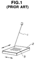
- Fig. 1 is a view illustrating steps of a first prior art diffraction grating fabricating method.
- Fig. 2 is a view illustrating steps of a second prior art diffraction grating fabricating method.
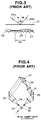
- Fig. 3 is a view illustrating steps of a third prior art diffraction grating fabricating method.
- Fig. 4 is a view illustrating steps of a fourth prior art diffraction grating fabricating method.
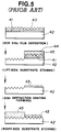
- Fig. 5 is a view illustrating steps of a fifth prior art diffraction grating fabricating method.
- Figs. 6A-6M are views illustrating steps of an embodiment according to the present invention.
- Figs. 6A-6M respectively show steps of an embodiment of a diffraction grating producing method according to the present invention.
- a semiconductor substrate 61 is cleaned by a surface active agent, and then is cleaned by ultrasonic means two or three times using an organic solvent. Thereafter, the substrate 61 is heat-treated at a temperature of 200°C for thirty (30) minutes by drying it with an N2 blow. Then, a photoresist layer 62 for a two-beam interference exposure is formed on the substrate 61 by coating a photoresist made by diluting to a desired concentration over the substrate 62.
- This substrate 61 with the photoresist 62 is soft-baked at a temperature of 115 °C for forty five (45) seconds
- hexamethyldisilazane (trade name HMDS : produced by Tisso Inc.) that is a contact-enhancing agent may be spin-coated on the substrate 61 and the heat-treatment at a temperature of 150°C may be performed for ten (10) minutes.
- a composition of the photoresist for interference exposure is as follows: Polyvinylphenol (its average molecular weight is 15,000 in terms of a polystyrene reduction) and a mixture of naphtoquinonediazide-5-sulfonylchrolide and ester compound of 2,3,4 trihydroxybenzophenon (photosensitive agent) (weight ration 3:1) are dissolved into ethylcellosolveaceto, and this is filtered by a membrane filter of 0.2 ⁇ m made of Teflon (trade name).
- the thickness of the photoresist 62 is properly set to 800 ⁇ -1000 ⁇ or less than 3000 ⁇ (see Fig. 6A).
- the photoresist layer 62 is then developed with a developer of alkali group.
- a resist pattern (diffraction grating) 63 is formed corresponding to a photosensitivity degree resulting from the intensity distribution of interference fringes caused by the interference exposure (see Fig. 6B).
- the diffraction grating 63 has a rectangular or square shape.
- a specific photoresist is used, and after the two-wave interference exposure is performed using the He-Cd laser or the like, the development is conducted using a specific developer.
- a base resin that is as transparent as possible to the wavelength of the exposure light (i.e., its absorption factor thereto is as small as possible).
- Polyvinylphenol or its copolymer with an appropriate different monomer or monomers is desirably used. For example, styrene, paramethylstyrene, ⁇ -methylstyrene, derivatives of styrene can be enumerated.
- quinonediazide group such as a mixture of 1,2 naphtoquinonediazide-5-sulfonylchrolide, 1,2 naphtoquinonediazide-4-sulfonylchrolide or the like mixed with compound having no carbonyl group such as bisphenol A exhibiting no absorption to the wavelength of the exposure light is desirably used.
- ethyllactate ethyl acetate cellosolve
- propylene glycol ⁇ monomethyl ether acetate lactic acid ethyl, diacetone alcohol, cyclohexanone or the like
- an alkaline solution such as trimethyl hydroxy ethyl, ammonium hydroxide, sodium hydroxide, potassium hydroxide, tetramethyl ammonium and hydraxide solution is desirably used.
- a photoresist layer 65 (trade name RD-2000N : produced by Hitachi Kasei Inc.), for example, is coated over all of the semiconductor substrate 61 to form a phase region (reference pitch region) and a phase shift region (reverse pitch region). This is then dried at a temperature of 80 °C for twenty (20) minutes (see Fig. 6D). The thickness of the photoresist layer 65 is properly set to 1.5 ⁇ m-2.0 ⁇ m.
- a mask exposure is conducted by a photomask 66 using an ordinary photolithographic technique (see Fig. 6E). Then, development and cleaning are successively performed using a specific developer for the photoresist layer 65 (trade name RD-developer : produced by Hitachi Kasei Inc.) and a specific cleaning liquid (trade name RD-postrinse).
- a striped pattern 67 is formed on the semiconductor substrate 61 (see Fig. 6F).
- the striped pattern 67 functions as both of an etching protection layer for the phase shift region at the time of etching the phase region and a lift-off layer for forming a protection layer of the phase region.
- Unnecessary metal titanium is then etched using, for example, a buffered hydrofluoric acid for the purpose of performing the etching of the semiconductor substrate 61 in the phase region (see Fig. 6G). Only the diffraction grating pattern 63 of photoresist remains in the phase region .
- the semiconductor substrate 61 is then etched using, for example, the reactive ion beam etching (RIBE) of chrolide series with the diffraction grating pattern 63 of photoresist on the phase region used as an etching mask (Fig. 6H). At this time, the phase shift region is covered by the etching protection layer of the striped pattern 67.
- RIBE reactive ion beam etching
- a semiconductor diffraction grating 68 is obtained on the phase region of the semiconductor substrate 61 by removing the above-discussed etching mask in a dry or wet manner (see Fig. 6I).
- Metal titanium for example, is then deposited over all of the substrate 61 to form an etching mask layer 69 for the semiconductor diffraction grating 68, using the electron beam deposition method.
- Conditions thereof are such that an arrival vacuum degree is less than 2.0 ⁇ 10 ⁇ 6 Torr, a substrate temperature is a room temperature, an acceleration voltage is 10 kV and an emission current is 95 mA. Under these conditions, a deposition rate is 2 ⁇ /sec.
- the film thickness of the metal titanium 69 is properly set to 2600 ⁇ -3000 ⁇ (see Fig. 6J).
- a self-alignment using the striped pattern 67 without a mask alignment is conducted to form the phase region and the phase shift region.
- the reverse mask layer 64 of metal titanium is then formed by a lift-off method in order to form a diffraction grating in the phase shift region.
- the photoresist of the striped pattern 67 which becomes unnecessary together with the diffraction grating pattern 63 of photoresist and the metal titanium 69 for the lift-off which is deposited in the previous step are simultaneously lifted off.
- Conditions at this time are such that a remover liquid (trade name Microposit Remover 140 : produce by Shipley Inc.) is heated to 80°C-90 °C by a hot plate and the lift-off is then conducted by means of ultrasonic cleaning.
- a remover liquid trade name Microposit Remover 140 : produce by Shipley Inc.
- the semiconductor substrate 61 is then etched using, for example, the reactive ion beam etching (RIBE) of chrolide series with the reverse mask layer 64 on the phase shift region used as an etching mask.
- RIBE reactive ion beam etching
- a diffraction grating 70 whose pitch is reverse to that on the phase region is obtained.
- the semiconductor diffraction grating 68 on the phase region is protected by the etching mask layer 69 of metal titanium (see Fig. 6L).
- Unnecessary metal titanium of the reverse mask layer 64 and the etching mask layer 69 are then removed using, for example, buffered hydrofluoric acid. As a result, a phase-shifted type diffraction grating 71 is obtained on the semiconductor substrate 61 (see Fig. 6M).
- the wavelength and kind of the ultraviolet laser for interference exposure may be determined depending on specifications (pitch, depth and so forth) of the phase-shifted diffraction grating.
- the semiconductor substrate is used in the above embodiment, glass, optical glass or the like may be utilized.
- the photoresist is used as the film material 62, an oxide film such as SiO2 film, a nitride film such as Si3N4 film or other metal layers, for example, may be used as long as the diffraction grating pattern having the reference period or pitch can be formed.
- the kind and type (positive or negative) of the photoresist may be determined according to the specifications of the phase-shifted diffraction grating.
- the metal titanium is used as the reverse mask layer 64 and the etching mask layer 69, but an oxide layer such as SiO2 film, a nitride film such as Si3N4 film or other metal layers, for example, may be used. This material may be determined depending on a ratio of layers, a selective ratio or difference in the etching rates between etched materials at the time of etching and the specisications of the phase-shifted diffraction grating.
- the electron beam deposition method is used as a method for forming the metal titanium of the reverse mask layer 64 and the etching mask layer 69
- a sputtering deposition method or a resistance heating deposition method may be used depending on the specifications and the materials.
- the chrolide gas RIBE of a dry method is used for performing the etching of the semiconductor substrate 61, kinds of the etching and the gas are not limited. They may be determined depending on the specifications, materials, selective ratio and the like.
- the following advantages can be obtained, compared with the prior art methods of fabricating the phase-shifted type diffraction grating:
- phase-shifted diffraction grating can be readily fabricated, a diffraction grating having a deep groove can be produced since the etching mask layer can be thickened, the pattern accuracy and the shape stability can be improved, and the transient area can be shortened.
- a phase-shifted diffraction grating for devices such as semiconductor lasers is produced by forming a first diffraction grating pattern of a first material having a reference pitch on a substrate.
- the substrate is then coated with a second material on both the first material and an exposed portion of the substrate in a region where a second diffraction grating having a pitch which is the reverse of the reference pitch of the first diffraction grating pattern is to be formed.
- the first material is removed by lift off to obtain the second diffraction grating pattern on the second diffraction grating region.
- the substrate is etched using the first diffraction grating as an etching mask to form the first diffraction grating and then the substrate is etched with the second diffraction grating pattern as an etching mask to obtain a second diffraction grating continuous with the first diffraction grating.
- the first diffraction grating pattern may have a rectangular or square shape to stably and accurately remove the first material by lift-off and the boundary between the first and second diffraction gratings can be stably and accurately defined by self-alignment.
Landscapes
- Physics & Mathematics (AREA)
- Engineering & Computer Science (AREA)
- Manufacturing & Machinery (AREA)
- General Physics & Mathematics (AREA)
- Optics & Photonics (AREA)
- Diffracting Gratings Or Hologram Optical Elements (AREA)
- Semiconductor Lasers (AREA)
Abstract
Description
- This invention relates to a method for producing a diffraction grating, and more particularly, to a method for producing a phase-shifted diffraction grating such as λ/4-shifted diffraction grating for use in various devices such as filters and semiconductor lasers, typically distributed feedback (DFB) type lasers.
- Diffraction gratings have been used in opto-electronic fields as various optical circuit devices such as filters, optical couplers, distributed feedback (DFB) type lasers, distributed Bragg reflection (DBR) type lasers and the like. In particular, DFB and DBR lasers using diffraction gratings as resonators for lasers have been studied and developed for their stable dynamic single mode characteristics that make oscillation wavelengths stable even if the lasere are directly modulated.
- On the other hand, λ/4-shifted DFB lasers with phase-shifted diffraction gratings have been developed several years ago to improve the oscillation singularity of these lasers (see Japanese Patent Laid-open No. 62-262004). The λ/4-shifted DFB laser oscillates in a single longitudinal mode which is equal to a Bragg wavelength thereof, so that a previous problem of oscillation occuring in two longitudinal modes in conventional lasers has almost been solved.
- The following methods have been used in fabricating structures that achieve the λ/4-shift effect, when classified roughly.
- (1) The period or phase of a diffraction grating is reversed halfway thereof, and its phase is shifted by λ/4 or quarter wave.
- (2) The phase of light is equivalently shifted by partially adjusting its propagation constant by means of a change in the width of a diffraction grating and the like.
- Method (1) can be realized comparatively readily. In the method (1), ordinary diffraction grating producing techniques can be adopted.
- Further, the following methods are known to produce a phase-shifted type diffraction grating, roughly classified.
- (1) An electron beam direct depicting method is shown in Fig. 1. An
electron beam 1 is scanned in directions of arrows on asubstrate 2 to form a diffraction grating 3. - (2) An interference exposure method in which both of high-resolution positive and negative photoresists of novolac series are used and an intermediate layer is provided to prevent mixing between these photoresists as shown in Fig. 2.
Initially, a 70 nm-thick negative photoresist (ONNR-20) 12, a 60 nm-thick cyclised polyisoprene (OBC) 13 and a 0.5 µm-thick positive photoresist (MP-1400) ofAZ layer 14 are spin-coated successively onto an InP substrate 11. Next, striped patterns of positive photoresist are generated by photolithography. Using these patterns as a mask, thecyclised polyisoprene 13 and thenegative photoresist 12 are etched off by an H₂SO₄+H₂O₂ solution. Then, negative photoresist line patterns covered with thecyclised polyisoprene 13 are obtained by removing thepositive photoresist 14 by means of its developer. After this, a positive AZphotoresist layer 15 for interference exposure and a 70 nm-thick polyvinyl alcohol (PVA) 16 are spin-coated. The PVA 16 enhances the photosensitivity of thenegative photoresist 12 because oxygen in air does not penetrate this thin film. Using this technique, almost the same photosensitivity is obtained for the positive andnegative photoresists photoresists - (3) An interference exposure method using a
contact mask 21 of quartz as a phase mask is shown in Fig. 3. Thecontact mask 21 is made of a transparent material whose thickness is varied according to its region. In Fig. 3,reference numeral 22 designates a substrate surface,reference numeral 23 designates interference fringes,reference numeral 24 designates a laser resonator,reference numeral 25 designates a transient area andreference numerals 26a and 26b designate laser light beams entering thecontact mask 21 at incident angles ϑL and ϑR, respectively. In this connection, see M. SHIRASAKI et al, " λ/4 shifted DFB-LD corrugation formed by a novel spatial phase modulating mask", OQE 85-60, FUJITSU LABORATORIES LTD., pp. 57-64. - (4) An interference exposure method using a projected image of a phase mask or a
phase plate 31 is shown in Fig. 4. In Fig. 4,reference numeral 32 designates a beam splitter,reference numeral 33 designates a spatial filter,reference numeral 34 designates a collimating lens,reference numeral 35 designates a plane mirror,reference numeral 36 designates a lens system having a common focal point andreference numeral 37 designates a sample surface. In this connection, see S. TSUJI et al, "phase-shift grating for single mode DFB lasers fabricated by phase projection type holography", Informal Papers of Electronics Communication Academy Semiconductor-Material Division Grand Meeting, 1985, p. 127. - (5) A method in which a conventional interference exposure method is used and a part is reversely transferred onto a substrate using SiNx layer formed by an electron cyclotron resonance-chemical vapor deposition (ECR-CVD) method is shown in Fig. 5. In Fig. 5, initially, a diluted positive photoresist (MP-1400) 41 is spin-coated onto an
InP substrate 42. Then an ordinary holographic exposure with an He-Cd laser beam (325 nm) and development are performed to make aphotoresist corrugation 41 with a period of 240 nm. The SiNx film 43 is deposited onto it by ECR-CVD at room temperature. After spin-coating aphotoresist 44 again, striped patterns parallel to thecorrugation 41 are formed by conventional photolithography. In this procedure the SiNx film 43 prevents thephotoresist corrugation 41 from being dissolved into the developer. Using these striped patterns as a mask, etching of the SiNx film 43 is performed. In the region where the SiNx film is taken off, theInP substrate 42 is etched using thephotoresist corrugation 41 as a mask to fabricate a diffraction grating on theInP substrate 42. Then thephotoresist 44 covering the SiNx film 43 is removed. In the next step, an SiNx film corrugation 43, whose phase is reverse to the photoresist corrugation, is produced in the region where the SiNx film have been covered and not etched. In this process a unique characteristic of the ECR-CVD SiNx film 43 is utilised. The SiNx film 43 deposited on thephotoresist 41 is etched by a buffered HF solution (BHF) at a higher rate than on the flat substrate. By optimising the etching condition, this difference in etching rates makes it possible to not etch only the parts of the SiNx film 43 on the flat substrates. After removing the photoresist and covering the previously formed grating on thesubstrate 42 withphotoresist 45, theInP substrate 42 is etched using the SiNx film corrugation 43 as a mask. With this process, a quarter-wave-shifted diffraction grating is fabricated on theInP substrate 42. In this connection, see H. SUGIMOTO et al, "NOVEL FABRICATION METHOD OF QUARTER-WAVE-SHIFTED GRATINGS USING ECR-CVD SiNx FILMS", Electron. Lett., 19th November 1987, Vol. 23, No. 24, pp. 1260-1261. - However, the above-discussed methods for fabricating a phase-shifted type diffraction grating have the following disadvantages:
- In the first method (Fig. 1), while a fine pattern can be directly depicted on the
substrate 2 with high accuracy, a proximity effect appears between adjacent gratings depending on the relationship between the grating interval (e.g., 0.25 µm) and the electron beam diameter (e.g., 0.1 µm) and a backscattering due to the electron beam scattering on a substrate surface having a photoresist coated thereon. As a result, it is difficult to form thediffraction grating 3 having a pitch of less than 0.3 µm on a thick resist or a thick substrate. Further, its throughput and yield are inevitably reduced. - In the second method (Fig. 2), a complicated fabrication process is needed. That is, differences in appropriate exposure and development conditions for positive and
negative photoresists - In the third method (Fig. 3), the phase
transient area 25 of thelaser resonator 24 is widened due to a Fresnel diffraction oflight beams 26a and 26b applied to cause the interference exposure unless the contact between thecontact mask 21 and the photoresist layer coated on the substrate'ssurface 22 is sufficient. - In the fourth method (Fig. 4), the
phase shifter 31 of a quartz plate having a step corresponding to a phase shift is disposed in the optical system, and thisphase shifter 31 is irradiated with a slant projected light beam. The slant projection is required since the image must be formed on thesample surface 37 to which two beams are slantedly applied. As a result, abberations occur on thesample surface 37, and hence an area on which the diffraction grating can be formed is limited. - In the fifth method (Fig. 5), it is difficult to control the etching conditions of the SiNx film 43 on the resist 41 and the
substrate 42. Moreover, two etchings are performed for thesubstrate 42, and the control of the conditions is difficult. Thus, the shape of the diffraction grating is likely to be irregular, and the accuracies of depth and size thereof are lowered. - It is an object of the present invention to provide a method of fabricating a diffraction grating having a shifted phase on a common substrate with good accuracy and stability.
- According to one aspect of the present invention, there are the steps of: forming a first diffraction grating pattern of a first material having a reference pitch on a substrate, coating a second material different from the first material on both of the first material and an exposed portion of the substrate in a region where a second diffraction grating pattern having a pitch reverse to the reference pitch of the first diffraction grating pattern of the first material is to be formed, removing the first material by a lift-off method to obtain the second diffraction grating pattern of the second material having the reverse pitch in the region on the substrate, etching the substrate with the first diffraction grating pattern of the first material having the reference pitch used as an etching mask to form a first diffraction grating and etching the substrate with the second diffraction grating pattern of the second material having the reverse pitch used as an etching mask to obtain a second diffraction grating continuous to the first diffraction grating and hence a phase-shifted diffraction grating.
- According to another aspect of the present invention, there are the steps of: forming a first diffraction grating pattern of a first material having a reference pitch on a substrate, coating a second material different from the first material on both of the first material and an exposed portion of the substrate in a region where a second diffraction grating pattern having a pitch reverse to the reference pitch of the first diffraction grating pattern of the first material is to be formed, forming a first etching protection layer on the region where the second diffraction grating pattern is to be formed, etching the substrate with the first diffraction grating pattern of the first material having the reference pitch used as an etching mask to form a first diffraction grating, forming a second etching protection layer on a region where the first diffraction grating is formed, removing the first material by a lift-off method to obtain the second diffraction grating pattern of the second material having the reverse pitch, and etching the substrate with the second diffraction grating pattern of the second material having the reverse pitch used as an etching mask to form a second diffraction grating continuous to the first diffraction grating and hence a phase-shifted diffraction grating.
- In the method of fabricating a phase-shifted diffraction grating of the present invention, the first diffraction grating pattern is preferebly shaped into a rectangular or square shape in order to stably and accurately perform the first material removing step by the lift-off method. Further, a boundary between the first and second diffraction gratings can be stably and accurately defined in a self-alignment manner, i.e., automatically without using mask alignment.
- These advantages and others will be more readily understood in connection with the following detailed description, claims and drawings.
- Fig. 1 is a view illustrating steps of a first prior art diffraction grating fabricating method.
- Fig. 2 is a view illustrating steps of a second prior art diffraction grating fabricating method.
- Fig. 3 is a view illustrating steps of a third prior art diffraction grating fabricating method.
- Fig. 4 is a view illustrating steps of a fourth prior art diffraction grating fabricating method.
- Fig. 5 is a view illustrating steps of a fifth prior art diffraction grating fabricating method.
- Figs. 6A-6M are views illustrating steps of an embodiment according to the present invention.
- Figs. 6A-6M respectively show steps of an embodiment of a diffraction grating producing method according to the present invention.
- Initially, a
semiconductor substrate 61 is cleaned by a surface active agent, and then is cleaned by ultrasonic means two or three times using an organic solvent. Thereafter, thesubstrate 61 is heat-treated at a temperature of 200°C for thirty (30) minutes by drying it with an N₂ blow. Then, aphotoresist layer 62 for a two-beam interference exposure is formed on thesubstrate 61 by coating a photoresist made by diluting to a desired concentration over thesubstrate 62. Thissubstrate 61 with thephotoresist 62 is soft-baked at a temperature of 115 °C for forty five (45) seconds Before forming thephotoresist layer 62, hexamethyldisilazane (trade name HMDS : produced by Tisso Inc.) that is a contact-enhancing agent may be spin-coated on thesubstrate 61 and the heat-treatment at a temperature of 150°C may be performed for ten (10) minutes. - In this embodiment, a composition of the photoresist for interference exposure is as follows: Polyvinylphenol (its average molecular weight is 15,000 in terms of a polystyrene reduction) and a mixture of naphtoquinonediazide-5-sulfonylchrolide and ester compound of 2,3,4 trihydroxybenzophenon (photosensitive agent) (weight ration 3:1) are dissolved into ethylcellosolveaceto, and this is filtered by a membrane filter of 0.2 µm made of Teflon (trade name).
- The thickness of the
photoresist 62 is properly set to 800Å -1000 Å or less than 3000Å (see Fig. 6A). - The
photoresist layer 62 is then exposed to two light beams respectively entering at incident angles corresponding to a desired period or pitch, according to the two-beam interference exposure method using an He-Cd laser (wavelength: λ = 325 nm). Thephotoresist layer 62 is then developed with a developer of alkali group. As a result, a resist pattern (diffraction grating) 63 is formed corresponding to a photosensitivity degree resulting from the intensity distribution of interference fringes caused by the interference exposure (see Fig. 6B). Thediffraction grating 63 has a rectangular or square shape. - In the process of fabricating the
diffraction grating 63 of a rectangular or square shape, a specific photoresist is used, and after the two-wave interference exposure is performed using the He-Cd laser or the like, the development is conducted using a specific developer. For the photoresist, it is desirable to use a base resin that is as transparent as possible to the wavelength of the exposure light (i.e., its absorption factor thereto is as small as possible). Polyvinylphenol or its copolymer with an appropriate different monomer or monomers is desirably used. For example, styrene, paramethylstyrene, α-methylstyrene, derivatives of styrene can be enumerated. - For a photosensitive agent of the photoresist, quinonediazide group such as a mixture of 1,2 naphtoquinonediazide-5-sulfonylchrolide, 1,2 naphtoquinonediazide-4-sulfonylchrolide or the like mixed with compound having no carbonyl group such as bisphenol A exhibiting no absorption to the wavelength of the exposure light is desirably used.
- For a principal solvent, ethyllactate, ethyl acetate cellosolve, propylene glycol·monomethyl ether acetate, lactic acid ethyl, diacetone alcohol, cyclohexanone or the like can be enumerated. For the developer, an alkaline solution such as trimethyl hydroxy ethyl, ammonium hydroxide, sodium hydroxide, potassium hydroxide, tetramethyl ammonium and hydraxide solution is desirably used.
- Next, a
reverse mask layer 64 for phase shifting made of, for example, metal titanium is deposited using an electron beam deposition method. Conditions thereof are such that an arrival vacuum degree is 2.0 × 10⁻⁶ Torr, a substrate temperature is equal to a room temperature, an acceleration voltage is 10 kV and an emission current is 95 mA. Under these conditions, a deposition rate is 2 Å/sec. Here, the film thickness of themetal titanium 64 is properly set to 100 Å - 200Å (see Fig. 6C). The thickness of thephotoresist pattern 63 should be larger than two times that of themetal titanium 64. - Next, a photoresist layer 65 (trade name RD-2000N : produced by Hitachi Kasei Inc.), for example, is coated over all of the
semiconductor substrate 61 to form a phase region (reference pitch region) and a phase shift region (reverse pitch region). This is then dried at a temperature of 80 °C for twenty (20) minutes (see Fig. 6D). The thickness of thephotoresist layer 65 is properly set to 1.5 µm-2.0 µm. - A mask exposure is conducted by a
photomask 66 using an ordinary photolithographic technique (see Fig. 6E). Then, development and cleaning are successively performed using a specific developer for the photoresist layer 65 (trade name RD-developer : produced by Hitachi Kasei Inc.) and a specific cleaning liquid (trade name RD-postrinse). Astriped pattern 67 is formed on the semiconductor substrate 61 (see Fig. 6F). Thestriped pattern 67 functions as both of an etching protection layer for the phase shift region at the time of etching the phase region and a lift-off layer for forming a protection layer of the phase region. - Unnecessary metal titanium is then etched using, for example, a buffered hydrofluoric acid for the purpose of performing the etching of the
semiconductor substrate 61 in the phase region (see Fig. 6G). Only thediffraction grating pattern 63 of photoresist remains in the phase region . - The
semiconductor substrate 61 is then etched using, for example, the reactive ion beam etching (RIBE) of chrolide series with thediffraction grating pattern 63 of photoresist on the phase region used as an etching mask (Fig. 6H). At this time, the phase shift region is covered by the etching protection layer of thestriped pattern 67. - A
semiconductor diffraction grating 68 is obtained on the phase region of thesemiconductor substrate 61 by removing the above-discussed etching mask in a dry or wet manner (see Fig. 6I). - Metal titanium, for example, is then deposited over all of the
substrate 61 to form anetching mask layer 69 for thesemiconductor diffraction grating 68, using the electron beam deposition method. Conditions thereof are such that an arrival vacuum degree is less than 2.0 × 10⁻⁶ Torr, a substrate temperature is a room temperature, an acceleration voltage is 10 kV and an emission current is 95 mA. Under these conditions, a deposition rate is 2 Å/sec. Here, the film thickness of themetal titanium 69 is properly set to 2600Å -3000Å (see Fig. 6J). A self-alignment using thestriped pattern 67 without a mask alignment is conducted to form the phase region and the phase shift region. - The
reverse mask layer 64 of metal titanium is then formed by a lift-off method in order to form a diffraction grating in the phase shift region. At this time, the photoresist of thestriped pattern 67 which becomes unnecessary together with thediffraction grating pattern 63 of photoresist and themetal titanium 69 for the lift-off which is deposited in the previous step are simultaneously lifted off. Conditions at this time are such that a remover liquid (trade name Microposit Remover 140 : produce by Shipley Inc.) is heated to 80°C-90 °C by a hot plate and the lift-off is then conducted by means of ultrasonic cleaning. Thus, thesemiconductor diffraction grating 68 on the phase region is protected by themetal titanium 69, and thereverse mask layer 64 of metal titanium is formed on the phase shift region (see Fig. 6K). - The
semiconductor substrate 61 is then etched using, for example, the reactive ion beam etching (RIBE) of chrolide series with thereverse mask layer 64 on the phase shift region used as an etching mask. Thus, a diffraction grating 70 whose pitch is reverse to that on the phase region is obtained. At this time, thesemiconductor diffraction grating 68 on the phase region is protected by theetching mask layer 69 of metal titanium (see Fig. 6L). - Unnecessary metal titanium of the
reverse mask layer 64 and theetching mask layer 69 are then removed using, for example, buffered hydrofluoric acid. As a result, a phase-shifted type diffraction grating 71 is obtained on the semiconductor substrate 61 (see Fig. 6M). - In the above-discussed embodiment, various modifications are possible in respective portions or means. For example, the wavelength and kind of the ultraviolet laser for interference exposure may be determined depending on specifications (pitch, depth and so forth) of the phase-shifted diffraction grating. Further, while the semiconductor substrate is used in the above embodiment, glass, optical glass or the like may be utilized. Furthermore, while the photoresist is used as the
film material 62, an oxide film such as SiO₂ film, a nitride film such as Si₃N₄ film or other metal layers, for example, may be used as long as the diffraction grating pattern having the reference period or pitch can be formed. - While the negative type photoresist RD-2000N is used as the
photoresist layer 65 that is utilized as the lift-off layer, the kind and type (positive or negative) of the photoresist may be determined according to the specifications of the phase-shifted diffraction grating. Further, the metal titanium is used as thereverse mask layer 64 and theetching mask layer 69, but an oxide layer such as SiO₂ film, a nitride film such as Si₃N₄ film or other metal layers, for example, may be used. This material may be determined depending on a ratio of layers, a selective ratio or difference in the etching rates between etched materials at the time of etching and the specisications of the phase-shifted diffraction grating. - Further, while the electron beam deposition method is used as a method for forming the metal titanium of the
reverse mask layer 64 and theetching mask layer 69, a sputtering deposition method or a resistance heating deposition method may be used depending on the specifications and the materials. Furthermore, the chrolide gas RIBE of a dry method is used for performing the etching of thesemiconductor substrate 61, kinds of the etching and the gas are not limited. They may be determined depending on the specifications, materials, selective ratio and the like. - According to the present invention, the following advantages can be obtained, compared with the prior art methods of fabricating the phase-shifted type diffraction grating:
- The phase-shifted diffraction grating can be readily fabricated, a diffraction grating having a deep groove can be produced since the etching mask layer can be thickened, the pattern accuracy and the shape stability can be improved, and the transient area can be shortened.
- While the present invention has been described with respect to what is presently considered to be the preferred embodiment, it is understood that the invention is not limited to the disclosed embodiment. The present invention is intended to cover various modifications and equivalent arrangements included within the spirit and scope of the appended claims.
- A phase-shifted diffraction grating for devices such as semiconductor lasers is produced by forming a first diffraction grating pattern of a first material having a reference pitch on a substrate. The substrate is then coated with a second material on both the first material and an exposed portion of the substrate in a region where a second diffraction grating having a pitch which is the reverse of the reference pitch of the first diffraction grating pattern is to be formed. The first material is removed by lift off to obtain the second diffraction grating pattern on the second diffraction grating region. The substrate is etched using the first diffraction grating as an etching mask to form the first diffraction grating and then the substrate is etched with the second diffraction grating pattern as an etching mask to obtain a second diffraction grating continuous with the first diffraction grating. The first diffraction grating pattern may have a rectangular or square shape to stably and accurately remove the first material by lift-off and the boundary between the first and second diffraction gratings can be stably and accurately defined by self-alignment.
Claims (24)
- A method for producing a phase-shifted diffraction grating comprising the steps of:
forming a first diffraction grating pattern of a first material having a reference pitch on a substrate;
coating a second material different from said first material on both of said first material and an exposed portion of said substrate in a region where a second diffraction grating pattern having a pitch reverse to the reference pitch of said first diffraction grating pattern of said first material is to be formed;
removing said first material by a lift-off method to obtain said second diffraction grating pattern of said second material having the reverse pitch in said region on said substrate;
etching said substrate with said first diffraction grating pattern of said first material having the reference pitch used as an etching mask to form a first diffraction grating; and
etching said substrate with said second diffraction grating pattern of said second material having the reverse pitch used as an etching mask to obtain a second diffraction grating continuous with said first diffraction grating. - A method for producing a phase-shifted diffraction grating according to Claim 1, further comprising a step of forming a first etching protection layer on said region where said second diffraction grating is to be formed.
- A method for producing a phase-shifted diffraction grating according to Claim 1, further comprising a step of forming a second etching protection layer on a region where said first diffraction grating is formed.
- A method for producing a phase-shifted diffraction grating according to Claim 3, wherein said removing step and said second etching protection layer forming step are simultaneously performed while forming a boundary between said first and second diffraction gratings.
- A method for producing a phase-shifted diffraction grating according to Claim 1, wherein a boundary between said first and second diffraction gratings is formed in a self-alignment manner.
- A method for producing a phase-shifted diffraction grating according to Claim 1, wherein said first diffraction grating pattern has a rectangular shape.
- A method for producing a phase-shifted diffraction grating according to Claim 1, wherein said first diffraction grating pattern forming step comprises: coating a photoresist on said substrate, performing a two-beam interference exposure using a laser for interference exposure and developing said photoresist with an alkaline solution.
- A method for producing a phase-shifted diffraction grating according to Claim 7, wherein said photoresist comprises a base resin of polyvinylphenol or its copolymer with different monomer and a photosensitive agent of quinonediazide group.
- A method for producing a phase-shifted diffraction grating according to Claim 7, wherein the thickness of said photoresist is less than 3000Å.
- A method for producing a phase-shifted diffraction grating according to Claim 1, wherein said substrate comprises a semiconductor.
- A method for producing a phase-shifted diffraction grating according to Claim 1, wherein said substrate comprises a glass.
- A method for producing a phase-shifted diffraction grating according to Claim 1, wherein said substrate comprises an optical glass.
- A method for producing a phase-shifted diffraction grating according to Claim 1, wherein said second material comprises titanium.
- A method for producing a phase-shifted diffraction grating according to Claim 1, wherein the thickness of said second material is less than one half the thickness of said first material.
- A method for producing a phase-shifted diffraction grating according to Claim 2, wherein said first etching protection layer comprises a photoresist.
- A method for producing a phase-shifted diffraction grating according to Claim 2, wherein the thickness of said first etching protection layer is in a range between 1.5 µm and 2.0 µm.
- A method for producing a phase-shifted diffraction grating according to Claim 3, wherein said second etching protection layer comprises titanium.
- A method for producing a phase-shifted diffraction grating according to Claim 3, wherein the thickness of said second etching protection layer is in a range between 2000Å and 3000 Å.
- A method for producing a phase-shifted diffraction grating, said method comprising the steps of:
forming a first diffraction grating pattern of a first material having a reference pitch on a substrate;
coating a second material different from said first material on both of said first material and an exposed portion of said substrate in a region where a second diffraction grating pattern having a pitch reverse to the reference pitch of said first diffraction grating pattern of said first material is to be formed:
forming a first etching protection layer on the region where said second diffraction grating pattern is to be formed;
etching said substrate with said first diffraction grating pattern of said first material having the reference pitch used as an etching mask to form a first diffraction grating;
forming a second etching protection layer on a region where said first diffraction grating is formed;
removing said first material by a lift-off method to obtain said second diffraction grating pattern of said second material having the reverse pitch; and
etching said substrate with said second diffraction grating pattern of said second material having the reverse pitch used as an etching mask to form a second diffraction grating continuous to said first diffraction grating. - A method for producing a phase-shifted diffraction grating according to Claim 19, wherein said removing step and said second etching protection layer forming step are simultaneously performed while forming a boundary between said first and second diffraction gratings.
- A method for producing a phase-shifted diffraction grating according to Claim 19, wherein a boundary between said first and second diffraction gratings is formed in a self-alignment manner.
- A method for producing a phase-shifted diffraction grating according to Claim 19, wherein said first diffraction grating pattern has a rectangular shape.
- A method for producing a phase-shifted diffraction grating according to Claim 19, wherein said first diffraction grating pattern forming step comprises: coating a photoresist on said substrate, performing a two-beam interference exposure using a laser for interference exposure and developing said photoresist with an alkaline solution.
- A method for producing a phase-shifted diffraction grating according to Claim 23, wherein said photoresist comprises a base resin of polyvinylphenol or its copolymer with different monomer and a photosensitive agent of quinonediazide group.
Applications Claiming Priority (4)
| Application Number | Priority Date | Filing Date | Title |
|---|---|---|---|
| JP13822991A JPH04337702A (en) | 1991-05-14 | 1991-05-14 | Formation of diffraction grating |
| JP138229/91 | 1991-05-14 | ||
| JP13822891A JPH04337701A (en) | 1991-05-14 | 1991-05-14 | Formation of diffraction grating |
| JP138228/91 | 1991-05-14 |
Publications (2)
| Publication Number | Publication Date |
|---|---|
| EP0513755A2 true EP0513755A2 (en) | 1992-11-19 |
| EP0513755A3 EP0513755A3 (en) | 1994-05-18 |
Family
ID=26471336
Family Applications (1)
| Application Number | Title | Priority Date | Filing Date |
|---|---|---|---|
| EP19920108066 Withdrawn EP0513755A3 (en) | 1991-05-14 | 1992-05-13 | A method for producing a diffraction grating |
Country Status (2)
| Country | Link |
|---|---|
| US (1) | US5225039A (en) |
| EP (1) | EP0513755A3 (en) |
Cited By (6)
| Publication number | Priority date | Publication date | Assignee | Title |
|---|---|---|---|---|
| DE4233500A1 (en) * | 1992-10-06 | 1994-04-07 | Ant Nachrichtentech | Optical waveguide for the continuous phase shift of the DFB grating period for optoelectronic components based on DFB grating fields with a constant grating period |
| EP0632297A1 (en) * | 1993-07-02 | 1995-01-04 | Xerox Corporation | Phase control in a binary diffractive optical element by spatial displacement |
| EP0683404A1 (en) * | 1994-04-08 | 1995-11-22 | Enea Ente Per Le Nuove Tecnologie, L'energia E L'ambiente | Method and apparatus for producing diffraction gratings by machine forming in a fast operation cycle |
| EP1316993A1 (en) * | 2001-11-29 | 2003-06-04 | Denselight Semiconductors Pte Ltd. | Differential etching of semiconductors |
| GB2417730A (en) * | 2004-08-06 | 2006-03-08 | Agilent Technologies Inc | Method to fabricate diffractive optics |
| CN111033324A (en) * | 2017-06-02 | 2020-04-17 | 迪斯帕列斯有限公司 | Method of manufacturing a highly modulated optical diffraction grating |
Families Citing this family (18)
| Publication number | Priority date | Publication date | Assignee | Title |
|---|---|---|---|---|
| JP2738623B2 (en) * | 1992-04-23 | 1998-04-08 | 三菱電機株式会社 | Method of forming diffraction grating |
| JP2546135B2 (en) * | 1993-05-31 | 1996-10-23 | 日本電気株式会社 | Method of forming semiconductor fine shape, method of manufacturing InP diffraction grating, and method of manufacturing distributed feedback laser |
| US5417799A (en) * | 1993-09-20 | 1995-05-23 | Hughes Aircraft Company | Reactive ion etching of gratings and cross gratings structures |
| JP3366441B2 (en) * | 1994-06-21 | 2003-01-14 | 三菱電機株式会社 | Method of manufacturing λ / 4 shift diffraction grating |
| KR100424774B1 (en) * | 1998-07-22 | 2004-05-17 | 삼성전자주식회사 | Mask for forming selection area diffraction grating and growing selection area and method of manufacturing semiconductor device using the same |
| US6072579A (en) * | 1998-08-27 | 2000-06-06 | Ricoh Company, Ltd. | Optical pickup apparatus having improved holographic optical element and photodetector |
| JP3797462B2 (en) * | 1999-07-08 | 2006-07-19 | 富士写真フイルム株式会社 | Diffraction grating manufacturing method |
| US6510263B1 (en) * | 2000-01-27 | 2003-01-21 | Unaxis Balzers Aktiengesellschaft | Waveguide plate and process for its production and microtitre plate |
| US6961490B2 (en) * | 2000-01-27 | 2005-11-01 | Unaxis-Balzers Aktiengesellschaft | Waveguide plate and process for its production and microtitre plate |
| US6904201B1 (en) * | 2001-05-09 | 2005-06-07 | Intel Corporation | Phase-controlled fiber Bragg gratings and manufacturing methods |
| US6869754B2 (en) * | 2001-10-23 | 2005-03-22 | Digital Optics Corp. | Transfer of optical element patterns on a same side of a substrate already having a feature thereon |
| KR100908234B1 (en) * | 2003-02-13 | 2009-07-20 | 삼성모바일디스플레이주식회사 | EL display device and manufacturing method thereof |
| US7349101B2 (en) * | 2003-12-30 | 2008-03-25 | Asml Netherlands B.V. | Lithographic apparatus, overlay detector, device manufacturing method, and device manufactured thereby |
| KR100646297B1 (en) * | 2004-03-05 | 2006-11-23 | 도시바 마쯔시따 디스플레이 테크놀로지 컴퍼니, 리미티드 | Method of manufacturing display device |
| US7554123B2 (en) * | 2004-08-25 | 2009-06-30 | Sensor Electronic Technology, Inc. | Ohmic contact for nitride-based semiconductor device |
| KR100915326B1 (en) * | 2007-10-22 | 2009-09-03 | 주식회사 파이컴 | Method of manufacturing an apparatus for inspecting electric condition |
| KR101494153B1 (en) * | 2007-12-21 | 2015-02-23 | 주성엔지니어링(주) | Thin film type Solar Cell and Method for manufacturing the same |
| CN112771424B (en) * | 2019-09-03 | 2023-06-02 | 京东方科技集团股份有限公司 | Light guide substrate, preparation method thereof, opposite substrate and liquid crystal display device |
Citations (5)
| Publication number | Priority date | Publication date | Assignee | Title |
|---|---|---|---|---|
| JPS627001A (en) * | 1985-07-04 | 1987-01-14 | Kokusai Denshin Denwa Co Ltd <Kdd> | Production of diffraction grating |
| DE3632999A1 (en) * | 1986-09-29 | 1988-03-31 | Siemens Ag | Method of producing a grid structure having a sudden phase shift on the surface of a substrate |
| JPS63313149A (en) * | 1987-06-17 | 1988-12-21 | Nippon Zeon Co Ltd | Pattern forming material |
| DE3837874A1 (en) * | 1988-11-08 | 1990-05-10 | Siemens Ag | Process for the production of grating structures having sections which are mutually offset by half a grating period |
| US5024726A (en) * | 1989-02-27 | 1991-06-18 | Mitsubishi Denki Kabushiki Kaisha | Method for producing a λ/4 shift type diffraction grating |
Family Cites Families (2)
| Publication number | Priority date | Publication date | Assignee | Title |
|---|---|---|---|---|
| JPS62262004A (en) * | 1986-05-08 | 1987-11-14 | Nec Corp | Production of diffraction grating |
| JPH02108003A (en) * | 1988-10-17 | 1990-04-19 | Mitsubishi Electric Corp | Formation of first order diffraction grating |
-
1992
- 1992-05-13 EP EP19920108066 patent/EP0513755A3/en not_active Withdrawn
- 1992-05-13 US US07/882,614 patent/US5225039A/en not_active Expired - Fee Related
Patent Citations (5)
| Publication number | Priority date | Publication date | Assignee | Title |
|---|---|---|---|---|
| JPS627001A (en) * | 1985-07-04 | 1987-01-14 | Kokusai Denshin Denwa Co Ltd <Kdd> | Production of diffraction grating |
| DE3632999A1 (en) * | 1986-09-29 | 1988-03-31 | Siemens Ag | Method of producing a grid structure having a sudden phase shift on the surface of a substrate |
| JPS63313149A (en) * | 1987-06-17 | 1988-12-21 | Nippon Zeon Co Ltd | Pattern forming material |
| DE3837874A1 (en) * | 1988-11-08 | 1990-05-10 | Siemens Ag | Process for the production of grating structures having sections which are mutually offset by half a grating period |
| US5024726A (en) * | 1989-02-27 | 1991-06-18 | Mitsubishi Denki Kabushiki Kaisha | Method for producing a λ/4 shift type diffraction grating |
Non-Patent Citations (3)
| Title |
|---|
| ELECTRONICS LETTERS., vol.23, no.24, 1987, STEVENAGE GB pages 1260 - 1261 SUGIMOTO ET AL. * |
| PATENT ABSTRACTS OF JAPAN vol. 11, no. 177 (P-583) 1987 & JP-A-62 007 001 (KOKUSAI DENSHIN DENWA) * |
| PATENT ABSTRACTS OF JAPAN vol. 13, no. 152 (P-856) 1989 & JP-A-63 313 149 (NIPPON ZEON CO LTD) * |
Cited By (7)
| Publication number | Priority date | Publication date | Assignee | Title |
|---|---|---|---|---|
| DE4233500A1 (en) * | 1992-10-06 | 1994-04-07 | Ant Nachrichtentech | Optical waveguide for the continuous phase shift of the DFB grating period for optoelectronic components based on DFB grating fields with a constant grating period |
| EP0632297A1 (en) * | 1993-07-02 | 1995-01-04 | Xerox Corporation | Phase control in a binary diffractive optical element by spatial displacement |
| EP0683404A1 (en) * | 1994-04-08 | 1995-11-22 | Enea Ente Per Le Nuove Tecnologie, L'energia E L'ambiente | Method and apparatus for producing diffraction gratings by machine forming in a fast operation cycle |
| EP1316993A1 (en) * | 2001-11-29 | 2003-06-04 | Denselight Semiconductors Pte Ltd. | Differential etching of semiconductors |
| GB2417730A (en) * | 2004-08-06 | 2006-03-08 | Agilent Technologies Inc | Method to fabricate diffractive optics |
| GB2417730B (en) * | 2004-08-06 | 2009-10-28 | Agilent Technologies Inc | Method to fabricate diffractive optics |
| CN111033324A (en) * | 2017-06-02 | 2020-04-17 | 迪斯帕列斯有限公司 | Method of manufacturing a highly modulated optical diffraction grating |
Also Published As
| Publication number | Publication date |
|---|---|
| EP0513755A3 (en) | 1994-05-18 |
| US5225039A (en) | 1993-07-06 |
Similar Documents
| Publication | Publication Date | Title |
|---|---|---|
| US5225039A (en) | Method for producing a diffraction grating | |
| US7018783B2 (en) | Fine structure and devices employing it | |
| US4885231A (en) | Phase-shifted gratings by selective image reversal of photoresist | |
| JPH07209851A (en) | Lithographic exposure mask and its manufacture | |
| JP2829555B2 (en) | Method of forming fine resist pattern | |
| US5300378A (en) | Method of producing a phase shifting mask | |
| JP2936187B2 (en) | Method of forming resist pattern | |
| US4826291A (en) | Method for manufacturing diffraction grating | |
| US5221429A (en) | Method of manufacturing phase-shifted diffraction grating | |
| EP0566886B1 (en) | Method of producing diffraction grating | |
| JPH06300909A (en) | Formation of diffraction grating by using holographic interference exposing method and optical semiconductor device using the same | |
| JPH08123008A (en) | Phase shift mask and its production | |
| US5891596A (en) | Method for fabricating phase shifting mask | |
| US5468576A (en) | Method for manufacturing exposure mask | |
| EP0490320B1 (en) | A method for producing a diffraction grating | |
| JP2824314B2 (en) | Method of manufacturing reflective optical bending waveguide | |
| JPH03242648A (en) | Photomask | |
| JPH0697065A (en) | Fine resist pattern forming method | |
| JPH06148413A (en) | Formation of diffraction grating | |
| JPH0323884B2 (en) | ||
| JPS61292923A (en) | Formation of phase inversion type pattern | |
| JPH11112105A (en) | Fabrication of semiconductor laser, optical module and optical application system fabricated by that method | |
| JPS61217003A (en) | Manufacture of diffraction grating | |
| KR0130168B1 (en) | Fine patterning method | |
| JPH0461331B2 (en) |
Legal Events
| Date | Code | Title | Description |
|---|---|---|---|
| PUAI | Public reference made under article 153(3) epc to a published international application that has entered the european phase |
Free format text: ORIGINAL CODE: 0009012 |
|
| AK | Designated contracting states |
Kind code of ref document: A2 Designated state(s): BE CH DE ES FR GB IT LI NL SE |
|
| PUAL | Search report despatched |
Free format text: ORIGINAL CODE: 0009013 |
|
| AK | Designated contracting states |
Kind code of ref document: A3 Designated state(s): BE CH DE ES FR GB IT LI NL SE |
|
| 17P | Request for examination filed |
Effective date: 19941004 |
|
| 17Q | First examination report despatched |
Effective date: 19950518 |
|
| STAA | Information on the status of an ep patent application or granted ep patent |
Free format text: STATUS: THE APPLICATION IS DEEMED TO BE WITHDRAWN |
|
| 18D | Application deemed to be withdrawn |
Effective date: 19950929 |