EP0508741A2 - Vestigial sideband modulator - Google Patents
Vestigial sideband modulator Download PDFInfo
- Publication number
- EP0508741A2 EP0508741A2 EP92303101A EP92303101A EP0508741A2 EP 0508741 A2 EP0508741 A2 EP 0508741A2 EP 92303101 A EP92303101 A EP 92303101A EP 92303101 A EP92303101 A EP 92303101A EP 0508741 A2 EP0508741 A2 EP 0508741A2
- Authority
- EP
- European Patent Office
- Prior art keywords
- signal
- modulated
- quadrature
- oscillator
- components
- Prior art date
- Legal status (The legal status is an assumption and is not a legal conclusion. Google has not performed a legal analysis and makes no representation as to the accuracy of the status listed.)
- Ceased
Links
Images
Classifications
-
- H—ELECTRICITY
- H03—ELECTRONIC CIRCUITRY
- H03C—MODULATION
- H03C1/00—Amplitude modulation
- H03C1/52—Modulators in which carrier or one sideband is wholly or partially suppressed
- H03C1/60—Modulators in which carrier or one sideband is wholly or partially suppressed with one sideband wholly or partially suppressed
-
- H—ELECTRICITY
- H04—ELECTRIC COMMUNICATION TECHNIQUE
- H04N—PICTORIAL COMMUNICATION, e.g. TELEVISION
- H04N5/00—Details of television systems
- H04N5/38—Transmitter circuitry for the transmission of television signals according to analogue transmission standards
- H04N5/40—Modulation circuits
Definitions
- This invention relates to vestigial sideband (v.s.b.) modulators.
- Vestigial sideband modulators are used in television transmitters for modulating a video signal onto an r.f. carrier so that the modulated carrier has a vestigial sideband.
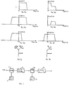
- a typical v.s.b. modulator is shown in simplified form in Figure 1.
- An input baseband signal eg. a video signal is mixed in mixer 1 with an intermediate frequency (i.f.) carrier wave signal produced in an oscillator 2 to produce an amplitude modulated double sideband signal.
- the upper part of the upper sideband is removed in v.s.b. filter 3 and the signal is mixed in mixer 4 with an r.f. signal produced in oscillator 5, the frequency of which differs from the desired r.f. transmission frequency by the i.f. frequency.
- the output of the mixer 4 is filtered by a bandpass channel filter 6 to remove the r.f. carrier and the upper side frequency w c + 2w i.f. .
- both oscillator frequency 5 and the channel filter 6 must be changed.
- the latter presents a problem since the channel filter depends on both the carrier frequency and the i.f. frequency, and is a relatively expensive and specialist item to obtain.
- the invention provides a vestigial sideband modulator comprising first modulating means for modulating a signal derived from an i.f. oscillator with a baseband input signal, vestigial sideband filtering means for filtering the modulated i.f. signal, means for demodulating the filtered modulated i.f. signal to produce baseband components substantially in quadrature using signals derived from the i.f. oscillator, second modulating means for modulating signals which are substantially in quadrature and are derived from a carrier oscillator with the baseband quadrature components, and means for combining the modulated carrier signals to produce a vestigial sideband modulated carrier signal.
- a v.s.b. modulated r.f. output carrier can be produced without the necessity for a channel filter.
- a loop control may be provided to maintain signals in quadrature phase relation derived from the i.f. oscillator and used to produce the baseband components, in-phase and quadrature, with the i.f. carrier wave component of the filtered modulated i.f. signal.
- Advantage may be taken of the fact that the baseband component output that is produced using the quadrature demodulating signal (that is, the signal derived from the i.f. oscillator which is in quadrature phase relation with the i.f. carrier wave component of the filtered modulated i.f. signal) is zero over the part of the frequency spectrum of the v.s.b. filter output that is double side band. Any deviations from zero over this range may be used to shift the phase of the quadrature signals derived from the i.f. oscillator in such a direction as to reduce that baseband component output.
- Audio and digitally modulated signal eg nicam (near instantaneously expanded audio multiplex) signals, modulated onto appropriate subcarriers, may be combined with the demodulated baseband components before modulation onto the carrier signals.
- signals could be combined with the input baseband signal.
- the latter will usually be a vision signal, the invention is applicable to any baseband signal.
- the v.s.b. modulator may be used as a standby transmitter, since it can operate at any frequency to which the carrier oscillator is set, or as video test equipment.
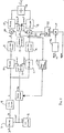
- a composite video signal (the frequency response of which, typically extending to 5.5 MHz, is shown in Figure 3a) forms the input to the modulator, and is fed to a first modulating means in the form of a mixer 7 which amplitude modulates the signal from a local i.f. oscillator 8 (typically 38.9 MHz) to produce double sideband amplitude modulation of the i.f. signal ( Figure 3b).
- the mixer 7 is followed by a vestigial sideband filter 9 which removes the upper part of the upper sideband ( Figure 3c), as in the prior art modulator.
- the v.s.b. filter may be a surface acoustic wave (SAW) filter.
- the mixer 7 in common with the other mixers in the circuit, could instead be implemented as multipliers.
- the modulated i.f. signal is demodulated to baseband quadrature components in mixers 10, 11 by means of quadrature signals fed from a 90° splitter 12 which provides in-phase and quadrature components from the i.f. oscillator 8.
- the frequency bands at around twice the i.f. frequency are removed by low pass filters 13, 14.
- the frequency response of the baseband quadrature components is shown in Figures 3d and 3e.
- the video modulated i.f. carrier may be represented by phasor diagram 3g, in which the carrier, cos w i.f. t is represented by a phasor of length unity and the video signal, A cosw v t, by phasors of length A / 2 which counter-rotate with angular velocity w v .
- the demodulated signal at the output of the mixers 10, 11 is of course represented just by video phasors on their own). It can be appreciated that mixer 10 fed by cos w i.f.
- phase shifter 26 In order to maintain the inputs to the demodulating mixers 10, 11 in phase and quadrature with respect to the i.f. oscillator 0, a phase shifter 26 is provided which varies the phase of the signal from the i.f. oscillator under the control of loop amplifier 27.
- the loop amplifier has a time constant such that it only responds to low frequency signals e.g. below a few hundred Hz. Since the output of the mixer (as explained above) should be zero at these frequencies, any response at these frequencies produces a voltage which causes the phase shifter 26 to vary the phase of the input to the splitter 12 in a direction that reduces that output.
- a tone in the video input may be represented by a cos w v t and the signals produced by the local oscillators may be represented by cos w i.f. t and cos w c t
- the output of the mixer at point b is given by A′ [cos (w i.f. t - w v t) + cos (w i.f. t + w v t)]
- the lower frequency portion of the signal spectrum is double sideband and the upper frequency portion of the signal spectrum is single sideband.
- the respective components are at point c dsb A ⁇ [cos (w i.f. t - w v t) + cos (w i.f. t + w v t)] ssb A ⁇ [cos (w i.f. t - w v t)]
- the components at points d, e are: dsb A′′′ [cos (w v t)) at point d and 0 at point e (the sin (2w i.f. t w v t) components having been filtered out) ssb A′′′ 2 [cos (w v t)) at point d, and A′′′ 2 [sin (w v t)) at point e
- Audio and digital (eg nicam) signals are added to the vision signal by being combined at combiners 20, 21 from a 90° splitter 22 fed via combiner 25 from: an oscillator 24 (eg a VCO or numerically controlled oscillator) driven by an audio input 23 (providing audio frequency modulated onto a carrier operating at the desired difference between sound and vision typically 5.5 MHz): and a nicam input from an encoder (providing nicam stereo modulated onto a typically 6.552MHz carrier).
- the audio and nicam signals could be combined with the vision signal in the baseband input. Such signals need not be combined with a vision signal at drive level, but could be transmitted separately to the vision signals.
- the modulator of the invention possess a number of advantages. Firstly, no channel filter is required since the carrier modulated video output is produced by directly modulating the carrier with video waveform components. It follows that the transmitting frequency can be changed simply by changing the carrier oscillator. Secondly, the long term stability of the i.f. oscillator does not affect the transmitted signal, since the i.f. signal is first modulated by the video signal and then the signal is demodulated to remove the i.f. signal.
- the modulator may be used as a stand-by module for a television transmitter. Such a transmitter, at least in the U.K., will already have four modulators driving respect power amplifiers connected to the transmitting antenna. In the event of a modulator failing, the carrier oscillator 17 can be switched to the appropriate frequency and switched in to replace the defective one.
- a stand-by module could consist of a linear power amplifier and a modulator, which could be switched in to replace a defective module.
- the module could form part of video test equipment in which the device under test requires to be fed with a v.s.b filtered vision r.f. signal at different r.f. carrier frequencies. All that needs to be done is to change the frequency of the carrier oscillator.
- additional processing of the video modulated i.f. signal may be performed before demodulation, i.e. at point c in Figure 2, e.g. precorrection to compensate for distortion in a klystron power amplifier.
- the invention is not restricted to baseband video signals, but is applicable to other types of baseband input signal.
Landscapes
- Engineering & Computer Science (AREA)
- Multimedia (AREA)
- Signal Processing (AREA)
- Amplitude Modulation (AREA)
- Digital Transmission Methods That Use Modulated Carrier Waves (AREA)
Abstract
Description
- This invention relates to vestigial sideband (v.s.b.) modulators.
- Vestigial sideband modulators are used in television transmitters for modulating a video signal onto an r.f. carrier so that the modulated carrier has a vestigial sideband.
- A typical v.s.b. modulator is shown in simplified form in Figure 1. An input baseband signal eg. a video signal is mixed in mixer 1 with an intermediate frequency (i.f.) carrier wave signal produced in an
oscillator 2 to produce an amplitude modulated double sideband signal. The upper part of the upper sideband is removed in v.s.b. filter 3 and the signal is mixed inmixer 4 with an r.f. signal produced in oscillator 5, the frequency of which differs from the desired r.f. transmission frequency by the i.f. frequency. The output of themixer 4 is filtered by a bandpass channel filter 6 to remove the r.f. carrier and the upper side frequency wc + 2wi.f.. - If it is desired to transmit at a different frequency, both oscillator frequency 5 and the channel filter 6 must be changed. The latter presents a problem since the channel filter depends on both the carrier frequency and the i.f. frequency, and is a relatively expensive and specialist item to obtain.
- The invention provides a vestigial sideband modulator comprising first modulating means for modulating a signal derived from an i.f. oscillator with a baseband input signal, vestigial sideband filtering means for filtering the modulated i.f. signal, means for demodulating the filtered modulated i.f. signal to produce baseband components substantially in quadrature using signals derived from the i.f. oscillator, second modulating means for modulating signals which are substantially in quadrature and are derived from a carrier oscillator with the baseband quadrature components, and means for combining the modulated carrier signals to produce a vestigial sideband modulated carrier signal.
- By demodulating the modulated i.f. signals to baseband after v.s.b. filtering and using the resulting quadrature components to modulate the quadrature signals at the output carrier frequency, a v.s.b. modulated r.f. output carrier can be produced without the necessity for a channel filter.
- A loop control may be provided to maintain signals in quadrature phase relation derived from the i.f. oscillator and used to produce the baseband components, in-phase and quadrature, with the i.f. carrier wave component of the filtered modulated i.f. signal. Advantage may be taken of the fact that the baseband component output that is produced using the quadrature demodulating signal (that is, the signal derived from the i.f. oscillator which is in quadrature phase relation with the i.f. carrier wave component of the filtered modulated i.f. signal) is zero over the part of the frequency spectrum of the v.s.b. filter output that is double side band. Any deviations from zero over this range may be used to shift the phase of the quadrature signals derived from the i.f. oscillator in such a direction as to reduce that baseband component output.
- Audio and digitally modulated signal eg nicam (near instantaneously expanded audio multiplex) signals, modulated onto appropriate subcarriers, may be combined with the demodulated baseband components before modulation onto the carrier signals. Alternatively, such signals could be combined with the input baseband signal. Although the latter will usually be a vision signal, the invention is applicable to any baseband signal.
- The v.s.b. modulator may be used as a standby transmitter, since it can operate at any frequency to which the carrier oscillator is set, or as video test equipment.
- A vestigial sideband modulator of a television transmitter constructed in accordance with the invention will now be described, by way of example, with reference to Figures 2 and 3 of the accompanying drawings, in which:
- Figure 2 is a block diagram of the v.s.b. modulator; and
- Figure 3 shows the frequency response at various points in the modulator.
- A composite video signal (the frequency response of which, typically extending to 5.5 MHz, is shown in Figure 3a) forms the input to the modulator, and is fed to a first modulating means in the form of a mixer 7 which amplitude modulates the signal from a local i.f. oscillator 8 (typically 38.9 MHz) to produce double sideband amplitude modulation of the i.f. signal (Figure 3b). The mixer 7 is followed by a
vestigial sideband filter 9 which removes the upper part of the upper sideband (Figure 3c), as in the prior art modulator. The v.s.b. filter may be a surface acoustic wave (SAW) filter. The mixer 7 in common with the other mixers in the circuit, could instead be implemented as multipliers. - Instead of changing the modulated i.f. signal to carrier frequency directly as in the prior art, the modulated i.f. signal is demodulated to baseband quadrature components in
mixers 10, 11 by means of quadrature signals fed from a 90°splitter 12 which provides in-phase and quadrature components from the i.f.oscillator 8. The frequency bands at around twice the i.f. frequency are removed bylow pass filters - The frequency response of the baseband quadrature components is shown in Figures 3d and 3e. At low frequencies for which both sidebands are passed by the v.s.b.
filter 9, the video modulated i.f. carrier may be represented by phasor diagram 3g, in which the carrier, cos wi.f.t is represented by a phasor of length unity and the video signal, A coswvt, by phasors of length A/2 which counter-rotate with angular velocity wv. (The demodulated signal at the output of themixers 10, 11 is of course represented just by video phasors on their own). It can be appreciated thatmixer 10 fed by cos wi.f.t will (after filtering of the sum components in low pass filter 13) produce an output response at low video frequencies (since the video phasor has a resultant component parallel to the carrier phasor) but that the mixer 11 fed by sin wi.f.t (again, after filtering of the sum components in low pass filter 13) will not, since the video phasor never has any resultant component at right angles to the carrier phasor. The phasors representing the video signal always cancel in the sin wi.f.t direction which is at right angles to the carrier phasor. - At higher video frequencies, when the operation is single sideband (s.s.b.) rather than double sideband (d.s.b.), the video modulated i.f. carrier has only one sideband hence is represented by Figure 3h. It follows that the output of the
mixer 10 is halved (Figure 3d) at these frequencies, since the component of the video phasor in the direction of the carrier is halved, and there is a component of the same size in the sin wi.f.t direction (Figure 3e). - In order to maintain the inputs to the
demodulating mixers 10, 11 in phase and quadrature with respect to the i.f. oscillator 0, aphase shifter 26 is provided which varies the phase of the signal from the i.f. oscillator under the control ofloop amplifier 27. The loop amplifier has a time constant such that it only responds to low frequency signals e.g. below a few hundred Hz. Since the output of the mixer (as explained above) should be zero at these frequencies, any response at these frequencies produces a voltage which causes thephase shifter 26 to vary the phase of the input to thesplitter 12 in a direction that reduces that output. - When the demodulated baseband components are mixed at
mixers local oscillator 17 at carrier frequency via 90°splitter 18, and combined atcombiner 19, a v.s.b. modulated video output at carrier frequency wc is obtained (Figure 3f). - Thus, if a tone in the video input may be represented by a cos wvt and the signals produced by the local oscillators may be represented by cos wi.f.t and cos wct, the output of the mixer at point b is given by

- After filtering, the lower frequency portion of the signal spectrum is double sideband and the upper frequency portion of the signal spectrum is single sideband. The respective components are at point c


- After demodulation to baseband quadrature components and low pass filtering, the components at points d, e are: dsb A‴ [cos (wvt)) at point d and 0 at point e (the sin (2wi.f.t wvt) components having been filtered out) ssb


- When these are modulated onto quadrature carrier components, one obtains at point f


- It will be noted that this corresponds to the desired signal since it is the same as appears at point c except that the signal is now at carrier frequency instead of i.f. frequency. There is a phase change of 90° which does not make any difference i.e. the expression uses sines not cosines, and there is a change of sign in the single sideband expression which represents the fact that the vestigial sideband is now lower rather than higher than the carrier frequency. In fact it would be possible for the v.s.b. filter 9 to attenuate the lower rather than the upper sideband, in which the case the same required output at point f could be produced by reversing the sine and cosine inputs at
mixers - It should be noted that acceptable results may be obtained if the
splitters splitters - Audio and digital (eg nicam) signals are added to the vision signal by being combined at
combiners splitter 22 fed viacombiner 25 from: an oscillator 24 (eg a VCO or numerically controlled oscillator) driven by an audio input 23 (providing audio frequency modulated onto a carrier operating at the desired difference between sound and vision typically 5.5 MHz): and a nicam input from an encoder (providing nicam stereo modulated onto a typically 6.552MHz carrier). Alternatively, the audio and nicam signals could be combined with the vision signal in the baseband input. Such signals need not be combined with a vision signal at drive level, but could be transmitted separately to the vision signals. - The modulator of the invention possess a number of advantages. Firstly, no channel filter is required since the carrier modulated video output is produced by directly modulating the carrier with video waveform components. It follows that the transmitting frequency can be changed simply by changing the carrier oscillator. Secondly, the long term stability of the i.f. oscillator does not affect the transmitted signal, since the i.f. signal is first modulated by the video signal and then the signal is demodulated to remove the i.f. signal.
- The modulator may be used as a stand-by module for a television transmitter. Such a transmitter, at least in the U.K., will already have four modulators driving respect power amplifiers connected to the transmitting antenna. In the event of a modulator failing, the
carrier oscillator 17 can be switched to the appropriate frequency and switched in to replace the defective one. Alternatively, a stand-by module could consist of a linear power amplifier and a modulator, which could be switched in to replace a defective module. - Alternatively, the module could form part of video test equipment in which the device under test requires to be fed with a v.s.b filtered vision r.f. signal at different r.f. carrier frequencies. All that needs to be done is to change the frequency of the carrier oscillator.
- If desired, additional processing of the video modulated i.f. signal may be performed before demodulation, i.e. at point c in Figure 2, e.g. precorrection to compensate for distortion in a klystron power amplifier.
- The invention is not restricted to baseband video signals, but is applicable to other types of baseband input signal.
Claims (4)
- A v.s.b modulator comprising first modulating means for modulating a signal derived from an i.f. oscillator with a baseband input signal, vestigial sideband filtering means for filtering the modulated i.f. signal, means for demodulating the filtered modulated i.f. signal to produce baseband components substantially in quadrature using signals derived from the i.f. oscillator, second modulating means for modulating signals which are substantially in quadrature and are derived from a carrier oscillator with the baseband quadrature components, and means for combining the modulated carrier signals to produce a vestigial sideband modulated carrier signal.
- A v.s.b. modulator as claimed in claim 1, in which the demodulating means includes means for splitting the i.f. signal into substantially in-phase and quadrature components, and phase shifting means to adjust the phase of the i.f. signal fed to the splitting means to maintain one of the components in quadrature with respect to the phase of the i.f. component of the modulated i.f. signal.
- A v.s.b. modulator as claimed in claim 2, in which the phase shifting means is arranged to adjust the phase so as to maintain zero output of low frequencies in the baseband component that is in quadrature with the i.f. component of the modulated i.f. signal.
- A v.s.b. modulator as claimed in claim 1, including means for combining substantially quadrature components of a subcarrier frequency modulated by a subsidiary input.
Applications Claiming Priority (2)
| Application Number | Priority Date | Filing Date | Title |
|---|---|---|---|
| GB9107652 | 1991-04-11 | ||
| GB9107652A GB2254744B (en) | 1991-04-11 | 1991-04-11 | Vestigial sideband modulator |
Publications (2)
| Publication Number | Publication Date |
|---|---|
| EP0508741A2 true EP0508741A2 (en) | 1992-10-14 |
| EP0508741A3 EP0508741A3 (en) | 1993-09-15 |
Family
ID=10693046
Family Applications (1)
| Application Number | Title | Priority Date | Filing Date |
|---|---|---|---|
| EP19920303101 Ceased EP0508741A3 (en) | 1991-04-11 | 1992-04-08 | Vestigial sideband modulator |
Country Status (4)
| Country | Link |
|---|---|
| US (1) | US5243304A (en) |
| EP (1) | EP0508741A3 (en) |
| GB (1) | GB2254744B (en) |
| NO (1) | NO921399L (en) |
Cited By (5)
| Publication number | Priority date | Publication date | Assignee | Title |
|---|---|---|---|---|
| US5822020A (en) * | 1995-03-10 | 1998-10-13 | M.B. International S.R.L. | Method and device for generating a modulated television signal |
| WO1999004558A1 (en) * | 1997-07-18 | 1999-01-28 | Rohde & Schwarz Gmbh & Co. Kg | Method and device for vestigial sideband modulation of a television transmitter |
| WO2000045503A1 (en) * | 1999-01-29 | 2000-08-03 | Adc Broadband Wireless Group Inc. | Vestigial sideband generator particularly for digital television |
| WO2001078392A2 (en) * | 2000-04-07 | 2001-10-18 | Adc Broadband Wireless Group, Inc. | Reduced bandwidth transmitter method and apparatus |
| WO2001080419A2 (en) * | 2000-04-18 | 2001-10-25 | Microtune (Texas), L.P. | System and method for frequency translation using an image reject mixer |
Families Citing this family (6)
| Publication number | Priority date | Publication date | Assignee | Title |
|---|---|---|---|---|
| US5373265A (en) * | 1993-07-06 | 1994-12-13 | At&T Corp. | Modulator having oscillator for generating IF and RF signals by division and up-conversion |
| IT1276019B1 (en) * | 1995-03-10 | 1997-10-24 | M B International S R L | PROCEDURE FOR THE GENERATION OF A MODULATED TELEVISION SIGNAL |
| JPH10224150A (en) * | 1997-02-05 | 1998-08-21 | Matsushita Electric Ind Co Ltd | Video signal transmission device |
| US5861781A (en) * | 1997-09-16 | 1999-01-19 | Lucent Technologies Inc. | Single sideband double quadrature modulator |
| US6184921B1 (en) * | 1998-02-20 | 2001-02-06 | Samsung Electronics Co., Ltd. | Method for transmitting VSB digital TV with carrier frequency near co-channel NTSC audio carrier frequency |
| US6667760B1 (en) * | 1998-02-20 | 2003-12-23 | Samsung Electronics Co., Ltd. | Receiver for digital television signals having carriers near upper frequency boundaries of TV broadcasting channels |
Citations (3)
| Publication number | Priority date | Publication date | Assignee | Title |
|---|---|---|---|---|
| US3835391A (en) * | 1971-05-21 | 1974-09-10 | Ibm | Vestigial sideband signal generator |
| US3955155A (en) * | 1974-12-23 | 1976-05-04 | Rca Corporation | Amplitude modulation system |
| JPS59198052A (en) * | 1983-04-26 | 1984-11-09 | Fujitsu Ltd | Phase locked circuit |
Family Cites Families (3)
| Publication number | Priority date | Publication date | Assignee | Title |
|---|---|---|---|---|
| GB913089A (en) * | 1960-10-26 | 1962-12-19 | Communications Patents Ltd | Improvements in or relating to multi-channel electric wave signalling systems |
| NL301914A (en) * | 1962-12-18 | |||
| JPH088452B2 (en) * | 1989-06-08 | 1996-01-29 | 株式会社ケンウッド | SSB modulator and SSB demodulator |
-
1991
- 1991-04-11 GB GB9107652A patent/GB2254744B/en not_active Expired - Fee Related
-
1992
- 1992-04-07 US US07/864,877 patent/US5243304A/en not_active Expired - Fee Related
- 1992-04-08 EP EP19920303101 patent/EP0508741A3/en not_active Ceased
- 1992-04-09 NO NO92921399A patent/NO921399L/en unknown
Patent Citations (3)
| Publication number | Priority date | Publication date | Assignee | Title |
|---|---|---|---|---|
| US3835391A (en) * | 1971-05-21 | 1974-09-10 | Ibm | Vestigial sideband signal generator |
| US3955155A (en) * | 1974-12-23 | 1976-05-04 | Rca Corporation | Amplitude modulation system |
| JPS59198052A (en) * | 1983-04-26 | 1984-11-09 | Fujitsu Ltd | Phase locked circuit |
Non-Patent Citations (1)
| Title |
|---|
| PATENT ABSTRACTS OF JAPAN vol. 9, no. 56 (E-302)12 March 1985 & JP-A-59 198 052 ( FUJITSU ) * |
Cited By (12)
| Publication number | Priority date | Publication date | Assignee | Title |
|---|---|---|---|---|
| US5822020A (en) * | 1995-03-10 | 1998-10-13 | M.B. International S.R.L. | Method and device for generating a modulated television signal |
| WO1999004558A1 (en) * | 1997-07-18 | 1999-01-28 | Rohde & Schwarz Gmbh & Co. Kg | Method and device for vestigial sideband modulation of a television transmitter |
| DE19731012B4 (en) * | 1997-07-18 | 2006-08-03 | Rohde & Schwarz Gmbh & Co. Kg | Arrangement for generating a vestigial sideband modulated video signal with residual carrier for a television station |
| WO2000045503A1 (en) * | 1999-01-29 | 2000-08-03 | Adc Broadband Wireless Group Inc. | Vestigial sideband generator particularly for digital television |
| US6724832B1 (en) | 1999-01-29 | 2004-04-20 | Adc Broadband Wireless Group, Inc. | Vestigial sideband generator particularly for digital television |
| WO2001078392A2 (en) * | 2000-04-07 | 2001-10-18 | Adc Broadband Wireless Group, Inc. | Reduced bandwidth transmitter method and apparatus |
| WO2001078392A3 (en) * | 2000-04-07 | 2003-04-03 | Adc Broadband Wireless Group I | Reduced bandwidth transmitter method and apparatus |
| WO2001080419A2 (en) * | 2000-04-18 | 2001-10-25 | Microtune (Texas), L.P. | System and method for frequency translation using an image reject mixer |
| WO2001080419A3 (en) * | 2000-04-18 | 2002-05-23 | Microtune Texas Lp | System and method for frequency translation using an image reject mixer |
| US7184724B1 (en) | 2000-04-18 | 2007-02-27 | Microtune (Texas), L.P. | System and method for frequency translation using an image reject mixer |
| US7403761B2 (en) | 2000-04-18 | 2008-07-22 | Microtune (Texas), L.P. | System and method for frequency translation using an image reject mixer |
| US7711346B2 (en) | 2000-04-18 | 2010-05-04 | Microtune (Texas), L.P. | System and method for frequency translation using an image reject mixer |
Also Published As
| Publication number | Publication date |
|---|---|
| NO921399D0 (en) | 1992-04-09 |
| GB9107652D0 (en) | 1991-05-29 |
| US5243304A (en) | 1993-09-07 |
| GB2254744A (en) | 1992-10-14 |
| NO921399L (en) | 1992-10-12 |
| EP0508741A3 (en) | 1993-09-15 |
| GB2254744B (en) | 1994-12-21 |
Similar Documents
| Publication | Publication Date | Title |
|---|---|---|
| US5243304A (en) | Vestigial sideband modulator for a baseband input signal | |
| US6560297B1 (en) | Image rejection downconverter for a translation loop modulator | |
| US4908860A (en) | System for the secret transmission of audio signals and television receiver for receiving such signals | |
| US4955072A (en) | Method of generating an amplitude-modulated ISB transmission signal and apparatus for carrying out the method | |
| CA1229407A (en) | Transmission system for tv signals on radio links | |
| US3349184A (en) | Bandwidth compression and expansion by frequency division and multiplication | |
| JPS58166840A (en) | Fm receiver | |
| US4100376A (en) | Pilot tone demodulator | |
| CA1259400A (en) | Modulation device | |
| US2630497A (en) | Frequency modulation multiplex system | |
| US4973923A (en) | Circuit arrangement for the generation of I,Q waveforms | |
| US4220818A (en) | AM Stereo transmitter | |
| JPS6237580B2 (en) | ||
| US4097813A (en) | Carrier wave recovery circuit | |
| GB2300318A (en) | Improvements in or relating to transceivers | |
| US4075565A (en) | Single side-band wave generation system | |
| US4910798A (en) | Reverse Nyquist slope filter | |
| JPH0282703A (en) | Frequency convertor | |
| US3375444A (en) | Vestigial sideband modulator circuit | |
| US5061999A (en) | Multiplex signal processing apparatus | |
| JPH05268188A (en) | Multiplex radio modulator-demodulator | |
| SU1693726A1 (en) | Method of transmission and reception of analog signals and device to implement it | |
| JPH04239804A (en) | Demodulation circuit | |
| GB778406A (en) | Improvements in or relating to multiplex television transmission systems and transmitters and receivers for use in such systems | |
| KR810000344B1 (en) | Transmitter |
Legal Events
| Date | Code | Title | Description |
|---|---|---|---|
| PUAI | Public reference made under article 153(3) epc to a published international application that has entered the european phase |
Free format text: ORIGINAL CODE: 0009012 |
|
| AK | Designated contracting states |
Kind code of ref document: A2 Designated state(s): BE DE ES FR NL SE |
|
| PUAL | Search report despatched |
Free format text: ORIGINAL CODE: 0009013 |
|
| AK | Designated contracting states |
Kind code of ref document: A3 Designated state(s): BE DE ES FR NL SE |
|
| 17P | Request for examination filed |
Effective date: 19940310 |
|
| GRAG | Despatch of communication of intention to grant |
Free format text: ORIGINAL CODE: EPIDOS AGRA |
|
| 17Q | First examination report despatched |
Effective date: 19961114 |
|
| STAA | Information on the status of an ep patent application or granted ep patent |
Free format text: STATUS: THE APPLICATION HAS BEEN REFUSED |
|
| 18R | Application refused |
Effective date: 19970503 |