EP0500818B1 - Method for controlling a power converter using an auxiliary resonant commutation circuit - Google Patents
Method for controlling a power converter using an auxiliary resonant commutation circuit Download PDFInfo
- Publication number
- EP0500818B1 EP0500818B1 EP91909925A EP91909925A EP0500818B1 EP 0500818 B1 EP0500818 B1 EP 0500818B1 EP 91909925 A EP91909925 A EP 91909925A EP 91909925 A EP91909925 A EP 91909925A EP 0500818 B1 EP0500818 B1 EP 0500818B1
- Authority
- EP
- European Patent Office
- Prior art keywords
- current
- switching devices
- main switching
- resonant
- coupled
- Prior art date
- Legal status (The legal status is an assumption and is not a legal conclusion. Google has not performed a legal analysis and makes no representation as to the accuracy of the status listed.)
- Expired - Lifetime
Links
Images


Classifications
-
- H—ELECTRICITY
- H02—GENERATION; CONVERSION OR DISTRIBUTION OF ELECTRIC POWER
- H02M—APPARATUS FOR CONVERSION BETWEEN AC AND AC, BETWEEN AC AND DC, OR BETWEEN DC AND DC, AND FOR USE WITH MAINS OR SIMILAR POWER SUPPLY SYSTEMS; CONVERSION OF DC OR AC INPUT POWER INTO SURGE OUTPUT POWER; CONTROL OR REGULATION THEREOF
- H02M7/00—Conversion of ac power input into dc power output; Conversion of dc power input into ac power output
- H02M7/42—Conversion of dc power input into ac power output without possibility of reversal
- H02M7/44—Conversion of dc power input into ac power output without possibility of reversal by static converters
- H02M7/48—Conversion of dc power input into ac power output without possibility of reversal by static converters using discharge tubes with control electrode or semiconductor devices with control electrode
- H02M7/4826—Conversion of dc power input into ac power output without possibility of reversal by static converters using discharge tubes with control electrode or semiconductor devices with control electrode operating from a resonant DC source, i.e. the DC input voltage varies periodically, e.g. resonant DC-link inverters
-
- H—ELECTRICITY
- H02—GENERATION; CONVERSION OR DISTRIBUTION OF ELECTRIC POWER
- H02M—APPARATUS FOR CONVERSION BETWEEN AC AND AC, BETWEEN AC AND DC, OR BETWEEN DC AND DC, AND FOR USE WITH MAINS OR SIMILAR POWER SUPPLY SYSTEMS; CONVERSION OF DC OR AC INPUT POWER INTO SURGE OUTPUT POWER; CONTROL OR REGULATION THEREOF
- H02M7/00—Conversion of ac power input into dc power output; Conversion of dc power input into ac power output
- H02M7/42—Conversion of dc power input into ac power output without possibility of reversal
- H02M7/44—Conversion of dc power input into ac power output without possibility of reversal by static converters
- H02M7/48—Conversion of dc power input into ac power output without possibility of reversal by static converters using discharge tubes with control electrode or semiconductor devices with control electrode
- H02M7/505—Conversion of dc power input into ac power output without possibility of reversal by static converters using discharge tubes with control electrode or semiconductor devices with control electrode using devices of a thyratron or thyristor type requiring extinguishing means
- H02M7/515—Conversion of dc power input into ac power output without possibility of reversal by static converters using discharge tubes with control electrode or semiconductor devices with control electrode using devices of a thyratron or thyristor type requiring extinguishing means using semiconductor devices only
- H02M7/523—Conversion of dc power input into ac power output without possibility of reversal by static converters using discharge tubes with control electrode or semiconductor devices with control electrode using devices of a thyratron or thyristor type requiring extinguishing means using semiconductor devices only with LC-resonance circuit in the main circuit
-
- H—ELECTRICITY
- H02—GENERATION; CONVERSION OR DISTRIBUTION OF ELECTRIC POWER
- H02M—APPARATUS FOR CONVERSION BETWEEN AC AND AC, BETWEEN AC AND DC, OR BETWEEN DC AND DC, AND FOR USE WITH MAINS OR SIMILAR POWER SUPPLY SYSTEMS; CONVERSION OF DC OR AC INPUT POWER INTO SURGE OUTPUT POWER; CONTROL OR REGULATION THEREOF
- H02M7/00—Conversion of ac power input into dc power output; Conversion of dc power input into ac power output
- H02M7/42—Conversion of dc power input into ac power output without possibility of reversal
- H02M7/44—Conversion of dc power input into ac power output without possibility of reversal by static converters
- H02M7/48—Conversion of dc power input into ac power output without possibility of reversal by static converters using discharge tubes with control electrode or semiconductor devices with control electrode
- H02M7/505—Conversion of dc power input into ac power output without possibility of reversal by static converters using discharge tubes with control electrode or semiconductor devices with control electrode using devices of a thyratron or thyristor type requiring extinguishing means
- H02M7/515—Conversion of dc power input into ac power output without possibility of reversal by static converters using discharge tubes with control electrode or semiconductor devices with control electrode using devices of a thyratron or thyristor type requiring extinguishing means using semiconductor devices only
- H02M7/5152—Conversion of dc power input into ac power output without possibility of reversal by static converters using discharge tubes with control electrode or semiconductor devices with control electrode using devices of a thyratron or thyristor type requiring extinguishing means using semiconductor devices only with separate extinguishing means
-
- H—ELECTRICITY
- H02—GENERATION; CONVERSION OR DISTRIBUTION OF ELECTRIC POWER
- H02M—APPARATUS FOR CONVERSION BETWEEN AC AND AC, BETWEEN AC AND DC, OR BETWEEN DC AND DC, AND FOR USE WITH MAINS OR SIMILAR POWER SUPPLY SYSTEMS; CONVERSION OF DC OR AC INPUT POWER INTO SURGE OUTPUT POWER; CONTROL OR REGULATION THEREOF
- H02M7/00—Conversion of ac power input into dc power output; Conversion of dc power input into ac power output
- H02M7/42—Conversion of dc power input into ac power output without possibility of reversal
- H02M7/44—Conversion of dc power input into ac power output without possibility of reversal by static converters
- H02M7/48—Conversion of dc power input into ac power output without possibility of reversal by static converters using discharge tubes with control electrode or semiconductor devices with control electrode
- H02M7/505—Conversion of dc power input into ac power output without possibility of reversal by static converters using discharge tubes with control electrode or semiconductor devices with control electrode using devices of a thyratron or thyristor type requiring extinguishing means
- H02M7/515—Conversion of dc power input into ac power output without possibility of reversal by static converters using discharge tubes with control electrode or semiconductor devices with control electrode using devices of a thyratron or thyristor type requiring extinguishing means using semiconductor devices only
- H02M7/523—Conversion of dc power input into ac power output without possibility of reversal by static converters using discharge tubes with control electrode or semiconductor devices with control electrode using devices of a thyratron or thyristor type requiring extinguishing means using semiconductor devices only with LC-resonance circuit in the main circuit
- H02M7/5233—Conversion of dc power input into ac power output without possibility of reversal by static converters using discharge tubes with control electrode or semiconductor devices with control electrode using devices of a thyratron or thyristor type requiring extinguishing means using semiconductor devices only with LC-resonance circuit in the main circuit the commutation elements being in a push-pull arrangement
- H02M7/5236—Conversion of dc power input into ac power output without possibility of reversal by static converters using discharge tubes with control electrode or semiconductor devices with control electrode using devices of a thyratron or thyristor type requiring extinguishing means using semiconductor devices only with LC-resonance circuit in the main circuit the commutation elements being in a push-pull arrangement in a series push-pull arrangement
-
- H—ELECTRICITY
- H02—GENERATION; CONVERSION OR DISTRIBUTION OF ELECTRIC POWER
- H02M—APPARATUS FOR CONVERSION BETWEEN AC AND AC, BETWEEN AC AND DC, OR BETWEEN DC AND DC, AND FOR USE WITH MAINS OR SIMILAR POWER SUPPLY SYSTEMS; CONVERSION OF DC OR AC INPUT POWER INTO SURGE OUTPUT POWER; CONTROL OR REGULATION THEREOF
- H02M7/00—Conversion of ac power input into dc power output; Conversion of dc power input into ac power output
- H02M7/42—Conversion of dc power input into ac power output without possibility of reversal
- H02M7/44—Conversion of dc power input into ac power output without possibility of reversal by static converters
- H02M7/48—Conversion of dc power input into ac power output without possibility of reversal by static converters using discharge tubes with control electrode or semiconductor devices with control electrode
- H02M7/4811—Conversion of dc power input into ac power output without possibility of reversal by static converters using discharge tubes with control electrode or semiconductor devices with control electrode having auxiliary actively switched resonant commutation circuits connected to intermediate DC voltage or between two push-pull branches
Definitions
- the present invention relates generally to power converters. More particularly, the present invention relates to a method for controlling a resonant power converter by suitably controlling an auxiliary resonant commutation circuit to achieve soft-switching of the converter's switching devices.
- soft-switching converters To overcome the problem of active device switching losses in power converters, while enabling operation at higher switching frequencies, soft-switching converters have been developed. In general, there are two types of soft-switching, or resonant, converters: zero-voltage switching and zero-current switching. Zero-voltage switching involves switching the active devices when there is zero voltage thereacross. Zero-current switching involves switching the active devices when there is zero current therethrough. Unfortunately, however, higher voltage or current stresses generally result from operation of such soft-switching power converters, necessitating the use of devices with higher voltage or current ratings, respectively.
- the control initially provides a turn-off signal to one of the main switching devices of an inverter pole, and subsequently triggers an auxiliary switching device to provide a temporary path to take over the high-stress, turn-on duty from the other main switching device of the inverter pole in a manner that leaves no energy trapped after switching.
- the LC resonant circuit ideally swings the output voltage from one power rail to the other, at which time the opposite main switching device is turned on.
- this resonant snubber circuit topology does not impose any voltage or current penalties on the main devices.
- each inverter phase can be controlled independently using pulse width modulation, resulting in converter waveforms having low harmonic distortion.
- the resonant output voltage may fall short of the opposite rail voltage due to component resistances, device conduction losses and inadequate forcing potential.
- the next switching device in the inverter pole to be turned on may be switched at the peak of the resonating voltage, and hence must absorb some switching losses due to the non-zero voltage turn-on, including the energy dump from the parallel capacitor.
- the resonant snubber circuit topology exhibits reduced main device stresses during switching instants and substantially reduced switching losses, it is desirable to reduce switching losses and associated EMI noise even further and thus more closely approach truly "lossless" switching.
- the present invention seeks to provide a new and improved method for controlling a power converter by using and suitably controlling an auxiliary resonant commutation circuit in order to achieve soft-switching of all switching devices employed in the power converter.
- the present invention seeks to provide a method for controlling a power converter employing an auxiliary resonant commutation circuit in order to achieve soft-switching of all of the converter's switching devices such that high quality ac line current waveforms are attainable even with a reduced filter size and at high switching frequencies.
- this embodiment seeks to provide a method for controlling a power converter employing an auxiliary resonant commutation circuit whereby the gating and conduction times of the converter's switching devices are controlled in such manner as to generate a boost energy which is added to the resonant operation in order to ensure soft-switching of all the switching devices.
- a method for controlling a power converter of the type including an inverter having at least one phase, said inverter having at least two series-coupled main switching devices per phase, said series-coupled main switching devices being coupled to positive and negative rails of a dc supply, the junction between said main switching devices being coupled to a load, said main switching devices each having a snubber capacitor coupled in parallel therewith and an antiparallel diode coupled thereacross, said power converter further including a pair of series-coupled bus-splitting capacitors coupled between said positive and negative rails of said dc supply, said power converter further including an auxiliary resonant commutation circuit coupled between the junction joining said main switching devices and the junction joining said bus-splitting capacitors, said auxiliary resonant commutation circuit comprising a pair of antiparallel-coupled auxiliary switching devices coupled in series with a resonant circuit, said resonant circuit including an inductor and said sn
- the auxiliary resonant commutation circuit is triggered into conduction by a respective auxiliary switching device, thereby coupling the LC resonant circuit to a forcing potential substantially equal to one-half the dc supply voltage.
- the output resonating voltage should ideally have a peak-to-peak excursion equal to the dc supply voltage.
- the control method of the present invention involves adding a boost current to the resonant current by appropriately controlling the conduction times of the auxiliary switching devices and the main switching devices.
- a predetermined boost current level adds sufficient energy to the resonant operation to ensure that the output voltage attempts to overshoot the respective converter rail voltages, hence forward biasing the corresponding antiparallel diode and clamping the output voltage to the respective rail voltage.
- the control commutates the corresponding switching device with substantially no switching losses.
- Figure 1 illustrates an inverter pole 10 and an associated auxiliary resonant commutation circuit 12 which may be advantageously controlled according to the method of the present invention in order to achieve soft-switching of all active devices therein, resulting in a highly efficient power converter.
- operation of only one inverter pole, or phase leg, is described and illustrated herein, it is to be understood that the control method of the present invention is applicable to power converters having any number of inverter phases.
- Multiphase full-bridge inverter configurations are well known in the art.
- An exemplary multiphase full-bridge inverter is described in Divan U.S. Pat. No. 4,730,242, issued March 8, 1988, which patent is incorporated by reference herein.
- the control method of the present invention is described with reference to a voltage-source inverter, the principles thereof are equally applicable to current-source inverters.
- inverter pole 10 is shown as comprising two main switching devices S1 and S2 coupled in series across the positive and negative rails p and n, respectively, of the dc supply V dc .
- Each switching device S1 and S2 has a diode D1 and D2, respectively, connected in antiparallel therewith, and further has a relatively large snubber capacitor C r 2 connected thereacross.
- a load inductor LF is shown coupled to the junction between the snubber capacitors.
- switching devices S1 and S2 are illustrated as gate turn-off thyristors (GTO's), the control method of the present invention is applicable to power converters using other suitable self-turn-off switching devices, such as MOSFET's, bipolar junction transistors (BJT's), MOS-controlled thyristors (MCT's), or insulated gate bipolar transistors (IGBT's).
- Auxiliary resonant commutation circuit 12 is coupled between the juncture of switching devices S1 and S2 and the juncture of a pair of substantially equivalent "bus-splitting" filter capacitors 2C dc , which capacitors are connected in series across the dc supply V dc .
- Capacitors 2C dc may comprise, for example, a center-tapped dc filter capacitor.
- Auxiliary resonant commutation circuit 12 inciudes two auxiliary switching devices A1 and A2 having their anodes coupled together. Each auxiliary switching device A1 and A2 has a diode D3 and D4, respectively, connected in antiparallel therewith.
- Auxiliary resonant commutation circuit 12 further includes a resonant inductor L r which is coupled in series with the total effective snubber capacitance C r (i.e. capacitors C r 2 coupled in parallel) during the resonant commutation cycle, as described hereinbelow.
- auxiliary switching devices A1 and A2 are also shown in Figure 1 as comprising GTO's, but other suitable auxiliary switching devices may comprise silicon controlled rectifiers (SCR's), zero-current turn-off thyristors (ZTO's), gate assisted turn-off thyristors (GATO's), or MOS-controlled thyristors (MCT's).
- SCR's silicon controlled rectifiers
- ZTO's zero-current turn-off thyristors
- GTO's gate assisted turn-off thyristors
- MCT's MOS-controlled thyristors
- a control method for determining the gating sequence and conduction times of main switching devices S1 and S2 and auxiliary switching devices A1 and A2 to achieve soft-switching thereof.
- the timing is controlled in such a manner as to provide a boost current ib (shown in Figure 3) which, when added to the resonant inductor current i r (shown in Figure 3), ensures that the resonant output voltage V F attempts to overshoot the dc rail voltages p and n during each resonant interval.
- the corresponding diode D1 or D2 is forward biased, clamping the resonant voltage V F to the respective rail p or n.
- This diode clamping interval provides a zero-voltage turn-on opportunity for the main switching devices S1 and S2. Furthermore, since the main switching devices turn off with a relatively large capacitance in parallel, there are substantially no main device turn-off switching losses, i.e. turn-off occurs with substantially zero voltage thereacross. Still further, the auxiliary switching devices exhibit substantially lossless switching. In particular, the auxiliary switching devices turn on with substantially zero current therethrough due to the presence of a relatively large inductor coupled in series therewith; and the auxiliary switching devices turn off when the resonant current reaches zero, i.e. with substantially zero current therethrough. Hence, soft-switching of all active devices employed in the power converter is achieved by the control method of the present invention.
- Figures 2a-2g schematically illustrate the sequence and directions of current flow in the circuit of Figure 1 when commutation is initiated with current flowing in antiparallel diode D2 in accordance with the control method of the present invention.
- the arrows indicate the directions of current flow, and the conducting devices are indicated by stippling.
- Figure 3 graphically illustrates the resonant and load currents i r and I L , respectively, and the resonant output voltage V F .
- the time intervals during which the respective circuit devices are active are indicated by dashed vertical lines.
- the positive direction of the load current I L is defined in Figure 1, and it will be assumed to be a constant current source during any commutation interval.
- the commutation process begins by turning on auxiliary switching device A2 ( Figure 2b).
- a forcing potential equal to one-half the dc supply V dc 2 is applied across resonant inductor L r .
- This initiates a ramp-up commutation phase wherein the resonant current i r increases at a linear rate of V dc 2L r , as shown in Figure 3.
- main switching device S2 remains gated on, even though it is not conducting current.
- the resonant current i r increases, it displaces the load current initially flowing in diode D2.
- the boost phase of the commutation cycle begins ( Figure 2c).
- the boost current i b adds sufficient energy to the resonant cycle to ensure that the resonant voltage V F attempts to overshoot the positive rail voltage V dc .
- the boost current i b increases in main switching device S2 at a linear rate; hence, the duration of the boost phase can be controlled using a simple time delay.
- the resonant output voltage V F is released from the negative rail voltage level n and begins to swing toward the positive rail voltage level p as the current in main switching device S2 is diverted to the snubber capacitors C r 2 as the device is turned off.
- the resonant current i r comprises a sinusoidal half-cycle of current superimposed upon a dc load current level I L + I B .
- the clamp commutation phase begins wherein diode D1 becomes forward biased, thus clamping the output resonant voltage V F to the positive rail voltage p ( Figure 2e).
- main switching device S1 is gated on with substantially zero switching losses, i.e. with zero voltage thereacross ( Figure 3).
- any excess boost energy remaining in the resonant inductor L r is diverted to the dc filter capacitors C dc as the resonant current i r linearly decreases, forced by the potential V dc 2 .
- the ramp-down commutation phase begins wherein the resonant current i r continues to decrease at a linear rate of -V dc 2 ( Figure 2f).
- the current in switching device S1 increases to the load current level I L .
- the commutation sequence ends when the resonant current i r reaches zero, at which time auxiliary switching device A2 is gated off ( Figure 2g) (Practically, auxiliary switching device A2 should be gated off slightly before the resonant current i r reaches zero in order to minimize reverse recovery losses.)
- the main diodes D1 and D2 may assist the commutation process with their reverse recovery current.
- the reverse recovery current flows in the same direction as the boost current and, therefore, adds energy to the resonant inductor.
- the amplitude of the reverse recovery current depends on the characteristics of the diode and on the diode current amplitude prior to turn-off.
- the controller establishes a diode boost threshold current above which the antiparallel main switching device is not gated on during the boost phase. Consequently, above this diode boost threshold current, the diodes are employed as active devices, thereby reducing the turn-off switching losses in the main devices S1 and S2.
- This alternative control method may be advantageously employed in power converters which utilize high power devices with low gate impedances, such as GTO's and BJT's. Proper selection of the diodes is required to minimize the diode losses during the reverse recovery period. Diodes having relatively large recovery charges, but with relatively short recovery times, are preferred.
- FIGS 4a-4e schematically illustrate the sequence and directions of current flow in the circuit of Figure 1 when commutation is initiated with relatively low current flowing in main switching device S1 in accordance with the control method of the present invention.
- Figure 5 graphically illustrates the resonant current i r and the resonant output voltage V F .
- auxiliary switching device A1 is gated on ( Figure 4b).
- a forcing potential of one-half the dc supply V dc 2 is applied across resonant inductor L r .
- This initiates the boost phase wherein the resonant current i r decreases at a linear rate of -V dc 2L r ( Figure 5).
- the boost current i b and the load current I L flow through main switching device S1.
- main switching device S1 When the boost current i b reaches the specified level I B , main switching device S1 is gated off to begin the resonant commutation phase ( Figures 4c and 5). At this point, the output voltage V F is released from the positive rail voltage level p to swing toward the negative rail voltage level n, while the current in main switching device S1 at turn-off diverts to the snubber capacitors C r 2 .
- the resonant current i r comprises a half-cycle of sinusoidal current superimposed upon the boost current level I B ( Figure 5).
- the current in snubber capacitors C r 2 is given by the sum of the resonant current and the load current, i.e.
- Figures 6a-6c schematically illustrate the sequence and directions of current flow in the circuit of Figure 1 when commutation is initiated with relatively high current flowing in main switching device S1 in accordance with the control method of the present invention.
- Figure 7 graphically illustrates the resonant current l r and the resonant output voltage V F . If commutation of inverter pole 10 is to be initiated while current flowing in main switching device S1 is sufficiently high, i.e. exceeds a predetermined threshold level I T , the control does not employ the auxiliary commutation circuit 12. In particular, auxiliary switching device A1 is not gated on to start the commutation process as described hereinabove with respect to the relatively low current case.
- the current threshold I T is selected to be sufficiently less than the peak load current such that the sum I T + I B does not exceed the peak load current value. In this way, the addition of the boost current does not result in a device current rating penalty.
Abstract
Description
- The present invention relates generally to power converters. More particularly, the present invention relates to a method for controlling a resonant power converter by suitably controlling an auxiliary resonant commutation circuit to achieve soft-switching of the converter's switching devices.
- To overcome the problem of active device switching losses in power converters, while enabling operation at higher switching frequencies, soft-switching converters have been developed. In general, there are two types of soft-switching, or resonant, converters: zero-voltage switching and zero-current switching. Zero-voltage switching involves switching the active devices when there is zero voltage thereacross. Zero-current switching involves switching the active devices when there is zero current therethrough. Unfortunately, however, higher voltage or current stresses generally result from operation of such soft-switching power converters, necessitating the use of devices with higher voltage or current ratings, respectively.
- Recently, an LC resonant snubber circuit triggered by auxiliary switching devices was proposed to minimize the high dynamic stresses encountered when turning on and off the main switching devices in an inverter. As described by W.J. McMurray in a paper entitled "Resonant Snubbers with Auxiliary Switches", 1989 IEEE-IAS Conference Proceedings, pp. 829-834, each of the main switching devices of an inverter having two devices per phase leg, or pole, is coupled in parallel with a sufficiently large capacitor to achieve substantially zero-voltage turn-off conditions. The control initially provides a turn-off signal to one of the main switching devices of an inverter pole, and subsequently triggers an auxiliary switching device to provide a temporary path to take over the high-stress, turn-on duty from the other main switching device of the inverter pole in a manner that leaves no energy trapped after switching. In particular, the LC resonant circuit ideally swings the output voltage from one power rail to the other, at which time the opposite main switching device is turned on. Advantageously, this resonant snubber circuit topology does not impose any voltage or current penalties on the main devices. Moreover, each inverter phase can be controlled independently using pulse width modulation, resulting in converter waveforms having low harmonic distortion.
- In practice, however, using the hereinabove described control method, the resonant output voltage may fall short of the opposite rail voltage due to component resistances, device conduction losses and inadequate forcing potential. As a result, the next switching device in the inverter pole to be turned on may be switched at the peak of the resonating voltage, and hence must absorb some switching losses due to the non-zero voltage turn-on, including the energy dump from the parallel capacitor. Hence, although the resonant snubber circuit topology exhibits reduced main device stresses during switching instants and substantially reduced switching losses, it is desirable to reduce switching losses and associated EMI noise even further and thus more closely approach truly "lossless" switching.
- The present invention seeks to provide a new and improved method for controlling a power converter by using and suitably controlling an auxiliary resonant commutation circuit in order to achieve soft-switching of all switching devices employed in the power converter.
- In its specific embodiment, the present invention seeks to provide a method for controlling a power converter employing an auxiliary resonant commutation circuit in order to achieve soft-switching of all of the converter's switching devices such that high quality ac line current waveforms are attainable even with a reduced filter size and at high switching frequencies.
- Still further, this embodiment seeks to provide a method for controlling a power converter employing an auxiliary resonant commutation circuit whereby the gating and conduction times of the converter's switching devices are controlled in such manner as to generate a boost energy which is added to the resonant operation in order to ensure soft-switching of all the switching devices.
- According to the invention as claimed in
claim 1, there is provided a method for controlling a power converter of the type including an inverter having at least one phase, said inverter having at least two series-coupled main switching devices per phase, said series-coupled main switching devices being coupled to positive and negative rails of a dc supply, the junction between said main switching devices being coupled to a load, said main switching devices each having a snubber capacitor coupled in parallel therewith and an antiparallel diode coupled thereacross, said power converter further including a pair of series-coupled bus-splitting capacitors coupled between said positive and negative rails of said dc supply, said power converter further including an auxiliary resonant commutation circuit coupled between the junction joining said main switching devices and the junction joining said bus-splitting capacitors, said auxiliary resonant commutation circuit comprising a pair of antiparallel-coupled auxiliary switching devices coupled in series with a resonant circuit, said resonant circuit including an inductor and said snubber capacitors, said method comprising; commutating load current between one of said main switching devices and the opposing one of said antiparallel diodes coupled across the other one of said main switching devices; characterized by ensuring that the output voltage from said resonant circuit at the junction of the main switching devices attempts to overshoot the rail voltages during each resonant interval by providing a boost current to the current provided by the resonant circuit. - In operation, the auxiliary resonant commutation circuit is triggered into conduction by a respective auxiliary switching device, thereby coupling the LC resonant circuit to a forcing potential substantially equal to one-half the dc supply voltage. With this forcing potential, the output resonating voltage should ideally have a peak-to-peak excursion equal to the dc supply voltage. In order to ensure that the resonating output voltage reaches the ideal peak-to-peak voltage excursion, the control method of the present invention involves adding a boost current to the resonant current by appropriately controlling the conduction times of the auxiliary switching devices and the main switching devices. A predetermined boost current level adds sufficient energy to the resonant operation to ensure that the output voltage attempts to overshoot the respective converter rail voltages, hence forward biasing the corresponding antiparallel diode and clamping the output voltage to the respective rail voltage. During the clamping interval, the control commutates the corresponding switching device with substantially no switching losses.
- The invention will now be described in greater detail, by way of example, with reference to the drawings, in which:-
- Figure 1 is a schematic illustration of an inverter pole coupled to an auxiliary resonant commutation circuit useful in a power converter which may be controlled according to the method of the present invention;
- Figures 2a-2g schematically illustrate the sequence and directions of current flow in the circuit of Figure 1 when commutation is initiated with current flowing in the antiparallel diode of one of the main inverter switching devices in accordance with the control method of the present invention;
- Figure 3 graphically represents the resonant inductor current and the resonant output voltage corresponding to the commutation sequence of Figure 2;
- Figures 4a-4e schematically illustrate the sequence and directions of current flow in the circuit of Figure 1 when commutation is initiated with relatively low current flowing in one of the main inverter switching devices in accordance with the control method of the present invention;
- Figure 5 graphically represents the resonant inductor current and the resonant output voltage corresponding to the commutation sequence of Figure 4;
- Figures 6a-6c schematically illustrate the sequence and directions of current flow in the circuit of Figure 1 when commutation is initiated with relatively high current flowing in one of the main inverter switching devices in accordance with the control method of the present invention; and
- Figure 7 graphically represents the resonant inductor current and the resonant output voltage corresponding to the commutation sequence of Figure 6.
- Figure 1 illustrates an
inverter pole 10 and an associated auxiliaryresonant commutation circuit 12 which may be advantageously controlled according to the method of the present invention in order to achieve soft-switching of all active devices therein, resulting in a highly efficient power converter. Although operation of only one inverter pole, or phase leg, is described and illustrated herein, it is to be understood that the control method of the present invention is applicable to power converters having any number of inverter phases. Multiphase full-bridge inverter configurations are well known in the art. An exemplary multiphase full-bridge inverter is described in Divan U.S. Pat. No. 4,730,242, issued March 8, 1988, which patent is incorporated by reference herein. Furthermore, although the control method of the present invention is described with reference to a voltage-source inverter, the principles thereof are equally applicable to current-source inverters. - In Figure 1,
inverter pole 10 is shown as comprising two main switching devices S₁ and S₂ coupled in series across the positive and negative rails p and n, respectively, of the dc supply Vdc. Each switching device S₁ and S₂ has a diode D₁ and D₂, respectively, connected in antiparallel therewith, and further has a relatively large snubbercapacitor 
resonant commutation circuit 12 is coupled between the juncture of switching devices S₁ and S₂ and the juncture of a pair of substantially equivalent "bus-splitting"filter capacitors 2Cdc, which capacitors are connected in series across the dc supply Vdc. Capacitors 2Cdc may comprise, for example, a center-tapped dc filter capacitor. Auxiliaryresonant commutation circuit 12 inciudes two auxiliary switching devices A₁ and A₂ having their anodes coupled together. Each auxiliary switching device A₁ and A₂ has a diode D₃ and D₄, respectively, connected in antiparallel therewith. Auxiliaryresonant commutation circuit 12 further includes a resonant inductor Lr which is coupled in series with the total effective snubber capacitance Cr (i.e.capacitors 
- In accordance with the present invention, a control method is provided for determining the gating sequence and conduction times of main switching devices S₁ and S₂ and auxiliary switching devices A₁ and A₂ to achieve soft-switching thereof. In particular, the timing is controlled in such a manner as to provide a boost current ib (shown in Figure 3) which, when added to the resonant inductor current ir (shown in Figure 3), ensures that the resonant output voltage VF attempts to overshoot the dc rail voltages p and n during each resonant interval. As a result, the corresponding diode D₁ or D₂ is forward biased, clamping the resonant voltage VF to the respective rail p or n. This diode clamping interval provides a zero-voltage turn-on opportunity for the main switching devices S₁ and S₂. Furthermore, since the main switching devices turn off with a relatively large capacitance in parallel, there are substantially no main device turn-off switching losses, i.e. turn-off occurs with substantially zero voltage thereacross. Still further, the auxiliary switching devices exhibit substantially lossless switching. In particular, the auxiliary switching devices turn on with substantially zero current therethrough due to the presence of a relatively large inductor coupled in series therewith; and the auxiliary switching devices turn off when the resonant current reaches zero, i.e. with substantially zero current therethrough. Hence, soft-switching of all active devices employed in the power converter is achieved by the control method of the present invention.
- Figures 2a-2g schematically illustrate the sequence and directions of current flow in the circuit of Figure 1 when commutation is initiated with current flowing in antiparallel diode D₂ in accordance with the control method of the present invention. In Figures 2a-2g (and in Figures 4a-4e and Figures 6a-6c described hereinbelow), the arrows indicate the directions of current flow, and the conducting devices are indicated by stippling. In conjunction therewith, Figure 3 graphically illustrates the resonant and load currents ir and IL, respectively, and the resonant output voltage VF. Also in Figure 3 (and in Figures 5 and 7 described hereinbelow), the time intervals during which the respective circuit devices are active are indicated by dashed vertical lines. The positive direction of the load current IL is defined in Figure 1, and it will be assumed to be a constant current source during any commutation interval. With diode D₂ conducting current as indicated in Figure 2a, the commutation process begins by turning on auxiliary switching device A₂ (Figure 2b). As a result, a forcing potential equal to one-half the dc
supply 

- When the resonant current ir exceeds the load current level IL, the boost phase of the commutation cycle begins (Figure 2c). In the boost phase, the current in diode D₂ decreases to zero, and a boost current ib flows in main switching device S₂, with the boost current ib being determined by the expression ib = ir - IL. In accordance with the present invention, the boost current ib adds sufficient energy to the resonant cycle to ensure that the resonant voltage VF attempts to overshoot the positive rail voltage Vdc. The energy E added by generation of the boost current ib is represented by the following expression:

The boost current ib increases in main switching device S₂ at a linear rate; hence, the duration of the boost phase can be controlled using a simple time delay. - After a predetermined time delay, when the boost current ib reaches a specified boost current level IB, main switching device S₂ is gated off to begin the resonant commutation phase (Figure 2d). At this point, the resonant output voltage VF is released from the negative rail voltage level n and begins to swing toward the positive rail voltage level p as the current in main switching device S₂ is diverted to the snubber
capacitors 

- When the resonant output voltage VF attempts to overshoot the positive dc rail voltage p, the clamp commutation phase begins wherein diode D₁ becomes forward biased, thus clamping the output resonant voltage VF to the positive rail voltage p (Figure 2e). At this point, main switching device S₁ is gated on with substantially zero switching losses, i.e. with zero voltage thereacross (Figure 3). Furthermore, during the clamp commutation phase, any excess boost energy remaining in the resonant inductor Lr is diverted to the dc filter capacitors Cdc as the resonant current ir linearly decreases, forced by the
potential 
- When the resonant current ir decreases below the load current level IL, the ramp-down commutation phase begins wherein the resonant current ir continues to decrease at a linear rate of


- Advantageously, for high load currents, the main diodes D₁ and D₂ may assist the commutation process with their reverse recovery current. In particular, the reverse recovery current flows in the same direction as the boost current and, therefore, adds energy to the resonant inductor. The amplitude of the reverse recovery current depends on the characteristics of the diode and on the diode current amplitude prior to turn-off. Hence, in an alternative embodiment, the controller establishes a diode boost threshold current above which the antiparallel main switching device is not gated on during the boost phase. Consequently, above this diode boost threshold current, the diodes are employed as active devices, thereby reducing the turn-off switching losses in the main devices S₁ and S₂. This alternative control method may be advantageously employed in power converters which utilize high power devices with low gate impedances, such as GTO's and BJT's. Proper selection of the diodes is required to minimize the diode losses during the reverse recovery period. Diodes having relatively large recovery charges, but with relatively short recovery times, are preferred.
- Figures 4a-4e schematically illustrate the sequence and directions of current flow in the circuit of Figure 1 when commutation is initiated with relatively low current flowing in main switching device S₁ in accordance with the control method of the present invention. In conjunction therewith, Figure 5 graphically illustrates the resonant current ir and the resonant output voltage VF. To start the commutation process, auxiliary switching device A₁ is gated on (Figure 4b). As a result, a forcing potential of one-half the dc
supply 
This initiates the boost phase wherein the resonant current ir decreases at a linear rate of
- When the boost current ib reaches the specified level IB, main switching device S₁ is gated off to begin the resonant commutation phase (Figures 4c and 5). At this point, the output voltage VF is released from the positive rail voltage level p to swing toward the negative rail voltage level n, while the current in main switching device S₁ at turn-off diverts to the snubber
capacitors 
capacitors 
Consequently, the output voltage VF varies with the sum of sinusoidal and ramp waveforms. When the output voltage VF attempts to overshoot the negative dc rail voltage level n, the clamp commutation phase begins (Figure 4d). At this time, main switching device S₂ is gated on with no switching losses. The excess boost energy remaining in the resonant inductor Lr is returned to the dc filter capacitors Cdc as the resonant current ir linearly decreases, forced by the potential Vdc across the inductor. The commutation sequence ends when the resonant current ir reaches zero and auxiliary switching device A₁ is gated off (Figure 4e). At this point, diode D₂ is conducting all of the load current IL. - Figures 6a-6c schematically illustrate the sequence and directions of current flow in the circuit of Figure 1 when commutation is initiated with relatively high current flowing in main switching device S₁ in accordance with the control method of the present invention. In conjunction therewith, Figure 7 graphically illustrates the resonant current lr and the resonant output voltage VF. If commutation of
inverter pole 10 is to be initiated while current flowing in main switching device S₁ is sufficiently high, i.e. exceeds a predetermined threshold level IT, the control does not employ theauxiliary commutation circuit 12. In particular, auxiliary switching device A₁ is not gated on to start the commutation process as described hereinabove with respect to the relatively low current case. Instead, the control immediately turns off main switching device S₁, thereby shunting the load current IL into the two resonant snubber capacitors
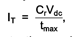
where tmax represents the maximum commutation time, i.e. the time required for completing the commutation process when it is initiated with full load current flowing in the antiparallel diode coupled across one of the main switching devices (Figures 4 and 5). Preferably, the current threshold IT is selected to be sufficiently less than the peak load current such that the sum IT + IB does not exceed the peak load current value. In this way, the addition of the boost current does not result in a device current rating penalty.
Claims (9)
- A method for controlling a power converter of the type including an inverter (10) having at least one phase, said inverter having at least two series-coupled main switching devices (S1,S2) per phase, said series-coupled main switching devices being coupled to positive (p) and negative (n) rails of a dc supply, the junction between said main switching devices being coupled to a load (LF), said main switching devices (S1,S2) each having a snubber capacitor (Cr) coupled in parallel therewith and an antiparallel diode (D₁,D₂) coupled thereacross, said power converter further including a pair of series-coupled bus-splitting capacitors (Cdc) coupled between said positive and negative rails of said dc supply, said power converter further including an auxiliary resonant commutation circuit (12) coupled between the junction joining said main switching devices (S1,S2) and the junction joining said bus-splitting capacitors (Cdc), said auxiliary resonant commutation circuit (12) comprising a pair of antiparallel-coupled auxiliary switching devices (A₁, A₂) coupled in series with a resonant circuit, said resonant circuit including an inductor (Lr) and said snubber capacitors, said method comprising commutating load current between one of said main switching devices (S1,S2) and the opposing one of said antiparallel diodes (D₁, D₂) coupled across the other one of said main switching devices (S1,S2); characterized by ensuring that the output voltage from said resonant circuit at the junction of the main switching devices (S1,S2) attempts to overshoot the rail voltages during each resonant interval by providing a boost current to the current provided by the resonant circuit.
- The method of claim 1, wherein said commutation step is initiated with load current in said opposing one of said antiparallel diodes, by:(a) applying a forcing potential of substantially one-half the dc supply voltage across said inductor (Lr) by turning on one of said auxiliary switching devices (A₁, A₂)(b) allowing current ins aid inductor to increase to the load current level and displace the load current flowing through said opposing one of said antiparallel diodes (D₁, D₂)(c) turning on said other one of said main switching devices (S1,S2) so as to enable the current through said inductor (Lr) to increase to a predetermined boost current threshold above the load current level;(d) turning off said other one of said main switching devices (S₁,S₂) when current therethrough reaches said predetermined boost current threshold, thereby allowing said resonant circuit to resonate from the voltage level of one of said rails of said dc supply to the voltage level of the opposite rail thereof;(e) clamping the output voltage of the respective inverter phase to the voltage level of the opposite rail of said dc supply by forward biasing the other one of said antiparallel diodes (D₁,D₂ );(f) turning one said one of said main switching devices (S₁,S₂) when the voltage thereacross is substantially zero;(g) allowing the current through said inductor (Lr) to decrease to substantially zero; and(h) turning off said one of said auxiliary switching devices (A₁,A₂) when the current therethrough is substantially zero;
whereby the load current flows through said one of said main switching devices (S₁,S₂). - The method of claims 1 wherein said commutation step is initiated with load current in said one of said main switching devices (S₁,S₂), when the load current is less than a high current threshold, by:(a) applying a forcing potential of substantially one-half the dc supply voltage across said inductor (Lr) by turning on one of said auxiliary switching devices (A₁,A₂);(b) allowing current in said inductor (Lr) to increase to a predetermined boost current threshold;(c) turning off said one of said main switching devices (S₁,S₂) when current therethrough reaches said predetermined boost current threshold above the load current level, thereby allowing said resonant circuit to resonate from the voltage level of one of said rails of said dc supply to the voltage level of the opposite rail thereof;(d) clamping the output voltage of the respective inverter phase to the voltage level of the opposite rail of said dc supply by forward biasing said opposing one of said antiparallel diodes (D₁,D₂);(e) allowing the current in said inductor (Lr) to decrease to substantially zero; and(f) turning off said one of said auxiliary switching devices (A₁,A₂) when the current therethrough is substantially zero;
whereby the load current flows through said opposing one of said antiparallel diodes (D₁,D₂). - The method of claim 3 wherein said high current threshold is determined according to the following expression:

- The method of claim 3 wherein said high current threshold is sufficiently less than the peak output current from said inverter such that the sum of said high current threshold and said predetermined boost threshold current does not exceed said peak output current.
- The method of claim 1 wherein said commutation step is initiated with load current in said one of said main switching devices (S₁,S₂), when the load current is greater than a high current threshold, by:(a) turning off said one of said main switching devices (S₁,S₂);(b) allowing the load current to drive the output voltage of the respective inverter phase from the voltage level of one of said rails of said dc supply to the voltage level of the opposite rail thereof;(c) clamping the output voltage of the respective phase of said inverter to the voltage level of the opposite rail of said dc supply by forward biasing said opposing one of said antiparallel diodes (D₁,D₂);
whereby the load current flows through said opposing one of said antiparallel diodes (D₁,D₂). - The method of claim 6 wherein said high current threshold is determined according to the following expression:

- The method of claim 6 wherein said high current threshold is sufficiently less than the peak output current from said inverter such that the sum of said high current threshold and said predetermined boost threshold current does not exceed said peak output current.
- The method of claim 1 wherein said commutation step is initiated with load current in said opposing one of said antiparallel diodes (D₁,D₂), when the load current is greater than a diode boost threshold, by:(a) applying a forcing potential of substantially one-half the dc supply voltage across said inductor (Lr) by turning on one of said auxiliary switching devices (A₁,A₂) ;(b) allowing current in said inductor (Lr) to increase to the load current level and displace the load current flowing through said opposing one of said antiparallel diodes (D₁,D₂);(c) allowing said resonant circuit to resonate from the voltage level of one of said rails of said dc supply to the voltage level of the opposite rail thereof;(d) clamping the output voltage of the respective inverter phase to the voltage level of the opposite rail of said dc supply by forward biasing the other one of said antiparallel diodes (D₁,D₂);(e) turning one said one of said main switching devices (S₁,S₂) when the voltage thereacross is substantially zero;(f) allowing current in said inductor (Lr) to decrease to substantially zero; and(g) turning off said one of said auxiliary switching devices (A₁,A₂) when the current therethrough is substantially zero;
whereby the load current flows through said one of said main switching devices (S₁,S₂).
Applications Claiming Priority (3)
| Application Number | Priority Date | Filing Date | Title |
|---|---|---|---|
| US583910 | 1990-09-17 | ||
| US07/583,910 US5047913A (en) | 1990-09-17 | 1990-09-17 | Method for controlling a power converter using an auxiliary resonant commutation circuit |
| PCT/US1991/003274 WO1992005625A1 (en) | 1990-09-17 | 1991-05-10 | Method for controlling a power converter using an auxiliary resonant commutation circuit |
Publications (2)
| Publication Number | Publication Date |
|---|---|
| EP0500818A1 EP0500818A1 (en) | 1992-09-02 |
| EP0500818B1 true EP0500818B1 (en) | 1995-10-18 |
Family
ID=24335109
Family Applications (1)
| Application Number | Title | Priority Date | Filing Date |
|---|---|---|---|
| EP91909925A Expired - Lifetime EP0500818B1 (en) | 1990-09-17 | 1991-05-10 | Method for controlling a power converter using an auxiliary resonant commutation circuit |
Country Status (11)
| Country | Link |
|---|---|
| US (1) | US5047913A (en) |
| EP (1) | EP0500818B1 (en) |
| JP (1) | JP3037415B2 (en) |
| KR (1) | KR100197825B1 (en) |
| BR (1) | BR9106078A (en) |
| DE (1) | DE69113981T2 (en) |
| ES (1) | ES2079661T3 (en) |
| GR (1) | GR1000904B (en) |
| MX (1) | MX9100234A (en) |
| PT (1) | PT98263B (en) |
| WO (1) | WO1992005625A1 (en) |
Cited By (2)
| Publication number | Priority date | Publication date | Assignee | Title |
|---|---|---|---|---|
| US8947163B2 (en) | 2012-05-02 | 2015-02-03 | Qualcomm Incorporated | Split capacitors scheme for suppressing overshoot voltage glitches in class D amplifier output stage |
| DE102022207036A1 (en) | 2022-07-11 | 2024-01-11 | Friedrich-Alexander-Universität Erlangen-Nürnberg, Körperschaft des öffentlichen Rechts | Method for controlling and switching arrangement for a multi-phase two-point inverter and multi-phase two-point inverter |
Families Citing this family (72)
| Publication number | Priority date | Publication date | Assignee | Title |
|---|---|---|---|---|
| US5172309A (en) * | 1991-08-07 | 1992-12-15 | General Electric Company | Auxiliary quasi-resonant dc link converter |
| US5307004A (en) * | 1992-07-06 | 1994-04-26 | Carsten Bruce W | Soft switching boost and buck regulators |
| US5568368A (en) * | 1993-05-03 | 1996-10-22 | General Electric Company | Square-wave converters with soft voltage transitions for ac power distribution systems |
| WO1995031853A1 (en) * | 1994-05-11 | 1995-11-23 | B & W Loudspeakers Ltd. | Controlled commutator circuit |
| JPH08289561A (en) * | 1995-02-14 | 1996-11-01 | Toshiba Corp | Power converter |
| DE69610000T2 (en) * | 1995-02-14 | 2001-05-17 | Toshiba Kawasaki Kk | Power converter |
| US5684426A (en) * | 1995-12-21 | 1997-11-04 | General Electric Company | GTO gate driver circuits for snubbered and zero voltage soft switching converters |
| US5892673A (en) * | 1996-03-25 | 1999-04-06 | General Electric Company | Robust, high-density, high-efficiency state sequence controller for an auxiliary resonant commutation pole power converter |
| US5710699A (en) * | 1996-05-28 | 1998-01-20 | General Electric Company | Power electronic interface circuits for batteries and ultracapacitors in electric vehicles and battery storage systems |
| US5723956A (en) * | 1996-05-28 | 1998-03-03 | General Electric Company | Low cost electronic ultracapacitor interface technique to provide load leveling of a battery for pulsed load or motor traction drive applications |
| US5684688A (en) * | 1996-06-24 | 1997-11-04 | Reliance Electric Industrial Company | Soft switching three-level inverter |
| US5798633A (en) * | 1996-07-26 | 1998-08-25 | General Electric Company | Battery energy storage power conditioning system |
| US5936855A (en) * | 1996-09-03 | 1999-08-10 | Mercury Electric Corporation | Harmonic correction of 3-phase rectifiers and converters |
| FR2753850B1 (en) * | 1996-09-24 | 1998-11-13 | SOFT SWITCHING POWER CONVERTER COMPRISING MEANS OF CORRECTING THE MEDIUM VOLTAGE OF A CAPACITIVE VOLTAGE DIVIDER | |
| FR2758019B1 (en) * | 1996-12-30 | 1999-01-22 | Alsthom Cge Alcatel | POWER CONVERTER WITH IMPROVED CONTROL OF MAIN SWITCHES |
| US6091615A (en) * | 1997-11-28 | 2000-07-18 | Denso Corporation | Resonant power converter |
| US5898583A (en) * | 1998-02-02 | 1999-04-27 | General Electric Company | Gate drive latching circuit for an auxiliary resonant commutation circuit |
| US6069809A (en) * | 1998-05-08 | 2000-05-30 | Denso Corporation | Resonant inverter apparatus |
| US6865096B1 (en) | 1998-07-09 | 2005-03-08 | Illinois Tool Works Inc. | Power convertor with low loss switching |
| US6115273A (en) * | 1998-07-09 | 2000-09-05 | Illinois Tool Works Inc. | Power converter with low loss switching |
| US6087738A (en) * | 1998-08-20 | 2000-07-11 | Robicon Corporation | Variable output three-phase transformer |
| US6262555B1 (en) | 1998-10-02 | 2001-07-17 | Robicon Corporation | Apparatus and method to generate braking torque in an AC drive |
| US6225862B1 (en) * | 1998-11-13 | 2001-05-01 | Lamda Electronics Inc. | Series resonant circuit with inherent short circuit protection |
| US6268666B1 (en) | 1999-02-25 | 2001-07-31 | Southwest Research Institute | Bi-directional power conversion apparatus for combination of energy sources |
| DE19945864A1 (en) * | 1999-04-20 | 2000-10-26 | Abb Patent Gmbh | ARCP three-point or multi-point converter |
| EP1087512A3 (en) * | 1999-09-02 | 2006-03-08 | ABB PATENT GmbH | ARCP multi-point power converter with intermediate circuit capacitors being voltage variable |
| US20040022073A1 (en) * | 2000-04-03 | 2004-02-05 | Nielsen Stig Munk | Resonant converter having a self inductance |
| US6496388B2 (en) | 2000-04-20 | 2002-12-17 | Fairchild Semiconductor Corporation | Quasi-resonant converter |
| CN1236545C (en) | 2000-04-28 | 2006-01-11 | Tdk股份有限公司 | Power converting device |
| EP1298780B1 (en) * | 2000-05-10 | 2006-11-22 | Hitachi Medical Corporation | X-ray generator and x-ray ct apparatus comprising the same |
| DK174165B1 (en) * | 2000-10-13 | 2002-08-05 | American Power Conversion Denm | resonance |
| SE521885C2 (en) * | 2001-04-11 | 2003-12-16 | Abb Ab | DC Drives |
| JP2002325464A (en) | 2001-04-26 | 2002-11-08 | Honda Motor Co Ltd | Resonant inverter circuit |
| US6570780B2 (en) | 2001-05-17 | 2003-05-27 | Honda Giken Kogyo Kabushiki Kaisha | Resonant inverter control system |
| SE522427C2 (en) * | 2001-05-30 | 2004-02-10 | Abb Ab | Converter device and method for controlling such |
| US6646407B2 (en) * | 2001-06-08 | 2003-11-11 | General Motors Corporation | Electric motor control having DC-DC converter and method of using same |
| SE523487C2 (en) * | 2001-07-16 | 2004-04-20 | Abb Ab | Procedure for controlling a rectifier |
| KR100896139B1 (en) | 2001-08-13 | 2009-05-12 | 인덕토썸코오퍼레이션. | Fault tolerant power supply circuit |
| US6570370B2 (en) * | 2001-08-21 | 2003-05-27 | Raven Technology, Llc | Apparatus for automatic tuning and control of series resonant circuits |
| SE524447C2 (en) * | 2002-08-08 | 2004-08-10 | Abb Ab | Converters and method of controlling them |
| JP2008512082A (en) * | 2004-08-30 | 2008-04-17 | アドバンスト・エナジー・インダストリーズ・インコーポレイテッド | Bipolar power supply with lossless snubber |
| US7126833B2 (en) * | 2004-11-24 | 2006-10-24 | Ut-Battelle, Llc | Auxiliary quasi-resonant dc tank electrical power converter |
| US7602157B2 (en) | 2005-12-28 | 2009-10-13 | Flyback Energy, Inc. | Supply architecture for inductive loads |
| US8672732B2 (en) * | 2006-01-19 | 2014-03-18 | Schneider Electric It Corporation | Cooling system and method |
| CN101755495B (en) | 2007-05-15 | 2013-10-16 | 美国能量变换公司 | Methods and systems for managing facility power and cooling |
| CN101388612B (en) * | 2007-09-14 | 2011-08-31 | 力博特公司 | Soft switch circuit controlling method in switch power source |
| WO2009039305A2 (en) * | 2007-09-18 | 2009-03-26 | Flyback Energy, Inc. | Current waveform construction to generate ac power with low harmonic distortion from localized energy sources |
| US8116105B2 (en) | 2008-02-07 | 2012-02-14 | American Power Conversion Corporation | Systems and methods for uninterruptible power supply control |
| US7881079B2 (en) * | 2008-03-24 | 2011-02-01 | American Power Conversion Corporation | UPS frequency converter and line conditioner |
| JP5228886B2 (en) * | 2008-09-05 | 2013-07-03 | 富士電機株式会社 | Snubber circuit |
| WO2010125630A1 (en) | 2009-04-27 | 2010-11-04 | 東芝三菱電機産業システム株式会社 | Power converter |
| US8228046B2 (en) * | 2009-06-16 | 2012-07-24 | American Power Conversion Corporation | Apparatus and method for operating an uninterruptible power supply |
| EP2482440B1 (en) * | 2009-09-24 | 2017-10-11 | Toshiba Mitsubishi-Electric Industrial Systems Corporation | Power conversion device |
| US8503201B2 (en) | 2009-12-03 | 2013-08-06 | Schneider Electric It Corporation | Transient clamping circuitry for voltage converter |
| WO2011082188A1 (en) * | 2009-12-28 | 2011-07-07 | Flyback Energy Inc. | External field interaction motor |
| CA2785715A1 (en) * | 2009-12-28 | 2011-07-28 | Paul M. Babcock | Controllable universal supply with reactive power management |
| DE102010014142A1 (en) * | 2010-04-07 | 2011-10-13 | Alpitronic Gmbh | Commutation method, commutation circuit and electrical energy converter |
| US8878389B2 (en) | 2011-01-11 | 2014-11-04 | Schneider Electric It Corporation | Method and apparatus for providing uninterruptible power |
| DE202011050665U1 (en) | 2011-07-07 | 2012-10-09 | Alpitronic Gmbh | Commutation circuit and electrical energy converter |
| US8884464B2 (en) | 2011-08-29 | 2014-11-11 | Schneider Electric It Corporation | Twin boost converter with integrated charger for UPS system |
| US9952103B2 (en) | 2011-12-22 | 2018-04-24 | Schneider Electric It Corporation | Analysis of effect of transient events on temperature in a data center |
| AU2011383606A1 (en) | 2011-12-22 | 2014-07-17 | Schneider Electric It Corporation | System and method for prediction of temperature values in an electronics system |
| JP2013215043A (en) * | 2012-04-02 | 2013-10-17 | Fuji Electric Co Ltd | Multilevel power converter |
| SE537227C2 (en) * | 2012-07-06 | 2015-03-10 | Comsys Ab | resonant Converters |
| SE537080C2 (en) | 2012-07-06 | 2014-12-30 | Comsys Ab | Improved switch protection for resonant inverters |
| WO2014032302A1 (en) | 2012-09-03 | 2014-03-06 | Schneider Electric It Corporation | Method and apparatus for controlling distribution of power |
| CN105191091A (en) * | 2013-01-11 | 2015-12-23 | 阿尔斯通技术有限公司 | Voltage source converter |
| EP2800265A1 (en) | 2013-05-03 | 2014-11-05 | ALSTOM Technology Ltd | Converter |
| WO2015069917A1 (en) * | 2013-11-07 | 2015-05-14 | Rompower Energy System, Inc. | Bridgeless pfc using single sided high frequency switching |
| EP2887529A1 (en) | 2013-12-23 | 2015-06-24 | Alstom Technology Ltd | Modular multilevel converter leg with flat-top PWM modulation, converter and hybrid converter topologies |
| FR3068547B1 (en) * | 2017-06-30 | 2019-08-16 | Stmicroelectronics (Tours) Sas | THYRISTORS REVERSIBLE AC / DC CONVERTER |
| US11469684B2 (en) * | 2020-06-11 | 2022-10-11 | Abb Schweiz Ag | Active damping of soft switching resonant converters |
Family Cites Families (7)
| Publication number | Priority date | Publication date | Assignee | Title |
|---|---|---|---|---|
| US4173779A (en) * | 1978-12-08 | 1979-11-06 | Westinghouse Electric Corp. | Single-pole commutation circuit |
| SE7900490L (en) * | 1979-01-19 | 1980-07-20 | Asea Ab | VEXELRIKTARKOPPLING |
| US4255783A (en) * | 1979-05-30 | 1981-03-10 | United Technologies Corporation | Selective commutation circuit for an inverter |
| US4286317A (en) * | 1979-08-16 | 1981-08-25 | Bbc Brown, Boveri & Co. Ltd. | Forced commutation power converter arrangement in reverse voltage free circuit configuration |
| US4336585A (en) * | 1980-12-23 | 1982-06-22 | United Technologies Corporation | Selective commutation for an inverter |
| US4730242A (en) * | 1986-09-25 | 1988-03-08 | Wisconsin Alumni Research Foundation | Static power conversion and apparatus having essentially zero switching losses |
| DE3743436C1 (en) * | 1987-12-21 | 1989-05-11 | Siemens Ag | Switch-relieved, low-loss three-point inverter |
-
1990
- 1990-09-17 US US07/583,910 patent/US5047913A/en not_active Expired - Lifetime
-
1991
- 1991-05-10 ES ES91909925T patent/ES2079661T3/en not_active Expired - Lifetime
- 1991-05-10 KR KR1019920701162A patent/KR100197825B1/en not_active IP Right Cessation
- 1991-05-10 JP JP03509868A patent/JP3037415B2/en not_active Expired - Lifetime
- 1991-05-10 DE DE69113981T patent/DE69113981T2/en not_active Expired - Fee Related
- 1991-05-10 WO PCT/US1991/003274 patent/WO1992005625A1/en active IP Right Grant
- 1991-05-10 BR BR919106078A patent/BR9106078A/en not_active IP Right Cessation
- 1991-05-10 EP EP91909925A patent/EP0500818B1/en not_active Expired - Lifetime
- 1991-06-21 GR GR910100272A patent/GR1000904B/en not_active IP Right Cessation
- 1991-07-09 PT PT98263A patent/PT98263B/en active IP Right Grant
- 1991-07-16 MX MX9100234A patent/MX9100234A/en unknown
Cited By (3)
| Publication number | Priority date | Publication date | Assignee | Title |
|---|---|---|---|---|
| US8947163B2 (en) | 2012-05-02 | 2015-02-03 | Qualcomm Incorporated | Split capacitors scheme for suppressing overshoot voltage glitches in class D amplifier output stage |
| DE102022207036A1 (en) | 2022-07-11 | 2024-01-11 | Friedrich-Alexander-Universität Erlangen-Nürnberg, Körperschaft des öffentlichen Rechts | Method for controlling and switching arrangement for a multi-phase two-point inverter and multi-phase two-point inverter |
| WO2024013007A1 (en) | 2022-07-11 | 2024-01-18 | Friedrich-Alexander-Universität Erlangen-Nürnberg | Arcp 2-point inverter with only one inductor for several phases, and method for collision-free operation |
Also Published As
| Publication number | Publication date |
|---|---|
| GR1000904B (en) | 1993-03-16 |
| JPH05502365A (en) | 1993-04-22 |
| ES2079661T3 (en) | 1996-01-16 |
| DE69113981D1 (en) | 1995-11-23 |
| JP3037415B2 (en) | 2000-04-24 |
| WO1992005625A1 (en) | 1992-04-02 |
| BR9106078A (en) | 1993-02-02 |
| MX9100234A (en) | 1992-06-05 |
| PT98263B (en) | 1999-01-29 |
| DE69113981T2 (en) | 1996-05-30 |
| KR100197825B1 (en) | 1999-06-15 |
| PT98263A (en) | 1993-08-31 |
| KR920702569A (en) | 1992-09-04 |
| US5047913A (en) | 1991-09-10 |
| EP0500818A1 (en) | 1992-09-02 |
| GR910100272A (en) | 1992-09-11 |
Similar Documents
| Publication | Publication Date | Title |
|---|---|---|
| EP0500818B1 (en) | Method for controlling a power converter using an auxiliary resonant commutation circuit | |
| US5633793A (en) | Soft switched three-phase boost rectifiers and voltage source inverters | |
| De Doncker et al. | The auxiliary resonant commutated pole converter | |
| US6603675B1 (en) | Apparatus and a method for voltage conversion | |
| US7869226B2 (en) | Achieving ZVS in a two quadrant converter using a simplified auxiliary circuit | |
| Cuadros et al. | Space vector modulated, zero-voltage transition three-phase to DC bidirectional converter | |
| US7417409B2 (en) | Power losses reduction in switching power converters | |
| US4805082A (en) | Regenerative two-quadrant converter | |
| JPH07222444A (en) | Dc-dc converter | |
| Norrga et al. | A three-phase soft-switched isolated AC/DC converter without auxiliary circuit | |
| Ghodke et al. | ZVZCS, dual, two-transistor forward DC-DC converter with peak voltage of Vin/2, high input and high power application | |
| JP2002238257A (en) | Control method for resonance dc-dc converter | |
| Teichmann et al. | ARCP soft-switching technique in matrix converters | |
| Pal et al. | A pwm zvs high-frequency-link three-phase inverter with t-type npc unfolder | |
| Ishikawa et al. | A novel soft-switched PWM current source inverter with voltage clamped circuit | |
| US5870292A (en) | Series resonant converter for switched reluctance motor drive | |
| Bornhardt | Novel soft-switched GTO-inverter circuits | |
| Ishida et al. | Real-time output voltage control method of quasi-ZCS series resonant HF-linked DC-AC converter | |
| Holtz et al. | High-power pulsewidth controlled current source GTO inverter for high switching frequency | |
| Elasser et al. | Soft switching active snubbers for dc/ac converters | |
| Williams et al. | Passive snubber energy recovery for a GTO thyristor inverter bridge leg | |
| JP2555621B2 (en) | Inverter energy recovery circuit | |
| da Silva et al. | A current clamping circuit for a PWM series resonant DC link power converter | |
| Nomura et al. | A New Method of Forced Commutation for Thyristor Converters Having AC Source Inductance | |
| McMurray | THE EARLY DEVELOPMENT OF FORCE-COMMUTATED THYRISTOR INVERTERS |
Legal Events
| Date | Code | Title | Description |
|---|---|---|---|
| PUAI | Public reference made under article 153(3) epc to a published international application that has entered the european phase |
Free format text: ORIGINAL CODE: 0009012 |
|
| 17P | Request for examination filed |
Effective date: 19920414 |
|
| AK | Designated contracting states |
Kind code of ref document: A1 Designated state(s): BE DE ES FR GB IT NL |
|
| 17Q | First examination report despatched |
Effective date: 19940323 |
|
| GRAA | (expected) grant |
Free format text: ORIGINAL CODE: 0009210 |
|
| AK | Designated contracting states |
Kind code of ref document: B1 Designated state(s): BE DE ES FR GB IT NL |
|
| ET | Fr: translation filed | ||
| REF | Corresponds to: |
Ref document number: 69113981 Country of ref document: DE Date of ref document: 19951123 |
|
| ITF | It: translation for a ep patent filed |
Owner name: SAIC BREVETTI S.R.L. |
|
| REG | Reference to a national code |
Ref country code: ES Ref legal event code: FG2A Ref document number: 2079661 Country of ref document: ES Kind code of ref document: T3 |
|
| PLBE | No opposition filed within time limit |
Free format text: ORIGINAL CODE: 0009261 |
|
| STAA | Information on the status of an ep patent application or granted ep patent |
Free format text: STATUS: NO OPPOSITION FILED WITHIN TIME LIMIT |
|
| 26N | No opposition filed | ||
| REG | Reference to a national code |
Ref country code: GB Ref legal event code: IF02 |
|
| PGFP | Annual fee paid to national office [announced via postgrant information from national office to epo] |
Ref country code: FR Payment date: 20020417 Year of fee payment: 12 |
|
| PGFP | Annual fee paid to national office [announced via postgrant information from national office to epo] |
Ref country code: DE Payment date: 20020520 Year of fee payment: 12 |
|
| PGFP | Annual fee paid to national office [announced via postgrant information from national office to epo] |
Ref country code: BE Payment date: 20020527 Year of fee payment: 12 |
|
| PGFP | Annual fee paid to national office [announced via postgrant information from national office to epo] |
Ref country code: ES Payment date: 20020606 Year of fee payment: 12 |
|
| PGFP | Annual fee paid to national office [announced via postgrant information from national office to epo] |
Ref country code: NL Payment date: 20030423 Year of fee payment: 13 |
|
| PGFP | Annual fee paid to national office [announced via postgrant information from national office to epo] |
Ref country code: GB Payment date: 20030507 Year of fee payment: 13 |
|
| PG25 | Lapsed in a contracting state [announced via postgrant information from national office to epo] |
Ref country code: ES Free format text: LAPSE BECAUSE OF NON-PAYMENT OF DUE FEES Effective date: 20030512 |
|
| PG25 | Lapsed in a contracting state [announced via postgrant information from national office to epo] |
Ref country code: BE Free format text: LAPSE BECAUSE OF NON-PAYMENT OF DUE FEES Effective date: 20030531 |
|
| BERE | Be: lapsed |
Owner name: *GENERAL ELECTRIC CY Effective date: 20030531 |
|
| PG25 | Lapsed in a contracting state [announced via postgrant information from national office to epo] |
Ref country code: DE Free format text: LAPSE BECAUSE OF NON-PAYMENT OF DUE FEES Effective date: 20031202 |
|
| PG25 | Lapsed in a contracting state [announced via postgrant information from national office to epo] |
Ref country code: FR Free format text: LAPSE BECAUSE OF NON-PAYMENT OF DUE FEES Effective date: 20040130 |
|
| REG | Reference to a national code |
Ref country code: FR Ref legal event code: ST |
|
| PG25 | Lapsed in a contracting state [announced via postgrant information from national office to epo] |
Ref country code: GB Free format text: LAPSE BECAUSE OF NON-PAYMENT OF DUE FEES Effective date: 20040510 |
|
| REG | Reference to a national code |
Ref country code: ES Ref legal event code: FD2A Effective date: 20030512 |
|
| PG25 | Lapsed in a contracting state [announced via postgrant information from national office to epo] |
Ref country code: NL Free format text: LAPSE BECAUSE OF NON-PAYMENT OF DUE FEES Effective date: 20041201 |
|
| GBPC | Gb: european patent ceased through non-payment of renewal fee |
Effective date: 20040510 |
|
| NLV4 | Nl: lapsed or anulled due to non-payment of the annual fee |
Effective date: 20041201 |
|
| PG25 | Lapsed in a contracting state [announced via postgrant information from national office to epo] |
Ref country code: IT Free format text: LAPSE BECAUSE OF NON-PAYMENT OF DUE FEES;WARNING: LAPSES OF ITALIAN PATENTS WITH EFFECTIVE DATE BEFORE 2007 MAY HAVE OCCURRED AT ANY TIME BEFORE 2007. THE CORRECT EFFECTIVE DATE MAY BE DIFFERENT FROM THE ONE RECORDED. Effective date: 20050510 |