EP0476543A2 - Liquid crystal alignment film and method of manufacturing the same - Google Patents
Liquid crystal alignment film and method of manufacturing the same Download PDFInfo
- Publication number
- EP0476543A2 EP0476543A2 EP91115590A EP91115590A EP0476543A2 EP 0476543 A2 EP0476543 A2 EP 0476543A2 EP 91115590 A EP91115590 A EP 91115590A EP 91115590 A EP91115590 A EP 91115590A EP 0476543 A2 EP0476543 A2 EP 0476543A2
- Authority
- EP
- European Patent Office
- Prior art keywords
- liquid crystal
- alignment film
- crystal alignment
- silane
- carbon chains
- Prior art date
- Legal status (The legal status is an assumption and is not a legal conclusion. Google has not performed a legal analysis and makes no representation as to the accuracy of the status listed.)
- Granted
Links
- 0 CCCC(C)C(OC(CC1)CCC1O*)=O Chemical compound CCCC(C)C(OC(CC1)CCC1O*)=O 0.000 description 3
Images


Classifications
-
- G—PHYSICS
- G02—OPTICS
- G02F—OPTICAL DEVICES OR ARRANGEMENTS FOR THE CONTROL OF LIGHT BY MODIFICATION OF THE OPTICAL PROPERTIES OF THE MEDIA OF THE ELEMENTS INVOLVED THEREIN; NON-LINEAR OPTICS; FREQUENCY-CHANGING OF LIGHT; OPTICAL LOGIC ELEMENTS; OPTICAL ANALOGUE/DIGITAL CONVERTERS
- G02F1/00—Devices or arrangements for the control of the intensity, colour, phase, polarisation or direction of light arriving from an independent light source, e.g. switching, gating or modulating; Non-linear optics
- G02F1/01—Devices or arrangements for the control of the intensity, colour, phase, polarisation or direction of light arriving from an independent light source, e.g. switching, gating or modulating; Non-linear optics for the control of the intensity, phase, polarisation or colour
- G02F1/13—Devices or arrangements for the control of the intensity, colour, phase, polarisation or direction of light arriving from an independent light source, e.g. switching, gating or modulating; Non-linear optics for the control of the intensity, phase, polarisation or colour based on liquid crystals, e.g. single liquid crystal display cells
- G02F1/133—Constructional arrangements; Operation of liquid crystal cells; Circuit arrangements
- G02F1/1333—Constructional arrangements; Manufacturing methods
- G02F1/1337—Surface-induced orientation of the liquid crystal molecules, e.g. by alignment layers
- G02F1/133711—Surface-induced orientation of the liquid crystal molecules, e.g. by alignment layers by organic films, e.g. polymeric films
- G02F1/133719—Surface-induced orientation of the liquid crystal molecules, e.g. by alignment layers by organic films, e.g. polymeric films with coupling agent molecules, e.g. silane
-
- B—PERFORMING OPERATIONS; TRANSPORTING
- B05—SPRAYING OR ATOMISING IN GENERAL; APPLYING FLUENT MATERIALS TO SURFACES, IN GENERAL
- B05D—PROCESSES FOR APPLYING FLUENT MATERIALS TO SURFACES, IN GENERAL
- B05D1/00—Processes for applying liquids or other fluent materials
- B05D1/18—Processes for applying liquids or other fluent materials performed by dipping
- B05D1/185—Processes for applying liquids or other fluent materials performed by dipping applying monomolecular layers
-
- B—PERFORMING OPERATIONS; TRANSPORTING
- B82—NANOTECHNOLOGY
- B82Y—SPECIFIC USES OR APPLICATIONS OF NANOSTRUCTURES; MEASUREMENT OR ANALYSIS OF NANOSTRUCTURES; MANUFACTURE OR TREATMENT OF NANOSTRUCTURES
- B82Y30/00—Nanotechnology for materials or surface science, e.g. nanocomposites
-
- B—PERFORMING OPERATIONS; TRANSPORTING
- B82—NANOTECHNOLOGY
- B82Y—SPECIFIC USES OR APPLICATIONS OF NANOSTRUCTURES; MEASUREMENT OR ANALYSIS OF NANOSTRUCTURES; MANUFACTURE OR TREATMENT OF NANOSTRUCTURES
- B82Y40/00—Manufacture or treatment of nanostructures
-
- C—CHEMISTRY; METALLURGY
- C09—DYES; PAINTS; POLISHES; NATURAL RESINS; ADHESIVES; COMPOSITIONS NOT OTHERWISE PROVIDED FOR; APPLICATIONS OF MATERIALS NOT OTHERWISE PROVIDED FOR
- C09K—MATERIALS FOR MISCELLANEOUS APPLICATIONS, NOT PROVIDED FOR ELSEWHERE
- C09K2323/00—Functional layers of liquid crystal optical display excluding electroactive liquid crystal layer characterised by chemical composition
- C09K2323/02—Alignment layer characterised by chemical composition
- C09K2323/023—Organic silicon compound, e.g. organosilicon
Definitions
- This invention relates to a liquid crystal alignment film using a specific monomolecular film, a method of manufacturing the same, a liquid crystal display apparatus and a method of manufacturing the same.
- the invention concerns a liquid crystal alignment film used for plane liquid crystal display panels for displaying TV images and computer images, a method of manufacturing the same liquid crystal alignment film, a liquid crystal display apparatus using the same film and a method of manufacturing the same film.
- the alignment film is necessary for conventional liquid crystal elements such as monochromatic and color liquid crystal elements.
- the prior art color liquid crystal display panel has a structure, in which a liquid crystal is sealed between two substrates provided with opposed matrix array electrodes via liquid crystal alignment films formed by coating polyvinyl alcohol or polyimide with a spinner (i.e., by centrifugal spin coating).
- Figure 8 shows such a prior art color liquid crystal display panel.
- the apparatus has a first glass substrate 31 provided with a TFT (thin-film transistor) array 33 with pixel electrodes 32 and a second glass substrate 34 provided with pluralities of red, blue and green color filters 35,and transparent electrode 36.
- Liquid crystal alignment films 37 are then formed on top of the layers previously applied to glass substrate 31 and 34 by coating the substrates with polyvinyl alcohol or polyimide using a spinner and then polishing (or rubbing). These coated substrates are then assembled together by sealing them with adhesive 39 with a spacer 38 interposed between them. The sealed space is filled with twisted nematic (TN) liquid crystal 40 or the like, thus obtaining a panel structure.
- Polarizer 41 and 42 are disposed on the front and back sides of the panel, respectively.
- a color image is displayed on the apparatus in the direction of arrow A by operating TFT array 33 while illuminating the apparatus with backlight 43.
- the alignment film is also necessary for other ferroelectric liquid crystals.
- the alignment film is produced by dissolving a resin such as polyvinyl alcohol or polyimide in an organic solvent, coating the solution by a rotational (or spin) coating method or the like and then polishing using a felt cloth or the like. Therefore, it is difficult to obtain uniform coating of an alignment film in the case of a large area panel (for instance a 14-inch display).
- the coating thickness is on the order of several microns. This results in great performance deterioration in the case of a display panel requiring an alignment film with a thickness of the order of 100 nm such as ferroelectric liquid crystals.
- the present invention seeks to solve the above problems in the prior art, and it provides a liquid crystal alignment film, a method of manufacturing the same film, a liquid crystal display apparatus and a method of manufacturing the same apparatus, which all use a particular monomolecular film permitting highly effective formation of an alignment film used for liquid crystal display panels.
- the film is produced uniformly and thinly without the need for polishing (or rubbing).
- a liquid crystal alignment film which comprises a monomolecular film including straight chains directly or indirectly chemically adsorbed at one end to an electrode via -Si-O- bonds and crosslinked in a state of alignment in a particular direction.
- a liquid crystal alignment film which comprises the steps of: causing simultaneous chemical adsorption of: a silane-based surface active agent having intramolecular dipoles and containing polymerizable groups in a non-aquaous organic solvent; or a plurality of different silane-based surface active agents containing polymerizable groups and mixed with the first-mentioned silane-based surface active agent; on a predetermined substrate surface formed with an electrode, in order to chemically couple silicon groups of the active agent or agents thereby forming a monomolecular film on the substrate surface; and irradiating the adsorbed silane-based surface active agent or agents with an energy beam while the agent or agents are aliqned in a magnetic or electric field, to cause reaction of the polymerizable groups and thus effect crosslinking thereof, thereby effecting alignment and fixing of the adsorbed silane-based surface active agent or agents.
- a liquid crystal display apparatus which comprises a pair of opposed electrodes, a liquid crystal alignment film formed on at least one of the electrodes and a liquid crystal provided between the opposed electrodes, the liquid crystal alignment film comprising a monomolecular film having straight carbon chains, the straight carbon chains having one end directly or indirectly chemically adsorbed to an electrode via a -Si-O- bond (covalent bond) and being crosslinked in a state of alignment in a particular direction.
- a method of manufacturing a liquid crystal display apparatus which comprises the steps of:
- the liquid crystal alignment film according to the invention has a structure consisting of a monomolecular film including straight carbon chains directly or indirectly chemically adsorbed at one end to an electrode via a -Si-O- bond and crosslinked in a state of alignment in a particular direction. It is thus possible to produce a high quality alignment film used for a liquid crystal display panel without polishing (or rubbing).
- a chemically adsorbed monomolecular film can be polymerized in an aligned state in an electric or magnetic field.
- the liquid crystal alignment film noted above thus can be produced highly efficiently, thinly and uniformly.
- liquid crystal display apparatus according to the invention, a high performance display panel using the liquid crystal alignment film noted above can be manufactured at low cost.
- the high performance display panel can be manufactured easily and efficiently.
- Figures 1(a) is a greatly enlarged cross sectional view of an uncrosslinked monomolecular layer according to the present invention.
- Figures 1(b) is a greatly enlarged cross sectional view of a cross linked monomolecular layer according to the present invention.
- Figures 2 is a greatly enlarged schematic cross sectional view of a crosslinked monomolecular layer according to the present invention.
- Figure 3(a) is a greatly enlarged cross sectional view of an uncrosslinked monomolecular layer according to the present invention.
- Figure 3(b) is a greatly enlarged cross sectional view of a crosslinked monomolecular layer according to the present invention.
- Figure 4 is a greatly enlarged schematic cross sectional view of a crosslinked monomolecular layer according to the present invention.
- Figure 5(a) is a greatly enlarged cross sectional view of an uncrosslinked monomolecular layer according to the present invention.
- Figure 5(b) is a greatly enlarged cross sectional view of a crosslinked monomolecular layer according to the present invention.
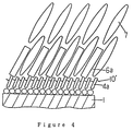
- Figure 6 is a greatly enlarged schematic cross sectional view of a crosslinked monomolecular layer according to the present invention.
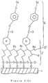
- Figure 7 is a schematic cross sectional view of a liquid crystal display device having alignment films according to the present invention.
- Figure 8 is a schematic cross sectional view of a liquid crystal display device using prior art alignment films.
- Figures 1 to 7 show an embodiment of the invention.
- a hydrophilic substrate 1 for instance glass, ITO (Indium Tin Oxide), or quartz having -OH groups at the surface
- a silane surface active agent containing polymerizable groups and having intramolecular dipoles by a chemical adsorption method.
- the polymerizable groups are then polymerized by irradiating with an energy beam (for instance, electron beam, alpha ( ⁇ ) rays, gamma ( ⁇ ) rays or ultraviolet (UV) rays) while the molecules of the surface active agent are held aligned (for instance tilted by an angle of 0.5 degree) in an electric field (of about 1 x 10⁷ V/cm) or a magnetic field (of about 1 Tesla), thus forming an adsorbed monomolecular polymerized film 2' comprising the silane surface active agent aligned in a fixed direction.
- an energy beam for instance, electron beam, alpha ( ⁇ ) rays, gamma ( ⁇ ) rays or ultraviolet (UV) rays
- an energy beam for instance, electron beam, alpha ( ⁇ ) rays, gamma ( ⁇ ) rays or ultraviolet (UV) rays
- an energy beam for instance, electron beam, alpha ( ⁇ ) rays, gam
- diacetylene (-C ⁇ C-C ⁇ C-) groups are capable of undergoing a topochemical polymerizing reaction (polymerization on a surface) when irradiated with ultraviolet rays and are thus more convenient for the present invention.
- composition ratio of the silane-based surface active agent between the long straight carbon chains and short carbon chains is suitably anywhere from 1 : 0 to 1 : 10.
- This composition is dissolved in a mixtured solvent at a concentration of 2 x 10 ⁇ 3 to 5 x 10 ⁇ 2 Mol/l.
- the mixtured solvent are containing 80 wt% n-hexane, 12 wt% carbon tetrachloride and 8 wt% chloroform. And the substate 1 is dipped in the solution. At this time, the surface of substrate 1 has a hydrophilic surface containing -OH groups.
- the adsorbed monomolecular film 2 comprising the silane surface active agent is formed as a single layer (with a thickness of 1 to 3 nm) on the substrate surface.
- a molecule design is provided such that the vinyl groups 10 in the two different surface active molecules noted above have the same height level in the monomolecular film.
- any suitable chemical adsorption material may be used provided it includes group capable of bonding with an -OH group (for instance an -SiCl group).
- a silane-based surface active agent which contains long straight carbon chains with a portion thereof replaced with substitute groups ( R 1) and the other end constituted by trichlorosilane groups
- a silane-based surface active agent which contains short carbon chains with a portion thereof replaced with substitute groups and the other end constituted by trichlorosilane groups
- a silane-based surface active agent which contains polymerizable groups and to which are coupled liquid crystal molecules (for instance a nematic liquid crystal portion 6 shown in Figure 3) similar to the sealed liquid crystal as a portion of substute groups; and (2) a silane-based surface active agent having short carbon chains and polymerizable groups; followed by adsorption and polymerization in the manner described above, an alignment film can be obtained, which has excellent alignment characteristics particularly with respect to a specific sealed liquid crystal.
- R 3 represents a usual hydrocarbon chain substitute group or H.
- sealed compounds of the liquid crystal molecules contain a ferroelectric liquid crystal
- a surface-based surface active agent with ferroelectric liquid crystal portion 8 coupled thereto and a silane-based surface active agent having short carbon chains are adsorbed in a predetermined composition ratio.
- ferroelectric liquid crystal liquid crystals based on azomethine, azoxys or ester.
- the ferroelectric liquid crystal is brought into contact with the substrate provided with an alignment film having the ferroelectyric liquid crystal 8
- the molecules of the ferroelectric liquid crystal 9 as shown in Figure 6 enter the interstices among the ferroelectric liquid crystal portion 8a of the adsorbed monomolecular film.
- Schematically shown at 4a and 8a are short carbon chains 4 and ferroelectric liquid crystal portion 8 shown in Figure 5 (a) and 5(b).
- liquid crystal alignment film i.e., (1) one which is obtained by simultaneously chemically adsorbing a plurality of different silane-based surface active agents mixed in predetermined proportions and having polymerizable groups; and (2) one which is produced by a monomolecular film obtained by causing adsorption in a predetermined composition ratio of a silane-based surface active agent with liquid crystal molecules coupled thereto and a silane-based surface active agents having short carbon chains, and causing polymerization of the polymerizable groups in a state of alignment in an electric or magnetic field, thereby effecting the crosslinking and fixing of the adsorbed molecules.
- liquid crystal alignment film is produced by adsorption from a single silane-based surface active agent containng straight carbon chains and polymerizable groups, followed by polymerization and fixing in a vertically aligned state, it is possible to obtain a liquid crystal alignment film, which permits substantially vertical alignment of the liquid crystal.
- a liquid crystal display device can be manufactured as follows. As shown in Figure 7, a first substrate 13 is provided with a first electrode group 11 in a matrix array and also with a transistor group 12 for driving the electrode group. A second substrate 16 is provided with a color filter group 14 opposing the first electrode group and a second electrode 15. Thereafter, a silane-based surface-active agent is chemically adsorbed on one or both electrodes either directly or indirectly via an insulating film in a nonaquaous organic solvent (e.g., n-cetane as n-paraffin, which permits efficient control of long molecular alignment).
- a nonaquaous organic solvent e.g., n-cetane as n-paraffin, which permits efficient control of long molecular alignment.
- Silicon in the active agent and a natural oxide film on the substrate surface are thus chemically bonded to form a monomolecular film which will become a liquid crystal alignment film. Then, polymerizaition is effected with the film in a state of alignment. Afterwards, the first and second substrates 13 and 16 are positioned such that they oppose each other and are secured together with a spacer 18 interposed between then using adhesive 19. Then a predetermined liquid crystal 20 is injected into the space between the substrates. The system thus obtained is then combined with polarizer plates 21 and 22 to complete the device. With this device, a video image can be displayed in the direction of arrow A by driving the individual transistors using a video signal while illuminating the entire surface with backlight 23.
- a liquid crystal alignment film is manufactured by causing chemical adsorption as a monomolecular layer of a silane-based surface active agent directly or indirectly on electrode surface and then causing polymerization in a state of alignment.
- polishing or rubbing is unnecessary, and the alignment film can be obtained highly efficiently, thinly and uniformly.
- the adsorbed alignment film may be coupled a specific liquid crystal, e.g., nematic liquid crystal or ferromagnetic liquid crystal.
- a specific liquid crystal e.g., nematic liquid crystal or ferromagnetic liquid crystal.
- the insulating film intervening between the liquid crystal and electrode is very thin, and thus it is possible to reduce the energy for driving the liquid crystal display device.
- the liquid crystal alignment film according to the invention comprises a monomolecular film including straight carbon chains, which are directly or indirectly chemically adsorbed at one end to an electride via -Si-O- bonds and cross linked while aligned in a particular direction.
- a high quality alignment film used for a liquid crystal display panel can be obtained without the polishing (or rubbing).
- the polymerizaiton can be carried out with the chemically adsorbed monomolecular film aligned under an electric or magnetic field, thus permitting formation of the liquid crystal alignment film highly efficiently, thinly and uniformly.
- liquid crystal display apparatus Furthermore, with the liquid crystal display apparatus according to the invention, a high performance display panel using the liquid crystal can be manufactured at a low cost.
- the high performance display panel can be manufactured logically and efficiently.
Abstract
Description
- This invention relates to a liquid crystal alignment film using a specific monomolecular film, a method of manufacturing the same, a liquid crystal display apparatus and a method of manufacturing the same.
- More specifically, the invention concerns a liquid crystal alignment film used for plane liquid crystal display panels for displaying TV images and computer images, a method of manufacturing the same liquid crystal alignment film, a liquid crystal display apparatus using the same film and a method of manufacturing the same film.
- With a liquid crystal display apparatus, it is necessary to provide an alignment film between the electrode surface and the liquid crystal composition in order to obtain normal operation with application of an electric field to the liquid crystal composition. The alignment film is necessary for conventional liquid crystal elements such as monochromatic and color liquid crystal elements.
- A conventional color liquid crystal display panel will now be described.
- The prior art color liquid crystal display panel has a structure, in which a liquid crystal is sealed between two substrates provided with opposed matrix array electrodes via liquid crystal alignment films formed by coating polyvinyl alcohol or polyimide with a spinner (i.e., by centrifugal spin coating).
- Figure 8 shows such a prior art color liquid crystal display panel. As shown, the apparatus has a
first glass substrate 31 provided with a TFT (thin-film transistor)array 33 withpixel electrodes 32 and asecond glass substrate 34 provided with pluralities of red, blue andgreen color filters 35,andtransparent electrode 36. Liquidcrystal alignment films 37 are then formed on top of the layers previously applied toglass substrate spacer 38 interposed between them. The sealed space is filled with twisted nematic (TN)liquid crystal 40 or the like, thus obtaining a panel structure. Polarizer 41 and 42 are disposed on the front and back sides of the panel, respectively. A color image is displayed on the apparatus in the direction of arrow A by operatingTFT array 33 while illuminating the apparatus withbacklight 43. - The alignment film is also necessary for other ferroelectric liquid crystals.
- However, in the prior art the alignment film is produced by dissolving a resin such as polyvinyl alcohol or polyimide in an organic solvent, coating the solution by a rotational (or spin) coating method or the like and then polishing using a felt cloth or the like. Therefore, it is difficult to obtain uniform coating of an alignment film in the case of a large area panel (for instance a 14-inch display). In addition, with rotational coating the coating thickness is on the order of several microns. This results in great performance deterioration in the case of a display panel requiring an alignment film with a thickness of the order of 100 nm such as ferroelectric liquid crystals. For example, it is difficult to obtain a thin and uniformly thick coating of the resin component with conventional rotational coating techniques. In addition, it is difficult to carry out the polishing with a uniform pressure. Further, if the glass substrate has slight surface irregularities or if the resin component film has thickness irregularities, recessed portions fail to be polished.
- The present invention seeks to solve the above problems in the prior art, and it provides a liquid crystal alignment film, a method of manufacturing the same film, a liquid crystal display apparatus and a method of manufacturing the same apparatus, which all use a particular monomolecular film permitting highly effective formation of an alignment film used for liquid crystal display panels. The film is produced uniformly and thinly without the need for polishing (or rubbing).
- According to the invention, there is provided a liquid crystal alignment film, which comprises a monomolecular film including straight chains directly or indirectly chemically adsorbed at one end to an electrode via -Si-O- bonds and crosslinked in a state of alignment in a particular direction.
- According to the invention, there is also provided method of making a liquid crystal alignment film which comprises the steps of: causing simultaneous chemical adsorption of: a silane-based surface active agent having intramolecular dipoles and containing polymerizable groups in a non-aquaous organic solvent; or a plurality of different silane-based surface active agents containing polymerizable groups and mixed with the first-mentioned silane-based surface active agent; on a predetermined substrate surface formed with an electrode, in order to chemically couple silicon groups of the active agent or agents thereby forming a monomolecular film on the substrate surface; and irradiating the adsorbed silane-based surface active agent or agents with an energy beam while the agent or agents are aliqned in a magnetic or electric field, to cause reaction of the polymerizable groups and thus effect crosslinking thereof, thereby effecting alignment and fixing of the adsorbed silane-based surface active agent or agents.
- According to the invention, there is further provided a liquid crystal display apparatus, which comprises a pair of opposed electrodes, a liquid crystal alignment film formed on at least one of the electrodes and a liquid crystal provided between the opposed electrodes, the liquid crystal alignment film comprising a monomolecular film having straight carbon chains, the straight carbon chains having one end directly or indirectly chemically adsorbed to an electrode via a -Si-O- bond (covalent bond) and being crosslinked in a state of alignment in a particular direction.
- According to the invention, there is still further provided a method of manufacturing a liquid crystal display apparatus, which comprises the steps of:
- (1) causing chemical adsorption of a silane-based surface active agent having straight carbon chains and polymerizable groups in a non-aquaous organic solvent either directly or indirectly as a thin film on an electrode of a first substrate provided in advance with a first electrode group in a matrix array;
- (2) irradiating the adsorbed silane-based surface active agent or agents with an energy beam, while the agents are maintained in an aligned state by application of a magnetic or electric field, to cause reaction of the polymerizable groups and thus effect crosslinking thereof, thereby effecting alignment and fixing of the adsorbed silane-based surface active agent or agents;
- (3) positioning a second substrate with a second electrode group opposing the first electrode group and bondingly securing the first and second substrates to each other; and (4) injecting a predetermined liquid crystal portion into the space defined between the first and the second substrates.
- As mentioned above, the liquid crystal alignment film according to the invention, has a structure consisting of a monomolecular film including straight carbon chains directly or indirectly chemically adsorbed at one end to an electrode via a -Si-O- bond and crosslinked in a state of alignment in a particular direction. It is thus possible to produce a high quality alignment film used for a liquid crystal display panel without polishing (or rubbing).
- Also, with the method of manufacturing a liquid crystal alignment film according to the present invention, a chemically adsorbed monomolecular film can be polymerized in an aligned state in an electric or magnetic field. The liquid crystal alignment film noted above thus can be produced highly efficiently, thinly and uniformly.
- Further, with the liquid crystal display apparatus according to the invention, a high performance display panel using the liquid crystal alignment film noted above can be manufactured at low cost.
- Still further, with the method of manufacturing the liquid crystal display apparatus according to the invention, the high performance display panel can be manufactured easily and efficiently.
- Figures 1(a) is a greatly enlarged cross sectional view of an uncrosslinked monomolecular layer according to the present invention.
- Figures 1(b) is a greatly enlarged cross sectional view of a cross linked monomolecular layer according to the present invention.
- Figures 2 is a greatly enlarged schematic cross sectional view of a crosslinked monomolecular layer according to the present invention.
- Figure 3(a) is a greatly enlarged cross sectional view of an uncrosslinked monomolecular layer according to the present invention.
- Figure 3(b) is a greatly enlarged cross sectional view of a crosslinked monomolecular layer according to the present invention.
- Figure 4 is a greatly enlarged schematic cross sectional view of a crosslinked monomolecular layer according to the present invention.
- Figure 5(a) is a greatly enlarged cross sectional view of an uncrosslinked monomolecular layer according to the present invention.
- Figure 5(b) is a greatly enlarged cross sectional view of a crosslinked monomolecular layer according to the present invention.
- Figure 6 is a greatly enlarged schematic cross sectional view of a crosslinked monomolecular layer according to the present invention.
- Figure 7 is a schematic cross sectional view of a liquid crystal display device having alignment films according to the present invention; and
- Figure 8 is a schematic cross sectional view of a liquid crystal display device using prior art alignment films.
- An embodiment of the invention will now be described in detail with reference to the drawings.
- Figures 1 to 7 show an embodiment of the invention. As shown in Figure 1, a hydrophilic substrate 1 (for instance glass, ITO (Indium Tin Oxide), or quartz having -OH groups at the surface) is dried well, and the surface of the substrate is coated with a silane surface active agent containing polymerizable groups and having intramolecular dipoles by a chemical adsorption method. The polymerizable groups are then polymerized by irradiating with an energy beam (for instance, electron beam, alpha ( α ) rays, gamma (γ ) rays or ultraviolet (UV) rays) while the molecules of the surface active agent are held aligned (for instance tilted by an angle of 0.5 degree) in an electric field (of about 1 x 10⁷ V/cm) or a magnetic field (of about 1 Tesla), thus forming an adsorbed monomolecular polymerized film 2' comprising the silane surface active agent aligned in a fixed direction. In Figure 1, R₁ and R₂ may be alkyl groups, alkenyl groups, any substitute group or H.
- An example of the silane surface active agent is
R₁-(CH₂)m-HC=CH-(CH₂)n-SiCl₃
(with m, n being integers, m prefer carbon chains in a range of 1 to 3, n prefer carbon chains in a range of 1 to 22, and m + n most suitably of long straight carbon chains in a range of 10 to 25, being an integer most suitably of short straight carbon chains in a range of 1 to 5, and R₁ being a substitute group, such as H, alkyl group, fluoro alkyl group, alkenyl group, aryl group, cycloalkyl group, vinyl group, acyl group, trimethylsilyl group, and/or those derivative group) containing polymerizable groups and having longstraight hydrocarbon chains 3 or shortstraight hydrocarbon chains 4. - Represented as -HC=CH- is a
vinyl group 10 as typical polymerizable group. Other polymerizable groups which can be utilized are acetylide ( -C≡C-) group, buthadiene (-HC=CH-HC=CH-) group and diacetylene (-C≡C-C≡C-) group. - Particularly, diacetylene (-C≡C-C≡C-) groups are capable of undergoing a topochemical polymerizing reaction (polymerization on a surface) when irradiated with ultraviolet rays and are thus more convenient for the present invention.
- The composition ratio of the silane-based surface active agent between the long straight carbon chains and short carbon chains is suitably anywhere from 1 : 0 to 1 : 10. For example, short
carbon chain compound 4 is;
CH₃-CH-HC=CH-(CH₂)₂-SiCl₃
and long carbon chains compound 3 is;
CH₃-(CH₂)₈-HC=CH-(CH₂)₂-SiCl₃
used in combination with the mole ratio of the long carbon chain compound to the short carbon chain compound set to about 1 : 2. This composition is dissolved in a mixtured solvent at a concentration of 2 x 10⁻³ to 5 x 10⁻² Mol/l. The mixtured solvent are containing 80 wt% n-hexane, 12 wt% carbon tetrachloride and 8 wt% chloroform. And the substate 1 is dipped in the solution. At this time, the surface of substrate 1 has a hydrophilic surface containing -OH groups. - That is, -SiCl₃ group and -OH group undergo a dehydrochlorination reaction given as formula;
----(CH₂)₂-SiCl₃+3(-OH)

- As shown above, the adsorbed
monomolecular film 2 comprising the silane surface active agent is formed as a single layer (with a thickness of 1 to 3 nm) on the substrate surface. To this end, a molecule design is provided such that thevinyl groups 10 in the two different surface active molecules noted above have the same height level in the monomolecular film. By so doing, it is possible to form amonomolecular film 2 on the substrate surface such that hydrophobic straight hydrocarbon chains having different lengths are aligned with a particular ratio (Figure 1(a)). - Then, by setting the system at a predetermined angle in a magnetic field of about one tesla, all the adsorbed molecules are aligned in the magnetic direction. In this state, the system is irradiated with an energy beam in a nitrozen atmosphere, for instance about 5 M(mega)rads of X-rays. As a result, the vinyl groups are polymerized, and the individual adsorbed molecules are frozen in a particular alignment direction via crosslinking bonds 10' (Figure 1(b)). When a liquid crystal is brought into contact with the substrate with such alignment film formed thereon, the molecules of the liquid crystal 5 enters the interstices among the
long carbon chains 3a of the adsorbed monomolecular film to control the alignment of the liquid crystal as a whole. Schematically shown by 3a and 4e are long andshort carbon chains - Although a particular silane based surface active agent has been illustrated, any suitable chemical adsorption material may be used provided it includes group capable of bonding with an -OH group (for instance an -SiCl group).
- For example, the adsorbed monomolecular film may be manufactured by using, a silane-based surface active agent containing F (fluorine) for a portion of straight hydrocarbon chains, e.g.,
CF₃-(CH₂)m-HC=CH-(CH₂)nSiCl₃
( n: an integer most suitably in a range of 10 to 25) or
CF₃(CF₂)p(CH₂)m-HC=CH(CH₂)nSiC
1₃ (p, m and n being integers, m prefer carbon chains in a range of 1 to 3, n prefer carbon chains in a range of 1 to 22, p prefer carbon chains in a range of 3 to 10, and p+m+n most suitably in a range of 5 to 25). - Further, it is possible to change the alignment characteristics by mixing with in predetermined composition ratio; (1) a silane-based surface active agent, which contains long straight carbon chains with a portion thereof replaced with substitute groups (R₁) and the other end constituted by trichlorosilane groups; and (2) a silane-based surface active agent, which contains short carbon chains with a portion thereof replaced with substitute groups and the other end constituted by trichlorosilane groups; and adsorbing the mixture.
- Further, by mixing in a predetermined composition ratio; (1) a silane-based surface active agent, which contains polymerizable groups and to which are coupled liquid crystal molecules (for instance a nematic
liquid crystal portion 6 shown in Figure 3) similar to the sealed liquid crystal as a portion of substute groups; and (2) a silane-based surface active agent having short carbon chains and polymerizable groups; followed by adsorption and polymerization in the manner described above, an alignment film can be obtained, which has excellent alignment characteristics particularly with respect to a specific sealed liquid crystal. In Figure 3(a) and (b),
R₃ represents a usual hydrocarbon chain substitute group or H. - When the nematic liquid crystal 7 is brought into contact with the substrate provided with the crosslinked and fixed alignment film having such a nematic
liquid crystal portion 6, the molecules of the nematic liquid crystal 7 enters the interstices among the nematicliquid crystal sections 6a of the adsorbed monomolecular film, as shown in Figure 4, thus permitting excellent control of the alignment property of the liquid crystal as a whole. Schematically shown at 4a and 6a areshort carbon chains 4 and nematicliquid crystal portion 6 respectrully, as shown in Figure 3(a) and (b). - Where sealed compounds of the liquid crystal molecules contain a ferroelectric liquid crystal, a surface-based surface active agent with ferroelectric
liquid crystal portion 8 coupled thereto and a silane-based surface active agent having short carbon chains are adsorbed in a predetermined composition ratio. By so doing, a monomolecular adsorbed alignment film as shown in Figures 5(a) and (b) can be obtained. - As the ferroelectric liquid crystal liquid crystals based on azomethine, azoxys or ester. Again in this case, as the ferroelectric liquid crystal is brought into contact with the substrate provided with an alignment film having the ferroelectyric
liquid crystal 8, the molecules of the ferroelectric liquid crystal 9, as shown in Figure 6, enter the interstices among the ferroelectricliquid crystal portion 8a of the adsorbed monomolecular film. This permits excellent control of the alignment properties of the liquid crystal as a whole. Schematically shown at 4a and 8a areshort carbon chains 4 and ferroelectricliquid crystal portion 8 shown in Figure 5 (a) and 5(b). - In the foregoing, typical examples of the liquid crystal alignment film were shown, i.e., (1) one which is obtained by simultaneously chemically adsorbing a plurality of different silane-based surface active agents mixed in predetermined proportions and having polymerizable groups; and (2) one which is produced by a monomolecular film obtained by causing adsorption in a predetermined composition ratio of a silane-based surface active agent with liquid crystal molecules coupled thereto and a silane-based surface active agents having short carbon chains, and causing polymerization of the polymerizable groups in a state of alignment in an electric or magnetic field, thereby effecting the crosslinking and fixing of the adsorbed molecules. Where a liquid crystal alignment film is produced by adsorption from a single silane-based surface active agent containng straight carbon chains and polymerizable groups, followed by polymerization and fixing in a vertically aligned state, it is possible to obtain a liquid crystal alignment film, which permits substantially vertical alignment of the liquid crystal.
- Using such alignment film as above, a liquid crystal display device can be manufactured as follows. As shown in Figure 7, a
first substrate 13 is provided with a first electrode group 11 in a matrix array and also with a transistor group 12 for driving the electrode group. Asecond substrate 16 is provided with acolor filter group 14 opposing the first electrode group and asecond electrode 15. Thereafter, a silane-based surface-active agent is chemically adsorbed on one or both electrodes either directly or indirectly via an insulating film in a nonaquaous organic solvent (e.g., n-cetane as n-paraffin, which permits efficient control of long molecular alignment). Silicon in the active agent and a natural oxide film on the substrate surface are thus chemically bonded to form a monomolecular film which will become a liquid crystal alignment film. Then, polymerizaition is effected with the film in a state of alignment. Afterwards, the first andsecond substrates spacer 18 interposed between then usingadhesive 19. Then apredetermined liquid crystal 20 is injected into the space between the substrates. The system thus obtained is then combined withpolarizer plates backlight 23. - Experiments were conducted in connection with Figures 1(a), 1(b), 3(a), 3(b), 5(a), and 5(b) using a compound in which R₁ and R₂ are H and R₃ is CH₃. The chemical deposition was carried out by using the method described before in connection with Figure 1. In the case where vinyl groups or acetylenic groups were involved, the irradiation was performed with 5 M(mega)rads of X rays. Where diacetylene groups were involved, irradiation with 50 mJ/cm² of ultraviolet rays could be utilized. In these ways, liquid crystal alignment films as shown in Figures 1, 3 and 5 could be obtained.
- As has been described in the foregoing, according to the invention a liquid crystal alignment film is manufactured by causing chemical adsorption as a monomolecular layer of a silane-based surface active agent directly or indirectly on electrode surface and then causing polymerization in a state of alignment. Thus, unlike the prior art, polishing (or rubbing) is unnecessary, and the alignment film can be obtained highly efficiently, thinly and uniformly.
- In addition, the adsorbed alignment film may be coupled a specific liquid crystal, e.g., nematic liquid crystal or ferromagnetic liquid crystal. Thus, excellent alignment control can be obtained. Moreover, the insulating film intervening between the liquid crystal and electrode is very thin, and thus it is possible to reduce the energy for driving the liquid crystal display device.
- Further, the liquid crystal alignment film according to the invention comprises a monomolecular film including straight carbon chains, which are directly or indirectly chemically adsorbed at one end to an electride via -Si-O- bonds and cross linked while aligned in a particular direction. Thus, a high quality alignment film used for a liquid crystal display panel can be obtained without the polishing (or rubbing).
- Yet further, with the method of manufacturing a liquid crystal alignment film according to the invention, the polymerizaiton can be carried out with the chemically adsorbed monomolecular film aligned under an electric or magnetic field, thus permitting formation of the liquid crystal alignment film highly efficiently, thinly and uniformly.
- Furthermore, with the liquid crystal display apparatus according to the invention, a high performance display panel using the liquid crystal can be manufactured at a low cost.
- Moreover, with the method of manufacturing a liquid crystal display apparatus according to the invention the high performance display panel can be manufactured logically and efficiently.
Claims (18)
- A liquid crystal alignment film comparising a monomolecular film including straight carbon chains, said straight carbon chains being directly or indirectly chemically adsorbed at one end to an electrode via -Si-O-bonds and crosslinked in a state of alignment in a particular direction.
- The liquid crystal alignment film according to claim 1, wherein said monomolecular film is covalently bonded directly or indirectly to an electrode.
- The liquid crystal alignment film according to claim 1, wherein composition of liquid crystal molecules are coupled to portions of said straight carbon chains.
- The liquid crystal alignment film according to claim 1, wherein said straight carbon chains include long straight carbon chains having 10 to 25 carbon atoms, and short straight carbon claims having 1 to 5 carbon atoms.
- The liquid crystal alignment film according to claims 4, wherein at least one end of each of said long straight carbon chains and/or said short carbon chains comprises a residue of a trichlorosilane group.
- The liquid crystal alignment film according to claim 4, wherein a liquid crystal compound or a psuedo liquid crystal molecules are coupled to portions of said long straight carbon chains.
- The liquid crystal alignment film according to one of claims 3 or 6, wherein said liquid crystal molecules or psuedo liquid crystal molecules comprise nematic liquid crystal, or pseudo liquid crystal molecules used in combination with nematic crystal.
- The liquid crystal alignment film according to one of claims 3 or 7, wherein said liquid crystal molecules or pseudo liquid crystal molecules comprise a ferroelectric crystal, or psuedo liquid crystal molecules used in combination with a ferroelectric crystal.
- The liquid crystal alignment film according to claim 9, wherein said ferroelectric crystal is selected from the group consisting of azomethine, azoxy, and ester ferroelectric crystals.
- A method of manufacturing a liquid crystal alignment film comprising:
a simultaneously chemically adsorbing one of:
a silane-based surface active agent having intramolecular dipoles and containing polymerizable groups in an non-aquaous organic solvent; and
a plurality of different silane-based surface active agents containing polymerizable groups and mixed with said first-mentioned silane-based surface active agent;
on a predetermined substrate surface formed with an electrode to chemically couple silicon groups of said active agent or agents, thereby forming a monomolecular film on said substrate surface; and
irradiating said adsorbed silane-based surface active agent or agents while said agent or agents are aligned in a magnetic or electric field with an energy beam to cause reaction of said polymerizable groups and thus effect crosslinking thereof, thereby effecting alignment and fixing of said adsorbed silane-based surface active agent or agents. - The method of manufacturing a liquid crystal alignment film according to claim 10, wherein said plurality of different silane-based surface active agents are a silane-based surface active agent containing polymerizable groups and having long straight carbon chains and a silane-based surface active agent containing polymerizable groups and having short carbon chains.
- The method of manufacturing a liquid crystal alignment film according to claim 11, wherein the composition ratio of said silane-based surface active agent with long straight carbon chains and that having short carbon chains is 1 : 0 to 1 : 10.
- The method of manufacturing a liquid crystal alignment film according to claim 11, wherein one end of said long straight carbon chains includes a silane-based surface active agent having trichlorosilane groups, and one end of said short carbon chains comprises a silane-based surface active agent having trichorosilane groups.
- A method of manufacturing a liquid crystal alignment film according to claim 11, wherein said silane-based surface active agent containing polymerizable groups and having long straight carbon chains is representted by a formula
R₁-(CH₂)m-X-(CH₂)n-SiCl₃ (A)
where m, n and m + n are integers of 10 to 25, X is a polymerizable group which may be a double bond group or a triple bond group, and R₁ is a substitution group. - A method of manufacturing a liquid crystal alignment film according to claim 14, wherein X in said silane-based surface active agent shown in formula (A) is -C≡C-C≡C-
- A method of manufacturing a liquid crystal alignment film according to claim 10, wherein said energy beam is selected from a group comprising; an electron beam, gamma rays, alpha rays and ultraviolet rays.
- A method of manufacturing a liquid crystal alignment film according to claim 10, wherein said non-aquaous solvent contains n-parrafin.
- A method of manufacturing a liquid crystal alignment film according to claim 17, wherein said n-paraffin is n-cetane.
Applications Claiming Priority (2)
| Application Number | Priority Date | Filing Date | Title |
|---|---|---|---|
| JP248183/90 | 1990-09-17 | ||
| JP24818390 | 1990-09-17 |
Publications (3)
| Publication Number | Publication Date |
|---|---|
| EP0476543A2 true EP0476543A2 (en) | 1992-03-25 |
| EP0476543A3 EP0476543A3 (en) | 1992-11-19 |
| EP0476543B1 EP0476543B1 (en) | 1996-08-28 |
Family
ID=17174438
Family Applications (1)
| Application Number | Title | Priority Date | Filing Date |
|---|---|---|---|
| EP91115590A Expired - Lifetime EP0476543B1 (en) | 1990-09-17 | 1991-09-13 | Liquid crystal alignment film and method of manufacturing the same |
Country Status (3)
| Country | Link |
|---|---|
| US (1) | US5186986A (en) |
| EP (1) | EP0476543B1 (en) |
| DE (1) | DE69121658T2 (en) |
Cited By (12)
| Publication number | Priority date | Publication date | Assignee | Title |
|---|---|---|---|---|
| EP0706074A2 (en) * | 1994-10-03 | 1996-04-10 | Sharp Kabushiki Kaisha | Liquid crystal device and method of making a liquid crystal device |
| EP0804750A1 (en) * | 1995-01-20 | 1997-11-05 | Geo-Centers, Inc. | Liquid crystal composition and alignment layer |
| EP0826430A2 (en) * | 1996-08-26 | 1998-03-04 | Matsushita Electric Industrial Co., Ltd. | Chemically adsorbed film, method of manufacturing the same, and chemical adsorption solution used for the same |
| WO1999028047A2 (en) * | 1997-11-29 | 1999-06-10 | Wolfbeis, Otto, Samuel | Artificial surface with predetermined affinity |
| EP0962460A1 (en) * | 1997-07-31 | 1999-12-08 | Matsushita Electric Industrial Co., Ltd. | Chemisorptive substance, aligned liquid-crystal film and liquid-crystal display element both made by using the same, and processes for producing these |
| WO2000015428A1 (en) * | 1998-09-16 | 2000-03-23 | Matsushita Electric Industrial Co., Ltd. | Functional film and method for preparation thereof, and liquid crystal display element using the same and method for preparation thereof |
| EP1158349A1 (en) * | 2000-05-16 | 2001-11-28 | Max-Planck-Gesellschaft zur Förderung der Wissenschaften e.V. | Process for producing a polymeric liquid crystal alignment layer, use of such an alignment layer, and liquid crystal display comprising such an alignment layer |
| GB2366874A (en) * | 2000-06-26 | 2002-03-20 | Ibm | Liquid Crystal Display |
| US6368681B1 (en) | 1996-07-10 | 2002-04-09 | Matsushita Electric Industrial Co., Ltd. | Liquid crystal alignment film, method of manufacturing the film, liquid crystal display using the film and method, and method of manufacturing the liquid crystal display |
| US7070839B2 (en) | 1998-09-16 | 2006-07-04 | Matsushita Electric Industrial Co., Ltd. | Functional film, method of fabricating the same, liquid crystal display device using functional film, and method of fabricating the same |
| EP2163941A1 (en) * | 1996-02-05 | 2010-03-17 | Stanley Electric Co., Ltd. | Homeotropic liquid crystal display |
| US8247250B2 (en) | 2005-11-24 | 2012-08-21 | Semiconductor Energy Laboratory Co., Ltd. | Method for manufacturing liquid crystal display device |
Families Citing this family (15)
| Publication number | Priority date | Publication date | Assignee | Title |
|---|---|---|---|---|
| US5133895A (en) * | 1989-03-09 | 1992-07-28 | Matsushita Electric Industrial Co., Ltd. | Alignment film for liquid crystal and method for production thereof, as well as liquid crystal display device utilizing said alignment film and method for production thereof |
| CA2060294C (en) * | 1991-02-06 | 2000-01-18 | Kazufumi Ogawa | Chemically absorbed film and method of manufacturing the same |
| DE59208605D1 (en) * | 1991-07-26 | 1997-07-17 | Hoffmann La Roche | Liquid crystal display cell |
| US5543949A (en) * | 1993-08-18 | 1996-08-06 | Kabushiki Kaisha Toshiba | LCD polymer orienting film with a dipole moment greater than 20 debye and is bound to the substrate surface through a surface treating agent |
| TW507106B (en) * | 1998-03-11 | 2002-10-21 | Matsushita Electric Ind Co Ltd | Method for producing an alignment chemisorption monomolecular film |
| JP2004294605A (en) * | 2003-03-26 | 2004-10-21 | Fujitsu Display Technologies Corp | Liquid crystal panel |
| JP4234473B2 (en) * | 2003-03-26 | 2009-03-04 | シャープ株式会社 | Liquid crystal panel and manufacturing method thereof |
| US20040202799A1 (en) * | 2003-04-10 | 2004-10-14 | Eastman Kodak Company | Optical compensator with crosslinked surfactant addenda and process |
| KR100931489B1 (en) * | 2003-12-30 | 2009-12-11 | 엘지디스플레이 주식회사 | Liquid Crystal Display and Manufacturing Method Thereof |
| KR20050089463A (en) * | 2004-03-05 | 2005-09-08 | 삼성전자주식회사 | Method for manufacturing a panel for liquid crystal display |
| KR101978312B1 (en) * | 2011-05-02 | 2019-05-15 | 삼성디스플레이 주식회사 | Liquid crystal device alignment layer and methods for manufacturing the same |
| US9755286B2 (en) * | 2014-12-05 | 2017-09-05 | Huawei Technologies Co., Ltd. | System and method for variable microwave phase shifter |
| CN105481889B (en) | 2015-11-17 | 2018-08-14 | 深圳市华星光电技术有限公司 | The production method of response type vertical orientation organosilicon material and liquid crystal display panel |
| AU2021329647A1 (en) * | 2020-08-17 | 2023-03-23 | Herddogg, Inc. | Tag based administration of pharmaceutical agents to livestock |
| CN116393336B (en) * | 2023-06-09 | 2023-08-18 | 太原科技大学 | Clamp for spin coating of magnetostrictive material film substrate and using method thereof |
Citations (5)
| Publication number | Priority date | Publication date | Assignee | Title |
|---|---|---|---|---|
| US3989354A (en) * | 1973-10-19 | 1976-11-02 | Thomson-Csf | Nematic liquid crystal of homeotropically aligned type and a method of manufacturing said device |
| GB1525335A (en) * | 1976-02-03 | 1978-09-20 | Bannikov V | Method of forming homogeneously oriented film of nematic liquid crystal |
| EP0261712A1 (en) * | 1986-09-04 | 1988-03-30 | Koninklijke Philips Electronics N.V. | Picture display cell, method of forming an orientation layer on a substrate of the picture display cell and monomeric compounds for use in the orientation layer |
| EP0312100A2 (en) * | 1987-10-16 | 1989-04-19 | Matsushita Electric Industrial Co., Ltd. | Process for producing a polyacetylene or polydiacetylene film |
| EP0386782A2 (en) * | 1989-03-09 | 1990-09-12 | Matsushita Electric Industrial Co., Ltd. | Alignment film for liquid crystal and method for production thereof, as well as liquid crystal display device utilizing said alignment film and method for production thereof |
Family Cites Families (1)
| Publication number | Priority date | Publication date | Assignee | Title |
|---|---|---|---|---|
| JPS5716419A (en) * | 1980-07-02 | 1982-01-27 | Casio Comput Co Ltd | Liquid crystal display device |
-
1991
- 1991-09-13 DE DE69121658T patent/DE69121658T2/en not_active Expired - Fee Related
- 1991-09-13 EP EP91115590A patent/EP0476543B1/en not_active Expired - Lifetime
- 1991-09-17 US US07/760,998 patent/US5186986A/en not_active Expired - Fee Related
Patent Citations (5)
| Publication number | Priority date | Publication date | Assignee | Title |
|---|---|---|---|---|
| US3989354A (en) * | 1973-10-19 | 1976-11-02 | Thomson-Csf | Nematic liquid crystal of homeotropically aligned type and a method of manufacturing said device |
| GB1525335A (en) * | 1976-02-03 | 1978-09-20 | Bannikov V | Method of forming homogeneously oriented film of nematic liquid crystal |
| EP0261712A1 (en) * | 1986-09-04 | 1988-03-30 | Koninklijke Philips Electronics N.V. | Picture display cell, method of forming an orientation layer on a substrate of the picture display cell and monomeric compounds for use in the orientation layer |
| EP0312100A2 (en) * | 1987-10-16 | 1989-04-19 | Matsushita Electric Industrial Co., Ltd. | Process for producing a polyacetylene or polydiacetylene film |
| EP0386782A2 (en) * | 1989-03-09 | 1990-09-12 | Matsushita Electric Industrial Co., Ltd. | Alignment film for liquid crystal and method for production thereof, as well as liquid crystal display device utilizing said alignment film and method for production thereof |
Cited By (28)
| Publication number | Priority date | Publication date | Assignee | Title |
|---|---|---|---|---|
| EP0706074A3 (en) * | 1994-10-03 | 1997-03-12 | Sharp Kk | Liquid crystal device and method of making a liquid crystal device |
| US5808716A (en) * | 1994-10-03 | 1998-09-15 | Sharp Kabushiki Kaisha | Liquid crystal device and method of making a liquid crystal device |
| EP0706074A2 (en) * | 1994-10-03 | 1996-04-10 | Sharp Kabushiki Kaisha | Liquid crystal device and method of making a liquid crystal device |
| EP0804750A1 (en) * | 1995-01-20 | 1997-11-05 | Geo-Centers, Inc. | Liquid crystal composition and alignment layer |
| EP0804750A4 (en) * | 1995-01-20 | 1998-05-06 | Geo Centers Inc | Liquid crystal composition and alignment layer |
| US5948316A (en) * | 1995-01-20 | 1999-09-07 | The United States Of America As Represented By The Secretary Of The Navy | Liquid crystal composition and alignment layer |
| EP2372441A1 (en) * | 1996-02-05 | 2011-10-05 | Stanley Electric Co., Ltd. | Manufacture of a homeotropic liquid crystal display |
| EP2354838A1 (en) * | 1996-02-05 | 2011-08-10 | Stanley Electric Co., Ltd. | Homeotropic liquid crystal display |
| EP2163941A1 (en) * | 1996-02-05 | 2010-03-17 | Stanley Electric Co., Ltd. | Homeotropic liquid crystal display |
| US6368681B1 (en) | 1996-07-10 | 2002-04-09 | Matsushita Electric Industrial Co., Ltd. | Liquid crystal alignment film, method of manufacturing the film, liquid crystal display using the film and method, and method of manufacturing the liquid crystal display |
| EP1031385A3 (en) * | 1996-08-26 | 2004-04-21 | Matsushita Electric Industrial Co., Ltd. | Chemically adsorbed film, method of manufacturing the same, and chemical absorption solution used for the same |
| EP0826430A2 (en) * | 1996-08-26 | 1998-03-04 | Matsushita Electric Industrial Co., Ltd. | Chemically adsorbed film, method of manufacturing the same, and chemical adsorption solution used for the same |
| EP1031385A2 (en) * | 1996-08-26 | 2000-08-30 | Matsushita Electric Industrial Co., Ltd. | Chemically adsorbed film, method of manufacturing the same, and chemical absorption solution used for the same |
| EP0826430A3 (en) * | 1996-08-26 | 1998-04-29 | Matsushita Electric Industrial Co., Ltd. | Chemically adsorbed film, method of manufacturing the same, and chemical adsorption solution used for the same |
| CN1085564C (en) * | 1996-08-26 | 2002-05-29 | 松下电器产业株式会社 | Chemical adsorption film and preparation method therefor, and chemical adsorption liquid for preparing same |
| US6013331A (en) * | 1996-08-26 | 2000-01-11 | Matsushita Electric Industrial Co., Ltd. | Chemically absorbed film, method of manufacturing the same, and chemical absorption solution used for the same |
| EP0962460A4 (en) * | 1997-07-31 | 2000-06-21 | Matsushita Electric Ind Co Ltd | Chemisorptive substance, aligned liquid-crystal film and liquid-crystal display element both made by using the same, and processes for producing these |
| EP0962460A1 (en) * | 1997-07-31 | 1999-12-08 | Matsushita Electric Industrial Co., Ltd. | Chemisorptive substance, aligned liquid-crystal film and liquid-crystal display element both made by using the same, and processes for producing these |
| US6495221B1 (en) | 1997-07-31 | 2002-12-17 | Matsushita Electric Industrial Co., Ltd. | Chemisorptive substance, aligned liquid-crystal film and liquid-crystal display element both made by using the same, and processes for producing these |
| WO1999028047A3 (en) * | 1997-11-29 | 1999-07-29 | Wolfbeis Otto Samuel | Artificial surface with predetermined affinity |
| WO1999028047A2 (en) * | 1997-11-29 | 1999-06-10 | Wolfbeis, Otto, Samuel | Artificial surface with predetermined affinity |
| US7070839B2 (en) | 1998-09-16 | 2006-07-04 | Matsushita Electric Industrial Co., Ltd. | Functional film, method of fabricating the same, liquid crystal display device using functional film, and method of fabricating the same |
| KR100410700B1 (en) * | 1998-09-16 | 2003-12-18 | 마쯔시다덴기산교 가부시키가이샤 | Functional film and method for preparation thereof, and liquid crystal display element using the same and method for preparation thereof |
| WO2000015428A1 (en) * | 1998-09-16 | 2000-03-23 | Matsushita Electric Industrial Co., Ltd. | Functional film and method for preparation thereof, and liquid crystal display element using the same and method for preparation thereof |
| EP1158349A1 (en) * | 2000-05-16 | 2001-11-28 | Max-Planck-Gesellschaft zur Förderung der Wissenschaften e.V. | Process for producing a polymeric liquid crystal alignment layer, use of such an alignment layer, and liquid crystal display comprising such an alignment layer |
| GB2366874B (en) * | 2000-06-26 | 2004-04-28 | Ibm | Liquid crystal display |
| GB2366874A (en) * | 2000-06-26 | 2002-03-20 | Ibm | Liquid Crystal Display |
| US8247250B2 (en) | 2005-11-24 | 2012-08-21 | Semiconductor Energy Laboratory Co., Ltd. | Method for manufacturing liquid crystal display device |
Also Published As
| Publication number | Publication date |
|---|---|
| DE69121658D1 (en) | 1996-10-02 |
| EP0476543A3 (en) | 1992-11-19 |
| US5186986A (en) | 1993-02-16 |
| EP0476543B1 (en) | 1996-08-28 |
| DE69121658T2 (en) | 1997-01-23 |
Similar Documents
| Publication | Publication Date | Title |
|---|---|---|
| EP0476543B1 (en) | Liquid crystal alignment film and method of manufacturing the same | |
| US5256456A (en) | Liquid crystal alignment film and method of manufacturing the same | |
| EP0635747B1 (en) | Alignment film for liquid crystal and method for production thereof | |
| US7307683B2 (en) | Liquid crystal display element, optically anisotropic film, and production methods of the same | |
| US5528401A (en) | Liquid crystal display device having an orientation layer containing liquid crystal with a controlled orientation and method for manufacturing the same | |
| US6368681B1 (en) | Liquid crystal alignment film, method of manufacturing the film, liquid crystal display using the film and method, and method of manufacturing the liquid crystal display | |
| TWI545372B (en) | Liquid crystal display device | |
| WO2012050178A1 (en) | Liquid crystal display device | |
| JP2698717B2 (en) | Liquid crystal alignment film, method of manufacturing the same, liquid crystal display device and method of manufacturing the same | |
| US8497001B2 (en) | Method of fabricating liquid crystal display | |
| KR20000029485A (en) | Liquid crystal composition and alignment layer | |
| KR20010024339A (en) | Liquid crystal alignment film and method of producing the same, and liquid crystal display using the same and method of producing the same | |
| JP2001281669A (en) | Liquid crystal alignment layer, its manufacturing method and liquid crystal display device and its manufacturing method | |
| US20130342798A1 (en) | Liquid crystal display panel, liquid crystal display apparatus, and liquid crystal display cell | |
| JP2937684B2 (en) | Liquid crystal display device and method of manufacturing the same | |
| JP3099825B1 (en) | Liquid crystal display device and method of manufacturing the same | |
| JP2002287151A (en) | Liquid crystal display element and manufacturing method therefor | |
| JP2558903B2 (en) | Liquid crystal alignment film, manufacturing method thereof, and liquid crystal display device using the same | |
| JP2950824B2 (en) | Liquid crystal alignment film, method of manufacturing the same, liquid crystal display device using the same, and method of manufacturing the same | |
| JPH07114029A (en) | Liquid crystal orienting film, its production and liquid crystal display device | |
| JP3400358B2 (en) | Liquid crystal alignment film, method of manufacturing the same, liquid crystal display device using the same, and method of manufacturing the same | |
| JP3028389B2 (en) | Manufacturing method of liquid crystal display device | |
| JP3083477B2 (en) | Liquid crystal alignment film, method of manufacturing the same, and liquid crystal display device using the same | |
| JPH09179101A (en) | Liquid crystal display element and its production | |
| JP3301960B2 (en) | Liquid crystal alignment film, method for manufacturing liquid crystal alignment film, liquid crystal display device, and method for manufacturing liquid crystal display device |
Legal Events
| Date | Code | Title | Description |
|---|---|---|---|
| PUAI | Public reference made under article 153(3) epc to a published international application that has entered the european phase |
Free format text: ORIGINAL CODE: 0009012 |
|
| AK | Designated contracting states |
Kind code of ref document: A2 Designated state(s): DE FR GB |
|
| PUAL | Search report despatched |
Free format text: ORIGINAL CODE: 0009013 |
|
| AK | Designated contracting states |
Kind code of ref document: A3 Designated state(s): DE FR GB |
|
| 17P | Request for examination filed |
Effective date: 19930125 |
|
| 17Q | First examination report despatched |
Effective date: 19941216 |
|
| GRAH | Despatch of communication of intention to grant a patent |
Free format text: ORIGINAL CODE: EPIDOS IGRA |
|
| GRAH | Despatch of communication of intention to grant a patent |
Free format text: ORIGINAL CODE: EPIDOS IGRA |
|
| GRAA | (expected) grant |
Free format text: ORIGINAL CODE: 0009210 |
|
| AK | Designated contracting states |
Kind code of ref document: B1 Designated state(s): DE FR GB |
|
| REF | Corresponds to: |
Ref document number: 69121658 Country of ref document: DE Date of ref document: 19961002 |
|
| ET | Fr: translation filed | ||
| PLBE | No opposition filed within time limit |
Free format text: ORIGINAL CODE: 0009261 |
|
| STAA | Information on the status of an ep patent application or granted ep patent |
Free format text: STATUS: NO OPPOSITION FILED WITHIN TIME LIMIT |
|
| 26N | No opposition filed | ||
| REG | Reference to a national code |
Ref country code: GB Ref legal event code: IF02 |
|
| REG | Reference to a national code |
Ref country code: GB Ref legal event code: 746 Effective date: 20031002 |
|
| REG | Reference to a national code |
Ref country code: FR Ref legal event code: D6 |
|
| PGFP | Annual fee paid to national office [announced via postgrant information from national office to epo] |
Ref country code: FR Payment date: 20050823 Year of fee payment: 15 |
|
| PGFP | Annual fee paid to national office [announced via postgrant information from national office to epo] |
Ref country code: GB Payment date: 20050907 Year of fee payment: 15 |
|
| PGFP | Annual fee paid to national office [announced via postgrant information from national office to epo] |
Ref country code: DE Payment date: 20050909 Year of fee payment: 15 |
|
| PG25 | Lapsed in a contracting state [announced via postgrant information from national office to epo] |
Ref country code: DE Free format text: LAPSE BECAUSE OF NON-PAYMENT OF DUE FEES Effective date: 20070403 |
|
| GBPC | Gb: european patent ceased through non-payment of renewal fee |
Effective date: 20060913 |
|
| REG | Reference to a national code |
Ref country code: FR Ref legal event code: ST Effective date: 20070531 |
|
| PG25 | Lapsed in a contracting state [announced via postgrant information from national office to epo] |
Ref country code: GB Free format text: LAPSE BECAUSE OF NON-PAYMENT OF DUE FEES Effective date: 20060913 |
|
| PG25 | Lapsed in a contracting state [announced via postgrant information from national office to epo] |
Ref country code: FR Free format text: LAPSE BECAUSE OF NON-PAYMENT OF DUE FEES Effective date: 20061002 |