EP0476262A2 - Error handling in a VLSI central processor unit employing a pipelined address and execution module - Google Patents
Error handling in a VLSI central processor unit employing a pipelined address and execution module Download PDFInfo
- Publication number
- EP0476262A2 EP0476262A2 EP91112135A EP91112135A EP0476262A2 EP 0476262 A2 EP0476262 A2 EP 0476262A2 EP 91112135 A EP91112135 A EP 91112135A EP 91112135 A EP91112135 A EP 91112135A EP 0476262 A2 EP0476262 A2 EP 0476262A2
- Authority
- EP
- European Patent Office
- Prior art keywords
- unit
- processing unit
- error
- address
- execution
- Prior art date
- Legal status (The legal status is an assumption and is not a legal conclusion. Google has not performed a legal analysis and makes no representation as to the accuracy of the status listed.)
- Granted
Links
Images


Classifications
-
- G—PHYSICS
- G06—COMPUTING; CALCULATING OR COUNTING
- G06F—ELECTRIC DIGITAL DATA PROCESSING
- G06F11/00—Error detection; Error correction; Monitoring
- G06F11/07—Responding to the occurrence of a fault, e.g. fault tolerance
- G06F11/0703—Error or fault processing not based on redundancy, i.e. by taking additional measures to deal with the error or fault not making use of redundancy in operation, in hardware, or in data representation
- G06F11/0766—Error or fault reporting or storing
- G06F11/0772—Means for error signaling, e.g. using interrupts, exception flags, dedicated error registers
-
- G—PHYSICS
- G06—COMPUTING; CALCULATING OR COUNTING
- G06F—ELECTRIC DIGITAL DATA PROCESSING
- G06F11/00—Error detection; Error correction; Monitoring
- G06F11/07—Responding to the occurrence of a fault, e.g. fault tolerance
- G06F11/0703—Error or fault processing not based on redundancy, i.e. by taking additional measures to deal with the error or fault not making use of redundancy in operation, in hardware, or in data representation
- G06F11/0706—Error or fault processing not based on redundancy, i.e. by taking additional measures to deal with the error or fault not making use of redundancy in operation, in hardware, or in data representation the processing taking place on a specific hardware platform or in a specific software environment
- G06F11/0721—Error or fault processing not based on redundancy, i.e. by taking additional measures to deal with the error or fault not making use of redundancy in operation, in hardware, or in data representation the processing taking place on a specific hardware platform or in a specific software environment within a central processing unit [CPU]
-
- G—PHYSICS
- G06—COMPUTING; CALCULATING OR COUNTING
- G06F—ELECTRIC DIGITAL DATA PROCESSING
- G06F11/00—Error detection; Error correction; Monitoring
- G06F11/07—Responding to the occurrence of a fault, e.g. fault tolerance
- G06F11/0703—Error or fault processing not based on redundancy, i.e. by taking additional measures to deal with the error or fault not making use of redundancy in operation, in hardware, or in data representation
- G06F11/0706—Error or fault processing not based on redundancy, i.e. by taking additional measures to deal with the error or fault not making use of redundancy in operation, in hardware, or in data representation the processing taking place on a specific hardware platform or in a specific software environment
- G06F11/073—Error or fault processing not based on redundancy, i.e. by taking additional measures to deal with the error or fault not making use of redundancy in operation, in hardware, or in data representation the processing taking place on a specific hardware platform or in a specific software environment in a memory management context, e.g. virtual memory or cache management
-
- G—PHYSICS
- G06—COMPUTING; CALCULATING OR COUNTING
- G06F—ELECTRIC DIGITAL DATA PROCESSING
- G06F9/00—Arrangements for program control, e.g. control units
- G06F9/06—Arrangements for program control, e.g. control units using stored programs, i.e. using an internal store of processing equipment to receive or retain programs
- G06F9/30—Arrangements for executing machine instructions, e.g. instruction decode
- G06F9/38—Concurrent instruction execution, e.g. pipeline, look ahead
- G06F9/3861—Recovery, e.g. branch miss-prediction, exception handling
- G06F9/3863—Recovery, e.g. branch miss-prediction, exception handling using multiple copies of the architectural state, e.g. shadow registers
-
- G—PHYSICS
- G06—COMPUTING; CALCULATING OR COUNTING
- G06F—ELECTRIC DIGITAL DATA PROCESSING
- G06F11/00—Error detection; Error correction; Monitoring
- G06F11/07—Responding to the occurrence of a fault, e.g. fault tolerance
- G06F11/14—Error detection or correction of the data by redundancy in operation
- G06F11/1402—Saving, restoring, recovering or retrying
- G06F11/1415—Saving, restoring, recovering or retrying at system level
-
- G—PHYSICS
- G06—COMPUTING; CALCULATING OR COUNTING
- G06F—ELECTRIC DIGITAL DATA PROCESSING
- G06F11/00—Error detection; Error correction; Monitoring
- G06F11/22—Detection or location of defective computer hardware by testing during standby operation or during idle time, e.g. start-up testing
- G06F11/2205—Detection or location of defective computer hardware by testing during standby operation or during idle time, e.g. start-up testing using arrangements specific to the hardware being tested
-
- G—PHYSICS
- G06—COMPUTING; CALCULATING OR COUNTING
- G06F—ELECTRIC DIGITAL DATA PROCESSING
- G06F11/00—Error detection; Error correction; Monitoring
- G06F11/22—Detection or location of defective computer hardware by testing during standby operation or during idle time, e.g. start-up testing
- G06F11/26—Functional testing
- G06F11/273—Tester hardware, i.e. output processing circuits
- G06F11/2736—Tester hardware, i.e. output processing circuits using a dedicated service processor for test
Definitions
- This invention relates to information processing systems and, more particularly, to error handling facility in a Very Large Scale Integrated (VLSI) circuit Central Processing Unit (CPU) employing a pipelined address and execution module.
- VLSI Very Large Scale Integrated
- CPU Central Processing Unit
- One VLSI chip or logic group in a CPU is an address and execution (AX) unit, a microprocessing engine which performs all address preparation and executes all instructions except decimal arithmetic, binary floating point and multiply/divide instructions.
- AX units are typically "pipelined” such that the various stages involved in fetching, analyzing, preparing and executing several instructions are all in process simultaneously. If all or most CPU errors from the various VLSI units, including the AX unit, are reported to a central error handling facility immediately upon occurrence for the institution of a partial or complete CPU "freeze", it is possible that instructions executing correctly in the pipeline will be aborted because of an AX error detected in the processing of an instruction in an earlier pipeline stage.
- a basic processing unit including an AX unit (as well as a decimal numeric - DN - unit and a floating point - FP - unit) having a plurality of software visible registers and which issues an AX ERROR signal in response, among others, to sensed errors occurring within the AX unit during the processing and execution of instructions.
- An auxiliary (XRAM) memory receives and temporarily stores a record of the contents of the software visible registers concurrently with the availability of the result of each instruction executed by the AX unit, this operation preferably taking place via a cache memory unit.
- a clock unit is coupled to receive the AX ERROR signal and responds by suspending clock signals to the BPU as well as notifying a service processor (SP) of the error occurrence.
- SP service processor
- the relevant contents of the XRAM are also forwarded to the SP for analysis, and the SP can order a restart by issuing a RESUME signal to the clock unit after the information obtained from the XRAM has been analyzed and the failing CPU reinitialized as necessary.
- the issuance of an AX ERROR signal is delayed until all instructions in the pipe ahead of the faulting instruction have completed execution.
- the delay can be extended until all instructions in the pipe ahead of and including the faulting instruction have completed execution.
- FIG. 1 illustrates an exemplary Central Subsystem Structure (CSS) within which the subject invention may be incorporated.
- the System Control Unit (SCU) 1 centralizes and controls the system bus 2 and the memory bus 3 scheduling. More particularly, the SCU 1: A) performs memory control, single bit error correction and double bit error detection; B) controls the memory configuration of which there are one per Memory Unit (MU) 4; C) manages 64-byte block transfers between the Central Processing Units (CPUs) 5 and the MUs in conjunction with the store-into-cache feature of the CPUs; D) corrects single bit errors found in modified blocks of a CPU's cache or on a data transfer from a CPU, MU or Input/Output Unit (IOU) 6; and E) contains the system calender clock.
- A) performs memory control, single bit error correction and double bit error detection
- B) controls the memory configuration of which there are one per Memory Unit (MU) 4
- C) manages 64-byte block transfers between the Central Processing Units (CPUs
- the system bus 2 interconnects 1 to 4 CPUs and 1 to 4 IOUs with each other and with the SCU.
- the system bus includes a 16-byte bidirectional data interface, a bidirectional address and command interface, an SCU status interface monitored by all CPUs and IOUs, and a small number of control lines between the SCU and each individual CPU and IOU.
- Data is exchanged on the system bus in 16, 32 or 64-byte groups, and data exchanges can be between a CPU and an MU, an IOU and an MU, two CPUs and a CPU and an IOU.
- the operations through the system bus 2 are:
- Every system bus operation consists of an address phase and a data phase, and an address phase can start every two machine cycles. Consecutive 16-byte data transfers within a group can occur on consecutive machine cycles. An IOU or CPU can wait for the data phase of up to two requests at the same time. The data blocks are transferred in the same order as the requests are received.
- the memory bus 3 interconnects 1 to 8 MUs with the SCU.
- the memory bus includes a 16-byte bidirectional data interface, an address and command interface from the SCU to all MUs and a small number of control lines between the SCU and each individual MU. Data is exchanged on the memory bus in 16, 32 or 64-byte groups.
- the operations through the memory bus 3 are:
- the main memory is composed of up to eight MUs.
- a ninth slot, MU 4A may be provided for ease of reconfiguration and repair in case of failure.
- a single bit correction, double bit detection code is stored with every double word; i.e., 8 code bits for every 72 data bits. The code is arranged so that a 4-bit error within a single chip is corrected as four single bit errors in four different words.
- Data in an MU is addressed from the SCU in 16 byte (four word) increments. All bytes within any one MU are consecutively addressed; i.e., there is no interlace between MUs which operate in parallel.
- a memory cycle may start every machine cycle, and a memory cycle, as seen from a CPU, is ten machine cycles, assuming no conflicts with other units.
- DRAM Dynamic Random Access Memory
- the IOUs 6 each provide a connection between the system bus 2 and two Input/Output Buses (IOBs) 7 such that each IOB interfaces with a single IOU.
- IOBs Input/Output Buses
- an IOU manages data transfers between the CSS and the I/O subsystems, not shown in FIG. 1.
- a Clock and Maintenance Unit (CMU) 8 generates, distributes and tunes the clock signals for all the units in the CSS, provides the interface between the service processor(s) (SP) 9 and the central processing, input/output and power subsystems, initializes the units of the CSS and processes errors detected within the CSS units.
- the CSS employs a two-phase clock system and latched register elements in which the trailing edge of clock 1 defines the end of phase 1, and the trailing edge of clock 2 defines the end of phase two, each phase thus being one-half of a machine cycle.
- the SP(s) 9 may be a commodity personal computer with an integrated modem for facilitating remote maintenance and operations, and large systems may include two SPs through which the system can be dynamically reconfigured for high availability.
- the SP performs four major functions:
- FIG. 2 is a general block diagram of one of the CPUs 5 of FIG. 1.
- the Address and Execution Unit (AX unit) is a microprocessing engine which performs all address preparation and executes all instructions except decimal arithmetic, binary floating point and multiply/divide instructions.
- AX unit is a microprocessing engine which performs all address preparation and executes all instructions except decimal arithmetic, binary floating point and multiply/divide instructions.
- Two identical AX chips 10, 10A perform duplicate actions in parallel, and the resulting AX chip outputs are constantly compared to detect errors.
- the structure of the AX chip will be described in more detail below.
- the main functions performed by the AX unit include:
- the cache unit includes a data part of 64K bytes (16K words) and a set associative directory part which defines the main memory location of each 64-byte (16-word) block stored in the cache data part. Physically, the cache unit is implemented in an array of ten DT chips 11, a cache directory (CD) chip 12 and a duplicate directory (DD) chip 13. Each of the DT, CD and DD chips will be described in more detail below.
- the specific functions performed by the DT chip array 11 include:
- the cache write strategy is "store into”. If a longitudinal parity error is detected when reading a portion of a modified block from the cache, the block will be swapped out of the cache, corrected by the SCU and written into main memory. The corrected block will then be refetched from main memory.
- CD and DD chips Two copies of the cache directory information are respectively maintained in the CD and DD chips which perform different logic functions.
- the two directory copies allow interrogation of the cache contents from the system bus in parallel and without interference with instruction/operand access from the CPUs and also provide for error recovery.
- Functions performed by the CD chip 12 include:
- FP Floating Point
- the identical FP chips execute all binary floating point arithmetic in duplicate. These chips, operating in concert with the duplicate AX chips 10, 10A, perform scalar or vector scientific processing.
- the FP chip 15 (duplicated by the FP chip 15A):
- Functions performed by the FP chips 15, 15A include:
- FRAM 17 and XRAM 18 Two special purpose random access memories (FRAM 17 and XRAM 18) are incorporated into the CPU.
- the FRAM chip 17 is an adjunct to the FP chips 15, 15A and functions as an FP control store and decimal integer table lookup.
- the XRAM chip 18 is an adjunct to the AX chips 10 10A and serves as a scratchpad as well as providing safestore and patch functions.
- the CPU also employs a Clock Distribution (CK) chip 16 whose functions include:
- the DN chip 14 (in parallel with the DN chip 14A) performs the execution of the decimal numeric Extended Instruction Set (EIS) instructions. It also executes the Decimal-to-Binary (DTB), Binary-to-Decimal (BTD) conversion EIS instructions and Move-Numeric-Edit (MVNE) EIS instructions in conjunction with the AX chip 10.
- the DN chip both receives operands from memory and sends results to memory via the cache unit 11.
- the AX, DN and FP chips collectively, are sometimes referred to as the Basic Processing Unit (BPU). It was previously noted that the AX, DN and FP chips were duplicated with the duplicate units operating in parallel to obtain duplicate results which are available for integrity checking. (The unit pairs are respectively named the AX unit, the DN unit and the FP unit for convenience.) Thus, master and slave results are obtained in the normal operation of these chips. The master results are placed onto a Master Result Bus (MRB) 20 while the slave results are placed onto a Slave Result Bus (SRB) 21. Both the master and slave results are conveyed, on the MRB and SRB respectively, to the cache data array 11 of DT chips. The purposes of this arrangement will be described more fully below. In addition, a COMTO bus 22 and a COMFROM bus 23 couple together the AX unit, the DN unit and the FP unit for certain interrelated operations as will also be described more fully below.
- MRB Master Result Bus
- SRB Slave Result Bus
- VLSI CPU is subject to the occurrence of numerous errors. While state of the art VLSI CPU's are very reliable and may run for long periods with no errors whatever occurring, there is little tolerance in many applications for accommodating even occasional errors. As a result, it is necessary to provide many error sensing and recovery circuits throughout the logic of a CPU to detect several types of errors such as parity errors (as a common example) which may occur when information is transferred between elements of the CPU. As previously noted, in the specific CPU chosen for illustration and in which the invention finds particular application, the outputs of duplicate master and slave AX, FP and DN chips are compared for identical results, and the content of the Master and Slave Result Busses are compared in the Cache Unit for similar identity. Various other errors are sensed throughout the CPU. According to the subject invention, the CK chip has a primary role in coordinating the error handling processes in the exemplary CPU.
- FIG. 3 Attention is now directed to FIG. 3 in which the CPU is shown in a redrawn configuration more specifically oriented to disclose the present invention which is directed to certain aspects of the system facility for handling sensed CPU errors. It will be seen that numerous errors are reported to the CK chip 16.
- the CPU has a variety of sources of internally detected errors which are classified as hardware retryable, software retryable or non-retryable.
- Hardware retryable errors are those which are directly compensated by the hardware without involvement or intervention by the software operating system and with little or no involvement by the SP 9 (FIG. 1) to which all errors are reported. Certain paging and cache directory errors, for example, are deemed hardware retryable.
- the CK chip 16 will either cause a freeze of BPU or CPU clocks as quickly as possible to minimize any loss of data relating to the failing condition or it will invoke a suspension of BPU and system bus operation.
- Two types of software retry are employed, one corresponding to a freeze and the other to a suspend. If a clock freeze occurs, the machine state is extracted by the SP and provided to the operating system for retry. If a BPU or CPU suspension occurs, the SP may direct a CPU resume, and the operating system will attempt a software retry.
- FIG. 5 a simplified logic diagram is given illustrating the manner in which the safestore information may be communicated to the SP under error conditions.
- the AX chip 10 (10A) places a result on the result bus 20 (21)
- the contents of the software visible registers 34 are simultaneously transferred to a reserved safestore buffer 35 in the XRAM 18 via temporary storage in the cache unit 11.
- the DD chip 13 is notified (as will be discussed further below).
- the DD chip provides an address and a write enable to the XRAM to extract the then resident safestore frame for transfer (as represented by the AND-gate array 36) to the SP for analysis via the cache unit 11.
- Each of the AX chips 10, 10A, FP chips 15, 15A and DN chips 14, 14A combine multiple error signal lines (as represented by OR-gates 33, 34, 35), including those from the individual unit compare logic blocks 30, 31, 32, to obtain AX, FP and DN ERROR signals which are applied to the CK chip 16.
- the majority of the checked logic areas sense parity errors during data transfers, but other error types, such as directory read mismatch, DIR Level In/Out miscompares, illegal command sequence, increment miscount, multiple directory hit, etc. as well as several types of compares are all monitored.
- the CD chip 12 and DD chip 13 each send separate BPU error and CPU error signals to the CK chip.
- the master result bus 20 and the slave result bus 21 are checked for identity in the cache unit 11 by the compare logic in that logic block.
- the manner in which the result bus compare is performed is treated in detail in copending U.S. patent application Serial No. 07/546,204, entitled EFFICIENT ERROR DETECTION IN A VLSI CENTRAL PROCESSING UNIT by Russell W. Guenthner et al which is assigned to the Assignee of the present invention.
- corresponding bit positions on the result busses are applied to first and second inputs of one gate of an Exclusive OR-gate (or Exclusive NOR-gate) array in which the outputs are common such that any mismatch at any bit position is reflected as an error signal, appearing at the common output, which is coupled to the CK chip 16.
- Similar compare logic circuitry may be employed in the blocks 30, 31, 32 to detect, respectively, miscompares between the AX chips 10-10A, between the FP chips 15-15A and between the DN chips 14-14A.
- AX errors, FP errors, DN errors and result bus errors are all deemed to be BPU errors.
- the CD chip 12 and the DD chip 13 can detect and advise the CK chip 16 of either BPU errors or CPU errors (for example, cache errors) which are treated differently.
- the CD and DD chips are notified of BPU errors originating elsewhere, and, under certain conditions (such as during a hardware/firmware troubleshooting process), the DD chip 13 may order a temporary "unfreeze" of the BPU clock. Certain cache errors are reported directly to the DD chip 13 which then determines if a BPU or CPU error signal is to be forwarded to the CK chip 16.
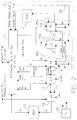
- FIG. 4 is a simplified functional block diagram of the CK chip 16.
- Signals representing AX ERRORs, FP ERRORs, DN ERRORs, CD BPU errors and DD BPU errors are ORed in an OR-gate 50. If one of these errors occurs, an indication of the presence of an error condition is latched by flipflop 51, and its Q output is applied as one input to an OR-gate 54 which therefore issues a BPU STOP signal.
- the output of the OR-gate 50 is employed as a BPU ERROR signal to advise the SP.
- CD chip detected CPU errors and DD chip detected CPU errors are ORed in an OR-gate 52, and the occurrence of one of these errors results in the output of the OR-gate 52 issuing a CPU ERROR signal to the SP and latching in the presence of an error condition into flipflop 53.
- Result compare errors ORed by OR-gate 60, are used to set a flipflop 59 whose Q output is employed as the UNDO signal and also drives an input to OR-gate 54 such that the presence of a compare error also results in the issuance of a BPU STOP signal.
- the OR-gate 54 issues the BPU STOP signal to the CK and DD chips (FIG. 3) if a BPU error occurs.
- the Q output from the flipflop 53 and the BPU STOP signal are ORed by OR-gate 61 whose output is applied to the inverting input of an AND-gate 55 which has its non-inverting input driven by the clock generator 56.
- the clock generator 56 issues a conventional stream of non-overlapping ⁇ 1 and ⁇ 2 clock pulses at a rate governed by the CMU as previously noted.
- the AND-gate 55 is disabled, and the BPU CLOCK is interrupted instituting a BPU freeze.
- the Q output from the flipflop 53 coupled to the inverting input of an AND-gate 57, interrupts the clock stream to the non-BPU logic of the CPU, such that, in concert with the AND-gate 55, the AND-gate 57 institutes a CPU freeze condition.
- the DD chip determines that the BPU should be temporarily unfrozen, it issues the UNFREEZE signal (FIG. 3) which is ORed with the RESUME signal from the SP. Thus, either signal will reset the flipflops 51, 52, 53 which may have been set by the various error signals to reenable the AND-gates 55 and (if disabled) 57 to restart operation. If appropriate, the DD chip can again invoke a BPU or CPU freeze after the conditions it seeks are established.
- FIG. 6 is a simplified representation of the timing between successive instructions executed in an exemplary four stage pipelined processor.
- instruction I4 fails in its fetch phase (during clock cycle t3), it might be advantageous to go ahead and perform the operations normally occurring during t4 and t5 to permit instructions I2 and I3 to complete execution before the AX chip issues an error signal to the CK chip.
- the faulting instruction to execute and the transfer of the contents of the software visible registers to be transferred to XRAM before freezing the BPU such that the safestore information may contain more information useful to the SP and/or operating system for diagnosing the source of the error and the remedial course to be attempted.
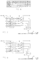
- FIG. 7 is a simplified representation of the relevant logic assuming an exemplary four stage pipeline requiring one clock cycle per stage.
- An error may occur at any stage of the operation stack 39 (containing stages 40, 41, 42, 43) to cause the issuance of a local error signal. If an error should occur during the execution stage, the error signal is applied directly to an OR-gate 48. However, if an error occurs at an earlier stage in the pipeline, the local error signal is applied to the input of one of three delay blocks 44, 45, 46 which delay the issuance of an error signal to the OR-gate 48 by three, two and one cycles, respectively.
- OR-gate 48 is OR-ed with other AX chip errors by the OR-gate 49 whose output is coupled to one input of OR-gate 33 as shown in FIG. 3.
- FIG. 8 shows a variant configuration in which a failing instruction is allowed to complete execution.
- delay block 47 is interposed intermediate the execute block and the OR-gate 48, and the respective cycle delays in the delay blocks 44, 45, 46, 47 are 4, 3, 2, and 1.
- the AX unit is microprogrammed VLSI, either the FIG. 7 and FIG. 8 configuration can be realized dynamically under appropriate conditions.
Abstract
Description
- This invention relates to information processing systems and, more particularly, to error handling facility in a Very Large Scale Integrated (VLSI) circuit Central Processing Unit (CPU) employing a pipelined address and execution module.
- In the design of a mainframe CPU employing VLSI technology, it is desirable to limit the number of different types of VLSI chips employed in order to contain the design task within manageable bounds. However, it is also highly desirable to provide powerful and reliable error detection and handling features, and this requirement has mandated the provision of various circuits, firmware and software to sense and resolve the diverse types of errors which may occur in operation.
- One VLSI chip or logic group in a CPU according to the present invention is an address and execution (AX) unit, a microprocessing engine which performs all address preparation and executes all instructions except decimal arithmetic, binary floating point and multiply/divide instructions. Such AX units are typically "pipelined" such that the various stages involved in fetching, analyzing, preparing and executing several instructions are all in process simultaneously. If all or most CPU errors from the various VLSI units, including the AX unit, are reported to a central error handling facility immediately upon occurrence for the institution of a partial or complete CPU "freeze", it is possible that instructions executing correctly in the pipeline will be aborted because of an AX error detected in the processing of an instruction in an earlier pipeline stage. As a result, performance will be adversely affected, particularly if a restart is undertaken since the instructions earlier in the pipeline than the faulting instruction will have to be reprocessed. Further, in some instances, there would be value in allowing the faulting instruction to execute before a partial or complete CPU freeze is implemented. It is to addressing these problems in a VLSI CPU that the present invention is directed.
- It is therefore a broad object of this invention to provide improved error handling capability in a VLSI CPU.
- It is a more specific object of this invention to provide such improved error handling capability which includes a central CPU error collection facility and means within an AX unit to delay reporting of an AX error under certain conditions.
- It is a still more specific object of this invention to provide means within the AX unit to delay reporting of an error sensed in the processing of an instruction in a pipeline until all earlier instructions in the pipeline have completed execution.
- In a variant, it is a still more specific object of this invention to provide means within the AX unit to delay reporting of an error sensed in the processing of an instruction in a pipeline until that instruction has completed execution.
- Briefly, these and other objects of the invention are achieved in a basic processing unit (BPU) including an AX unit (as well as a decimal numeric - DN - unit and a floating point - FP - unit) having a plurality of software visible registers and which issues an AX ERROR signal in response, among others, to sensed errors occurring within the AX unit during the processing and execution of instructions. An auxiliary (XRAM) memory receives and temporarily stores a record of the contents of the software visible registers concurrently with the availability of the result of each instruction executed by the AX unit, this operation preferably taking place via a cache memory unit. A clock unit is coupled to receive the AX ERROR signal and responds by suspending clock signals to the BPU as well as notifying a service processor (SP) of the error occurrence. The relevant contents of the XRAM are also forwarded to the SP for analysis, and the SP can order a restart by issuing a RESUME signal to the clock unit after the information obtained from the XRAM has been analyzed and the failing CPU reinitialized as necessary.
- Preferably, assuming that the AX unit is pipelined and that the error has occurred during the preparation and execution activity associated with the pipeline, the issuance of an AX ERROR signal is delayed until all instructions in the pipe ahead of the faulting instruction have completed execution. Alternatively, the delay can be extended until all instructions in the pipe ahead of and including the faulting instruction have completed execution.
- The subject matter of the invention is particularly pointed out and distinctly claimed in the concluding portion of the specification. The invention, however, both as to organization and method of operation, may best be understood by reference to the following description taken in conjunction with the subjoined claims and the accompanying drawing of which:
- FIG. 1 is a very high level block diagram of the central system structure of an information processing system in which the subject invention finds application;
- FIG. 2 is a general block diagram of the central processing unit of the central system structure of FIG. 1, in which central processing unit the subject invention is employed;
- FIG. 3 is a special purpose block diagram of the central processing unit revealing the error detection and handling aspects of the relationships among the several logic elements;
- FIG. 4 is a data flow block diagram of the clock chip which is an important element in the detection and handling of errors within the central processing unit;
- FIG. 5 is a high level block diagram illustrating the manner in which certain vital information is transferred during the error handling process to a service processor;
- FIG. 6 is a representation of an exemplary pipeline;
- FIG. 7 is a block diagram of logic within an AX unit for delaying the issuance of an AX ERROR signal under certain conditions; and
- FIG. 8 is a block diagram of variant logic within an AX unit for obtaining a slightly different result than the logic of FIG. 7.
- Attention is first directed to FIG. 1 which illustrates an exemplary Central Subsystem Structure (CSS) within which the subject invention may be incorporated. The System Control Unit (SCU) 1 centralizes and controls the
system bus 2 and thememory bus 3 scheduling. More particularly, the SCU 1: A) performs memory control, single bit error correction and double bit error detection; B) controls the memory configuration of which there are one per Memory Unit (MU) 4; C) manages 64-byte block transfers between the Central Processing Units (CPUs) 5 and the MUs in conjunction with the store-into-cache feature of the CPUs; D) corrects single bit errors found in modified blocks of a CPU's cache or on a data transfer from a CPU, MU or Input/Output Unit (IOU) 6; and E) contains the system calender clock. - The
system bus 2 interconnects 1 to 4 CPUs and 1 to 4 IOUs with each other and with the SCU. The system bus includes a 16-byte bidirectional data interface, a bidirectional address and command interface, an SCU status interface monitored by all CPUs and IOUs, and a small number of control lines between the SCU and each individual CPU and IOU. Data is exchanged on the system bus in 16, 32 or 64-byte groups, and data exchanges can be between a CPU and an MU, an IOU and an MU, two CPUs and a CPU and an IOU. The operations through thesystem bus 2 are: - Read: 16, 32 or 64 bytes;
- Read with exclusivity: 64 bytes;
- Write from IOU: 16, 32 or 64 bytes;
- Write from CPU (swapping): 64 bytes;
- Interrupts and Connects;- Read/Write registers.
- Every system bus operation consists of an address phase and a data phase, and an address phase can start every two machine cycles. Consecutive 16-byte data transfers within a group can occur on consecutive machine cycles. An IOU or CPU can wait for the data phase of up to two requests at the same time. The data blocks are transferred in the same order as the requests are received.
- The
memory bus 3 interconnects 1 to 8 MUs with the SCU. The memory bus includes a 16-byte bidirectional data interface, an address and command interface from the SCU to all MUs and a small number of control lines between the SCU and each individual MU. Data is exchanged on the memory bus in 16, 32 or 64-byte groups. The operations through thememory bus 3 are: - Read: 16, 32 or 64 bytes;
- Write: 16, 32 or 64 bytes.
- The main memory is composed of up to eight MUs. (A ninth slot, MU 4A, may be provided for ease of reconfiguration and repair in case of failure.) A single bit correction, double bit detection code is stored with every double word; i.e., 8 code bits for every 72 data bits. The code is arranged so that a 4-bit error within a single chip is corrected as four single bit errors in four different words. Data in an MU is addressed from the SCU in 16 byte (four word) increments. All bytes within any one MU are consecutively addressed; i.e., there is no interlace between MUs which operate in parallel. A memory cycle may start every machine cycle, and a memory cycle, as seen from a CPU, is ten machine cycles, assuming no conflicts with other units. An
MU 4 contains 160 Dynamic Random Access Memory (DRAM) circuits, each of which has n by 4 bit storage elements where n = 256, 1024 or 4096. - The IOUs 6 each provide a connection between the
system bus 2 and two Input/Output Buses (IOBs) 7 such that each IOB interfaces with a single IOU. Thus, an IOU manages data transfers between the CSS and the I/O subsystems, not shown in FIG. 1. - A Clock and Maintenance Unit (CMU) 8 generates, distributes and tunes the clock signals for all the units in the CSS, provides the interface between the service processor(s) (SP) 9 and the central processing, input/output and power subsystems, initializes the units of the CSS and processes errors detected within the CSS units. The CSS employs a two-phase clock system and latched register elements in which the trailing edge of
clock 1 defines the end ofphase 1, and the trailing edge ofclock 2 defines the end of phase two, each phase thus being one-half of a machine cycle. - The SP(s) 9 may be a commodity personal computer with an integrated modem for facilitating remote maintenance and operations, and large systems may include two SPs through which the system can be dynamically reconfigured for high availability. The SP performs four major functions:
- monitors and controls the CSS during initialization, error logging or diagnostic operations;
- serves as the primary operating system console during system boot or on operator command;
- serves as console and data server for the input/output subsystems Maintenance Channel Adaptor (MCA);
- provides a remote maintenance interface.
- Attention is now directed to FIG. 2 which is a general block diagram of one of the CPUs 5 of FIG. 1. The Address and Execution Unit (AX unit) is a microprocessing engine which performs all address preparation and executes all instructions except decimal arithmetic, binary floating point and multiply/divide instructions. Two identical AX chips 10, 10A perform duplicate actions in parallel, and the resulting AX chip outputs are constantly compared to detect errors. The structure of the AX chip will be described in more detail below. The main functions performed by the AX unit include:
- effective and virtual address formation;
- memory access control;
- security checks;
- register change/use control;
- execution or basic instructions, shift instructions, security instructions, character manipulation and miscellaneous instructions.
- The cache unit includes a data part of 64K bytes (16K words) and a set associative directory part which defines the main memory location of each 64-byte (16-word) block stored in the cache data part. Physically, the cache unit is implemented in an array of ten
DT chips 11, a cache directory (CD)chip 12 and a duplicate directory (DD)chip 13. Each of the DT, CD and DD chips will be described in more detail below. - The specific functions performed by the
DT chip array 11 include: - combined instruction and operand data storage;
- instruction and operand buffering and alignment;
- data interface with the system bus 7 (FIG. 1);
- CLIMB safestore file.
- The cache write strategy is "store into". If a longitudinal parity error is detected when reading a portion of a modified block from the cache, the block will be swapped out of the cache, corrected by the SCU and written into main memory. The corrected block will then be refetched from main memory.
- Two copies of the cache directory information are respectively maintained in the CD and DD chips which perform different logic functions. The two directory copies allow interrogation of the cache contents from the system bus in parallel and without interference with instruction/operand access from the CPUs and also provide for error recovery.
Functions performed by theCD chip 12 include: - cache directory for CPU accesses;
- instruction, operand and store buffer management;
- virtual-to-real address translation paging buffer.
- cache directory for system accesses;
- system bus control;
- distributed connect/interrupt management;
- cache directory error recovery.
- Efficient scientific calculation capability is implemented on the Floating Point (FP) chips 15, 15A. The identical FP chips execute all binary floating point arithmetic in duplicate. These chips, operating in concert with the duplicate AX chips 10, 10A, perform scalar or vector scientific processing.
- The FP chip 15 (duplicated by the
FP chip 15A): - executes all binary and fixed and floating point multiply and divide operations;
- computes 12 by 72-bit partial products in one machine cycle;
- computes eight quotient bits per divide cycle;
- performs modulo 15 residue integrity checks.
- Functions performed by the FP chips 15, 15A include:
- executes all floating point mantissa arithmetic except multiply and divide;
- executes all exponent operations in either binary or hexadecimal format;
- preprocesses operands and postprocesses results for multiply and divide instructions;
- provides indicator and status control.
- Two special purpose random access memories (
FRAM 17 and XRAM 18) are incorporated into the CPU. TheFRAM chip 17 is an adjunct to the FP chips 15, 15A and functions as an FP control store and decimal integer table lookup. TheXRAM chip 18 is an adjunct to the AX chips 10 10A and serves as a scratchpad as well as providing safestore and patch functions. - The CPU also employs a Clock Distribution (CK)
chip 16 whose functions include: - clock distribution to the several chips constituting the CPU;
- shift path control;
- maintenance;
- interface between CMU and CPU;
- provision of clock stop logic for error detection and recovery.
- The DN chip 14 (in parallel with the
DN chip 14A) performs the execution of the decimal numeric Extended Instruction Set (EIS) instructions. It also executes the Decimal-to-Binary (DTB), Binary-to-Decimal (BTD) conversion EIS instructions and Move-Numeric-Edit (MVNE) EIS instructions in conjunction with theAX chip 10. The DN chip both receives operands from memory and sends results to memory via thecache unit 11. - The AX, DN and FP chips, collectively, are sometimes referred to as the Basic Processing Unit (BPU). It was previously noted that the AX, DN and FP chips were duplicated with the duplicate units operating in parallel to obtain duplicate results which are available for integrity checking. (The unit pairs are respectively named the AX unit, the DN unit and the FP unit for convenience.) Thus, master and slave results are obtained in the normal operation of these chips. The master results are placed onto a Master Result Bus (MRB) 20 while the slave results are placed onto a Slave Result Bus (SRB) 21. Both the master and slave results are conveyed, on the MRB and SRB respectively, to the
cache data array 11 of DT chips. The purposes of this arrangement will be described more fully below. In addition, aCOMTO bus 22 and aCOMFROM bus 23 couple together the AX unit, the DN unit and the FP unit for certain interrelated operations as will also be described more fully below. - Those skilled in the art will understand that a VLSI CPU is subject to the occurrence of numerous errors. While state of the art VLSI CPU's are very reliable and may run for long periods with no errors whatever occurring, there is little tolerance in many applications for accommodating even occasional errors. As a result, it is necessary to provide many error sensing and recovery circuits throughout the logic of a CPU to detect several types of errors such as parity errors (as a common example) which may occur when information is transferred between elements of the CPU. As previously noted, in the specific CPU chosen for illustration and in which the invention finds particular application, the outputs of duplicate master and slave AX, FP and DN chips are compared for identical results, and the content of the Master and Slave Result Busses are compared in the Cache Unit for similar identity. Various other errors are sensed throughout the CPU. According to the subject invention, the CK chip has a primary role in coordinating the error handling processes in the exemplary CPU.
- Attention is now directed to FIG. 3 in which the CPU is shown in a redrawn configuration more specifically oriented to disclose the present invention which is directed to certain aspects of the system facility for handling sensed CPU errors. It will be seen that numerous errors are reported to the
CK chip 16. The CPU has a variety of sources of internally detected errors which are classified as hardware retryable, software retryable or non-retryable. Hardware retryable errors are those which are directly compensated by the hardware without involvement or intervention by the software operating system and with little or no involvement by the SP 9 (FIG. 1) to which all errors are reported. Certain paging and cache directory errors, for example, are deemed hardware retryable. For other error conditions, which may be software retryable or non-retryable, theCK chip 16 will either cause a freeze of BPU or CPU clocks as quickly as possible to minimize any loss of data relating to the failing condition or it will invoke a suspension of BPU and system bus operation. Two types of software retry are employed, one corresponding to a freeze and the other to a suspend. If a clock freeze occurs, the machine state is extracted by the SP and provided to the operating system for retry. If a BPU or CPU suspension occurs, the SP may direct a CPU resume, and the operating system will attempt a software retry. - All errors are reported to the SP which scans safestore information and other information to make a preliminary determination regarding the ability of the error-detecting CPU (or another CPU) to attempt a retry. Retry conditions are further evaluated by the operating system, and the actual software retry is done by execution on one of the CPUs.
- Referring briefly to FIG. 5, a simplified logic diagram is given illustrating the manner in which the safestore information may be communicated to the SP under error conditions. Whenever the AX chip 10 (10A) places a result on the result bus 20 (21), the contents of the software
visible registers 34 are simultaneously transferred to areserved safestore buffer 35 in theXRAM 18 via temporary storage in thecache unit 11. If an error signal is sent to theCK chip 16 by one of the several VLSI chips of the CPU, theDD chip 13 is notified (as will be discussed further below). The DD chip provides an address and a write enable to the XRAM to extract the then resident safestore frame for transfer (as represented by the AND-gate array 36) to the SP for analysis via thecache unit 11. - Referring again to FIG. 3, some of the major error types and sources will be briefly described. Each of the AX chips 10, 10A, FP chips 15, 15A and DN chips 14, 14A combine multiple error signal lines (as represented by OR-
gates CK chip 16. The majority of the checked logic areas sense parity errors during data transfers, but other error types, such as directory read mismatch, DIR Level In/Out miscompares, illegal command sequence, increment miscount, multiple directory hit, etc. as well as several types of compares are all monitored. TheCD chip 12 andDD chip 13 each send separate BPU error and CPU error signals to the CK chip. - As has been mentioned briefly above, the
master result bus 20 and theslave result bus 21 are checked for identity in thecache unit 11 by the compare logic in that logic block. The manner in which the result bus compare is performed is treated in detail in copending U.S. patent application Serial No. 07/546,204, entitled EFFICIENT ERROR DETECTION IN A VLSI CENTRAL PROCESSING UNIT by Russell W. Guenthner et al which is assigned to the Assignee of the present invention. Briefly, corresponding bit positions on the result busses are applied to first and second inputs of one gate of an Exclusive OR-gate (or Exclusive NOR-gate) array in which the outputs are common such that any mismatch at any bit position is reflected as an error signal, appearing at the common output, which is coupled to theCK chip 16. Similar compare logic circuitry may be employed in theblocks - AX errors, FP errors, DN errors and result bus errors are all deemed to be BPU errors. However, the
CD chip 12 and theDD chip 13 can detect and advise theCK chip 16 of either BPU errors or CPU errors (for example, cache errors) which are treated differently. In addition, the CD and DD chips are notified of BPU errors originating elsewhere, and, under certain conditions (such as during a hardware/firmware troubleshooting process), theDD chip 13 may order a temporary "unfreeze" of the BPU clock. Certain cache errors are reported directly to theDD chip 13 which then determines if a BPU or CPU error signal is to be forwarded to theCK chip 16. - Attention is now directed to FIG. 4 which is a simplified functional block diagram of the
CK chip 16. Signals representing AX ERRORs, FP ERRORs, DN ERRORs, CD BPU errors and DD BPU errors are ORed in an OR-gate 50. If one of these errors occurs, an indication of the presence of an error condition is latched byflipflop 51, and its Q output is applied as one input to an OR-gate 54 which therefore issues a BPU STOP signal In addition, the output of the OR-gate 50 is employed as a BPU ERROR signal to advise the SP. Similarly, CD chip detected CPU errors and DD chip detected CPU errors are ORed in an OR-gate 52, and the occurrence of one of these errors results in the output of the OR-gate 52 issuing a CPU ERROR signal to the SP and latching in the presence of an error condition intoflipflop 53. Result compare errors, ORed byOR-gate 60, are used to set aflipflop 59 whose Q output is employed as the UNDO signal and also drives an input to OR-gate 54 such that the presence of a compare error also results in the issuance of a BPU STOP signal. - Thus, the OR-gate 54 issues the BPU STOP signal to the CK and DD chips (FIG. 3) if a BPU error occurs. The Q output from the
flipflop 53 and the BPU STOP signal are ORed byOR-gate 61 whose output is applied to the inverting input of an AND-gate 55 which has its non-inverting input driven by theclock generator 56. Theclock generator 56 issues a conventional stream of non-overlapping Φ1 and Φ2 clock pulses at a rate governed by the CMU as previously noted. Thus, if either a BPU error or a CPU error occurs, the AND-gate 55 is disabled, and the BPU CLOCK is interrupted instituting a BPU freeze. Similarly, if a CPU error occurs, the Q output from theflipflop 53, coupled to the inverting input of an AND-gate 57, interrupts the clock stream to the non-BPU logic of the CPU, such that, in concert with the AND-gate 55, the AND-gate 57 institutes a CPU freeze condition. - If a BPU STOP signal has issued and the DD chip determines that the BPU should be temporarily unfrozen, it issues the UNFREEZE signal (FIG. 3) which is ORed with the RESUME signal from the SP. Thus, either signal will reset the
flipflops gates 55 and (if disabled) 57 to restart operation. If appropriate, the DD chip can again invoke a BPU or CPU freeze after the conditions it seeks are established. - As previously discussed, it may not be desirable to immediately freeze the AX chip 10 (10A) if a fault arises in the development and execution of an instruction which is later in a pipeline than one or more non-faulting instructions. This concept may be more readily appreciated by reference to FIG. 6 which is a simplified representation of the timing between successive instructions executed in an exemplary four stage pipelined processor. Thus, if, for example, instruction I4 fails in its fetch phase (during clock cycle t3), it might be advantageous to go ahead and perform the operations normally occurring during t4 and t5 to permit instructions I2 and I3 to complete execution before the AX chip issues an error signal to the CK chip. In some CPUs and/or under some conditions, it may be advantageous to permit the faulting instruction to execute and the transfer of the contents of the software visible registers to be transferred to XRAM before freezing the BPU such that the safestore information may contain more information useful to the SP and/or operating system for diagnosing the source of the error and the remedial course to be attempted.
- A process for obtaining the desired delay in forwarding errors observed in the AX chip 10 (10A) during instruction sequencing is shown in FIG. 7 which is a simplified representation of the relevant logic assuming an exemplary four stage pipeline requiring one clock cycle per stage. An error may occur at any stage of the operation stack 39 (containing
stages - FIG. 8 shows a variant configuration in which a failing instruction is allowed to complete execution. Thus,
delay block 47 is interposed intermediate the execute block and the OR-gate 48, and the respective cycle delays in the delay blocks 44, 45, 46, 47 are 4, 3, 2, and 1. In actual practice in which the AX unit is microprogrammed VLSI, either the FIG. 7 and FIG. 8 configuration can be realized dynamically under appropriate conditions. - While the representation of structure shown in the several figures may be used to construct actual circuitry, it will be understood that both the
AX chip 10 and theCK chip 16 are, in the exemplary embodiment, actually implemented in microprogrammed and/or hardwired VLSI technology. Those skilled in the art will appreciate that pictorial and logical representations of VLSI circuitry are very difficult to comprehend unless the peruser is intimately familiar with the actual VLSI circuitry under study and, if used, its microprogramming; hence the necessity for the use of conceptual, functionally equivalent, logic diagrams to set forth the invention. Further, those skilled in the art will also appreciate that, as the limits of integration are pushed, an entire CPU employing the features of the present invention may be soon realized on a single chip, and the fact that the described embodiment is implemented among several VLSI chips is not intended to be a limitation on the invention. - Thus, while the principles of the invention have now been made clear in an illustrative embodiment, there will be immediately obvious to those skilled in the art many modifications of structure, arrangements, proportions, the elements, materials, and components, used in the practice of the invention which are particularly adapted for specific environments and operating requirements without departing from those principles.
Claims (6)
- A central processing unit incorporated into a data processing system including a service processor and an error handling facility, which central processing unit includes:A) a basic processing unit including an address and execution unit having:1) a plurality of software visible registers; and2) means for issuing an AX ERROR signal in response to sensed errors occurring within said address and execution unit during the processing and execution of instructions;B) an auxiliary memory adapted to receive and temporarily store a record of the contents of said software visible registers concurrently with the availability of the result of each instruction executed by said address and execution unit;C) a clock unit coupled to receive said AX ERROR signal and adapted to suspend clock signals to said basic processing unit in response thereto;D) means responsive to the suspension of clock signals to said basic processing unit to transfer said record of the contents of said software visible registers from said auxiliary memory to said service processor for analysis; andE) means within said clock unit to restart clock signals to said basic processing unit in response to the receipt of a resume signal from said service processor.
- The central processing unit of Claim 1 in which said address and execution unit incorporates a pipelined processor and which further includes means for delaying the issuance of an AX ERROR signal until all instructions in the pipe ahead of the faulting instruction have completed execution.
- The central processing unit of Claim 1 in which said address and execution unit incorporates a pipelined processor and which further includes means for delaying the issuance of an AX ERROR signal until all instructions in the pipe ahead of and including the faulting instruction have completed execution.
- The central processing unit of Claim 1 which further includes a cache memory and in which said record of said software visible registers are transferred to said auxiliary memory from said address and execution unit and from said auxiliary memory to said service processor via said cache memory.
- The central processing unit of Claim 2 which further includes a cache memory and in which said record Of said software visible registers are transferred to said auxiliary memory from said address and execution unit and from said auxiliary memory to said service processor via said cache memory.
- The central processing unit of Claim 3 which further includes a cache memory and in which said record of said software visible registers are transferred to said auxiliary memory from said address and execution unit and from said auxiliary memory to said service processor via said cache memory.
Applications Claiming Priority (2)
| Application Number | Priority Date | Filing Date | Title |
|---|---|---|---|
| US584229 | 1984-02-27 | ||
| US58422990A | 1990-09-18 | 1990-09-18 |
Publications (3)
| Publication Number | Publication Date |
|---|---|
| EP0476262A2 true EP0476262A2 (en) | 1992-03-25 |
| EP0476262A3 EP0476262A3 (en) | 1993-05-19 |
| EP0476262B1 EP0476262B1 (en) | 1997-06-18 |
Family
ID=24336459
Family Applications (1)
| Application Number | Title | Priority Date | Filing Date |
|---|---|---|---|
| EP19910112135 Expired - Lifetime EP0476262B1 (en) | 1990-09-18 | 1991-07-19 | Error handling in a VLSI central processor unit employing a pipelined address and execution module |
Country Status (3)
| Country | Link |
|---|---|
| EP (1) | EP0476262B1 (en) |
| AU (1) | AU644160B2 (en) |
| DE (1) | DE69126584T2 (en) |
Citations (2)
| Publication number | Priority date | Publication date | Assignee | Title |
|---|---|---|---|---|
| US4875160A (en) * | 1988-07-20 | 1989-10-17 | Digital Equipment Corporation | Method for implementing synchronous pipeline exception recovery |
| US4920477A (en) * | 1987-04-20 | 1990-04-24 | Multiflow Computer, Inc. | Virtual address table look aside buffer miss recovery method and apparatus |
Family Cites Families (2)
| Publication number | Priority date | Publication date | Assignee | Title |
|---|---|---|---|---|
| GB8828817D0 (en) * | 1988-12-09 | 1989-01-18 | Int Computers Ltd | Data processing apparatus |
| US4982402A (en) * | 1989-02-03 | 1991-01-01 | Digital Equipment Corporation | Method and apparatus for detecting and correcting errors in a pipelined computer system |
-
1991
- 1991-05-03 AU AU76377/91A patent/AU644160B2/en not_active Ceased
- 1991-07-19 DE DE1991626584 patent/DE69126584T2/en not_active Expired - Fee Related
- 1991-07-19 EP EP19910112135 patent/EP0476262B1/en not_active Expired - Lifetime
Patent Citations (2)
| Publication number | Priority date | Publication date | Assignee | Title |
|---|---|---|---|---|
| US4920477A (en) * | 1987-04-20 | 1990-04-24 | Multiflow Computer, Inc. | Virtual address table look aside buffer miss recovery method and apparatus |
| US4875160A (en) * | 1988-07-20 | 1989-10-17 | Digital Equipment Corporation | Method for implementing synchronous pipeline exception recovery |
Also Published As
| Publication number | Publication date |
|---|---|
| DE69126584T2 (en) | 1998-02-05 |
| AU644160B2 (en) | 1993-12-02 |
| EP0476262A3 (en) | 1993-05-19 |
| DE69126584D1 (en) | 1997-07-24 |
| AU7637791A (en) | 1992-03-26 |
| EP0476262B1 (en) | 1997-06-18 |
Similar Documents
| Publication | Publication Date | Title |
|---|---|---|
| EP0516126B1 (en) | Fault tolerant multiprocessor computer system | |
| US4751639A (en) | Virtual command rollback in a fault tolerant data processing system | |
| US5317726A (en) | Multiple-processor computer system with asynchronous execution of identical code streams | |
| US5276823A (en) | Fault-tolerant computer system with redesignation of peripheral processor | |
| US5890003A (en) | Interrupts between asynchronously operating CPUs in fault tolerant computer system | |
| US5384906A (en) | Method and apparatus for synchronizing a plurality of processors | |
| JPS6353571B2 (en) | ||
| JP2500038B2 (en) | Multiprocessor computer system, fault tolerant processing method and data processing system | |
| US5195101A (en) | Efficient error detection in a vlsi central processing unit | |
| US4805095A (en) | Circuit and a method for the selection of original data from a register log containing original and modified data | |
| US5263034A (en) | Error detection in the basic processing unit of a VLSI central processor | |
| US5251321A (en) | Binary to binary coded decimal and binary coded decimal to binary conversion in a VLSI central processing unit | |
| US5276862A (en) | Safestore frame implementation in a central processor | |
| US5553232A (en) | Automated safestore stack generation and move in a fault tolerant central processor | |
| US5557737A (en) | Automated safestore stack generation and recovery in a fault tolerant central processor | |
| EP0550283A2 (en) | Invoking hardware recovery actions via action latches | |
| US5408651A (en) | Store "undo" for cache store error recovery | |
| CN111190774B (en) | Configurable dual-mode redundancy structure of multi-core processor | |
| US5905857A (en) | Safestore procedure for efficient recovery following a fault during execution of an iterative execution instruction | |
| EP0476262B1 (en) | Error handling in a VLSI central processor unit employing a pipelined address and execution module | |
| US5422837A (en) | Apparatus for detecting differences between double precision results produced by dual processing units operating in parallel | |
| JPH0628251A (en) | Trouble-resistamt multiprocessor computer system | |
| JPH0622001B2 (en) | Memory management unit of computer system |
Legal Events
| Date | Code | Title | Description |
|---|---|---|---|
| PUAI | Public reference made under article 153(3) epc to a published international application that has entered the european phase |
Free format text: ORIGINAL CODE: 0009012 |
|
| AK | Designated contracting states |
Kind code of ref document: A2 Designated state(s): DE FR GB IT |
|
| PUAL | Search report despatched |
Free format text: ORIGINAL CODE: 0009013 |
|
| AK | Designated contracting states |
Kind code of ref document: A3 Designated state(s): DE FR GB IT |
|
| 17P | Request for examination filed |
Effective date: 19930831 |
|
| RAP1 | Party data changed (applicant data changed or rights of an application transferred) |
Owner name: BULL HN INFORMATION SYSTEMS INC. |
|
| RAP1 | Party data changed (applicant data changed or rights of an application transferred) |
Owner name: BULL HN INFORMATION SYSTEMS INC. |
|
| 17Q | First examination report despatched |
Effective date: 19951011 |
|
| GRAG | Despatch of communication of intention to grant |
Free format text: ORIGINAL CODE: EPIDOS AGRA |
|
| GRAH | Despatch of communication of intention to grant a patent |
Free format text: ORIGINAL CODE: EPIDOS IGRA |
|
| GRAH | Despatch of communication of intention to grant a patent |
Free format text: ORIGINAL CODE: EPIDOS IGRA |
|
| GRAA | (expected) grant |
Free format text: ORIGINAL CODE: 0009210 |
|
| AK | Designated contracting states |
Kind code of ref document: B1 Designated state(s): DE FR GB IT |
|
| PG25 | Lapsed in a contracting state [announced via postgrant information from national office to epo] |
Ref country code: FR Free format text: THE PATENT HAS BEEN ANNULLED BY A DECISION OF A NATIONAL AUTHORITY Effective date: 19970618 |
|
| REF | Corresponds to: |
Ref document number: 69126584 Country of ref document: DE Date of ref document: 19970724 |
|
| PG25 | Lapsed in a contracting state [announced via postgrant information from national office to epo] |
Ref country code: GB Free format text: LAPSE BECAUSE OF NON-PAYMENT OF DUE FEES Effective date: 19970918 |
|
| ET | Fr: translation filed | ||
| PLBE | No opposition filed within time limit |
Free format text: ORIGINAL CODE: 0009261 |
|
| STAA | Information on the status of an ep patent application or granted ep patent |
Free format text: STATUS: NO OPPOSITION FILED WITHIN TIME LIMIT |
|
| GBPC | Gb: european patent ceased through non-payment of renewal fee |
Effective date: 19970918 |
|
| 26N | No opposition filed | ||
| REG | Reference to a national code |
Ref country code: FR Ref legal event code: ST |
|
| PGFP | Annual fee paid to national office [announced via postgrant information from national office to epo] |
Ref country code: DE Payment date: 20060630 Year of fee payment: 16 |
|
| PGFP | Annual fee paid to national office [announced via postgrant information from national office to epo] |
Ref country code: IT Payment date: 20070726 Year of fee payment: 17 |
|
| PG25 | Lapsed in a contracting state [announced via postgrant information from national office to epo] |
Ref country code: DE Free format text: LAPSE BECAUSE OF NON-PAYMENT OF DUE FEES Effective date: 20080201 |
|
| PG25 | Lapsed in a contracting state [announced via postgrant information from national office to epo] |
Ref country code: IT Free format text: LAPSE BECAUSE OF NON-PAYMENT OF DUE FEES Effective date: 20080719 |