EP0473384B1 - Coding apparatus for digital image signals - Google Patents
Coding apparatus for digital image signals Download PDFInfo
- Publication number
- EP0473384B1 EP0473384B1 EP19910307804 EP91307804A EP0473384B1 EP 0473384 B1 EP0473384 B1 EP 0473384B1 EP 19910307804 EP19910307804 EP 19910307804 EP 91307804 A EP91307804 A EP 91307804A EP 0473384 B1 EP0473384 B1 EP 0473384B1
- Authority
- EP
- European Patent Office
- Prior art keywords
- circuit
- block
- frame
- output signal
- data
- Prior art date
- Legal status (The legal status is an assumption and is not a legal conclusion. Google has not performed a legal analysis and makes no representation as to the accuracy of the status listed.)
- Expired - Lifetime
Links
Images


Classifications
-
- H—ELECTRICITY
- H04—ELECTRIC COMMUNICATION TECHNIQUE
- H04N—PICTORIAL COMMUNICATION, e.g. TELEVISION
- H04N19/00—Methods or arrangements for coding, decoding, compressing or decompressing digital video signals
- H04N19/90—Methods or arrangements for coding, decoding, compressing or decompressing digital video signals using coding techniques not provided for in groups H04N19/10-H04N19/85, e.g. fractals
- H04N19/98—Adaptive-dynamic-range coding [ADRC]
-
- H—ELECTRICITY
- H04—ELECTRIC COMMUNICATION TECHNIQUE
- H04N—PICTORIAL COMMUNICATION, e.g. TELEVISION
- H04N19/00—Methods or arrangements for coding, decoding, compressing or decompressing digital video signals
- H04N19/10—Methods or arrangements for coding, decoding, compressing or decompressing digital video signals using adaptive coding
- H04N19/102—Methods or arrangements for coding, decoding, compressing or decompressing digital video signals using adaptive coding characterised by the element, parameter or selection affected or controlled by the adaptive coding
- H04N19/132—Sampling, masking or truncation of coding units, e.g. adaptive resampling, frame skipping, frame interpolation or high-frequency transform coefficient masking
-
- H—ELECTRICITY
- H04—ELECTRIC COMMUNICATION TECHNIQUE
- H04N—PICTORIAL COMMUNICATION, e.g. TELEVISION
- H04N19/00—Methods or arrangements for coding, decoding, compressing or decompressing digital video signals
- H04N19/10—Methods or arrangements for coding, decoding, compressing or decompressing digital video signals using adaptive coding
- H04N19/134—Methods or arrangements for coding, decoding, compressing or decompressing digital video signals using adaptive coding characterised by the element, parameter or criterion affecting or controlling the adaptive coding
- H04N19/146—Data rate or code amount at the encoder output
- H04N19/152—Data rate or code amount at the encoder output by measuring the fullness of the transmission buffer
-
- H—ELECTRICITY
- H04—ELECTRIC COMMUNICATION TECHNIQUE
- H04N—PICTORIAL COMMUNICATION, e.g. TELEVISION
- H04N19/00—Methods or arrangements for coding, decoding, compressing or decompressing digital video signals
- H04N19/50—Methods or arrangements for coding, decoding, compressing or decompressing digital video signals using predictive coding
- H04N19/587—Methods or arrangements for coding, decoding, compressing or decompressing digital video signals using predictive coding involving temporal sub-sampling or interpolation, e.g. decimation or subsequent interpolation of pictures in a video sequence
-
- H—ELECTRICITY
- H04—ELECTRIC COMMUNICATION TECHNIQUE
- H04N—PICTORIAL COMMUNICATION, e.g. TELEVISION
- H04N19/00—Methods or arrangements for coding, decoding, compressing or decompressing digital video signals
- H04N19/90—Methods or arrangements for coding, decoding, compressing or decompressing digital video signals using coding techniques not provided for in groups H04N19/10-H04N19/85, e.g. fractals
- H04N19/96—Tree coding, e.g. quad-tree coding
-
- H—ELECTRICITY
- H04—ELECTRIC COMMUNICATION TECHNIQUE
- H04N—PICTORIAL COMMUNICATION, e.g. TELEVISION
- H04N19/00—Methods or arrangements for coding, decoding, compressing or decompressing digital video signals
- H04N19/50—Methods or arrangements for coding, decoding, compressing or decompressing digital video signals using predictive coding
Definitions
- This invention relates to coding apparatus for digital image signals which apparatus can, for example, be used in a digital video tape recorder (VTR).
- VTR digital video tape recorder
- the minimum level (minimum value) in the block is eliminated from the input pixel data.
- the pixel data after elimination of the minimum value are converted into a representative level.
- the quantization includes dividing the dynamic range DR which has been detected into four level ranges corresponding to a bit length such as two bits smaller than the original quantization bit length, for detecting the level range to which each pixel datum in the block belongs, and for generating a code signal indicative of the level range.
- a coding apparatus in which a three-dimensional ADRC and a frame dropping process are combined in order to raise the compression ratio further.
- motion between two areas forming a three-dimensional block is detected, three-dimensional ADRC is executed in a block having motion, and in a stationary block, the transmission of one of the areas is omitted and two-dimensional ADRC is executed with respect to a block comprising a mean value of two areas.
- memory capacity of two frame is needed for a block segmentation process to form a three-dimensional block.
- a memory of two frames is further necessary to delay input data until the number of bits to be assigned has been decided by the buffering process.
- a memory capacity of two frames is also needed for a block desegmentation of a decoding apparatus. The total memory capacity required is therefore large.
- European Patent Application No. 87116594.0 discloses a system of coding moving image signals for producing a predictive error signal by a predictive coding based on inter-frame correlation and quantizing by a quantization unit, the produced predictive error signal for each block of a picture frame constituted by N lines of M pixels.
- the system includes a block coding/non-coding decision unit for calculating a first evaluation value of the predictive error signal for each block of the picture frame and deciding that a block non-coding is applicable when the first evaluation value is less than a first threshold value, and deciding that a block coding is applicable when the first evaluation value is greater than the first threshold value, the predictive error signal not being transmitted when the result of the decision is for a block non-coding, and the predictive error signal being quantized and transmitted when the result of the decision is for a block coding.
- European Patent Application No. 89301739.2 discloses an image encoding apparatus that has a memory for storing image data corresponding to an object for every frame, and a face region detecting circuit for detecting a difference between input frame image data and preceding frame image data, and extracting image data of a face region of the object on the basis of the difference data. More bits are allocated to the extracted face region than those to the remaining image region.
- a coding apparatus for a digital image signal comprising: a block segmentor for converting an input digital image signal into a first output signal having a two-dimensional block structure; a circuit for receiving and processing a second output signal, such that between a first and a second block which are located at spatially the same position and respectively belong to a pair of sequential frames of said second output signal, said first and second blocks are transmitted or not transmitted in dependence upon a control signal; a control circuit for generating said control signal; and an encoder to which pixel data of said first block and pixel data of said second block that are to be transmitted are supplied, said encoder compression encoding said pixel data on a block unit basis; said apparatus being characterised in that: said control signal is dependent upon an absolute value of a difference between values of pixel data at the same position between said first and second blocks; said control signal controls said circuit to always transmit said first block and to either transmit or not transmit said second block; and in that there is provided:
- a method of encoding a digital signal comprising: (a) converting an input digital signal into a first output signal having a two-dimensional block structure; (b) grouping sequential frames of said first output signal together in pairs; (c) sub-sampling said first output signal with a sub-sampling phase that is inverted every sequential pair of frames to produce a second output signal; (d) generating a control signal that is dependent upon an absolute value of a difference between values of pixel data at the same position between first and second blocks of sequential pair of frames of said second output signal; (e) processing said second output signal in a circuit (5), such that said first and second blocks are transmitted or not transmitted in dependence upon said control signal, said control signal instructing said circuit (5) to always transmit said first block and selectively transmit or not transmit said second block; and (f) compression encoding pixel data of said first block and pixel data of said second block that are to be transmitted on a block unit basis.
- a digital video signal is supplied via an input terminal 1 to a block segmentation circuit 2 which converts the video signal from a raster scan into a block signal. That is, a picture plane of one frame is segmented into two-dimensional blocks of, for example, (4 lines x 8 pixels). Unlike three-dimensional blocks, when two-dimensional blocks are formed, the memory capacity of the block segmentation circuit 2 can be reduced.
- An output signal from the block segmentation circuit 2 is supplied to a sub-sampling circuit 3 which halves the number of pixels by a quincunx sub-sampling pattern. Therefore, the number of pixels in one block becomes sixteen.
- a control signal to cause sub-sampling patterns of complementary forms every two frames is supplied from a terminal 4 to the sub-sampling circuit 3. Motion between the blocks can be detected from a difference of the pixel data of one frame by the sub-sampling.
- Figure 2 shows sub-sampling patterns.
- B1, B2, B3, ... denote blocks which are located spatially at the same position and respectively belong to sequential frames F1, F2, F3, ...
- a number of blocks other than the blocks shown in the diagram are included in each frame.
- ⁇ and ⁇ denote transmission pixels
- X indicates non-transmission pixels.
- the sub-sampling patterns are the same. As shown by partitioning by broken lines, the pattern of two frames and the pattern of the next two frames have complementary shapes.
- An output signal of the sub-sampling circuit 3 is supplied to a frame dropping circuit 5 to drop frames on a block unit basis, a comparing circuit 6, and a frame delay circuit 7.
- a control signal to control whether frames should be dropped or not, that is, to control the transmission/non-transmission of the block is supplied to the frame dropping circuit 5 through a switching circuit 8.
- the switching circuit 8 is controlled by a switching signal from a terminal 9 so as alternately to select input terminals a and b at one frame period.
- a signal of "1" is always supplied to the input terminal a of the switching circuit 8.
- "1" denotes that the block is transmitted. Therefore, the blocks B1, B3, B5, ... included in the first frames F1, F3, F5, ... of two sequential frames are always transmitted.
- the input terminal b of the switching circuit 8 is selected and the transmission/non- transmission is adaptively controlled. That is, the transmission/non-transmission of the block are controlled on the basis of the absolute value of a frame difference between the preceding frame and the present frame.
- the comparing circuit 6 detects a frame difference between the values of the pixels of the present frame and the preceding frame.
- the frame difference is converted into the absolute value by an absolute value forming circuit 10, an output signal of which is supplied to a summing circuit 11.
- the absolute value of the frame differences with respect to every two pixels are summed by the summing circuit 11 for one block.
- An output of the summing circuit 11 is supplied to a comparing circuit 12.
- a threshold value M regarding the motion is supplied to the comparing circuit 12 from a buffering circuit 19, which will be explained below.
- an output of the comparing circuit 12 is set to "0".
- the output of the comparing circuit 12 is set to "1".
- the frame dropping process in which the block is not terminated is executed.
- Data corresponding to the motion between the blocks can be derived by other methods.
- the output of the comparing circuit 12 to control the transmission/non-transmission of the block is also supplied to a detecting circuit 20 to detect a transmission ratio w for one frame period. Since the adaptive frame dropping is executed in the frames F2, F4, ... after every two frames, the transmission ratio w relative to the original data changes in each following frame. Since the total number of blocks in one frame is known, the ratio of the number of blocks which are transmitted to the total number is detected as the transmission ratio w.
- An output signal of the detecting circuit 20 is supplied to the buffering circuit 19. The output signal of the detecting circuit 20 is also necessary to discriminate the block which has been frame-dropped on the reception side, and is supplied as a frame dropping flag to a frame segmentation circuit 22 and is transmitted together with encoding data, which will be explained below.
- An encoder of the ADRC is connected to the frame dropping circuit 5.
- the buffering circuit 19 is provided in conjunction with the encoder.
- An output signal of the frame dropping circuit 5 is supplied to a detecting circuit 13 and a delay circuit 14.
- the detecting circuit 13 detects the dynamic range DR and the minimum value MIN of the block.
- the delay circuit 14 delays data by a time to detect the minimum value MIN and the dynamic range DR.
- a subtracting circuit 15 subtracts the minimum value MIN from the video data from the delay circuit 14, so that the video data from which the minimum value has been eliminated is derived from the subtracting circuit 15.
- the output data of the subtracting circuit 15 and the dynamic range DR are supplied to a quantizing circuit 18 through delay circuits 16 and 17, respectively.
- the quantizing circuit 18 executes a quantization adapted to the dynamic range DR. That is, the video data from which the minimum value has been eliminated are divided by a quantization step ⁇ which is obtained by dividing the dynamic range DR into 2 n equal steps. An integral value which is obtained by omitting a fraction of the quotient is used as a code signal DT.
- the quantizing circuit 18 can be constructed by a dividing circuit or a ROM.
- a bit length n which is assigned to the code signal DT is determined in a manner such that a generation data amount per predetermined period, for instance, every two frames does not exceed a target value L (bits).
- the buffering circuit 19 to which the dynamic range DR is supplied is provided.
- a plurality of, for example, 32 sets (T1, T2, T3, T4, M) of threshold values are prepared for the buffering circuit 19 as will be explained below.
- the generation data amount is set so as monotonously to decrease as the number i of the parameter code Pi increases. However, the picture quality of the reconstructed image deteriorates with decrease in generation data amount.
- the threshold values T1 to T4 in the level direction from the buffering circuit 19 and the dynamic range DR which has been transmitted through the delay circuit 17 are supplied to a bit length deciding circuit 21.
- the delay circuits 16 and 17 are provided to delay the data by a time which is required to decide the threshold values by the buffering circuit 19.
- the dynamic range DR and the threshold values T1 to T4 (T1 ⁇ T2 ⁇ T3 ⁇ T4) are supplied to a bit length deciding circuit 21.
- the bit length n to be assigned is determined on the basis of the relations of the magnitudes between the dynamic range DR and the threshold values T1 to T4.
- the encoded outputs DR, MIN and DT of the ADRC encoder, the flag indicative of the transmission/non-transmission of the block, and the parameter codes Pi are supplied to the frame segmentation circuit 22.
- the transmission data is taken out to an output terminal 23.
- the frame segmentation circuit 22 forms the transmission data in which a sync signal has been added to the above encoded outputs.
- the frame segmentation circuit 22 also executes an encoding of an error correction code.
- a frame desegmentation circuit a decoder of the ADRC, a circuit to interpolate the frame dropped block by the preceding block, a circuit to interpolate the non-transmission pixels, a block desegmentation circuit, and the like.
- the ADRC decoder decodes the bit length n by the threshold values T1 to T4 which are designated by the parameter codes Pi and the dynamic range DR, and reconstructs the level by using the quantization step ⁇ according to the bit length n and the dynamic range DR and the value of the code signal DT. Further, the minimum value MIN is added to the reconstructed level.
- FIG. 3 shows an example of the buffering circuit 19.
- a memory forms a frequency distribution table and an accumulative frequency distribution table.
- An address is supplied to the memory 31 through a multiplexer 32.
- the dynamic range DR is supplied as one input of the muliplexer 32 from an input terminal 33 and an address from an address generating circuit 41 is supplied as another input.
- An output signal of an adding circuit 34 is supplied to the memory 31. Output data of the memory 31 and an output of a multiplexer 35 are added by the adding circuit 34.
- An output of the adding circuit 34 is supplied to a register 36.
- An output of the register 36 is supplied to the multiplexer 35 and a comparing circuit 37.
- 0 and +1 are supplied to the multiplexer 35.
- the comparing circuit 37 compares the generation data amount li and a target value from a switching circuit 38. An output signal of the comparing circuit 37 is supplied to a parameter code generating circuit 39 and a control signal generating circuit 48.
- the parameter codes Pi from the parameter code generating circuit 39 are supplied through a switching circuit 40 to the address generating circuit 41 and a register 42.
- the parameter codes Pi taken into the register 42 are supplied to the frame segmentation circuit 22 as mentioned above and are also supplied to a ROM 43.
- a table of threshold values shown in Figure 4 has been stored in the ROM 43.
- the ROM 43 generates sets (T1i, T2i, T3i, T4i, Mi) of the threshold values in correspondence to the parameter codes Pi which have been input as addresses.
- the threshold value table is constructed so as to more severely limit the generation data amount as the number of the parameter code Pi increases. That is, the values of the threshold values T1 to T4 in the level direction and the frame dropping threshold value M monotonously increase. As mentioned above, the threshold values in the level direction are supplied to the bit length deciding circuit 21 and the threshold value M regarding the motion is supplied to the comparing circuit 12.
- the transmission ratio w which has been detected by the detecting circuit 20 is supplied to an arithmetic operating circuit 45. Assuming that a target value for the generation data amount for a two-frame period of time of F1 and F2 or the like is set to L, the arithmetic operating circuit 45 executes an arithmetic operation of L/(1 + w). The result of the arithmetic operation is supplied to a comparing circuit 46. An output of the arithmetic operating circuit 45 is used as a target value about the present frame when the mean value of the numbers of the sets of the threshold values for the preceding two-frame period is applied to the present frame.
- a generation data amount 1' transmitted through a register 47 is supplied to the comparing circuit 46.
- a comparison output of the comparing circuit 46 is supplied to the control signal generating circuit 48.
- the generation data amount 1' is derived with respect to the present frame when the mean value of the numbers of the sets of the threshold values for the preceding two-frame period is applied to the present frame.
- the generation data amount 1' is also supplied to a subtracting circuit 49.
- the subtracting circuit 49 subtracts 1' from a target value L for the 2-frame period. (L - 1') from the subtracting circuit 49 is supplied to an input terminal d of the switching circuit 38.
- a target value of L/2 is supplied to the other input terminal c of the switching circuit 38.
- the output signal of the comparing circuit 46 is supplied to the control signal generating circuit 48.
- the control circuit 48 generates control signals to clear the registers 36, 42 and 47, and a register 50, a signal to control the fetching of the data into the register 42, and switching signals to respectively control the switching circuits 38 and 40.
- the switching circuit 38 supplies the target value of L/2 to the comparing circuit 37 through the input terminal c in the initial status and upon scene change. In other cases, the switching circuit 38 supplies an output signal of the subtracting circuit 49 to the comparing circuit 37 as a target value.
- the parameter codes Pi from the parameter code generating circuit 39 are supplied to an input terminal e of the switching circuit 40, the register 50, and an adding circuit 51.
- An output of the register 50 is supplied to the adding circuit 51.
- An output of the adding circuit 51 is supplied to a 1/2 multiplying circuit 52.
- the number of the mean value of the numbers Ni and Ni + 1 of the threshold values of two sequential frames is generated from the multiplying circuit 52.
- the mean value is supplied to an input terminal f of the switching circuit 40.
- the switching circuit 40 is controlled by the switching signal from the control signal generating circuit 48.
- the parameter codes Pi from the parameter code generating circuit 39 are supplied to the address generating circuit 41.
- the parameter codes Pi indicative of the averaged threshold value number are supplied to the address generating circuit 41.
- the memory 31 and the registers 36, 42, 47, and 50 are cleared to zero.
- the multiplexer 32 selects the address generated from the address generating circuit 41 and the output of the adding circuit 34 is always set to zero.
- the address changes to (0, 1, 2, ..., 255) and the zero data is written into all of the addresses in the memory 31.
- a frequency distribution table of the dynamic range DR of a certain frame as a unit period of time when the buffering is executed is formed in the memory 31.
- the multiplexer 32 selects the dynamic range DR from the terminal 33.
- the multiplexer 35 selects +1. Therefore, at the end of one frame period, the generation frequency of each DR is stored into each address in the memory 31 corresponding to the dynamic range DR.
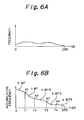
- an axis of abscissa indicates the DR and an axis of ordinate represents the frequency as shown in Figure 6A.
- the frequency distribution table is converted into the accumulative frequency distribution table (step 63).
- the multiplexer 32 selects the address from the address generating circuit 41 and the multiplexer 35 selects the output of the register 36.
- the address is sequentially decreased from 255 to 0.
- the read-out output of the memory 31 is supplied to the adding circuit 34 and is added to the content in the register 36 by the adding circuit 34.
- the output of the adding circuit 34 is written into the same address as the read address of the memory 31.
- the content in the register 36 is updated to the output of the adding circuit 34. In the initial status in which the address in the memory 31 is set to 255, the register 36 has been cleared to zero.
- an accumulative frequency distribution table shown in Figure 6B is formed in the memory 31.
- a generation data amount li when the sets (T1i, T2i, T3i, T4i) of the threshold values in the level direction have been applied to the accumulative frequency distribution table is calculated (step 64).
- the multiplexer 32 selects the output of the address generating circuit 41 and the multiplexer 35 selects the output of the register 36.
- the parameter code generating circuit 39 generates a parameter code which sequentially changes from P1 to P32.
- the parameter codes Pi are supplied to the address generating circuit 41 through the switching circuit 40 and the addresses corresponding to the threshold values of (T1i, T2i, T3i, T4i) are sequentially generated.
- Values A1, A2, A3 and A4 which have been read out of the addresses corresponding to the threshold values are accumulated by the adding circuit 34 and the register 36.
- the accumulative value (A1 + A2 + A3 + A4) corresponds to the generation data amount li when the sets of the threshold values designated by the parameter codes pi have been applied. That is, in the accumulative frequency distribution table shown in Figure 6B, a value in which the number (16) of pixels in the block has been multiplied to the total value (A1 + A2 + A3 + A4) of the values A1, A2, A3, and A4 which had been read out of the addresses respectively corresponding to the threshold values T1, T2, T3, and T4 is equal to the generation data amount (bit length). Since the number of pixels is omitted in the buffering circuit 19 shown in Figure 3.
- the generation data amount li is compared with the target value L/2 (step 65).
- the output of the comparing circuit 37 which is generated when (Ai ⁇ L/2) is satisfied is supplied to the parameter code generating circuit 39.
- the increment of the parameter code Pi is stopped.
- the parameter code Pi from the register 42 and the set of the threshold values generated from the ROM 43 are generated (step 66).
- the buffering to reduce the amount li of data which is generated for the frame F1 by the above operation to L/2 or less is executed.
- the encoding of the two-dimensional ADRC is executed by the threshold values T1 to T4 in the level direction at that time (step 71).
- N1 denotes the number of the threshold value used in the frame F1, that is, the number which coincides with the parameter code Pi of the threshold value used.
- the frame dropping process is executed on a block unit basis by the threshold value M regarding the motion of N1 (step 72).
- the transmission ratio w of the frame F2 after completion of the frame dropping process is detected by the detecting circuit 20 (step 73).
- the data of the frame F2 after completion of the frame dropping process is ADRC encoded (step 74).
- the threshold value at that time is set so as to reduce the generation data amount 12 to L/2 or less in a manner similar to the frame F1.
- the target value L for the 2-frame period is set to the half value, thereby setting the target value L/2 for the one frame period.
- an amount of data to be transmitted is reduced by sub-sampling.
- the number N1 of the threshold value about the frame F1 is large and the number N2 of the threshold value regarding the frame F2 is fairly small.
- a generation data amount 13' when the encoding has been executed by the mean value N3 of the numbers N1 and N2 of the threshold values of the two preceding frames F1 and F2 is obtained (step 75).
- the generation data amount 13' is supplied to the comparing circuit 46 through the register 47.
- the comparing circuit 46 executes a comparing operation of (13' ⁇ L/(1 + w2)) (step 76).
- the data of the frame F3 is encoded by the threshold value of the number N3 (step 77).
- the above relation is not satisfied, it is determined that a scene change occurs.
- the buffering so as to reduce the generation data amount 13 regarding the frame F3 into L/2 or less is performed and the data of the frame F3 is encoded by the threshold value determined by the buffering (step 81).
- the above process is similar to those in the initial status in step 71. The operations similar to those in step 71 and the subsequent steps are repeated hereinbelow.
- step 76 the frame dropping process regarding the frame F4 is executed by the threshold value M3 included in the number N3 of the threshold value (step 78).
- a ratio w4 of the transmission data of the frame F4 after the frame dropping is detected (step 79).
- step 80 The next process of step 80 is similar to that in step 75 and processes similar to those mentioned above are repeated.
- the number of the threshold value can be converged to a mean value shown by a broken line for the frame F3 and subsequent frames.
- the dynamic range DR and the minimum value MIN are transmitted in order to transmit the dynamic range information.
- the maximum value MAX or the quantization step width can be also transmitted as an additional code in place of the dynamic range DR.
- the encoding process has been applied to the pixel data themselves of the block after each 2-frame period.
- the encoding can be also performed to a difference (residual) between each pixel data of the preceding frame and each pixel data of the post frame. That is, in such a case, the data corresponding to the pixels in each block of the post frame has differential value.
- the invention can use a block encoding of a discrete cosine transform (DCT) or the like, instead of ADRC.
- DCT discrete cosine transform
- encoding using the above differential value in place of the pixel data is effective.
- the compression encoding of the ADRC or the like is executed for a two-dimensional block, the necessary memory capacity can be reduced as compared with a three-dimensional block.
- the compression ratio can be raised.
Description
- This invention relates to coding apparatus for digital image signals which apparatus can, for example, be used in a digital video tape recorder (VTR).
- For coding a video signal, methods are known in which a mean number of bits (bit length) per pixel or a sampling frequency is reduced in order to narrow a transmission band. We have proposed coding apparatus in which a dynamic range which is specified by the maximum and minimum values of a plurality of pixels included in a two or three-dimensional block is obtained, and encoding adapted to the dynamic range is executed (Japanese patent specifications JP-A-61-144989 and JP-A-62-92620). Further, as disclosed in Japanese patent specification JP-A-62-128621, there has been proposed a variable length coding method in which the bit length is changed in accordance with the dynamic range, so that the maximum distortion occurring upon quantization is set to be constant.
- According to the above coding method adapted to the dynamic range (ADRC), the dynamic range DR (difference between the maximum value MAX and the minimum value MIN) is calculated for each two-dimensional block comprising, for instance, 64 pixels (= 8 lines x 8 pixels). The minimum level (minimum value) in the block is eliminated from the input pixel data. The pixel data after elimination of the minimum value are converted into a representative level. The quantization includes dividing the dynamic range DR which has been detected into four level ranges corresponding to a bit length such as two bits smaller than the original quantization bit length, for detecting the level range to which each pixel datum in the block belongs, and for generating a code signal indicative of the level range.
- We have also proposed a coding apparatus in which a three-dimensional ADRC and a frame dropping process are combined in order to raise the compression ratio further. In this apparatus, motion between two areas forming a three-dimensional block is detected, three-dimensional ADRC is executed in a block having motion, and in a stationary block, the transmission of one of the areas is omitted and two-dimensional ADRC is executed with respect to a block comprising a mean value of two areas.
- In the above apparatus in which three-dimensional ADRC and frame dropping are combined, memory capacity of two frame is needed for a block segmentation process to form a three-dimensional block. When a buffering process is applied to the above apparatus, a memory of two frames is further necessary to delay input data until the number of bits to be assigned has been decided by the buffering process. A memory capacity of two frames is also needed for a block desegmentation of a decoding apparatus. The total memory capacity required is therefore large.
- European Patent Application No. 87116594.0 (published as EP-A-0267581) discloses a system of coding moving image signals for producing a predictive error signal by a predictive coding based on inter-frame correlation and quantizing by a quantization unit, the produced predictive error signal for each block of a picture frame constituted by N lines of M pixels. The system includes a block coding/non-coding decision unit for calculating a first evaluation value of the predictive error signal for each block of the picture frame and deciding that a block non-coding is applicable when the first evaluation value is less than a first threshold value, and deciding that a block coding is applicable when the first evaluation value is greater than the first threshold value, the predictive error signal not being transmitted when the result of the decision is for a block non-coding, and the predictive error signal being quantized and transmitted when the result of the decision is for a block coding.
- European Patent Application No. 89301739.2 (published as EP-A-0330455) discloses an image encoding apparatus that has a memory for storing image data corresponding to an object for every frame, and a face region detecting circuit for detecting a difference between input frame image data and preceding frame image data, and extracting image data of a face region of the object on the basis of the difference data. More bits are allocated to the extracted face region than those to the remaining image region.
- In accordance with a first aspect of the present invention, there is provided a coding apparatus for a digital image signal, the apparatus comprising: a block segmentor for converting an input digital image signal into a first output signal having a two-dimensional block structure; a circuit for receiving and processing a second output signal, such that between a first and a second block which are located at spatially the same position and respectively belong to a pair of sequential frames of said second output signal, said first and second blocks are transmitted or not transmitted in dependence upon a control signal; a control circuit for generating said control signal; and an encoder to which pixel data of said first block and pixel data of said second block that are to be transmitted are supplied, said encoder compression encoding said pixel data on a block unit basis; said apparatus being characterised in that: said control signal is dependent upon an absolute value of a difference between values of pixel data at the same position between said first and second blocks; said control signal controls said circuit to always transmit said first block and to either transmit or not transmit said second block; and in that there is provided: a sub-sampling circuit for receiving and sub-sampling said first output signal to generate said second output signal, wherein sequential frames of said first output signal are grouped together in pairs and said sub-sampling circuit has a sub-sampling phase that is inverted every sequential pair of frames.
- In accordance with a second aspect of the present invention, there is provided a method of encoding a digital signal, the method comprising: (a) converting an input digital signal into a first output signal having a two-dimensional block structure; (b) grouping sequential frames of said first output signal together in pairs; (c) sub-sampling said first output signal with a sub-sampling phase that is inverted every sequential pair of frames to produce a second output signal; (d) generating a control signal that is dependent upon an absolute value of a difference between values of pixel data at the same position between first and second blocks of sequential pair of frames of said second output signal; (e) processing said second output signal in a circuit (5), such that said first and second blocks are transmitted or not transmitted in dependence upon said control signal, said control signal instructing said circuit (5) to always transmit said first block and selectively transmit or not transmit said second block; and (f) compression encoding pixel data of said first block and pixel data of said second block that are to be transmitted on a block unit basis.
- The invention will now be described by way of example with reference to the accompanying drawings, throughout which like parts are referred to by like references, and in which:
- Figure 1 is a block diagram of an embodiment of the invention;
- Figure 2 is a schematic diagram for explaining sub-sampling;
- Figure 3 is a block diagram of an example of a buffering circuit;
- Figure 4 is a schematic diagram of an example of a threshold value table;
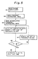
- Figure 5 is a flowchart for explaining the operation of the buffering circuit;
- Figure 6 is a schematic diagram showing a frequency distribution table and an accumulative frequency distribution table which are formed by the buffering circuit;
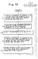
- Figure 7 is a flowchart for explaining the operation of an embodiment; and
- Figure 8 is a schematic diagram for explaining the embodiment.
- Referring to Figure 1, in the embodiment a digital video signal is supplied via an
input terminal 1 to ablock segmentation circuit 2 which converts the video signal from a raster scan into a block signal. That is, a picture plane of one frame is segmented into two-dimensional blocks of, for example, (4 lines x 8 pixels). Unlike three-dimensional blocks, when two-dimensional blocks are formed, the memory capacity of theblock segmentation circuit 2 can be reduced. - An output signal from the
block segmentation circuit 2 is supplied to asub-sampling circuit 3 which halves the number of pixels by a quincunx sub-sampling pattern. Therefore, the number of pixels in one block becomes sixteen. A control signal to cause sub-sampling patterns of complementary forms every two frames is supplied from aterminal 4 to thesub-sampling circuit 3. Motion between the blocks can be detected from a difference of the pixel data of one frame by the sub-sampling. - Figure 2 shows sub-sampling patterns. B1, B2, B3, ... denote blocks which are located spatially at the same position and respectively belong to sequential frames F1, F2, F3, ... A number of blocks other than the blocks shown in the diagram are included in each frame. In Figure 2, ○ and Δ denote transmission pixels, and X indicates non-transmission pixels. In respective two frame periods, such as the frames F1 and F2, the sub-sampling patterns are the same. As shown by partitioning by broken lines, the pattern of two frames and the pattern of the next two frames have complementary shapes.
- An output signal of the
sub-sampling circuit 3 is supplied to aframe dropping circuit 5 to drop frames on a block unit basis, a comparing circuit 6, and a frame delay circuit 7. A control signal to control whether frames should be dropped or not, that is, to control the transmission/non-transmission of the block is supplied to theframe dropping circuit 5 through aswitching circuit 8. Theswitching circuit 8 is controlled by a switching signal from aterminal 9 so as alternately to select input terminals a and b at one frame period. - A signal of "1" is always supplied to the input terminal a of the
switching circuit 8. For theframe dropping circuit 5, "1" denotes that the block is transmitted. Therefore, the blocks B1, B3, B5, ... included in the first frames F1, F3, F5, ... of two sequential frames are always transmitted. In the following frames F2, F4, F6, ..., the input terminal b of theswitching circuit 8 is selected and the transmission/non- transmission is adaptively controlled. That is, the transmission/non-transmission of the block are controlled on the basis of the absolute value of a frame difference between the preceding frame and the present frame. - The comparing circuit 6 detects a frame difference between the values of the pixels of the present frame and the preceding frame. The frame difference is converted into the absolute value by an absolute
value forming circuit 10, an output signal of which is supplied to asumming circuit 11. The absolute value of the frame differences with respect to every two pixels are summed by thesumming circuit 11 for one block. An output of thesumming circuit 11 is supplied to a comparingcircuit 12. - A threshold value M regarding the motion is supplied to the comparing
circuit 12 from abuffering circuit 19, which will be explained below. When the summed value is equal to or smaller than the threshold value M, an output of the comparingcircuit 12 is set to "0". In the other cases, the output of the comparingcircuit 12 is set to "1". In other words, when the summed value is equal to or less than the threshold value M, the frame dropping process in which the block is not terminated is executed. Data corresponding to the motion between the blocks can be derived by other methods. - The output of the comparing
circuit 12 to control the transmission/non-transmission of the block is also supplied to a detectingcircuit 20 to detect a transmission ratio w for one frame period. Since the adaptive frame dropping is executed in the frames F2, F4, ... after every two frames, the transmission ratio w relative to the original data changes in each following frame. Since the total number of blocks in one frame is known, the ratio of the number of blocks which are transmitted to the total number is detected as the transmission ratio w. An output signal of the detectingcircuit 20 is supplied to thebuffering circuit 19. The output signal of the detectingcircuit 20 is also necessary to discriminate the block which has been frame-dropped on the reception side, and is supplied as a frame dropping flag to aframe segmentation circuit 22 and is transmitted together with encoding data, which will be explained below. - An encoder of the ADRC is connected to the
frame dropping circuit 5. Thebuffering circuit 19 is provided in conjunction with the encoder. - An output signal of the
frame dropping circuit 5 is supplied to a detectingcircuit 13 and adelay circuit 14. The detectingcircuit 13 detects the dynamic range DR and the minimum value MIN of the block. Thedelay circuit 14 delays data by a time to detect the minimum value MIN and the dynamic range DR. A subtracting circuit 15 subtracts the minimum value MIN from the video data from thedelay circuit 14, so that the video data from which the minimum value has been eliminated is derived from the subtracting circuit 15. - The output data of the subtracting circuit 15 and the dynamic range DR are supplied to a
quantizing circuit 18 throughdelay circuits circuit 18. The quantizingcircuit 18 executes a quantization adapted to the dynamic range DR. That is, the video data from which the minimum value has been eliminated are divided by a quantization step Δ which is obtained by dividing the dynamic range DR into 2n equal steps. An integral value which is obtained by omitting a fraction of the quotient is used as a code signal DT. The quantizingcircuit 18 can be constructed by a dividing circuit or a ROM. - A bit length n which is assigned to the code signal DT is determined in a manner such that a generation data amount per predetermined period, for instance, every two frames does not exceed a target value L (bits). For such buffering, the
buffering circuit 19 to which the dynamic range DR is supplied is provided. A plurality of, for example, 32 sets (T1, T2, T3, T4, M) of threshold values are prepared for thebuffering circuit 19 as will be explained below. The sets of the threshold values are distinguished by parameter codes Pi (i = 1, 2, 3, ..., 32). The generation data amount is set so as monotonously to decrease as the number i of the parameter code Pi increases. However, the picture quality of the reconstructed image deteriorates with decrease in generation data amount. - The threshold values T1 to T4 in the level direction from the
buffering circuit 19 and the dynamic range DR which has been transmitted through thedelay circuit 17 are supplied to a bitlength deciding circuit 21. Thedelay circuits buffering circuit 19. The dynamic range DR and the threshold values T1 to T4 (T1 < T2 < T3 < T4) are supplied to a bitlength deciding circuit 21. The bit length n to be assigned is determined on the basis of the relations of the magnitudes between the dynamic range DR and the threshold values T1 to T4. - The encoded outputs DR, MIN and DT of the ADRC encoder, the flag indicative of the transmission/non-transmission of the block, and the parameter codes Pi are supplied to the
frame segmentation circuit 22. The transmission data is taken out to an output terminal 23. Theframe segmentation circuit 22 forms the transmission data in which a sync signal has been added to the above encoded outputs. Theframe segmentation circuit 22 also executes an encoding of an error correction code. - Although not shown, on the reproducing side, there are provided a frame desegmentation circuit, a decoder of the ADRC, a circuit to interpolate the frame dropped block by the preceding block, a circuit to interpolate the non-transmission pixels, a block desegmentation circuit, and the like. The ADRC decoder decodes the bit length n by the threshold values T1 to T4 which are designated by the parameter codes Pi and the dynamic range DR, and reconstructs the level by using the quantization step Δ according to the bit length n and the dynamic range DR and the value of the code signal DT. Further, the minimum value MIN is added to the reconstructed level.
- Figure 3 shows an example of the
buffering circuit 19. A memory (RAM) forms a frequency distribution table and an accumulative frequency distribution table. An address is supplied to thememory 31 through amultiplexer 32. The dynamic range DR is supplied as one input of the muliplexer 32 from an input terminal 33 and an address from anaddress generating circuit 41 is supplied as another input. An output signal of an addingcircuit 34 is supplied to thememory 31. Output data of thememory 31 and an output of amultiplexer 35 are added by the addingcircuit 34. - An output of the adding
circuit 34 is supplied to aregister 36. An output of theregister 36 is supplied to themultiplexer 35 and a comparingcircuit 37. In addition to the output of theregister multiplexer 35. When an arithmetic operation of a generation data amount has been performed, a data amount li for one frame period which is generated by the ADRC encoding is obtained in an output of theregister 36. - The comparing
circuit 37 compares the generation data amount li and a target value from a switchingcircuit 38. An output signal of the comparingcircuit 37 is supplied to a parametercode generating circuit 39 and a controlsignal generating circuit 48. The parameter codes Pi from the parametercode generating circuit 39 are supplied through a switching circuit 40 to theaddress generating circuit 41 and aregister 42. The parameter codes Pi taken into theregister 42 are supplied to theframe segmentation circuit 22 as mentioned above and are also supplied to aROM 43. A table of threshold values shown in Figure 4 has been stored in theROM 43. TheROM 43 generates sets (T1i, T2i, T3i, T4i, Mi) of the threshold values in correspondence to the parameter codes Pi which have been input as addresses. The threshold value table is constructed so as to more severely limit the generation data amount as the number of the parameter code Pi increases. That is, the values of the threshold values T1 to T4 in the level direction and the frame dropping threshold value M monotonously increase. As mentioned above, the threshold values in the level direction are supplied to the bitlength deciding circuit 21 and the threshold value M regarding the motion is supplied to the comparingcircuit 12. - The transmission ratio w which has been detected by the detecting
circuit 20 is supplied to anarithmetic operating circuit 45. Assuming that a target value for the generation data amount for a two-frame period of time of F1 and F2 or the like is set to L, thearithmetic operating circuit 45 executes an arithmetic operation of L/(1 + w). The result of the arithmetic operation is supplied to a comparingcircuit 46. An output of thearithmetic operating circuit 45 is used as a target value about the present frame when the mean value of the numbers of the sets of the threshold values for the preceding two-frame period is applied to the present frame. - A generation data amount 1' transmitted through a
register 47 is supplied to the comparingcircuit 46. A comparison output of the comparingcircuit 46 is supplied to the controlsignal generating circuit 48. The generation data amount 1' is derived with respect to the present frame when the mean value of the numbers of the sets of the threshold values for the preceding two-frame period is applied to the present frame. The generation data amount 1' is also supplied to a subtractingcircuit 49. The subtractingcircuit 49 subtracts 1' from a target value L for the 2-frame period. (L - 1') from the subtractingcircuit 49 is supplied to an input terminal d of the switchingcircuit 38. A target value of L/2 is supplied to the other input terminal c of the switchingcircuit 38. - The output signal of the comparing
circuit 46 is supplied to the controlsignal generating circuit 48. - The
control circuit 48 generates control signals to clear theregisters register 50, a signal to control the fetching of the data into theregister 42, and switching signals to respectively control the switchingcircuits 38 and 40. The switchingcircuit 38 supplies the target value of L/2 to the comparingcircuit 37 through the input terminal c in the initial status and upon scene change. In other cases, the switchingcircuit 38 supplies an output signal of the subtractingcircuit 49 to the comparingcircuit 37 as a target value. - The parameter codes Pi from the parameter
code generating circuit 39 are supplied to an input terminal e of the switching circuit 40, theregister 50, and an addingcircuit 51. An output of theregister 50 is supplied to the addingcircuit 51. An output of the addingcircuit 51 is supplied to a 1/2 multiplyingcircuit 52. The number of the mean value of the numbers Ni and Ni + 1 of the threshold values of two sequential frames is generated from the multiplyingcircuit 52. The mean value is supplied to an input terminal f of the switching circuit 40. The switching circuit 40 is controlled by the switching signal from the controlsignal generating circuit 48. When the terminal e of the switching circuit 40 is selected, the parameter codes Pi from the parametercode generating circuit 39 are supplied to theaddress generating circuit 41. On the other hand, when the input terminal f is selected, the parameter codes Pi indicative of the averaged threshold value number are supplied to theaddress generating circuit 41. - In the initial state or just after a scene change has occurred, buffering to control the amount of data generated for one frame period to L/2 or less is executed. That is, in the above case, as shown in Figure 3, the switching
circuit 38 selects the input terminal d and the switching circuit 40 selects theinput terminal 3. The operation of thebuffering circuit 19 in this state will now be described with reference to a flowchart of Figure 5. - In the
first step 61, thememory 31 and theregisters memory 31 to zero, themultiplexer 32 selects the address generated from theaddress generating circuit 41 and the output of the addingcircuit 34 is always set to zero. The address changes to (0, 1, 2, ..., 255) and the zero data is written into all of the addresses in thememory 31. - In the
next step 62, a frequency distribution table of the dynamic range DR of a certain frame as a unit period of time when the buffering is executed is formed in thememory 31. Themultiplexer 32 selects the dynamic range DR from the terminal 33. Themultiplexer 35 selects +1. Therefore, at the end of one frame period, the generation frequency of each DR is stored into each address in thememory 31 corresponding to the dynamic range DR. In the frequency distribution table in thememory 31, an axis of abscissa indicates the DR and an axis of ordinate represents the frequency as shown in Figure 6A. - The frequency distribution table is converted into the accumulative frequency distribution table (step 63). When the accumulative frequency distribution table is formed, the
multiplexer 32 selects the address from theaddress generating circuit 41 and themultiplexer 35 selects the output of theregister 36. The address is sequentially decreased from 255 to 0. The read-out output of thememory 31 is supplied to the addingcircuit 34 and is added to the content in theregister 36 by the addingcircuit 34. The output of the addingcircuit 34 is written into the same address as the read address of thememory 31. The content in theregister 36 is updated to the output of the addingcircuit 34. In the initial status in which the address in thememory 31 is set to 255, theregister 36 has been cleared to zero. When the frequencies have been accumulated with respect to all of the addresses in thememory 31, an accumulative frequency distribution table shown in Figure 6B is formed in thememory 31. - A generation data amount li when the sets (T1i, T2i, T3i, T4i) of the threshold values in the level direction have been applied to the accumulative frequency distribution table is calculated (step 64). When the generation data amount li is calculated, the
multiplexer 32 selects the output of theaddress generating circuit 41 and themultiplexer 35 selects the output of theregister 36. The parametercode generating circuit 39 generates a parameter code which sequentially changes from P1 to P32. The parameter codes Pi are supplied to theaddress generating circuit 41 through the switching circuit 40 and the addresses corresponding to the threshold values of (T1i, T2i, T3i, T4i) are sequentially generated. - Values A1, A2, A3 and A4 which have been read out of the addresses corresponding to the threshold values are accumulated by the adding
circuit 34 and theregister 36. The accumulative value (A1 + A2 + A3 + A4) corresponds to the generation data amount li when the sets of the threshold values designated by the parameter codes pi have been applied. That is, in the accumulative frequency distribution table shown in Figure 6B, a value in which the number (16) of pixels in the block has been multiplied to the total value (A1 + A2 + A3 + A4) of the values A1, A2, A3, and A4 which had been read out of the addresses respectively corresponding to the threshold values T1, T2, T3, and T4 is equal to the generation data amount (bit length). Since the number of pixels is omitted in thebuffering circuit 19 shown in Figure 3. - The generation data amount li is compared with the target value L/2 (step 65). The output of the comparing
circuit 37 which is generated when (Ai ≤ L/2) is satisfied is supplied to the parametercode generating circuit 39. The increment of the parameter code Pi is stopped. The parameter code Pi from theregister 42 and the set of the threshold values generated from theROM 43 are generated (step 66). - If (li ≤ L/2) is not satisfied in discriminating
step 65 in the comparingcircuit 37, the parameter codes Pi are changed to the next parameter codes Pi + 1 and the address corresponding to Pi + 1 is generated from theaddress generating circuit 41. In a manner similar to the above, a generation data amount li + 1 is calculated and compared with the target value L/2 by the comparingcircuit 37. The above operations are repeated until (li ≤ L/2) is satisfied. - The operation of the embodiment will be described with reference to Figure 7. In the initial state in which the image data of the first frame F1 shown in Figure 2 is input, the buffering to reduce the amount li of data which is generated for the frame F1 by the above operation to L/2 or less is executed. The encoding of the two-dimensional ADRC is executed by the threshold values T1 to T4 in the level direction at that time (step 71). N1 denotes the number of the threshold value used in the frame F1, that is, the number which coincides with the parameter code Pi of the threshold value used.
- In the next frame F2, the frame dropping process is executed on a block unit basis by the threshold value M regarding the motion of N1 (step 72). The transmission ratio w of the frame F2 after completion of the frame dropping process is detected by the detecting circuit 20 (step 73). The data of the frame F2 after completion of the frame dropping process is ADRC encoded (step 74). The threshold value at that time is set so as to reduce the generation data amount 12 to L/2 or less in a manner similar to the frame F1.
- With respect to the frames F1 and F2, the target value L for the 2-frame period is set to the half value, thereby setting the target value L/2 for the one frame period. For the frame F2, however, an amount of data to be transmitted is reduced by sub-sampling. Thus, as shown in Figure 8, the number N1 of the threshold value about the frame F1 is large and the number N2 of the threshold value regarding the frame F2 is fairly small.
- After an accumulative frequency distribution table was formed with regard to the next frame F3, a generation data amount 13' when the encoding has been executed by the mean value N3 of the numbers N1 and N2 of the threshold values of the two preceding frames F1 and F2 is obtained (step 75). The generation data amount 13' is supplied to the comparing
circuit 46 through theregister 47. The comparingcircuit 46 executes a comparing operation of (13' ≤ L/(1 + w2)) (step 76). - When the above relation is satisfied, the data of the frame F3 is encoded by the threshold value of the number N3 (step 77). On the contrary, when the above relation is not satisfied, it is determined that a scene change occurs. The buffering so as to reduce the generation data amount 13 regarding the frame F3 into L/2 or less is performed and the data of the frame F3 is encoded by the threshold value determined by the buffering (step 81). The above process is similar to those in the initial status in
step 71. The operations similar to those instep 71 and the subsequent steps are repeated hereinbelow. - When the relation in
step 76 is satisfied, the frame dropping process regarding the frame F4 is executed by the threshold value M3 included in the number N3 of the threshold value (step 78). A ratio w4 of the transmission data of the frame F4 after the frame dropping is detected (step 79). - In the buffering about the frame F4, (L - 13') formed by the subtracting
circuit 49, is used as a target value. That is, in the preceding frame F3, since the data of 13' has been generated for the target value L for the 2-frame period, the generation data amount of the frame F4 is suppressed to a value which is equal to or less than the remaining data amount of (L - 13'). The data of the frame F4 is encoded by the number N4 of the threshold value determined by the buffering (step 80). The next process ofstep 80 is similar to that in step 75 and processes similar to those mentioned above are repeated. - In the embodiment in which the above operations are executed, when a scene change does not occur, as shown in Figure 8, the number of the threshold value can be converged to a mean value shown by a broken line for the frame F3 and subsequent frames.
- In the above description, the dynamic range DR and the minimum value MIN are transmitted in order to transmit the dynamic range information. However, the maximum value MAX or the quantization step width can be also transmitted as an additional code in place of the dynamic range DR.
- On the other hand, in the above embodiment, the encoding process has been applied to the pixel data themselves of the block after each 2-frame period. However, the encoding can be also performed to a difference (residual) between each pixel data of the preceding frame and each pixel data of the post frame. That is, in such a case, the data corresponding to the pixels in each block of the post frame has differential value.
- The invention, further, can use a block encoding of a discrete cosine transform (DCT) or the like, instead of ADRC. In the case of DCT, encoding using the above differential value in place of the pixel data is effective.
- Since the compression encoding of the ADRC or the like is executed for a two-dimensional block, the necessary memory capacity can be reduced as compared with a three-dimensional block. On the other hand, since there is used a hybrid construction of the frame dropping on a block unit basis and the compression encoding, the compression ratio can be raised.
Claims (9)
- A coding apparatus for a digital image signal, the apparatus comprising:a block segmentor (2) for converting an input digital image signal into a first output signal having a two-dimensional block structure;a circuit (5) for receiving and processing a second output signal, such that between a first and a second block which are located at spatially the same position and respectively belong to a pair of sequential frames of said second output signal, said first and second blocks are transmitted or not transmitted in dependence upon a control signal;a control circuit (6 to 12) for generating said control signal; andan encoder (18) to which pixel data of said first block and pixel data of said second block that are to be transmitted are supplied, said encoder (18) compression encoding said pixel data on a block unit basis;said apparatus being characterised in that:said control signal is dependent upon an absolute value of a difference between values of pixel data at the same position between said first and second blocks;said control signal controls said circuit (5) to always transmit said first block and to either transmit or not transmit said second block; andin that there is provided:a sub-sampling circuit (3) for receiving and sub-sampling said first output signal to generate said second output signal, wherein sequential frames of said first output signal are grouped in pairs and said sub-sampling circuit (3) has a sub-sampling phase that is inverted every sequential pair of frames.
- A coding apparatus according to Claim 1, further comprising a buffering circuit (19) which controls said compression encoding, said encoding being accomplished in a two-step process such that a data amount for a two-frame period is equal to or less than a target value "L", said two-step process comprising:(a) processing a preceding pair of frames with reference to a predetermined threshold level to generate a mean threshold for said preceding frames and applying said mean threshold to said first frame of said two frame period to generate an amount of data "1"' for said first frame; and(b) buffering said second frame of said two frame period to limit an amount of data generated for said second frame to a value equal to or less than "(L-1')".
- A coding apparatus according to Claim 2 wherein the buffering circuit (19) initially limits the generation data amount for one frame period to a value equal to or less than "L/2".
- A coding apparatus according to Claim 2 or Claim 3 wherein said buffering circuit (19) includes a scene change detector (37), a scene change being detected if a generation data amount for said first frame exceeds a value dependent upon the target value for that first frame and a transmission ratio of a preceding frame.
- A coding apparatus according to Claim 4 wherein the buffering circuit (19) limits the generation data amount for one frame period to a value equal to or less than "L/2" when a scene change is detected.
- A coding apparatus according to Claim 2 wherein said buffering circuit (19) controls the amount of data generated with first and second threshold values, said threshold values being provided in a threshold value table (43), said first threshold values being defined in a level direction and said second threshold values being provided for controlling the transmission/non-transmission of the second block.
- A coding apparatus according to any one of the preceding claims wherein difference data is generated for each pixel of said first and second blocks, said difference data being equal to the difference between respective pixels of said first and second blocks, said difference data subsequently being used as pixel data for said second block.
- A coding apparatus according to any one of the preceding claims wherein said encoder (18) executes a quantization with a bit length shorter than an original bit length so as to be adaptive to a dynamic range equal to a difference between maximum and minimum values of each of said blocks.
- A method of encoding a digital signal, the method comprising:(a) converting an input digital signal into a first output signal having a two-dimensional block structure;(b) grouping sequential frames of said first output signal together in pairs;(c) sub-sampling said first output signal with a sub-sampling phase that is inverted every sequential pair of frames to produce a second output signal;(d) generating a control signal that is dependent upon an absolute value of a difference between values of pixel data at the same position between first and second blocks of a pair of sequential frames of said second output signal;(e) processing said second output signal in a circuit (5), such that said first and second blocks are transmitted or not transmitted in dependence upon said control signal, said control signal instructing said circuit (5) to always transmit said first block and selectively transmit or not transmit said second block; and(f) compression encoding pixel data of said first block and pixel data of said second block that are to be transmitted on a block unit basis.
Applications Claiming Priority (2)
| Application Number | Priority Date | Filing Date | Title |
|---|---|---|---|
| JP231535/90 | 1990-08-31 | ||
| JP23153590A JP2969867B2 (en) | 1990-08-31 | 1990-08-31 | High-efficiency encoder for digital image signals. |
Publications (3)
| Publication Number | Publication Date |
|---|---|
| EP0473384A2 EP0473384A2 (en) | 1992-03-04 |
| EP0473384A3 EP0473384A3 (en) | 1993-03-03 |
| EP0473384B1 true EP0473384B1 (en) | 1997-07-09 |
Family
ID=16925018
Family Applications (1)
| Application Number | Title | Priority Date | Filing Date |
|---|---|---|---|
| EP19910307804 Expired - Lifetime EP0473384B1 (en) | 1990-08-31 | 1991-08-23 | Coding apparatus for digital image signals |
Country Status (5)
| Country | Link |
|---|---|
| US (1) | US5241381A (en) |
| EP (1) | EP0473384B1 (en) |
| JP (1) | JP2969867B2 (en) |
| KR (1) | KR0185583B1 (en) |
| DE (1) | DE69126750T2 (en) |
Families Citing this family (77)
| Publication number | Priority date | Publication date | Assignee | Title |
|---|---|---|---|---|
| JPH0556418A (en) * | 1991-08-28 | 1993-03-05 | Sharp Corp | Picture encoder device |
| JPH05103212A (en) * | 1991-10-03 | 1993-04-23 | Sony Corp | Data transmission equipment |
| US5686961A (en) * | 1992-01-27 | 1997-11-11 | Harris Corporation | Automatic video image data reduction and prioritization system and method |
| JPH0614313A (en) * | 1992-06-29 | 1994-01-21 | Canon Inc | Image processor |
| JP3315766B2 (en) * | 1992-09-07 | 2002-08-19 | 富士通株式会社 | Image data encoding method, image data encoding device using the method, image data restoring method, image data restoring device using the method, scene change detecting method, scene change detecting device using the method, scene change recording Device and image data scene change recording / reproducing device |
| US5850261A (en) * | 1992-10-15 | 1998-12-15 | Sony Corporation | Efficient variable length encoder and decoder |
| JPH06165151A (en) * | 1992-11-25 | 1994-06-10 | Matsushita Electric Ind Co Ltd | Device for controlling video coding quantity |
| JPH1032495A (en) * | 1996-07-18 | 1998-02-03 | Sony Corp | Device and method for processing data |
| US5956083A (en) * | 1996-10-29 | 1999-09-21 | Eastman Kodak Company | Camera and method for capturing motion sequences useful for integral image element formation |
| US6775417B2 (en) * | 1997-10-02 | 2004-08-10 | S3 Graphics Co., Ltd. | Fixed-rate block-based image compression with inferred pixel values |
| US6311297B1 (en) * | 1997-10-23 | 2001-10-30 | Sony Corporation | Apparatus and method for mapping an image to blocks to provide for robust error recovery in a lossy transmission environment |
| US6581170B1 (en) | 1997-10-23 | 2003-06-17 | Sony Corporation | Source coding to provide for robust error recovery during transmission losses |
| US6282684B1 (en) | 1997-10-23 | 2001-08-28 | Sony Corporation | Apparatus and method for recovery of data in a lossy transmission environment |
| US6741651B1 (en) * | 1998-01-21 | 2004-05-25 | Matsushita Electric Industrial Co., Ltd. | Variable-length encoder |
| US6621936B1 (en) | 1999-02-12 | 2003-09-16 | Sony Corporation | Method and apparatus for spatial class reduction |
| US6307560B1 (en) | 1999-02-12 | 2001-10-23 | Sony Corporation | Classified adaptive spatio-temporal format conversion method and apparatus |
| US6535148B1 (en) | 1999-02-12 | 2003-03-18 | Sony Corporation | Method and apparatus for truncated decoding |
| US6591398B1 (en) | 1999-02-12 | 2003-07-08 | Sony Corporation | Multiple processing system |
| US6154761A (en) * | 1999-02-12 | 2000-11-28 | Sony Corporation | Classified adaptive multiple processing system |
| US6192161B1 (en) | 1999-02-12 | 2001-02-20 | Sony Corporation | Method and apparatus for adaptive filter tap selection according to a class |
| US6170074B1 (en) | 1999-02-12 | 2001-01-02 | Sony Corporation | Source coding to provide for robust error recovery |
| US6178266B1 (en) * | 1999-02-12 | 2001-01-23 | Sony Corporation | Method and apparatus for the recovery of compression constants in the encoded domain |
| US6519369B1 (en) | 1999-02-12 | 2003-02-11 | Sony Corporation | Method and apparatus for filter tap expansion |
| US7010737B2 (en) * | 1999-02-12 | 2006-03-07 | Sony Corporation | Method and apparatus for error data recovery |
| US6307979B1 (en) | 1999-02-12 | 2001-10-23 | Sony Corporation | Classified adaptive error recovery method and apparatus |
| US6363118B1 (en) | 1999-02-12 | 2002-03-26 | Sony Corporation | Apparatus and method for the recovery of compression constants in the encoded domain |
| US6151416A (en) * | 1999-02-12 | 2000-11-21 | Sony Corporation | Method and apparatus for adaptive class tap selection according to multiple classification |
| US6697489B1 (en) | 1999-03-30 | 2004-02-24 | Sony Corporation | Method and apparatus for securing control words |
| US7565546B2 (en) | 1999-03-30 | 2009-07-21 | Sony Corporation | System, method and apparatus for secure digital content transmission |
| US7730300B2 (en) | 1999-03-30 | 2010-06-01 | Sony Corporation | Method and apparatus for protecting the transfer of data |
| US6473876B1 (en) | 1999-06-29 | 2002-10-29 | Sony Corporation | Method and apparatus for encoding of bitstreams using rotation |
| US6389562B1 (en) | 1999-06-29 | 2002-05-14 | Sony Corporation | Source code shuffling to provide for robust error recovery |
| US6549672B1 (en) * | 1999-06-29 | 2003-04-15 | Sony Corporation | Method and apparatus for recovery of encoded data using central value |
| US6493842B1 (en) | 1999-06-29 | 2002-12-10 | Sony Corporation | Time-varying randomization for data synchronization and implicit information transmission |
| US6351494B1 (en) | 1999-09-24 | 2002-02-26 | Sony Corporation | Classified adaptive error recovery method and apparatus |
| US6522785B1 (en) | 1999-09-24 | 2003-02-18 | Sony Corporation | Classified adaptive error recovery method and apparatus |
| US7039614B1 (en) | 1999-11-09 | 2006-05-02 | Sony Corporation | Method for simulcrypting scrambled data to a plurality of conditional access devices |
| US6539517B1 (en) | 1999-11-09 | 2003-03-25 | Sony Corporation | Data transformation for explicit transmission of control information |
| US7225164B1 (en) | 2000-02-15 | 2007-05-29 | Sony Corporation | Method and apparatus for implementing revocation in broadcast networks |
| US20030206631A1 (en) * | 2000-06-22 | 2003-11-06 | Candelore Brant L. | Method and apparatus for scrambling program data for furture viewing |
| US7895616B2 (en) | 2001-06-06 | 2011-02-22 | Sony Corporation | Reconstitution of program streams split across multiple packet identifiers |
| US7747853B2 (en) | 2001-06-06 | 2010-06-29 | Sony Corporation | IP delivery of secure digital content |
| US7124303B2 (en) | 2001-06-06 | 2006-10-17 | Sony Corporation | Elementary stream partial encryption |
| US7350082B2 (en) | 2001-06-06 | 2008-03-25 | Sony Corporation | Upgrading of encryption |
| US7215770B2 (en) | 2002-01-02 | 2007-05-08 | Sony Corporation | System and method for partially encrypted multimedia stream |
| US7155012B2 (en) | 2002-01-02 | 2006-12-26 | Sony Corporation | Slice mask and moat pattern partial encryption |
| US7823174B2 (en) | 2002-01-02 | 2010-10-26 | Sony Corporation | Macro-block based content replacement by PID mapping |
| US7302059B2 (en) | 2002-01-02 | 2007-11-27 | Sony Corporation | Star pattern partial encryption |
| US7765567B2 (en) | 2002-01-02 | 2010-07-27 | Sony Corporation | Content replacement by PID mapping |
| US7039938B2 (en) | 2002-01-02 | 2006-05-02 | Sony Corporation | Selective encryption for video on demand |
| US7376233B2 (en) | 2002-01-02 | 2008-05-20 | Sony Corporation | Video slice and active region based multiple partial encryption |
| US7218738B2 (en) | 2002-01-02 | 2007-05-15 | Sony Corporation | Encryption and content control in a digital broadcast system |
| US7233669B2 (en) | 2002-01-02 | 2007-06-19 | Sony Corporation | Selective encryption to enable multiple decryption keys |
| US7292691B2 (en) | 2002-01-02 | 2007-11-06 | Sony Corporation | Progressive video refresh slice detection |
| US7242773B2 (en) | 2002-09-09 | 2007-07-10 | Sony Corporation | Multiple partial encryption using retuning |
| US7530084B2 (en) | 2002-05-28 | 2009-05-05 | Sony Corporation | Method and apparatus for synchronizing dynamic graphics |
| US8818896B2 (en) | 2002-09-09 | 2014-08-26 | Sony Corporation | Selective encryption with coverage encryption |
| US8572408B2 (en) | 2002-11-05 | 2013-10-29 | Sony Corporation | Digital rights management of a digital device |
| US7724907B2 (en) | 2002-11-05 | 2010-05-25 | Sony Corporation | Mechanism for protecting the transfer of digital content |
| US8645988B2 (en) | 2002-12-13 | 2014-02-04 | Sony Corporation | Content personalization for digital content |
| US8667525B2 (en) | 2002-12-13 | 2014-03-04 | Sony Corporation | Targeted advertisement selection from a digital stream |
| US20040165586A1 (en) * | 2003-02-24 | 2004-08-26 | Read Christopher Jensen | PID filters based network routing |
| US7409702B2 (en) | 2003-03-20 | 2008-08-05 | Sony Corporation | Auxiliary program association table |
| US7292692B2 (en) | 2003-03-25 | 2007-11-06 | Sony Corporation | Content scrambling with minimal impact on legacy devices |
| US7286667B1 (en) | 2003-09-15 | 2007-10-23 | Sony Corporation | Decryption system |
| US7853980B2 (en) | 2003-10-31 | 2010-12-14 | Sony Corporation | Bi-directional indices for trick mode video-on-demand |
| US7263187B2 (en) | 2003-10-31 | 2007-08-28 | Sony Corporation | Batch mode session-based encryption of video on demand content |
| US7343013B2 (en) | 2003-12-16 | 2008-03-11 | Sony Corporation | Composite session-based encryption of video on demand content |
| US7346163B2 (en) | 2003-10-31 | 2008-03-18 | Sony Corporation | Dynamic composition of pre-encrypted video on demand content |
| US7620180B2 (en) | 2003-11-03 | 2009-11-17 | Sony Corporation | Preparation of content for multiple conditional access methods in video on demand |
| US7466867B2 (en) * | 2004-11-26 | 2008-12-16 | Taiwan Imagingtek Corporation | Method and apparatus for image compression and decompression |
| US8041190B2 (en) | 2004-12-15 | 2011-10-18 | Sony Corporation | System and method for the creation, synchronization and delivery of alternate content |
| US7895617B2 (en) | 2004-12-15 | 2011-02-22 | Sony Corporation | Content substitution editor |
| JP4169768B2 (en) * | 2006-02-24 | 2008-10-22 | 三菱電機株式会社 | Image coding apparatus, image processing apparatus, image coding method, and image processing method |
| US8185921B2 (en) | 2006-02-28 | 2012-05-22 | Sony Corporation | Parental control of displayed content using closed captioning |
| US7555464B2 (en) | 2006-03-01 | 2009-06-30 | Sony Corporation | Multiple DRM management |
| US20110069225A1 (en) * | 2009-09-24 | 2011-03-24 | Sensio Technologies Inc. | Method and system for transmitting and processing high definition digital video signals |
Citations (1)
| Publication number | Priority date | Publication date | Assignee | Title |
|---|---|---|---|---|
| EP0267581A2 (en) * | 1986-11-10 | 1988-05-18 | Kokusai Denshin Denwa Co., Ltd | Moving image signal coding system |
Family Cites Families (9)
| Publication number | Priority date | Publication date | Assignee | Title |
|---|---|---|---|---|
| JPS60189388A (en) * | 1984-03-09 | 1985-09-26 | Fujitsu Ltd | Moving compensation encoder |
| JP2540809B2 (en) * | 1986-07-30 | 1996-10-09 | ソニー株式会社 | High efficiency encoder |
| JP2508439B2 (en) * | 1987-05-29 | 1996-06-19 | ソニー株式会社 | High efficiency encoder |
| GB8724789D0 (en) * | 1987-10-19 | 1987-11-25 | British Telecomm | Signal coding |
| EP0330455A3 (en) * | 1988-02-22 | 1990-07-04 | Kabushiki Kaisha Toshiba | Image encoding apparatus |
| JP3251002B2 (en) * | 1989-08-15 | 2002-01-28 | ソニー株式会社 | Apparatus and method for receiving image data |
| JP2827356B2 (en) * | 1989-11-28 | 1998-11-25 | ソニー株式会社 | Image signal transmission apparatus and method |
| US4980767A (en) * | 1989-11-30 | 1990-12-25 | At&T Bell Laboratories | Technique for determining signal dispersion characteristics in communications systems |
| US5128759A (en) * | 1990-05-31 | 1992-07-07 | Sony Corporation | Video signal decoder |
-
1990
- 1990-08-31 JP JP23153590A patent/JP2969867B2/en not_active Expired - Lifetime
-
1991
- 1991-08-16 US US07/745,855 patent/US5241381A/en not_active Expired - Lifetime
- 1991-08-23 DE DE1991626750 patent/DE69126750T2/en not_active Expired - Lifetime
- 1991-08-23 EP EP19910307804 patent/EP0473384B1/en not_active Expired - Lifetime
- 1991-08-28 KR KR1019910014923A patent/KR0185583B1/en not_active IP Right Cessation
Patent Citations (1)
| Publication number | Priority date | Publication date | Assignee | Title |
|---|---|---|---|---|
| EP0267581A2 (en) * | 1986-11-10 | 1988-05-18 | Kokusai Denshin Denwa Co., Ltd | Moving image signal coding system |
Also Published As
| Publication number | Publication date |
|---|---|
| EP0473384A2 (en) | 1992-03-04 |
| DE69126750T2 (en) | 1997-10-23 |
| EP0473384A3 (en) | 1993-03-03 |
| JP2969867B2 (en) | 1999-11-02 |
| JPH04115686A (en) | 1992-04-16 |
| US5241381A (en) | 1993-08-31 |
| DE69126750D1 (en) | 1997-08-14 |
| KR0185583B1 (en) | 1999-04-15 |
Similar Documents
| Publication | Publication Date | Title |
|---|---|---|
| EP0473384B1 (en) | Coding apparatus for digital image signals | |
| USRE36380E (en) | Orthogonal transform coding apparatus | |
| CA2011034C (en) | A highly efficient coding apparatus | |
| US4722003A (en) | High efficiency coding apparatus | |
| US4845560A (en) | High efficiency coding apparatus | |
| US5073821A (en) | Orthogonal transform coding apparatus for reducing the amount of coded signals to be processed and transmitted | |
| US5263100A (en) | Image coding method and apparatus | |
| US5193003A (en) | Apparatus for decoding digital video data with small memory requirement | |
| US4802005A (en) | High efficiency encoding system | |
| EP0399487B1 (en) | Transformation coding device | |
| US5251030A (en) | MC predicting apparatus | |
| GB2128847A (en) | A motion-compensated interframe coding system | |
| US5068726A (en) | Coding apparatus that temporally interpolates block data and selects transmission mode | |
| US5389973A (en) | Quantization control circuit | |
| US5982439A (en) | Coding image data | |
| US6473465B1 (en) | Method and apparatus for video coding at high efficiency | |
| US5907636A (en) | Image signal decoder | |
| EP0417914B1 (en) | Decoding and coding apparatus for compressed digital video data | |
| US5703648A (en) | Coding apparatus | |
| CA2166623C (en) | Coding image data | |
| JP3178233B2 (en) | Image encoding method, image encoding device, and optical disk | |
| US20010043653A1 (en) | Method and apparatus for image encoding method and appartus for image decoding and recording medium | |
| JP2777171B2 (en) | Video motion compensation method | |
| JP2990768B2 (en) | High-efficiency encoder for digital image signals. | |
| JP3191433B2 (en) | High efficiency coding device |
Legal Events
| Date | Code | Title | Description |
|---|---|---|---|
| PUAI | Public reference made under article 153(3) epc to a published international application that has entered the european phase |
Free format text: ORIGINAL CODE: 0009012 |
|
| AK | Designated contracting states |
Kind code of ref document: A2 Designated state(s): DE FR GB |
|
| PUAL | Search report despatched |
Free format text: ORIGINAL CODE: 0009013 |
|
| AK | Designated contracting states |
Kind code of ref document: A3 Designated state(s): DE FR GB |
|
| 17P | Request for examination filed |
Effective date: 19930803 |
|
| 17Q | First examination report despatched |
Effective date: 19950809 |
|
| GRAG | Despatch of communication of intention to grant |
Free format text: ORIGINAL CODE: EPIDOS AGRA |
|
| GRAH | Despatch of communication of intention to grant a patent |
Free format text: ORIGINAL CODE: EPIDOS IGRA |
|
| GRAH | Despatch of communication of intention to grant a patent |
Free format text: ORIGINAL CODE: EPIDOS IGRA |
|
| GRAA | (expected) grant |
Free format text: ORIGINAL CODE: 0009210 |
|
| AK | Designated contracting states |
Kind code of ref document: B1 Designated state(s): DE FR GB |
|
| REF | Corresponds to: |
Ref document number: 69126750 Country of ref document: DE Date of ref document: 19970814 |
|
| ET | Fr: translation filed | ||
| PLBE | No opposition filed within time limit |
Free format text: ORIGINAL CODE: 0009261 |
|
| STAA | Information on the status of an ep patent application or granted ep patent |
Free format text: STATUS: NO OPPOSITION FILED WITHIN TIME LIMIT |
|
| 26N | No opposition filed | ||
| REG | Reference to a national code |
Ref country code: GB Ref legal event code: IF02 |
|
| REG | Reference to a national code |
Ref country code: GB Ref legal event code: 746 Effective date: 20091124 |
|
| PGFP | Annual fee paid to national office [announced via postgrant information from national office to epo] |
Ref country code: FR Payment date: 20100901 Year of fee payment: 20 Ref country code: DE Payment date: 20100823 Year of fee payment: 20 |
|
| PGFP | Annual fee paid to national office [announced via postgrant information from national office to epo] |
Ref country code: GB Payment date: 20100819 Year of fee payment: 20 |
|
| REG | Reference to a national code |
Ref country code: DE Ref legal event code: R071 Ref document number: 69126750 Country of ref document: DE |
|
| REG | Reference to a national code |
Ref country code: DE Ref legal event code: R071 Ref document number: 69126750 Country of ref document: DE |
|
| PG25 | Lapsed in a contracting state [announced via postgrant information from national office to epo] |
Ref country code: GB Free format text: LAPSE BECAUSE OF EXPIRATION OF PROTECTION Effective date: 20110822 |
|
| PG25 | Lapsed in a contracting state [announced via postgrant information from national office to epo] |
Ref country code: DE Free format text: LAPSE BECAUSE OF EXPIRATION OF PROTECTION Effective date: 20110824 |