EP0451984B1 - Ultrasonic probe system - Google Patents
Ultrasonic probe system Download PDFInfo
- Publication number
- EP0451984B1 EP0451984B1 EP91302583A EP91302583A EP0451984B1 EP 0451984 B1 EP0451984 B1 EP 0451984B1 EP 91302583 A EP91302583 A EP 91302583A EP 91302583 A EP91302583 A EP 91302583A EP 0451984 B1 EP0451984 B1 EP 0451984B1
- Authority
- EP
- European Patent Office
- Prior art keywords
- layers
- piezoelectric
- electrode
- ultrasonic
- stacked
- Prior art date
- Legal status (The legal status is an assumption and is not a legal conclusion. Google has not performed a legal analysis and makes no representation as to the accuracy of the status listed.)
- Expired - Lifetime
Links
- 239000000523 sample Substances 0.000 title claims description 70
- 230000010287 polarization Effects 0.000 claims description 58
- 230000005684 electric field Effects 0.000 claims description 19
- 238000006243 chemical reaction Methods 0.000 claims description 2
- 239000010410 layer Substances 0.000 description 113
- 238000000034 method Methods 0.000 description 11
- 238000010586 diagram Methods 0.000 description 7
- 230000005540 biological transmission Effects 0.000 description 6
- 230000035945 sensitivity Effects 0.000 description 5
- 239000000919 ceramic Substances 0.000 description 4
- 230000004048 modification Effects 0.000 description 4
- 238000012986 modification Methods 0.000 description 4
- 238000001228 spectrum Methods 0.000 description 4
- 238000012360 testing method Methods 0.000 description 3
- 230000017531 blood circulation Effects 0.000 description 2
- 229910010293 ceramic material Inorganic materials 0.000 description 2
- 230000008859 change Effects 0.000 description 2
- 238000005520 cutting process Methods 0.000 description 2
- 230000003247 decreasing effect Effects 0.000 description 2
- 230000000694 effects Effects 0.000 description 2
- 230000001747 exhibiting effect Effects 0.000 description 2
- 238000004519 manufacturing process Methods 0.000 description 2
- 239000000463 material Substances 0.000 description 2
- 238000005259 measurement Methods 0.000 description 2
- 230000005855 radiation Effects 0.000 description 2
- 230000007306 turnover Effects 0.000 description 2
- 230000004075 alteration Effects 0.000 description 1
- 210000000601 blood cell Anatomy 0.000 description 1
- 210000001715 carotid artery Anatomy 0.000 description 1
- 230000008878 coupling Effects 0.000 description 1
- 238000010168 coupling process Methods 0.000 description 1
- 238000005859 coupling reaction Methods 0.000 description 1
- 230000001186 cumulative effect Effects 0.000 description 1
- 238000011161 development Methods 0.000 description 1
- 238000003745 diagnosis Methods 0.000 description 1
- 238000002592 echocardiography Methods 0.000 description 1
- 238000003384 imaging method Methods 0.000 description 1
- 230000006872 improvement Effects 0.000 description 1
- 210000003734 kidney Anatomy 0.000 description 1
- 210000004185 liver Anatomy 0.000 description 1
- 238000013507 mapping Methods 0.000 description 1
- 239000002184 metal Substances 0.000 description 1
- 230000002969 morbid Effects 0.000 description 1
- 230000010355 oscillation Effects 0.000 description 1
- 210000000496 pancreas Anatomy 0.000 description 1
- 230000035515 penetration Effects 0.000 description 1
- 238000012545 processing Methods 0.000 description 1
- 230000002035 prolonged effect Effects 0.000 description 1
- 239000002356 single layer Substances 0.000 description 1
- 210000004291 uterus Anatomy 0.000 description 1
- 210000001835 viscera Anatomy 0.000 description 1
- XLYOFNOQVPJJNP-UHFFFAOYSA-N water Substances O XLYOFNOQVPJJNP-UHFFFAOYSA-N 0.000 description 1
Images


Classifications
-
- B—PERFORMING OPERATIONS; TRANSPORTING
- B06—GENERATING OR TRANSMITTING MECHANICAL VIBRATIONS IN GENERAL
- B06B—METHODS OR APPARATUS FOR GENERATING OR TRANSMITTING MECHANICAL VIBRATIONS OF INFRASONIC, SONIC, OR ULTRASONIC FREQUENCY, e.g. FOR PERFORMING MECHANICAL WORK IN GENERAL
- B06B1/00—Methods or apparatus for generating mechanical vibrations of infrasonic, sonic, or ultrasonic frequency
- B06B1/02—Methods or apparatus for generating mechanical vibrations of infrasonic, sonic, or ultrasonic frequency making use of electrical energy
- B06B1/06—Methods or apparatus for generating mechanical vibrations of infrasonic, sonic, or ultrasonic frequency making use of electrical energy operating with piezoelectric effect or with electrostriction
- B06B1/0607—Methods or apparatus for generating mechanical vibrations of infrasonic, sonic, or ultrasonic frequency making use of electrical energy operating with piezoelectric effect or with electrostriction using multiple elements
- B06B1/0611—Methods or apparatus for generating mechanical vibrations of infrasonic, sonic, or ultrasonic frequency making use of electrical energy operating with piezoelectric effect or with electrostriction using multiple elements in a pile
- B06B1/0614—Methods or apparatus for generating mechanical vibrations of infrasonic, sonic, or ultrasonic frequency making use of electrical energy operating with piezoelectric effect or with electrostriction using multiple elements in a pile for generating several frequencies
-
- B—PERFORMING OPERATIONS; TRANSPORTING
- B06—GENERATING OR TRANSMITTING MECHANICAL VIBRATIONS IN GENERAL
- B06B—METHODS OR APPARATUS FOR GENERATING OR TRANSMITTING MECHANICAL VIBRATIONS OF INFRASONIC, SONIC, OR ULTRASONIC FREQUENCY, e.g. FOR PERFORMING MECHANICAL WORK IN GENERAL
- B06B1/00—Methods or apparatus for generating mechanical vibrations of infrasonic, sonic, or ultrasonic frequency
- B06B1/02—Methods or apparatus for generating mechanical vibrations of infrasonic, sonic, or ultrasonic frequency making use of electrical energy
- B06B1/06—Methods or apparatus for generating mechanical vibrations of infrasonic, sonic, or ultrasonic frequency making use of electrical energy operating with piezoelectric effect or with electrostriction
- B06B1/0607—Methods or apparatus for generating mechanical vibrations of infrasonic, sonic, or ultrasonic frequency making use of electrical energy operating with piezoelectric effect or with electrostriction using multiple elements
- B06B1/0622—Methods or apparatus for generating mechanical vibrations of infrasonic, sonic, or ultrasonic frequency making use of electrical energy operating with piezoelectric effect or with electrostriction using multiple elements on one surface
- B06B1/064—Methods or apparatus for generating mechanical vibrations of infrasonic, sonic, or ultrasonic frequency making use of electrical energy operating with piezoelectric effect or with electrostriction using multiple elements on one surface with multiple active layers
Definitions
- the present invention relates to an ultrasonic probe used for an ultrasonic test apparatus and, more particularly, to an ultrasonic probe system which is constituted by a stacked piezoelectric element and is capable of transmitting/receiving ultrasonic waves having different frequencies.
- An ultrasonic probe has a probe head mainly constituted by a piezoelectric element. This ultrasonic probe is used to obtain image data representing the internal state of a target object by radiating ultrasonic waves onto the target object and immediately receiving waves reflected from interfaces of the target object which have different acoustic impedances.
- An ultrasonic test apparatus using such an ultrasonic probe is used in practice as, e.g., a medical diagnosing apparatus for examining the inside of a human body, or an industrial test apparatus for inspecting flaws in welded metal portions.
- the above-mentioned B mode image i.e., a tomographic image of a human body
- a high-resolution image be obtained with high sensitivity to allow an operator to clearly observe a physical change or a cavity as a slight morbid alteration.
- the Doppler mode for acquiring a CFM image or the like since echoes (waves) reflected by, e.g., microscopic blood cells, each having a diameter of several »m, are used, the resulting signal level is lower than that obtained in the B mode described above. For this reason, high-sensitivity performance is especially required.
- a reference frequency in this Doppler mode is set to be lower than the center frequency in the frequency band of an ultrasonic probe.
- duplex type ultrasonic probes are available from various manufacturers.
- a duplex type ultrasonic probe is designed such that two types of vibrators having different resonance frequencies are arranged in one ultrasonic probe.
- the specific band width of frequency components which is required to obtain a good B mode image, is 40% or more of its center frequency.
- a specific band width with respect to a center frequency at -6 dB is 40 to 50% in one-layer matching, and 60 to 70% in two-layer matching.
- specific band widths of 25% and 35% are respectively set in one-layer matching and two-layer matching. That is, if only the stacked piezoelectric element is used, the obtained specific band width is only about 1/2 that obtained when the single-layered piezoelectric element is used.
- GB-A-2083695 discloses an ultrasonic transducer having a plurality of piezoelectric body layers laminated one on another with electrode layers on opposite faces thereof.
- the piezoelectric body layers have their electrodes wired to an oscillator such that they oscillate in the same thickness vibration mode.
- At least one of such electrode wirings has a change-over switch connected in circuit thereto. A switching operation of the switch will change the number of piezoelectric body layers set into oscillation and thus will cause the cumulative thickness of the effective oscillating piezoelectric body layers to be changed in order to vary the resonance frequency of the transducer.
- an ultrasonic probe system comprising probe head means, said probe head means comprising: a stacked piezoelectric element including a plurality of piezoelectric layers stacked on each other in a direction of thickness, a plurality of first electrodes in contact with two end faces of said plurality of piezoelectric layers in a stacking direction, and at least one second electrode in contact with an interface between said plurality of piezoelectric layers; ultrasonic focusing means in contact with an upper surface of ultrasonic frequency matching means and having a convex surface directed outwardly; wiring means connected to said first electrode of said piezoelectric layer; and said probe system comprising control means for controlling said ultrasonic frequency and thereby controlling polarization directions of said plurality of piezoelectric layers, characterized in that a DC power supply capable of applying a voltage higher than a coercive electric field of each of said piezoelectric layers is connected to one first electrode and the or at least one second electrode and in that said system further comprises polarization revers
- ground means connected to one of said first electrodes or said second electrode.
- the minimum (fundamental) resonance frequency differs depending on whether the polarization directions of one set of every other piezoelectric layers to which the DC power supply is connected coincide or are opposite to those of the other set of every other piezoelectric layers to which the DC power supply is not connected.
- each piezoelectric layer is represented by t
- the number of layers is represented by n
- the sound velocity of the piezoelectric member is represented by v
- nf0 v/2t
- this resonance frequency Conversion is performed by supplying a polarization reversing pulse and a sending pulse generated by a pulser constituted by this ultrasonic probe system, and a "reversing " operation is performed within a blanking time, of a so-called system operating time, immediately before the reception mode of the system.
- This "blanking time” is a setting time of the system, during which data transmission and the like are performed.
- the blanking time varies depending on the type of an ultrasonic probe or a diagnosing apparatus, it is normally set to be 20 to 40 »s (see Fig. 5).
- the duration of time in which no transmission/reception of ultrasonic waves is performed is 10 to 30 »s. Since the polarization of each piezoelectric layer can be reversed by applying the voltage higher than the coercive electric field for several »s, this operation can be performed within 10 to 30 »s, for which no transmission/reception is performed.
- the frequencies of sending ultrasonic waves can be switched at the same timing as that in a conventional diagnosing apparatus, a high-resolution, high-frequency B mode signal and a high-sensitivity, low-frequency Doppler signal can be acquired at the same timing as that in the conventional diagnosing apparatus. Therefore, a B mode image constituted by this high-frequency wave and a CFM image constituted by this low-frequency wave can be obtained in real time.
- the acoustic matching layers 2, 3, and 4 and the acoustic lens 5 are formed on the piezoelectric layer, and the backing member 6 is formed under the piezoelectric layer. With this arrangement, the piezoelectric layer is sandwiched between these upper and lower members, thus constituting a probe head having an illustrated integrated structure.
- the stacked layers except for the acoustic lens 5 on the uppermost portion and the backing member 6 are formed into strips.
- a common ground electrode line (not shown) is soldered to one outer electrode, and signal lines of a flexible print plate 9 are soldered to the other outer electrode. More specifically, the pitch of the signal lines of the flexible print plate 9 is set to be 0.15 mm, which is an optimal value calculated in relation to a cutting operation by a dicing machine using a 30-» thick blade used for forming the above-mentioned strips.
- Each of the piezoelectric layers 11 and 12 is composed of a piezoelectric ceramic material, called a PZT ceramic material having a specific permittivity of 2,000, to have a thickness of 200 »m.
- the cross sections of the stacked piezoelectric element 1 constituting this probe head are arranged in an array of strips, as shown in Figs. 2A and 2B.
- the stacked piezoelectric element including matching layers (not shown), which are bonded to the upper surface is cut in the stacking direction (i.e., vertical direction) by a dicing machine using a blade. Thereafter, the cut portions are horizontally arranged at a predetermined pitch. In this case, the pitch is set to be 0.15 mm.
- Fig. 3A is a graph showing the frequency spectrum of an echo wave reflected by a reflector in water and measured by the "pulse echo method". According to this graph, a center frequency is about 7 MHz (an actual measurement value: 7.54 MHz), and a specific band of -6 dB corresponds to 52.9% of the center frequency. It is apparent from the values indicated by the graph that a frequency band wide enough to obtain a good B mode image by using an ultrasonic imaging apparatus using an ultrasonic probe can be obtained.
- Fig. 3B is a graph showing the frequency spectrum of an echo wave measured by the "pulse echo method", more specifically, a characteristic curve obtained when the polarization direction of a given piezoelectric layer is reversed by applying a DC voltage of 400 V to the layer for about 10 seconds by using a DC power supply capable of reversing polarity so that the polarization directions of all the piezoelectric layers are set to be the same.
- a center frequency of about 3.5 MHz an actual measurement value: 3.71 MHz
- a specific band of -6 dB corresponds to 51.9% of the center frequency.
- the center frequency of an echo wave is reduced to about 1/2. If a voltage having the opposite polarity is applied to a corresponding piezoelectric layer in this state, the polarization directions are restored to the initial state in this embodiment, i.e., the opposite directions.
- the present invention is not limited to the embodiment described above. Various changes and modifications can be made within the spirit and scope of the invention.
- the two-layered stacked piezoelectric element is used.
- a stacked piezoelectric constituted by three or more layers may be used.
- a plurality of piezoelectric layers are stacked on each other such that the polarization directions of every two adjacent layers are opposite to each other or the polarization directions of all the layers are the same, and a DC power supply capable of reversing the polarity by applying a voltage higher than the coercive electric field of a piezoelectric member to one set of every other layers of a stacked piezoelectric element in which electrodes are bonded to the two end faces in the stacking direction and the interface between the piezoelectric layers can be connected to the element.
- the polarization directions of the respective piezoelectric layers of the stacked piezoelectric element can be set to substantially desired directions, thereby realizing an ultrasonic probe system which can be used without limitation in terms of the initial polarization directions of piezoelectric layers.
- an ultrasonic probe system can be provided, which can transmit/receive ultrasonic waves having two different types of frequencies through the same plane of a probe head of an ultrasonic probe, and can simultaneously acquire a wideband B mode signal in a high-frequency region and a high-sensitivity Doppler signal in a low-frequency region.
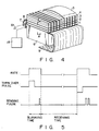
- Fig. 4 is a perspective view showing a schematic arrangement of an ultrasonic probe according to the second embodiment of the present invention.
- Acoustic matching layers 2, 3, and 4 and an acoustic lens 5 are formed on the ultrasonic radiation side of a stacked piezoelectric element 1, whereas a backing member 6 as a base of a probe head is formed on the rear surface side.
- the stacked piezoelectric element 1 is formed by stacking two piezoelectric layers on each other. An inner electrode is bonded to the interface between these piezoelectric layers, whereas outer electrodes are respectively bonded to both end faces of the element 1 in the stacking direction, i.e., one each of the upper and lower outer electrodes are formed.
- the acoustic matching layers 2, 3, and 4 and the acoustic lens 5 as upper members and the backing member 6 as a lower member are formed to sandwich the stacked piezoelectric layer, thus constituting a probe head having an integrated structure, as shown in Fig. 4.
- the thicknesses of the three matching layers 2, 3, and 4 are set to ensure matching on the high-frequency side. Such setting is performed to acquire a B mode signal on the high-frequency side and to broaden a sensitivity band.
- the stacked layers except for the acoustic lens 5 on the uppermost portion and the backing member 6 are formed into strips.
- a common ground electrode line is soldered to one outer electrode, and signal lines of a flexible print plate 9 are soldered to the other outer electrode. More specifically, the pitch of the signal lines of the flexible print plate 9 is set to be 0.15 mm, which is an optimal value calculated in relation to a cutting operation by a dicing machine using a 30-» thick blade used for forming the above-mentioned strips.
- a polarization reversing circuit 18 capable of turning over the polarity is used to supply power to the electrodes of this head.
- the circuit 18 includes a DC power supply connected to the stacked piezoelectric element through polarity turn over common electrode lines 7 and 8 between one outer electrode and the inner electrode of the stacked piezoelectric layer.
- the polarity of the DC power supply of the polarization reversing circuit 18 connected to the stacked piezoelectric element is manually or automatically reversed, the polarization directions of every two adjacent stacked layers can be changed to opposite directions regardless of whether the initial polarization directions of the adjacent piezoelectric layers are the same or opposite to each other. Therefore, no special consideration need be given to the initial polarization directions of the piezoelectric layers connected to the DC power supply.
- Fig. 5 is a timing chart of voltage pulses for driving the ultrasonic probe according to the present invention.
- a blanking time as a setting time of the system is 30 »s.
- a sending pulse is applied 10 »s after the end of this blanking time. Therefore, a polarization turn over operation has a margin of about 20 »s.
- a reversing pulse is applied only for 15 »s. Since this piezoelectric element has a coercive electric field of 1 kV/mm, a voltage of ⁇ 200 V is applied.
- the polarization reversing circuit is constituted by an FET switch.
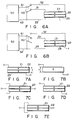
- FIGs. 6A and 6B are circuit diagrams, each showing a schematic connecting state of an ultrasonic probe according to the present invention.
- a piezoelectric vibrator 1 is constituted by a stacked layer (piezoelectric layer) formed by bonding two piezoelectric ceramic members, as piezoelectric elements having substantially the same thickness, to each other in the direction of thickness.
- Two different types of frequency bands are excited from the single vibrator 1 by controlling the polarities of driving pulses to be respectively applied to electrodes 21, 22, and 23 formed on the interfaces between the layers of this two-layer piezoelectric vibrator 1.
- a pulser/receiver circuit for processing reception signals of a driving pulse source and the vibrator has two terminals, i.e., a GND terminal 62 and a signal terminal 61.
- the three terminals of the vibrator 1 are connected to the two terminals of the pulser/receiver circuit through two switches, as shown in Figs. 6A and 6B. Since the resonance frequency of the vibrator 1 is changed by operating these switches, two types of frequencies can be excited. The principle of this operation will be described below with reference to Figs. 7A to 7E.
- Fig. 7A shows a piezoelectric vibrator of this embodiment.
- Fig. 7B shows a single-layer piezoelectric vibrator equivalent to the vibrator in Fig. 7A.
- a two-layered vibrator is designed such that the stacked layers have the same polarization direction, and a pulse is applied between electrodes 21 and 23 respectively formed on the upper and lower surfaces of the piezoelectric element.
- An inner electrode 22 is formed in an electrically floating state.
- the resonance frequency of the vibrator is determined by a total thickness t of the two-layered vibrator, and the thickness of each electrode can be substantially neglected as compared with the thickness of the ceramic layer, the thickness of the vibrator in Fig. 7B is equivalent to the thickness t .
- the resonance frequency and the electric impedance are respectively represented by f0 and Z0.
- Fig. 7C shows a modification in which a piezoelectric vibrator and electrodes are connected in a different manner. More specifically, Fig. 7C shows a piezoelectric element in which the two layers of a two-layered vibrator are stacked on each other to have opposite polarization directions. Electrodes 21 and 23 on the upper and lower surfaces of the element are commonly connected, and a pulse is applied between an inner electrode 22 and the electrodes 21 and 23. Similarly, in this case, electric field of a pulse is directed to the same direction as the polarization direction of each ceramic layer. Therefore, if the total thickness of the element is t , the resonance frequency is f0. However, the electric impedance between the two terminals is reduced to 1/4 that of the element shown in Figs. 7A and 7B. This is a low impedance effect due to the stacked structure.
- a pulse is applied between two surface electrodes 21 and 23.
- This arrangement is equivalent to a combination of a layer in which the directions of polarization and an electric field coincide with each other and a layer in which the directions of polarization and an electric field are opposite to each other (as disclosed in U.S.P. Application No. 13,891,075).
- the resonance frequency of the element shown in Fig. 7D is given by 2f0 which is twice that of the element shown in Fig. 7A, providing that they have the same thickness.
- the electric impedance of this element is given by Z0 which is the same as that of the element in Fig. 7A.
- Fig. 7E shows a structure constituted by a combination of a layer in which the directions of polarization and an electric field coincide with each other and a layer in which the directions of polarization and an electric field are opposite to each other.
- the resonance frequency is given by 2f0, similar to the element in Fig. 7D.
- the electric impedance is reduced to Z0/4, similar to the element shown in Fig. 7C. That is, the resonance frequency can be increased to a multiple of the number of layers, or the electric impedance can be reduce to 1/the square of the number of layers by a combination of the polarization direction of each layer of a multilayered structure and an electric field direction.
- the resonance states of the stacked layers shown in Figs. 7A to 7E can be selectively realized by a switching operation of a switch 40 shown in Figs. 6A and 6B.
- a switch 40 shown in Figs. 6A and 6B With the arrangement shown in Fig. 7A, an ultrasonic probe having the resonance frequency f0 and the electric impedance Z0 can be realized.
- Fig. 7B With the arrangement shown in Fig. 7B, an ultrasonic probe having the resonance frequency 2f0 and the electric impedance Z0/4 can be realized.
- Fig. 8 shows still another embodiment of the present invention.
- a stacked piezoelectric element is designed to be selectively switched to the resonance states of the stacked layers shown in Figs. 7C and 7D
- an ultrasonic probe system can be provided, in which two types of combinations of resonance frequencies and electric impedances, i.e., f0 and Z0/4, and 2f0 and Z0, can be selectively switched.
- f0 and Z0/4 i.e., f0 and Z0/4, and 2f0 and Z0
- the resulting structure can be driven in two types of frequency bands including frequencies having a frequency ratio of 2.
- this switch is preferably arranged on the probe side, it may be arranged on the side of the diagnosing apparatus main body.
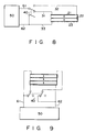
- Fig. 9 shows an ultrasonic probe using a vibrator having a three-layered structure, which can be driven in two types of frequency bands including frequencies having a frequency ratio of 3 (3f0) by operating a switch.
- ultrasonic waves having a plurality of different types of frequencies can be acquired through the same plane of the stacked electric member of one ultrasonic probe.
- desired frequencies in these frequency bands can be arbitrarily selected and used in accordance with application purposes.
- the present invention is not limited to the embodiment described above. Various changes and modifications can be made within the spirit and scope of the invention.
- the stacked piezoelectric member has the two-layered structure in this embodiment.
- a stacked piezoelectric element consisting of three or more layers may be used.
- a plurality of piezoelectric layers are stacked on each other such that the polarization directions of every two adjacent layers are opposite to each other or the polarization directions of all the layers coincide with each other.
- a DC power supply which can apply a voltage higher than the coercive electric field of the piezoelectric member, to one set of every other piezoelectric layers of a stacked piezoelectric element, in which electrodes are bonded to the two end faces in the stacking direction and the interface between the piezoelectric layers, can be connected to the element through a polarization reversing circuit capable of reversing the polarity within a blanking time of the system.
- an ultrasonic probe system which has an ultrasonic probe capable of selectively transmitting/receiving ultrasonic waves having two different types of frequencies through the same plane of a probe head, and capable of simultaneously acquiring a wide-band B mode signal in a high-frequency region, and a high-sensitivity Doppler signal in a low-frequency region.
Description
- The present invention relates to an ultrasonic probe used for an ultrasonic test apparatus and, more particularly, to an ultrasonic probe system which is constituted by a stacked piezoelectric element and is capable of transmitting/receiving ultrasonic waves having different frequencies.
- A detailed description of the prior art is available from the following references:
- (1) Japanese Patent Disclosure (Koukai) No. 60-41399
- (2) Japanese Patent Disclosure (Koukai) No. 61-69298
- An ultrasonic probe has a probe head mainly constituted by a piezoelectric element. This ultrasonic probe is used to obtain image data representing the internal state of a target object by radiating ultrasonic waves onto the target object and immediately receiving waves reflected from interfaces of the target object which have different acoustic impedances. An ultrasonic test apparatus using such an ultrasonic probe is used in practice as, e.g., a medical diagnosing apparatus for examining the inside of a human body, or an industrial test apparatus for inspecting flaws in welded metal portions.
- The diagnosing function of a medical diagnosing apparatus has been greatly improved owing to the development of "the color flow mapping (CFM) method" in addition to photography of a tomographic image (B mode image) of a human body. In this CFM method, blood flow rates in a heart, a liver, a carotid artery, and the like as targets are two-dimensionally displayed in color by using the Doppler effect. Recently, the CFM method has been used to diagnose all kinds of internal organs of a human body, such as the uterus, the kidney, and the pancreas. Further studies of the CFM method are now in progress to allow observation of even the movement of a coronary blood flow.
- With regard to the above-mentioned B mode image, i.e., a tomographic image of a human body, it is required that a high-resolution image be obtained with high sensitivity to allow an operator to clearly observe a physical change or a cavity as a slight morbid alteration. In the Doppler mode for acquiring a CFM image or the like, since echoes (waves) reflected by, e.g., microscopic blood cells, each having a diameter of several »m, are used, the resulting signal level is lower than that obtained in the B mode described above. For this reason, high-sensitivity performance is especially required. In many cases, a reference frequency in this Doppler mode is set to be lower than the center frequency in the frequency band of an ultrasonic probe. This is because a frequency component exhibiting small attenuation is used to suppress the influences, of ultrasonic attenuation through a living body, which cause a decrease in S/N ratio. Therefore, providing that ultrasonic waves having two different types of frequency components can be transmitted/received by a single ultrasonic probe, both a high-resolution B mode image constituted by high-frequency components and a high-sensitivity Doppler image constituted by low-frequency components can be obtained. As probes having such functions, "duplex type ultrasonic probes" are available from various manufacturers. A duplex type ultrasonic probe is designed such that two types of vibrators having different resonance frequencies are arranged in one ultrasonic probe. Since an ultrasonic probe of this type uses different types of vibrators, ultrasonic transmission/reception planes are set at different positions. For this reason, tomographic images of the same portion cannot be observed. Under the circumstances, a method of transmitting/receiving ultrasonic waves in two types of frequency bands by using a single vibrator has been proposed, which uses a stacked piezoelectric element disclosed in Japanese Patent Disclosure (Koukai) No. 60-41399. Two types of frequency bands can be separated from each other by using a combination of an ultrasonic probe of this type, a driving pulser, and a filter. As a result, a B mode signal and a Doppler signal can be respectively acquired from high-frequency components and low-frequency components. However, in the ultrasonic probe having the above-described arrangement, since the electromechanical coupling efficiency of one piezoelectric element is divided into substantially halves, the high-frequency side frequency band is narrowed, and the remaining time (duration) of an echo signal is prolonged. For this reason, even if a B mode image is obtained by using high-frequency components to ensure high resolution, the resulting resolution is not so high as expected. That is, there is a room for improvement in this point. In addition, since low-frequency components are generally decreased in number as the frequency band becomes narrower, the S/N ratio is decreased, resulting in insufficient penetration. This is because an echo signal reflected by a portion located deep in a living body is mainly constituted by frequency components lower than the center frequency of transmitted ultrasonic waves. The specific band width of frequency components, which is required to obtain a good B mode image, is 40% or more of its center frequency. Assume that a single-layered piezoelectric element is used. In this case, a specific band width with respect to a center frequency at -6 dB is 40 to 50% in one-layer matching, and 60 to 70% in two-layer matching. In contrast to this, if the stacked piezoelectric element having the above-described arrangement is used, specific band widths of 25% and 35% are respectively set in one-layer matching and two-layer matching. That is, if only the stacked piezoelectric element is used, the obtained specific band width is only about 1/2 that obtained when the single-layered piezoelectric element is used.
- An increase in sensitivity may be realized by increasing a driving voltage. This method, however, is also limited by the problem of heat generated by a piezoelectric element. Another problem posed in the method of obtaining two types of frequency bands by using a single ultrasonic probe is that the same portion cannot be observed because of the use of a plurality of vibrators having different resonance frequencies. As described above, in order to solve this problem, the stacked piezoelectric element is disclosed in Japanese Patent Disclosure (Koukai) No. 60-41399, which is obtained by stacking piezoelectric elements, each having substantially the same thickness as that of the single-layered piezoelectric element and consisting of substantially the same material as therefor. This element, however, poses the problem of a narrow specific band of high-frequency components.
- As described above, when ultrasonic waves in two types of frequency bands are to be acquired by one ultrasonic probe, the same portion of a target object cannot be observed with a probe head constituted by a plurality of vibrators having different resonance frequencies. In the stacked piezoelectric element disclosed in Japanese Patent Disclosure (Koukai) No. 60-41399 to solve this problem, which is obtained by stacking layers, each having substantially the same thickness as that of the single-layered piezoelectric element and consisting of substantially the same material as therefor, the specific band of high-frequency components is too narrow.
- GB-A-2083695 discloses an ultrasonic transducer having a plurality of piezoelectric body layers laminated one on another with electrode layers on opposite faces thereof. The piezoelectric body layers have their electrodes wired to an oscillator such that they oscillate in the same thickness vibration mode. At least one of such electrode wirings has a change-over switch connected in circuit thereto. A switching operation of the switch will change the number of piezoelectric body layers set into oscillation and thus will cause the cumulative thickness of the effective oscillating piezoelectric body layers to be changed in order to vary the resonance frequency of the transducer.
- It is an object of the present invention to provide an ultrasonic probe system including an ultrasonic probe which easily allows an increase in transmission frequency without posing problems in terms of manufacture and characteristics.
- It is another object of the present invention to provide an ultrasonic probe system which allows an increase in sensitivity of reception performance in addition to an increase in transmission frequency, can transmit/receive two types of ultrasonic waves through the same plane of a probe, and has frequency characteristics exhibiting a sufficiently large band width of high-frequency components.
- According to the present invention, there is provided an ultrasonic probe system comprising probe head means, said probe head means comprising: a stacked piezoelectric element including a plurality of piezoelectric layers stacked on each other in a direction of thickness, a plurality of first electrodes in contact with two end faces of said plurality of piezoelectric layers in a stacking direction, and at least one second electrode in contact with an interface between said plurality of piezoelectric layers; ultrasonic focusing means in contact with an upper surface of ultrasonic frequency matching means and having a convex surface directed outwardly; wiring means connected to said first electrode of said piezoelectric layer; and said probe system comprising control means for controlling said ultrasonic frequency and thereby controlling polarization directions of said plurality of piezoelectric layers, characterized in that a DC power supply capable of applying a voltage higher than a coercive electric field of each of said piezoelectric layers is connected to one first electrode and the or at least one second electrode and in that said system further comprises polarization reversing circuit means for, when said DC power supply is energized, reversing the polarity of said DC power supply so as to direct electric fields of every two adjacent layers constituting said piezoelectric layers in substantially opposite directions or electric fields of all the layers in the same direction, thereby selectively generating ultrasonic waves having a plurality of different frequencies.
- In one arrangement according to the invention, there are provided ground means connected to one of said first electrodes or said second electrode.
- Preferably, the system comprises ultrasonic frequency matching means constituted by a plurality of layers bonded to one surface of said stacked piezoelectric element and head base means bonded to the other surface of said stacked piezoelectric element and the system is characterized in that one of said first electrodes is an outer electrode connected to said wiring means, said second electrode is an inner electrode connected to said polarization reversing circuit means, said ultrasonic frequency matching means is an acoustic matching layer, said ultrasonic focusing means is an acoustic lens, said head base means is a backing member, said ground means is a ground plate connected to one of said first electrodes, and said wiring means is a flexible print board on which a print wiring pattern connected to said piezoelectric layer is formed.
- In the ultrasonic probe of the present invention, since a DC power supply capable of manually or automatically reversing its polarity is connected to the stacked piezoelectric element, when the voltage higher than the coercive electric field is applied to one set of every other stacked piezoelectric layers, the minimum (fundamental) resonance frequency differs depending on whether the polarization directions of one set of every other piezoelectric layers to which the DC power supply is connected coincide or are opposite to those of the other set of every other piezoelectric layers to which the DC power supply is not connected. If the thickness of each piezoelectric layer is represented by t, the number of layers is represented by n, and the sound velocity of the piezoelectric member is represented by v, a fundamental resonance frequency f0, when all the polarization directions coincide with each other, satisfies the following equation:

In contrast to this, if the polarization directions of every two adjacent piezoelectric layers are opposite to each other, the following equation is established:

Such equations are established for the following reasons. If the polarization directions coincide with each other, the stacked piezoelectric element is equivalent to a one-layer piezoelectric element having a thickness nt. This means 1/2-wavelength resonance occurs in such a manner that the two end faces serve as loops of vibrations, and the middle point in the direction of thickness serves as a node. In contrast to this, assume that the polarization directions of every two adjacent piezoelectric layers are opposite to each other. In this case, when an arbitrary piezoelectric layer extends, an adjacent piezoelectric layer contracts. Therefore, n/2-wavelength resonance occurs in such a manner that the two end faces of the piezoelectric element in the direction of thickness serve as loops of vibrations, and the middle point serves as a node. Therefore, the resulting resonance frequency is n times that obtained when the polarization directions coincide with each other. - Preferably this resonance frequency Conversion is performed by supplying a polarization reversing pulse and a sending pulse generated by a pulser constituted by this ultrasonic probe system, and a "reversing " operation is performed within a blanking time, of a so-called system operating time, immediately before the reception mode of the system. This "blanking time" is a setting time of the system, during which data transmission and the like are performed. Although the blanking time varies depending on the type of an ultrasonic probe or a diagnosing apparatus, it is normally set to be 20 to 40 »s (see Fig. 5). Since a sending pulse is supplied to the ultrasonic probe within 10 »s after the end of this blanking time, the duration of time in which no transmission/reception of ultrasonic waves is performed (actual blanking time) is 10 to 30 »s. Since the polarization of each piezoelectric layer can be reversed by applying the voltage higher than the coercive electric field for several »s, this operation can be performed within 10 to 30 »s, for which no transmission/reception is performed. As a result, since the frequencies of sending ultrasonic waves can be switched at the same timing as that in a conventional diagnosing apparatus, a high-resolution, high-frequency B mode signal and a high-sensitivity, low-frequency Doppler signal can be acquired at the same timing as that in the conventional diagnosing apparatus. Therefore, a B mode image constituted by this high-frequency wave and a CFM image constituted by this low-frequency wave can be obtained in real time.
- This invention can be more fully understood from the following detailed description when taken in conjunction with the accompanying drawings, in which:
- Fig. 1 is a perspective view showing a schematic arrangement of an ultrasonic probe according to the first embodiment of the present invention;
- Figs. 2A and 2B are enlarged sectional views, of a stacked piezoelectric element in Fig. 1, taken along a line A - A';
- Fig. 3A is graph showing the frequency spectrum of an echo wave measured by the "pulse echo method" when every two adjacent piezoelectric layers have opposite polarization directions;
- Fig. 3B is a graph showing a frequency spectrum measured by the "pulse echo method" when every two adjacent piezoelectric layers have the same polarization direction;
- Fig. 4 is a perspective view showing a schematic arrangement of an ultrasonic probe according to the second embodiment of the present invention;
- Fig. 5 is a timing chart of various types of pulses for driving the ultrasonic probe;
- Figs. 6A and 6B are circuit diagrams, each showing a schematic connecting state of a polarization reversing circuit of the ultrasonic probe according to the present invention;
- Fig. 7A is a wiring diagram showing a piezoelectric layer having a two-layered structure;
- Fig. 7B is a wiring diagram showing a piezoelectric layer having a one-layered structure;
- Figs. 7C to 7E are wiring diagrams, each showing the polarization direction of each layer of the two-layered piezoelectric element;
- Fig. 8 is a schematic wiring diagram showing an ultrasonic probe system according to another embodiment of the ultrasonic probe shown in Figs. 6A and 6B; and
- Fig. 9 is a schematic wiring diagram showing an ultrasonic probe system including a stacked piezoelectric element constituted by three layers according to still another embodiment of the present invention.
- In an ultrasonic probe system according to the first embodiment of the present invention shown in Fig. 1, acoustic matching layers 2, 3, and 4 and an
acoustic lens 5 are formed on the ultrasonic radiation side of a stacked piezoelectric element 1, while abacking member 6 as a base of a probe head is formed on the rear surface side. The stacked piezoelectric element 1 is formed by stacking two piezoelectric layers on each other. An inner electrode is bonded to the interface between these piezoelectric layers, whereas outer electrodes are respectively bonded to both end faces of the element 1 in the stacking direction, i.e., one each of the upper and lower outer electrodes are formed. The acoustic matching layers 2, 3, and 4 and theacoustic lens 5 are formed on the piezoelectric layer, and thebacking member 6 is formed under the piezoelectric layer. With this arrangement, the piezoelectric layer is sandwiched between these upper and lower members, thus constituting a probe head having an illustrated integrated structure. - The thicknesses of the three matching layers 2, 3, and 4 are set to ensure matching on the high-frequency side. Such setting is performed to acquire a B mode signal on the high-frequency side and to broaden a sensitivity band.
- In this ultrasonic probe, the stacked layers except for the
acoustic lens 5 on the uppermost portion and thebacking member 6 are formed into strips. A common ground electrode line (not shown) is soldered to one outer electrode, and signal lines of a flexible print plate 9 are soldered to the other outer electrode. More specifically, the pitch of the signal lines of the flexible print plate 9 is set to be 0.15 mm, which is an optimal value calculated in relation to a cutting operation by a dicing machine using a 30-» thick blade used for forming the above-mentioned strips. - A
DC power supply 18 capable of reversing its polarity is connected to the stacked piezoelectric element through polarity reversalcommon electrode lines DC power supply 18 connected to the stacked piezoelectric element is manually or automatically reversed, the polarization directions of every two adjacent stacked layers can be changed to substantially opposite directions regardless of whether the initial polarization directions of the adjacent piezoelectric layers are the same or opposite to each other. Therefore no special consideration need be given to the initial polarization directions of the piezoelectric layers connected to theDC power supply 18 capable of reversing polarity. - Figs. 2A and 2B are enlarged sectional views, of the stacked piezoelectric element in Fig. 1, taken along a line A - A'. As shown in Fig. 2A, in this stacked piezoelectric element for example, two piezoelectric layers 11 and 12 are stacked on each other such that polarization directions (arrows) 13 and 14 oppose each other in an initial state.
Outer electrodes inner electrode 17 is bonded to the interface between the piezoelectric layers 11 and 12. In the embodiment shown in Fig. 2A, the adjacent two piezoelectric layers have opposite polarization directions. However, the initial polarization directions of the piezoelectric layers of a stacked piezoelectric element may have same polarization direction, as polarization directions 13' and 14' in Fig. 2B, as long as the piezoelectric layers are connected to the above-mentioned DC power supply capable of reversing polarity. - Each of the piezoelectric layers 11 and 12 is composed of a piezoelectric ceramic material, called a PZT ceramic material having a specific permittivity of 2,000, to have a thickness of 200 »m. The cross sections of the stacked piezoelectric element 1 constituting this probe head are arranged in an array of strips, as shown in Figs. 2A and 2B. In the manufacture of the probe head, therefore, the stacked piezoelectric element including matching layers (not shown), which are bonded to the upper surface, is cut in the stacking direction (i.e., vertical direction) by a dicing machine using a blade. Thereafter, the cut portions are horizontally arranged at a predetermined pitch. In this case, the pitch is set to be 0.15 mm.
- Fig. 3A is a graph showing the frequency spectrum of an echo wave reflected by a reflector in water and measured by the "pulse echo method". According to this graph, a center frequency is about 7 MHz (an actual measurement value: 7.54 MHz), and a specific band of -6 dB corresponds to 52.9% of the center frequency. It is apparent from the values indicated by the graph that a frequency band wide enough to obtain a good B mode image by using an ultrasonic imaging apparatus using an ultrasonic probe can be obtained.
- Fig. 3B is a graph showing the frequency spectrum of an echo wave measured by the "pulse echo method", more specifically, a characteristic curve obtained when the polarization direction of a given piezoelectric layer is reversed by applying a DC voltage of 400 V to the layer for about 10 seconds by using a DC power supply capable of reversing polarity so that the polarization directions of all the piezoelectric layers are set to be the same. As indicated by this graph, a center frequency of about 3.5 MHz (an actual measurement value: 3.71 MHz) is set, and a specific band of -6 dB corresponds to 51.9% of the center frequency.
- When all the polarization directions are changed to the same direction by using this DC power supply, the center frequency of an echo wave is reduced to about 1/2. If a voltage having the opposite polarity is applied to a corresponding piezoelectric layer in this state, the polarization directions are restored to the initial state in this embodiment, i.e., the opposite directions.
- As is apparent from the above experimental results, two different types of ultrasonic waves can be acquired by the same plane of one ultrasonic probe.
- The present invention is not limited to the embodiment described above. Various changes and modifications can be made within the spirit and scope of the invention. For example, in this embodiment, the two-layered stacked piezoelectric element is used. However, a stacked piezoelectric constituted by three or more layers may be used.
- According to the first embodiment of the present invention, a plurality of piezoelectric layers are stacked on each other such that the polarization directions of every two adjacent layers are opposite to each other or the polarization directions of all the layers are the same, and a DC power supply capable of reversing the polarity by applying a voltage higher than the coercive electric field of a piezoelectric member to one set of every other layers of a stacked piezoelectric element in which electrodes are bonded to the two end faces in the stacking direction and the interface between the piezoelectric layers can be connected to the element. With this arrangement, the polarization directions of the respective piezoelectric layers of the stacked piezoelectric element can be set to substantially desired directions, thereby realizing an ultrasonic probe system which can be used without limitation in terms of the initial polarization directions of piezoelectric layers. In addition, an ultrasonic probe system can be provided, which can transmit/receive ultrasonic waves having two different types of frequencies through the same plane of a probe head of an ultrasonic probe, and can simultaneously acquire a wideband B mode signal in a high-frequency region and a high-sensitivity Doppler signal in a low-frequency region.
- Fig. 4 is a perspective view showing a schematic arrangement of an ultrasonic probe according to the second embodiment of the present invention. Acoustic matching layers 2, 3, and 4 and an
acoustic lens 5 are formed on the ultrasonic radiation side of a stacked piezoelectric element 1, whereas abacking member 6 as a base of a probe head is formed on the rear surface side. The stacked piezoelectric element 1 is formed by stacking two piezoelectric layers on each other. An inner electrode is bonded to the interface between these piezoelectric layers, whereas outer electrodes are respectively bonded to both end faces of the element 1 in the stacking direction, i.e., one each of the upper and lower outer electrodes are formed. The acoustic matching layers 2, 3, and 4 and theacoustic lens 5 as upper members and thebacking member 6 as a lower member are formed to sandwich the stacked piezoelectric layer, thus constituting a probe head having an integrated structure, as shown in Fig. 4. - The thicknesses of the three matching layers 2, 3, and 4 are set to ensure matching on the high-frequency side. Such setting is performed to acquire a B mode signal on the high-frequency side and to broaden a sensitivity band.
- In this ultrasonic probe, the stacked layers except for the
acoustic lens 5 on the uppermost portion and thebacking member 6 are formed into strips. A common ground electrode line is soldered to one outer electrode, and signal lines of a flexible print plate 9 are soldered to the other outer electrode. More specifically, the pitch of the signal lines of the flexible print plate 9 is set to be 0.15 mm, which is an optimal value calculated in relation to a cutting operation by a dicing machine using a 30-» thick blade used for forming the above-mentioned strips. - A
polarization reversing circuit 18 capable of turning over the polarity is used to supply power to the electrodes of this head. Thecircuit 18 includes a DC power supply connected to the stacked piezoelectric element through polarity turn overcommon electrode lines polarization reversing circuit 18 connected to the stacked piezoelectric element is manually or automatically reversed, the polarization directions of every two adjacent stacked layers can be changed to opposite directions regardless of whether the initial polarization directions of the adjacent piezoelectric layers are the same or opposite to each other. Therefore, no special consideration need be given to the initial polarization directions of the piezoelectric layers connected to the DC power supply. - Fig. 5 is a timing chart of voltage pulses for driving the ultrasonic probe according to the present invention. A blanking time as a setting time of the system is 30 »s. A sending pulse is applied 10 »s after the end of this blanking time. Therefore, a polarization turn over operation has a margin of about 20 »s. In this embodiment, a reversing pulse is applied only for 15 »s. Since this piezoelectric element has a coercive electric field of 1 kV/mm, a voltage of ∓200 V is applied. Note that the polarization reversing circuit is constituted by an FET switch.
- Figs. 6A and 6B are circuit diagrams, each showing a schematic connecting state of an ultrasonic probe according to the present invention. A piezoelectric vibrator 1 is constituted by a stacked layer (piezoelectric layer) formed by bonding two piezoelectric ceramic members, as piezoelectric elements having substantially the same thickness, to each other in the direction of thickness. Two different types of frequency bands are excited from the single vibrator 1 by controlling the polarities of driving pulses to be respectively applied to
electrodes electrodes GND terminal 62 and asignal terminal 61. The three terminals of the vibrator 1 are connected to the two terminals of the pulser/receiver circuit through two switches, as shown in Figs. 6A and 6B. Since the resonance frequency of the vibrator 1 is changed by operating these switches, two types of frequencies can be excited. The principle of this operation will be described below with reference to Figs. 7A to 7E. - Fig. 7A shows a piezoelectric vibrator of this embodiment. Fig. 7B shows a single-layer piezoelectric vibrator equivalent to the vibrator in Fig. 7A. Referring to Fig. 7A, a two-layered vibrator is designed such that the stacked layers have the same polarization direction, and a pulse is applied between
electrodes inner electrode 22 is formed in an electrically floating state. In this case, since the resonance frequency of the vibrator is determined by a total thickness t of the two-layered vibrator, and the thickness of each electrode can be substantially neglected as compared with the thickness of the ceramic layer, the thickness of the vibrator in Fig. 7B is equivalent to the thickness t. Assume, in this case, that the resonance frequency and the electric impedance are respectively represented by f0 and Z0. - Fig. 7C shows a modification in which a piezoelectric vibrator and electrodes are connected in a different manner. More specifically, Fig. 7C shows a piezoelectric element in which the two layers of a two-layered vibrator are stacked on each other to have opposite polarization directions.
Electrodes inner electrode 22 and theelectrodes - In the connecting structure shown in Fig. 7D as a modification, although stacked layers have opposite polarization directions, a pulse is applied between two
surface electrodes - Fig. 7E shows a structure constituted by a combination of a layer in which the directions of polarization and an electric field coincide with each other and a layer in which the directions of polarization and an electric field are opposite to each other. In this case, therefore, the resonance frequency is given by 2f0, similar to the element in Fig. 7D. In addition, the electric impedance is reduced to Z0/4, similar to the element shown in Fig. 7C. That is, the resonance frequency can be increased to a multiple of the number of layers, or the electric impedance can be reduce to 1/the square of the number of layers by a combination of the polarization direction of each layer of a multilayered structure and an electric field direction.
- With the arrangement described above, the resonance states of the stacked layers shown in Figs. 7A to 7E can be selectively realized by a switching operation of a
switch 40 shown in Figs. 6A and 6B. With the arrangement shown in Fig. 7A, an ultrasonic probe having the resonance frequency f0 and the electric impedance Z0 can be realized. With the arrangement shown in Fig. 7B, an ultrasonic probe having the resonance frequency 2f0 and the electric impedance Z0/4 can be realized. - Fig. 8 shows still another embodiment of the present invention. If a stacked piezoelectric element is designed to be selectively switched to the resonance states of the stacked layers shown in Figs. 7C and 7D, an ultrasonic probe system can be provided, in which two types of combinations of resonance frequencies and electric impedances, i.e., f0 and Z0/4, and 2f0 and Z0, can be selectively switched. As described above, if a two-layered vibrator consisting of two identical layers is formed into a three-terminal structure, and the application conditions of driving pulses are selectively switched, the resulting structure can be driven in two types of frequency bands including frequencies having a frequency ratio of 2. Although this switch is preferably arranged on the probe side, it may be arranged on the side of the diagnosing apparatus main body.
- Fig. 9 shows an ultrasonic probe using a vibrator having a three-layered structure, which can be driven in two types of frequency bands including frequencies having a frequency ratio of 3 (3f0) by operating a switch.
- As is apparent from the above description, by switching combinations of layers constituting a piezoelectric element and their polarities in accordance with a predetermined combination, ultrasonic waves having a plurality of different types of frequencies (two types in this embodiment) can be acquired through the same plane of the stacked electric member of one ultrasonic probe. In diagnosis, therefore, desired frequencies in these frequency bands can be arbitrarily selected and used in accordance with application purposes.
- The present invention is not limited to the embodiment described above. Various changes and modifications can be made within the spirit and scope of the invention. For example, the stacked piezoelectric member has the two-layered structure in this embodiment. However, a stacked piezoelectric element consisting of three or more layers may be used.
- According to the second embodiment of the present invention, a plurality of piezoelectric layers are stacked on each other such that the polarization directions of every two adjacent layers are opposite to each other or the polarization directions of all the layers coincide with each other. In addition, a DC power supply, which can apply a voltage higher than the coercive electric field of the piezoelectric member, to one set of every other piezoelectric layers of a stacked piezoelectric element, in which electrodes are bonded to the two end faces in the stacking direction and the interface between the piezoelectric layers, can be connected to the element through a polarization reversing circuit capable of reversing the polarity within a blanking time of the system. With this arrangement, the polarization direction of each piezoelectric layer of the stacked piezoelectric element can be set to a substantially desired direction, thereby realizing an ultrasonic probe system which can be used without being limited by the original polarization directions of the piezoelectric layers. In addition, an ultrasonic probe system can be provided, which has an ultrasonic probe capable of selectively transmitting/receiving ultrasonic waves having two different types of frequencies through the same plane of a probe head, and capable of simultaneously acquiring a wide-band B mode signal in a high-frequency region, and a high-sensitivity Doppler signal in a low-frequency region.
Claims (4)
- An ultrasonic probe system comprising probe head means (10),
said probe head means comprising:
a stacked piezoelectric element (1) including a plurality of piezoelectric layers (11,12) stacked on each other in a direction of thickness, a plurality of first electrodes (15,16) in contact with two end faces of said plurality of piezoelectric layers in a stacking direction, and at least one second electrode (17) in contact with an interface between said plurality of piezoelectric layers;
ultrasonic focusing means (5) in contact with an upper surface of ultrasonic frequency matching means and having a convex surface directed outwardly;
wiring means (9) connected to said first electrode (16) of said piezoelectric layer (12); and
said probe system comprising control means (18) for controlling said ultrasonic frequency and thereby controlling polarization directions of said plurality of piezoelectric layers (11,12),
characterized in that a DC power supply capable of applying a voltage higher than a coercive electric field of each of said piezoelectric layers is connected to one first electrode and the or at least one second electrode and in that said system further comprises polarization reversing circuit means (18) for, when said DC power supply is energized, reversing the polarity of said DC power supply so as to direct electric fields of every two adjacent layers constituting said piezoelectric layers in substantially opposite directions or electric fields of all the layers in the same direction, thereby selectively generating ultrasonic waves having a plurality of different frequencies. - A system according to claim 1, characterized in that when said polarization reversing circuit means (18) reverses the polarity of a voltage to be applied to direct electric fields of every two adjacent layers of said piezoelectric layers in substantially opposite directions or electric fields of all the layers in the same direction, said polarization reversing circuit means (18) performs control to apply the voltage during a blanking time of an operating time of said system, thereby performing conversion of a resonance frequency.
- A system according to claim 1, characterized by further comprising ground means (81) connected to one of said first electrodes (15,16) or said second electrode (17).
- A system according to claim 3, characterized by further comprising ultrasonic frequency matching means (2,3,4) constituted by a plurality of layers in contact with one surface of said stacked piezoelectric element, by comprising head base means (6) bonded to the other surface of said stacked piezoelectric element, and in that one of said first electrodes (15,16) is an outer electrode connected to said wiring means (9),
said second electrode (17) is an inner electrode connected to said polarization reversing circuit means (18),
said ultrasonic frequency matching means (2,3,4) is an acoustic matching layer,
said ultrasonic focusing means (5) is an acoustic lens,
said head base means (6) is a backing member,
said ground means is a ground plate connected to one of said first electrodes (15,16), and
said wiring means (9) is a flexible print board on which a print wiring pattern connected to said piezoelectric layer (12) is formed.
Applications Claiming Priority (2)
| Application Number | Priority Date | Filing Date | Title |
|---|---|---|---|
| JP7661790 | 1990-03-28 | ||
| JP76617/90 | 1990-03-28 |
Publications (3)
| Publication Number | Publication Date |
|---|---|
| EP0451984A2 EP0451984A2 (en) | 1991-10-16 |
| EP0451984A3 EP0451984A3 (en) | 1992-07-22 |
| EP0451984B1 true EP0451984B1 (en) | 1995-05-24 |
Family
ID=13610313
Family Applications (1)
| Application Number | Title | Priority Date | Filing Date |
|---|---|---|---|
| EP91302583A Expired - Lifetime EP0451984B1 (en) | 1990-03-28 | 1991-03-25 | Ultrasonic probe system |
Country Status (4)
| Country | Link |
|---|---|
| US (1) | US5163436A (en) |
| EP (1) | EP0451984B1 (en) |
| JP (1) | JP3015481B2 (en) |
| DE (1) | DE69109923T2 (en) |
Cited By (2)
| Publication number | Priority date | Publication date | Assignee | Title |
|---|---|---|---|---|
| DE19635593C1 (en) * | 1996-09-02 | 1998-04-23 | Siemens Ag | Ultrasound transducer for diagnostic and therapeutic use |
| DE19928765A1 (en) * | 1999-06-23 | 2001-01-11 | Siemens Ag | Ultrasonic transducer for multi-frequency, multi-layer test head can transmit different frequencies and receive frequency selectively over wide band with higher sensitivity than conventional arrangements |
Families Citing this family (125)
| Publication number | Priority date | Publication date | Assignee | Title |
|---|---|---|---|---|
| DE4139024C1 (en) * | 1991-11-27 | 1993-04-15 | Siemens Ag, 8000 Muenchen, De | |
| US5666953A (en) * | 1993-01-10 | 1997-09-16 | Wilk; Peter J. | System and associated method for providing information for use in forming medical diagnosis |
| US7497828B1 (en) | 1992-01-10 | 2009-03-03 | Wilk Ultrasound Of Canada, Inc. | Ultrasonic medical device and associated method |
| US5871446A (en) * | 1992-01-10 | 1999-02-16 | Wilk; Peter J. | Ultrasonic medical system and associated method |
| US6023632A (en) | 1997-07-16 | 2000-02-08 | Wilk; Peter J. | Ultrasonic medical system and associated method |
| US5744898A (en) * | 1992-05-14 | 1998-04-28 | Duke University | Ultrasound transducer array with transmitter/receiver integrated circuitry |
| US5410205A (en) * | 1993-02-11 | 1995-04-25 | Hewlett-Packard Company | Ultrasonic transducer having two or more resonance frequencies |
| US5381385A (en) * | 1993-08-04 | 1995-01-10 | Hewlett-Packard Company | Electrical interconnect for multilayer transducer elements of a two-dimensional transducer array |
| US5792058A (en) * | 1993-09-07 | 1998-08-11 | Acuson Corporation | Broadband phased array transducer with wide bandwidth, high sensitivity and reduced cross-talk and method for manufacture thereof |
| CA2139151A1 (en) * | 1994-01-14 | 1995-07-15 | Amin M. Hanafy | Two-dimensional acoustic array and method for the manufacture thereof |
| FR2722358B1 (en) * | 1994-07-08 | 1996-08-14 | Thomson Csf | BROADBAND MULTI-FREQUENCY ACOUSTIC TRANSDUCER |
| US5724976A (en) * | 1994-12-28 | 1998-03-10 | Kabushiki Kaisha Toshiba | Ultrasound imaging preferable to ultrasound contrast echography |
| JP3405840B2 (en) * | 1995-01-09 | 2003-05-12 | 株式会社東芝 | Ultrasonic probe and ultrasonic diagnostic apparatus using the same |
| US5834687A (en) * | 1995-06-07 | 1998-11-10 | Acuson Corporation | Coupling of acoustic window and lens for medical ultrasound transducers |
| US5655538A (en) | 1995-06-19 | 1997-08-12 | General Electric Company | Ultrasonic phased array transducer with an ultralow impedance backfill and a method for making |
| US5638822A (en) * | 1995-06-30 | 1997-06-17 | Hewlett-Packard Company | Hybrid piezoelectric for ultrasonic probes |
| US5657295A (en) * | 1995-11-29 | 1997-08-12 | Acuson Corporation | Ultrasonic transducer with adjustable elevational aperture and methods for using same |
| DE19609443C1 (en) * | 1996-03-11 | 1997-05-22 | Siemens Ag | Ultrasound converter e.g. for non-destructive testing |
| US5757727A (en) * | 1996-04-24 | 1998-05-26 | Acuson Corporation | Two-dimensional acoustic array and method for the manufacture thereof |
| US5957851A (en) * | 1996-06-10 | 1999-09-28 | Acuson Corporation | Extended bandwidth ultrasonic transducer |
| DE19733233C1 (en) * | 1997-08-01 | 1998-09-17 | Wolf Gmbh Richard | Electroacoustic transducer |
| US6319201B1 (en) | 1997-10-15 | 2001-11-20 | Peter J. Wilk | Imaging device and associated method |
| US6723063B1 (en) | 1998-06-29 | 2004-04-20 | Ekos Corporation | Sheath for use with an ultrasound element |
| US6582392B1 (en) | 1998-05-01 | 2003-06-24 | Ekos Corporation | Ultrasound assembly for use with a catheter |
| US5920972A (en) * | 1997-06-27 | 1999-07-13 | Siemens Medical Systems, Inc. | Interconnection method for a multilayer transducer array |
| US6049159A (en) * | 1997-10-06 | 2000-04-11 | Albatros Technologies, Inc. | Wideband acoustic transducer |
| US6050943A (en) | 1997-10-14 | 2000-04-18 | Guided Therapy Systems, Inc. | Imaging, therapy, and temperature monitoring ultrasonic system |
| US6541896B1 (en) * | 1997-12-29 | 2003-04-01 | General Electric Company | Method for manufacturing combined acoustic backing and interconnect module for ultrasonic array |
| US6121718A (en) * | 1998-03-31 | 2000-09-19 | Acuson Corporation | Multilayer transducer assembly and the method for the manufacture thereof |
| US6106463A (en) * | 1998-04-20 | 2000-08-22 | Wilk; Peter J. | Medical imaging device and associated method including flexible display |
| US6416478B1 (en) | 1998-05-05 | 2002-07-09 | Acuson Corporation | Extended bandwidth ultrasonic transducer and method |
| US6057632A (en) * | 1998-06-09 | 2000-05-02 | Acuson Corporation | Frequency and bandwidth controlled ultrasound transducer |
| US6320300B1 (en) * | 1998-09-03 | 2001-11-20 | Lucent Technologies Inc. | Piezoelectric array devices |
| US6007490A (en) * | 1998-11-25 | 1999-12-28 | Atl Ultrasound, Inc. | Ultrasonic probe with disconnectable transducer |
| US6552471B1 (en) * | 1999-01-28 | 2003-04-22 | Parallel Design, Inc. | Multi-piezoelectric layer ultrasonic transducer for medical imaging |
| US6139499A (en) * | 1999-02-22 | 2000-10-31 | Wilk; Peter J. | Ultrasonic medical system and associated method |
| US7288069B2 (en) * | 2000-02-07 | 2007-10-30 | Kabushiki Kaisha Toshiba | Ultrasonic probe and method of manufacturing the same |
| US6409667B1 (en) * | 2000-02-23 | 2002-06-25 | Acuson Corporation | Medical diagnostic ultrasound transducer system and method for harmonic imaging |
| US6517484B1 (en) | 2000-02-28 | 2003-02-11 | Wilk Patent Development Corporation | Ultrasonic imaging system and associated method |
| CA2332158C (en) * | 2000-03-07 | 2004-09-14 | Matsushita Electric Industrial Co., Ltd. | Ultrasonic probe |
| US6822374B1 (en) * | 2000-11-15 | 2004-11-23 | General Electric Company | Multilayer piezoelectric structure with uniform electric field |
| US6596239B2 (en) | 2000-12-12 | 2003-07-22 | Edc Biosystems, Inc. | Acoustically mediated fluid transfer methods and uses thereof |
| US7914453B2 (en) | 2000-12-28 | 2011-03-29 | Ardent Sound, Inc. | Visual imaging system for ultrasonic probe |
| EP1396172A2 (en) * | 2001-01-05 | 2004-03-10 | ANGELSEN, Bjorn A. J. | Wideband transducer |
| WO2002056666A2 (en) * | 2001-01-19 | 2002-07-25 | Angelsen Bjoern A J | A method of detecting ultrasound contrast agent in soft tissue, and quantitating blood perfusion through regions of tissue |
| US6429574B1 (en) | 2001-02-28 | 2002-08-06 | Acuson Corporation | Transducer array using multi-layered elements having an even number of elements and a method of manufacture thereof |
| US6664717B1 (en) | 2001-02-28 | 2003-12-16 | Acuson Corporation | Multi-dimensional transducer array and method with air separation |
| US6761688B1 (en) | 2001-02-28 | 2004-07-13 | Siemens Medical Solutions Usa, Inc. | Multi-layered transducer array and method having identical layers |
| US7344501B1 (en) * | 2001-02-28 | 2008-03-18 | Siemens Medical Solutions Usa, Inc. | Multi-layered transducer array and method for bonding and isolating |
| US6437487B1 (en) | 2001-02-28 | 2002-08-20 | Acuson Corporation | Transducer array using multi-layered elements and a method of manufacture thereof |
| DE60225795T2 (en) * | 2001-04-25 | 2009-04-16 | Philips Intellectual Property & Standards Gmbh | ARRANGEMENT WITH TWO PIEZOELECTRIC LAYERS AND METHOD FOR OPERATING A FILTER EQUIPMENT |
| JP3914002B2 (en) * | 2001-04-26 | 2007-05-16 | 日本電波工業株式会社 | Ultrasonic probe |
| WO2003017720A1 (en) * | 2001-08-16 | 2003-02-27 | Tayca Corporation | Multilayer piezoelectric oscillator |
| US6540683B1 (en) | 2001-09-14 | 2003-04-01 | Gregory Sharat Lin | Dual-frequency ultrasonic array transducer and method of harmonic imaging |
| US6976639B2 (en) | 2001-10-29 | 2005-12-20 | Edc Biosystems, Inc. | Apparatus and method for droplet steering |
| US6925856B1 (en) | 2001-11-07 | 2005-08-09 | Edc Biosystems, Inc. | Non-contact techniques for measuring viscosity and surface tension information of a liquid |
| AU2002359576A1 (en) | 2001-12-03 | 2003-06-17 | Ekos Corporation | Catheter with multiple ultrasound radiating members |
| US7285094B2 (en) | 2002-01-30 | 2007-10-23 | Nohara Timothy J | 3D ultrasonic imaging apparatus and method |
| US8226629B1 (en) | 2002-04-01 | 2012-07-24 | Ekos Corporation | Ultrasonic catheter power control |
| US7396332B2 (en) * | 2002-06-10 | 2008-07-08 | Scimed Life Systems, Inc. | Transducer with multiple resonant frequencies for an imaging catheter |
| US7429359B2 (en) | 2002-12-19 | 2008-09-30 | Edc Biosystems, Inc. | Source and target management system for high throughput transfer of liquids |
| US7275807B2 (en) | 2002-11-27 | 2007-10-02 | Edc Biosystems, Inc. | Wave guide with isolated coupling interface |
| EP1713537A4 (en) | 2004-01-29 | 2009-04-29 | Ekos Corp | Method and apparatus for detecting vascular conditions with a catheter |
| US7914454B2 (en) * | 2004-06-25 | 2011-03-29 | Wilk Ultrasound Of Canada, Inc. | Real-time 3D ultrasonic imaging apparatus and method |
| US7393325B2 (en) | 2004-09-16 | 2008-07-01 | Guided Therapy Systems, L.L.C. | Method and system for ultrasound treatment with a multi-directional transducer |
| US9011336B2 (en) | 2004-09-16 | 2015-04-21 | Guided Therapy Systems, Llc | Method and system for combined energy therapy profile |
| US7824348B2 (en) | 2004-09-16 | 2010-11-02 | Guided Therapy Systems, L.L.C. | System and method for variable depth ultrasound treatment |
| US8444562B2 (en) | 2004-10-06 | 2013-05-21 | Guided Therapy Systems, Llc | System and method for treating muscle, tendon, ligament and cartilage tissue |
| US7530958B2 (en) * | 2004-09-24 | 2009-05-12 | Guided Therapy Systems, Inc. | Method and system for combined ultrasound treatment |
| US8535228B2 (en) | 2004-10-06 | 2013-09-17 | Guided Therapy Systems, Llc | Method and system for noninvasive face lifts and deep tissue tightening |
| US10864385B2 (en) | 2004-09-24 | 2020-12-15 | Guided Therapy Systems, Llc | Rejuvenating skin by heating tissue for cosmetic treatment of the face and body |
| US11235179B2 (en) | 2004-10-06 | 2022-02-01 | Guided Therapy Systems, Llc | Energy based skin gland treatment |
| US20060111744A1 (en) | 2004-10-13 | 2006-05-25 | Guided Therapy Systems, L.L.C. | Method and system for treatment of sweat glands |
| US11883688B2 (en) | 2004-10-06 | 2024-01-30 | Guided Therapy Systems, Llc | Energy based fat reduction |
| US9827449B2 (en) | 2004-10-06 | 2017-11-28 | Guided Therapy Systems, L.L.C. | Systems for treating skin laxity |
| US9694212B2 (en) | 2004-10-06 | 2017-07-04 | Guided Therapy Systems, Llc | Method and system for ultrasound treatment of skin |
| US8690778B2 (en) | 2004-10-06 | 2014-04-08 | Guided Therapy Systems, Llc | Energy-based tissue tightening |
| US7758524B2 (en) | 2004-10-06 | 2010-07-20 | Guided Therapy Systems, L.L.C. | Method and system for ultra-high frequency ultrasound treatment |
| EP3682946A1 (en) | 2004-10-06 | 2020-07-22 | Guided Therapy Systems, L.L.C. | System for noninvasive tissue treatment |
| US8133180B2 (en) | 2004-10-06 | 2012-03-13 | Guided Therapy Systems, L.L.C. | Method and system for treating cellulite |
| JP2008522642A (en) | 2004-10-06 | 2008-07-03 | ガイデッド セラピー システムズ, エル.エル.シー. | Method and system for beauty enhancement |
| US11724133B2 (en) | 2004-10-07 | 2023-08-15 | Guided Therapy Systems, Llc | Ultrasound probe for treatment of skin |
| US11207548B2 (en) | 2004-10-07 | 2021-12-28 | Guided Therapy Systems, L.L.C. | Ultrasound probe for treating skin laxity |
| KR100722370B1 (en) * | 2005-02-22 | 2007-05-29 | 주식회사 휴먼스캔 | Multilayered ultrasonic probe and fabricating method thereof |
| EP1875327A2 (en) | 2005-04-25 | 2008-01-09 | Guided Therapy Systems, L.L.C. | Method and system for enhancing computer peripheral saftey |
| US20070265560A1 (en) | 2006-04-24 | 2007-11-15 | Ekos Corporation | Ultrasound Therapy System |
| US9566454B2 (en) | 2006-09-18 | 2017-02-14 | Guided Therapy Systems, Llc | Method and sysem for non-ablative acne treatment and prevention |
| US10182833B2 (en) | 2007-01-08 | 2019-01-22 | Ekos Corporation | Power parameters for ultrasonic catheter |
| EP2526880A3 (en) | 2007-01-08 | 2013-02-20 | Ekos Corporation | Power parameters for ultrasonic catheter |
| US20150174388A1 (en) | 2007-05-07 | 2015-06-25 | Guided Therapy Systems, Llc | Methods and Systems for Ultrasound Assisted Delivery of a Medicant to Tissue |
| JP2010526589A (en) | 2007-05-07 | 2010-08-05 | ガイデッド セラピー システムズ, エル.エル.シー. | Method and system for modulating a mediant using acoustic energy |
| ES2471118T3 (en) | 2007-06-22 | 2014-06-25 | Ekos Corporation | Method and apparatus for the treatment of intracranial hemorrhages |
| KR102479936B1 (en) | 2008-06-06 | 2022-12-22 | 얼테라, 인크 | Ultrasound treatment system |
| WO2010075547A2 (en) * | 2008-12-24 | 2010-07-01 | Guided Therapy Systems, Llc | Methods and systems for fat reduction and/or cellulite treatment |
| EP2448636B1 (en) | 2009-07-03 | 2014-06-18 | Ekos Corporation | Power parameters for ultrasonic catheter |
| KR101107154B1 (en) * | 2009-09-03 | 2012-01-31 | 한국표준과학연구원 | Multi probe unit for ultrasonic flaw detection apparatus |
| US8715186B2 (en) | 2009-11-24 | 2014-05-06 | Guided Therapy Systems, Llc | Methods and systems for generating thermal bubbles for improved ultrasound imaging and therapy |
| US8740835B2 (en) | 2010-02-17 | 2014-06-03 | Ekos Corporation | Treatment of vascular occlusions using ultrasonic energy and microbubbles |
| JP5560855B2 (en) * | 2010-03-31 | 2014-07-30 | コニカミノルタ株式会社 | Ultrasonic transducer and ultrasonic diagnostic apparatus |
| US9375754B2 (en) | 2010-03-31 | 2016-06-28 | Konica Minolta Medical & Graphic, Inc. | Laminated piezoelectric body, laminated piezoelectric body manufacturing method, and ultrasound transducer and ultrasound diagnostic device using laminated piezoelectric body |
| US9504446B2 (en) | 2010-08-02 | 2016-11-29 | Guided Therapy Systems, Llc | Systems and methods for coupling an ultrasound source to tissue |
| US9149658B2 (en) | 2010-08-02 | 2015-10-06 | Guided Therapy Systems, Llc | Systems and methods for ultrasound treatment |
| EP2608730B1 (en) | 2010-08-27 | 2019-07-24 | Ekos Corporation | Apparatus for treatment of intracranial hemorrhages |
| US8857438B2 (en) | 2010-11-08 | 2014-10-14 | Ulthera, Inc. | Devices and methods for acoustic shielding |
| GB2486680A (en) | 2010-12-22 | 2012-06-27 | Morgan Electro Ceramics Ltd | Ultrasonic or acoustic transducer that supports two or more frequencies |
| JP6010306B2 (en) * | 2011-03-10 | 2016-10-19 | 富士フイルム株式会社 | Photoacoustic measuring device |
| JP5708167B2 (en) * | 2011-04-06 | 2015-04-30 | コニカミノルタ株式会社 | Ultrasonic probe and ultrasonic diagnostic apparatus |
| US11458290B2 (en) | 2011-05-11 | 2022-10-04 | Ekos Corporation | Ultrasound system |
| WO2013009784A2 (en) | 2011-07-10 | 2013-01-17 | Guided Therapy Systems, Llc | Systems and method for accelerating healing of implanted material and/or native tissue |
| WO2013012641A1 (en) | 2011-07-11 | 2013-01-24 | Guided Therapy Systems, Llc | Systems and methods for coupling an ultrasound source to tissue |
| JP5644729B2 (en) * | 2011-09-30 | 2014-12-24 | コニカミノルタ株式会社 | Ultrasonic transducer, ultrasonic probe, and ultrasonic diagnostic imaging apparatus |
| US9263663B2 (en) | 2012-04-13 | 2016-02-16 | Ardent Sound, Inc. | Method of making thick film transducer arrays |
| US9510802B2 (en) | 2012-09-21 | 2016-12-06 | Guided Therapy Systems, Llc | Reflective ultrasound technology for dermatological treatments |
| CN204637350U (en) | 2013-03-08 | 2015-09-16 | 奥赛拉公司 | Aesthstic imaging and processing system, multifocal processing system and perform the system of aesthetic procedure |
| SG10201702432YA (en) | 2013-03-14 | 2017-05-30 | Ekos Corp | Method and apparatus for drug delivery to a target site |
| US10561862B2 (en) | 2013-03-15 | 2020-02-18 | Guided Therapy Systems, Llc | Ultrasound treatment device and methods of use |
| CA3177417A1 (en) | 2014-04-18 | 2015-10-22 | Ulthera, Inc. | Band transducer ultrasound therapy |
| US10092742B2 (en) | 2014-09-22 | 2018-10-09 | Ekos Corporation | Catheter system |
| US10656025B2 (en) | 2015-06-10 | 2020-05-19 | Ekos Corporation | Ultrasound catheter |
| MX2018007094A (en) | 2016-01-18 | 2018-11-09 | Ulthera Inc | Compact ultrasound device having annular ultrasound array peripherally electrically connected to flexible printed circuit board and method of assembly thereof. |
| CN114631846A (en) | 2016-08-16 | 2022-06-17 | 奥赛拉公司 | System and method for cosmetic ultrasound treatment of skin |
| US20180092621A1 (en) * | 2016-09-30 | 2018-04-05 | Robert Bosch Gmbh | Single piezoelectric transmitter and receiver to detect blood velocities |
| CN106903037A (en) * | 2017-01-23 | 2017-06-30 | 中国科学院苏州生物医学工程技术研究所 | Ultrasonic transducer, ultrasonic array probe and ultrasonic image-forming system |
| JP6933082B2 (en) | 2017-10-19 | 2021-09-08 | コニカミノルタ株式会社 | Ultrasonic Transducer and Ultrasonic Diagnostic Device |
| WO2019164836A1 (en) | 2018-02-20 | 2019-08-29 | Ulthera, Inc. | Systems and methods for combined cosmetic treatment of cellulite with ultrasound |
Family Cites Families (12)
| Publication number | Priority date | Publication date | Assignee | Title |
|---|---|---|---|---|
| JPS5353393A (en) * | 1976-10-25 | 1978-05-15 | Matsushita Electric Ind Co Ltd | Ultrasonic probe |
| US4145931A (en) * | 1978-01-03 | 1979-03-27 | Raytheon Company | Fresnel focussed imaging system |
| US4211948A (en) * | 1978-11-08 | 1980-07-08 | General Electric Company | Front surface matched piezoelectric ultrasonic transducer array with wide field of view |
| US4240003A (en) * | 1979-03-12 | 1980-12-16 | Hewlett-Packard Company | Apparatus and method for suppressing mass/spring mode in acoustic imaging transducers |
| US4277711A (en) * | 1979-10-11 | 1981-07-07 | Hewlett-Packard Company | Acoustic electric transducer with shield of controlled thickness |
| US4385255A (en) * | 1979-11-02 | 1983-05-24 | Yokogawa Electric Works, Ltd. | Linear array ultrasonic transducer |
| JPS5728500A (en) * | 1980-07-29 | 1982-02-16 | Kureha Chem Ind Co Ltd | Ultrasonic wave transducer |
| JPS5863300A (en) * | 1981-10-12 | 1983-04-15 | Keisuke Honda | Multifrequency oscillator |
| JPS6098799A (en) * | 1983-11-02 | 1985-06-01 | Olympus Optical Co Ltd | Layer-built ultrasonic transducer |
| JPS60100950A (en) * | 1983-11-09 | 1985-06-04 | 松下電器産業株式会社 | Ultrasonic probe |
| DE3683509D1 (en) * | 1985-02-08 | 1992-03-05 | Matsushita Electric Ind Co Ltd | ULTRASONIC CONVERTER. |
| US4803763A (en) * | 1986-08-28 | 1989-02-14 | Nippon Soken, Inc. | Method of making a laminated piezoelectric transducer |
-
1991
- 1991-03-05 JP JP03038635A patent/JP3015481B2/en not_active Expired - Fee Related
- 1991-03-21 US US07/673,086 patent/US5163436A/en not_active Expired - Lifetime
- 1991-03-25 EP EP91302583A patent/EP0451984B1/en not_active Expired - Lifetime
- 1991-03-25 DE DE69109923T patent/DE69109923T2/en not_active Expired - Fee Related
Cited By (2)
| Publication number | Priority date | Publication date | Assignee | Title |
|---|---|---|---|---|
| DE19635593C1 (en) * | 1996-09-02 | 1998-04-23 | Siemens Ag | Ultrasound transducer for diagnostic and therapeutic use |
| DE19928765A1 (en) * | 1999-06-23 | 2001-01-11 | Siemens Ag | Ultrasonic transducer for multi-frequency, multi-layer test head can transmit different frequencies and receive frequency selectively over wide band with higher sensitivity than conventional arrangements |
Also Published As
| Publication number | Publication date |
|---|---|
| JPH04211600A (en) | 1992-08-03 |
| DE69109923T2 (en) | 1995-11-16 |
| EP0451984A3 (en) | 1992-07-22 |
| DE69109923D1 (en) | 1995-06-29 |
| US5163436A (en) | 1992-11-17 |
| JP3015481B2 (en) | 2000-03-06 |
| EP0451984A2 (en) | 1991-10-16 |
Similar Documents
| Publication | Publication Date | Title |
|---|---|---|
| EP0451984B1 (en) | Ultrasonic probe system | |
| US5957851A (en) | Extended bandwidth ultrasonic transducer | |
| US5115809A (en) | Ultrasonic probe | |
| JP3950755B2 (en) | Ultrasonic transducers that increase the resolution of imaging systems | |
| US5438998A (en) | Broadband phased array transducer design with frequency controlled two dimension capability and methods for manufacture thereof | |
| US4963782A (en) | Multifrequency composite ultrasonic transducer system | |
| US5976090A (en) | Broadband phased array transducer design with frequency controlled two dimension capability and methods for manufacture thereof | |
| US20090069689A1 (en) | Ultrasonic probe and ultrasonic imaging apparatus | |
| US7276838B2 (en) | Piezoelectric transducer including a plurality of piezoelectric members | |
| JPH07107595A (en) | Ultrasonic phased-array converter and its manufacture | |
| JPS63255044A (en) | Sound converter especially for medical image operating by plurality of frequencies | |
| US6160340A (en) | Multifrequency ultrasonic transducer for 1.5D imaging | |
| US20030013967A1 (en) | Acoustic imaging systems adaptable for use with low drive voltages | |
| US4958327A (en) | Ultrasonic imaging apparatus | |
| US6416478B1 (en) | Extended bandwidth ultrasonic transducer and method | |
| JPH04211599A (en) | Ultrasonic probe and production thereof | |
| JPH04273699A (en) | Ultrasonic wave checking device | |
| JP2506748Y2 (en) | Ultrasonic probe | |
| WO2022210887A1 (en) | Ultrasonic probe head, ultrasonic probe, and ultrasonic diagnostic apparatus | |
| JPS6323060Y2 (en) | ||
| JPH06121390A (en) | Ultrasonic search unit | |
| JP2841781B2 (en) | Ultrasonic probe and ultrasonic diagnostic equipment | |
| WO2023183978A1 (en) | A high frequency, high resolution 2d phased array ultrasonic transducer | |
| JP2964416B2 (en) | Ultrasonic probe | |
| JPH03268600A (en) | Ultrasonic probe |
Legal Events
| Date | Code | Title | Description |
|---|---|---|---|
| PUAI | Public reference made under article 153(3) epc to a published international application that has entered the european phase |
Free format text: ORIGINAL CODE: 0009012 |
|
| 17P | Request for examination filed |
Effective date: 19910405 |
|
| AK | Designated contracting states |
Kind code of ref document: A2 Designated state(s): DE FR GB |
|
| PUAL | Search report despatched |
Free format text: ORIGINAL CODE: 0009013 |
|
| AK | Designated contracting states |
Kind code of ref document: A3 Designated state(s): DE FR GB |
|
| 17Q | First examination report despatched |
Effective date: 19931228 |
|
| GRAA | (expected) grant |
Free format text: ORIGINAL CODE: 0009210 |
|
| AK | Designated contracting states |
Kind code of ref document: B1 Designated state(s): DE FR GB |
|
| REF | Corresponds to: |
Ref document number: 69109923 Country of ref document: DE Date of ref document: 19950629 |
|
| ET | Fr: translation filed | ||
| PLBE | No opposition filed within time limit |
Free format text: ORIGINAL CODE: 0009261 |
|
| STAA | Information on the status of an ep patent application or granted ep patent |
Free format text: STATUS: NO OPPOSITION FILED WITHIN TIME LIMIT |
|
| 26N | No opposition filed | ||
| REG | Reference to a national code |
Ref country code: GB Ref legal event code: 746 Effective date: 19981008 |
|
| REG | Reference to a national code |
Ref country code: FR Ref legal event code: D6 |
|
| REG | Reference to a national code |
Ref country code: GB Ref legal event code: IF02 |
|
| PGFP | Annual fee paid to national office [announced via postgrant information from national office to epo] |
Ref country code: GB Payment date: 20080326 Year of fee payment: 18 |
|
| PGFP | Annual fee paid to national office [announced via postgrant information from national office to epo] |
Ref country code: FR Payment date: 20080311 Year of fee payment: 18 Ref country code: DE Payment date: 20080407 Year of fee payment: 18 |
|
| GBPC | Gb: european patent ceased through non-payment of renewal fee |
Effective date: 20090325 |
|
| REG | Reference to a national code |
Ref country code: FR Ref legal event code: ST Effective date: 20091130 |
|
| PG25 | Lapsed in a contracting state [announced via postgrant information from national office to epo] |
Ref country code: DE Free format text: LAPSE BECAUSE OF NON-PAYMENT OF DUE FEES Effective date: 20091001 |
|
| PG25 | Lapsed in a contracting state [announced via postgrant information from national office to epo] |
Ref country code: GB Free format text: LAPSE BECAUSE OF NON-PAYMENT OF DUE FEES Effective date: 20090325 Ref country code: FR Free format text: LAPSE BECAUSE OF NON-PAYMENT OF DUE FEES Effective date: 20091123 |