EP0435499A2 - Method and apparatus for software monitoring and development - Google Patents
Method and apparatus for software monitoring and development Download PDFInfo
- Publication number
- EP0435499A2 EP0435499A2 EP90313361A EP90313361A EP0435499A2 EP 0435499 A2 EP0435499 A2 EP 0435499A2 EP 90313361 A EP90313361 A EP 90313361A EP 90313361 A EP90313361 A EP 90313361A EP 0435499 A2 EP0435499 A2 EP 0435499A2
- Authority
- EP
- European Patent Office
- Prior art keywords
- processor
- data
- software application
- identifications
- utilized
- Prior art date
- Legal status (The legal status is an assumption and is not a legal conclusion. Google has not performed a legal analysis and makes no representation as to the accuracy of the status listed.)
- Granted
Links
Images
Classifications
-
- G—PHYSICS
- G06—COMPUTING; CALCULATING OR COUNTING
- G06F—ELECTRIC DIGITAL DATA PROCESSING
- G06F11/00—Error detection; Error correction; Monitoring
- G06F11/36—Preventing errors by testing or debugging software
- G06F11/362—Software debugging
- G06F11/3644—Software debugging by instrumenting at runtime
-
- G—PHYSICS
- G06—COMPUTING; CALCULATING OR COUNTING
- G06F—ELECTRIC DIGITAL DATA PROCESSING
- G06F11/00—Error detection; Error correction; Monitoring
- G06F11/30—Monitoring
- G06F11/34—Recording or statistical evaluation of computer activity, e.g. of down time, of input/output operation ; Recording or statistical evaluation of user activity, e.g. usability assessment
- G06F11/3466—Performance evaluation by tracing or monitoring
- G06F11/348—Circuit details, i.e. tracer hardware
Definitions
- the present invention relates in general to the field of software monitoring and development and in particular to methods and apparatus for software monitoring and development which permit the detailed tracing of software flow.
- a known problem with existing hardware based software monitoring and development techniques is the inability of existing hardware monitoring systems to continuously record high-volume performance trace data for longer than a few seconds. Thereafter, the storage buffers in such devices are filled, and the monitoring system must overwrite, wrap around or stop recording.
- the invention provides a method for monitoring the performance of a selected software application within a first processor having an output bus, said method comprising the steps of inserting a limited number of uniquely identifiable elements at selected locations within said selected software application; processing said software application within said first processor; and automatically coupling to said output bus an identification of each of said uniquely identifiable elements, in association with a selected data frame, in response to the encountering of said uniquely identifiable elements during processing of said selected software application.
- a limited number of uniquely identifiable elements or "hooks" are inserted into the software application under development. Each time such an element is encountered during processing of the application the identity of the element and a selected data frame are coupled to the output bus of the processor running the application under development.
- a data output card coupled to the output bus may be utilized to couple that information to a data collection card via a dedicated cable.
- the collection card may be utilized to generate a "header” or identifying data byte and to transfer the identity of each element encountered and its associated data frame along with a time value, to a second processor, which can record that data.
- a switched bank memory system is utilized in the collection card to permit high speed data storage. In the event the software application under development generates monitoring outputs at a speed greater than may be accurately accepted within the collection card, an overrun indication is stored and subsequent tests may be run utilizing fewer "hooks" within the application under development.
- first processor 10 which is utilized to operate the software application under development.
- first processor 10 may comprise a new personal computer such as the PS/2 Personal Computer manufactured by International Business Machines Corporation of Armonk, New York, (PS/2 is a trade mark of International Business Machines Corporation) .
- display 12 and keyboard 14 are associated with first processor 10, in a manner known in the prior art.
- output bus 16 Schematically indicated in association with first processor 10 is output bus 16.
- output bus 16 in the case of a PS/2 Personal Computer will comprise a sixteen bit data bus.
- a data output card 18 is coupled to output bus 16 by means of an expansion slot or other connection means generally provided in the personal computer art. Data output card 18 is utilized to couple selected information regarding the monitoring of the software application under development within first processor 10 to data collection card 22 via dedicated cable 20.
- Data collection card 22 is then utilized to associate a header or identifying frame of data with each frame of information concerning the monitoring of the software application under development, as well as a time tag to permit the chronological analysis of the software application under development.
- Second processor 26 is preferably a personal computer and is typically a computer less advanced than the second generation machines for which new software applications are generally developed. For example, in the event a software application is being developed for first processor 10, wherein first processor 10 comprises a PS/2 Personal Computer, second processor 26 will typically be implemented utilizing a personal computer such as the PC-AT computer manufactured by International Business Machines Corporation. Second processor 26 will also generally include a display 28 and a keyboard 30 in a manner known in the prior art. Also associated with second processor 26 is disk storage device 32 which may be utilized to store multiple frames of data relating to the development of the software application within first processor 10.
- Figure 2 includes a pictorial representation of development software 100 which is resident within first processor 10.
- development software 100 includes both application software 102 and system software 104.
- application software 102 upon the execution of application software 102, the processing of the software will eventually encounter the step "CALL AA.” Thereafter, as indicated by arrow 106, this reference to a portion of the system software will cause the program module AA to begin.
- a uniquely identifiable element or "hook” is positioned within the software. This particular hook is referred to as "AA START.” Thereafter, the method of the present invention will cause the identification of that hook to be written to the output bus, along with a frame of data which has been preselected to be output in conjunction with this particular hook. This data is then written via output bus 16 into data output card 18, as illustrated at arrow 108.
- data output card 18 the contents of data output card 18 are indicated in a schematic pictorial representation. As is illustrated, ID/data frames 118, 120, 122, and 124 are depicted within data output card 18. Those skilled in the art will appreciate that these ID/data frames are preferably coupled from output bus 16 through data output card 18 to data collection card 22 via dedicated cable 20. Thus, it should be apparent that by utilizing the method of the present invention, it is possible to generate multiple frames of data, each frame including an identification of the hook element within the software application under development and a predetermined frame of data identifying specific details of the performance of the software application at that point.
- each of these data frames is coupled to data collection card 22, wherein a tagged data frame 126 is created for each data frame output from data output card 18.
- tagged data frame 126 preferably includes a header or command byte which identifies the particular frame in question.
- tagged data frame 126 includes an identification of the particular hook in question and a frame of data associated therewith.
- each tagged data frame 126 preferably includes a time tag which may be utilized to ascertain the chronological order in which the processes within the application program under development have been encountered.
- input/output bus 24 is utilized to couple a plurality of tagged data frames from data collection card 22 to second processor 26.
- data collection and report generation software packages may be utilized to assemble and publish reports which may be generated from the many tagged data frames which have been stored, thereby permitting the accurate monitoring of the software application under development.
- FIG 3 there is depicted a generalized block diagram of data output card 18 which may be utilized with the present invention.
- data output card 18 which may be utilized with the present invention.
- Figure 3 is intended to be a general representation of the type of circuitry which may be utilized to implement the present invention.
- data output card 18 is coupled between output bus 16 and to dedicated cable 20.
- output bus 16 will include sixteen data lines which may be written to by the processor within first processor 10.
- data lines D0-D7 are coupled to latch 34 and 36 while data lines D8-D15 are coupled to latches 38 and 40.
- Programmable Option Select ID circuit 46 and Programmable Option Select circuit 48 are also coupled to output bus 16.
- Programmable Option Select ID circuit 46 and Programmable Option Select circuit 48 are utilized, in a manner well known in the art in conjunction with the PS/2 Personal Computer to automatically provide the processor with an indication of the address and identification of each peripheral circuit card or device which is coupled to output bus 16.
- Address decode circuit 50 is preferably utilized to decode address bytes coupled to data output card 18.
- Control logic/state sequencer 54 is preferably implemented utilizing a programmable logic array and is utilized to generate control signals including: LAT 0, LAT 1, LAT 2, and LAT 3 which control the operation of latches 34, 36, 38, and 40. Further, control logic/state sequencer 54 is utilized, in the depicted embodiment of Figure 3, to set a hook length flag, via length flag circuit 56. The hook length flag is utilized to provide an indication of whether or not the data being output from first processor 10 consists of two bytes of data or four bytes of data.
- these pieces of information may comprise either two bytes or four bytes of data and this information is coupled to data collection card 22 via dedicated cable 20 from length flag circuit 56.
- first flag circuit 58 is utilized to generate a signal to data collection card 22 via dedicated cable 20 to identify the first frame of data within each hook which is coupled to data collection card 22. This is preferably utilized to prevent confusion which may occur in the event of an interrupt or other discontinuity during the transmission of software application monitoring data.
- FIG. 4 there is depicted a generalized block diagram of a data collection card 22, which may be utilized with the present invention. As is illustrated, data from dedicated cable 20, which has been coupled from data output card 18, is coupled via eight bit data latch 60 onto data line 98. This data may be processed utilizing circuitry disclosed within this figure.
- Control circuit 62 is preferably implemented utilizing standard TTL logic circuits and may be varied to accommodate the approach desired to implement a software application monitoring and development technique in accordance with the present invention. As is illustrated, control circuit 62 is utilized to generate control signals LS0 and LSI, which operate demultiplexer 44 (see Figure 3) in response to half hook or full hook signals generated by control logic/state sequencer 54 of the data output card.
- Control circuit 62 also preferably enables the output of oscillator 64 which operates at a frequency sufficient to permit the memory devices within data collection card 22 to rapidly store data generated from data output card 18. In the depicted embodiment of the present invention an eight megahertz oscillator is utilized.
- the output of oscillator 64 is then coupled to clock circuit 66, which acts to synchronize the pulses output from oscillator 64 and provide a system clock signal. This clock signal is then coupled to state sequencer 68 and address counter 78 to permit the accurate sequencing of the operations within data collection card 22.
- sixteen bit timer 70 and command byte circuit 72 may be utilized to generate a time tag and command header data frame which are thereafter coupled to data line 98 to form a tagged data frame 126 (see Figure 2).
- Next data collection card 22 preferably utilizes a switched bank memory system to permit the rapid storing of data which has been output by data output card 18. This is particularly important in view of the fact that software applications for new generation processors are often developed and monitored by older generation machines and the speed differential in the processors involved make it imperative that the data collected during this monitoring process be stored as rapidly as possible.
- the system utilizes two separate memories, buffer 74 and buffer 76.
- the data input via data line 98 is preferably coupled via either A data driver 90 or B data driver 94 to buffer 74 or buffer 76 respectively.
- a thirteen bit address signal from second processor 26 is coupled via input/output bus 24 into data collection card 22 via address line 80.
- This address information is then coupled to buffer 74 or buffer 76 by B address driver 88 or A address driver 84 respectively.
- Address counter 78 is utilized, in a manner known in the art, to increment these addresses and couple the incremented address to buffer 74 or buffer 76 via A address driver 82 or B address driver 86 respectively.
- data collection card 22 utilizes buffer 74 and buffer 76 in a switched bank memory storage technique. That is, data is coupled, via data line 98, into buffer 74, via A data driver 90 while B data driver 94 is not enabled. While data is being entered into buffer 74, data previously entered into buffer 76 is being coupled out, via input/output bus 24, to second processor 26 by means of A data driver 92 while B data driver 96 is inoperative.
- buffer 74 Conversely, after buffer 74 has been filled, data is coupled into buffer 76 via B data driver 94 while previously stored data is being coupled out of buffer 74 via B data driver 96. In this manner, one buffer is always being filled while the other buffer is being emptied.
- This particular technique permits a current state-of-the-art processor to receive data at approximately twice normal speed, thus enabling the software monitoring and development system of the present invention to continuously record highly detailed trace information for long periods of time.
- a signal is generated and stored indicating data overflow. On subsequent runs some of the hooks may be removed to avoid such uncontrolled data loss.
- FIG. 5 there is depicted a logic flow chart illustrating the collection of monitoring data in accordance with the method of the present invention.
- the process begins at block 130 and thereafter proceeds to block 132 which illustrates the storing of data into a buffer within data collection card 22 (see Figure 4).
- block 134 depicts a determination of whether or not the present buffer being utilized is full, and, if not, the process returns to block 132 and additional data is stored within that buffer.
- block 136 illustrates the switching to a second buffer in the switched bank memory system of data collection card 22.
- the data contained within the filled buffer is output to memory within second processor 26, in the manner described above with respect to Figure 4.
- block 140 illustrates a determination of whether or not additional data is being received and if so, the process returns to block 132 which depicts the storing of additional data within a buffer. In the event no additional data has been received, then the process terminates, as illustrated in block 142.
- the invention provides a software monitoring and development system which helps avoid the disadvantages of all known previous software monitoring and development techniques.
- the processor overhead and output bus space required for known software based monitoring and development systems are not required.
- each data frame associated with a particular hook may then be accomplished "off-line" by the second processor without the prospect of processor speed differences between a first generation processor and a second generation processor causing great gaps in the data accumulated from the software application under development.
- the hybrid system disclosed herein permits the highly detailed trace of a software application during its development for long periods of time without unduly loading the processor being utilized or requiring a highly sophisticated high speed processor for hardware monitoring applications.
- the present invention provides an improved method and apparatus for software monitoring and development which permits the detailed tracing of software flow with continuous recording of high-volume performance trace data for an extended time span.
Abstract
Description
- The present invention relates in general to the field of software monitoring and development and in particular to methods and apparatus for software monitoring and development which permit the detailed tracing of software flow.
- The monitoring and development of software applications has always represented a difficult technical challenge. Known software based "tracing" techniques typically require significant overhead in terms of processor requirements and output bus space. As a result, the performance of the software application under development cannot truly be monitored in an operating environment without severely degrading the performance thereof due to the processing requirements of the software based tracing program.
- It is also especially difficult to monitor the development of software applications for a second generation processor while utilizing a first generation processor as the monitoring device. A known problem with existing hardware based software monitoring and development techniques is the inability of existing hardware monitoring systems to continuously record high-volume performance trace data for longer than a few seconds. Thereafter, the storage buffers in such devices are filled, and the monitoring system must overwrite, wrap around or stop recording.
- There exists a need for a software application monitoring and development system which permits the continuous recording of high-volume performance trace data without adversely affecting the performance of the software application under development.
- Viewed from one aspect, the invention provides a method for monitoring the performance of a selected software application within a first processor having an output bus, said method comprising the steps of inserting a limited number of uniquely identifiable elements at selected locations within said selected software application; processing said software application within said first processor; and automatically coupling to said output bus an identification of each of said uniquely identifiable elements, in association with a selected data frame, in response to the encountering of said uniquely identifiable elements during processing of said selected software application.
- A limited number of uniquely identifiable elements or "hooks" are inserted into the software application under development. Each time such an element is encountered during processing of the application the identity of the element and a selected data frame are coupled to the output bus of the processor running the application under development. A data output card coupled to the output bus may be utilized to couple that information to a data collection card via a dedicated cable. The collection card may be utilized to generate a "header" or identifying data byte and to transfer the identity of each element encountered and its associated data frame along with a time value, to a second processor, which can record that data. In a preferred embodiment of the present invention, a switched bank memory system is utilized in the collection card to permit high speed data storage. In the event the software application under development generates monitoring outputs at a speed greater than may be accurately accepted within the collection card, an overrun indication is stored and subsequent tests may be run utilizing fewer "hooks" within the application under development.
- An embodiment of the invention will now be described, by way of example only, with reference to the accompanying drawings in which:
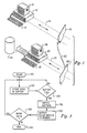
- Figure 1 is a pictorial representation of a system which may be utilized to implement the present invention;
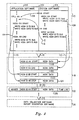
- Figure 2 is a schematic pictorial representation of the operation of an embodiment of the present invention;
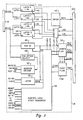
- Figure 3 is a generalized block diagram of a data output card which may be utilized with the present invention;
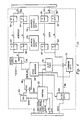
- Figure 4 is a generalized block diagram of a data collection card which may be utilized with the present invention; and
- Figure 5 is a logic flow chart illustrating the collection of monitoring data in accordance with an embodiment of the present invention.
- With reference now to the figures and in particular with reference to Figure 1, there is depicted a pictorial representation of a system which may be utilized to implement the present invention. As is illustrated, the system includes a
first processor 10 which is utilized to operate the software application under development. Typically, in the case of new software applications, the major portion of development of new applications is accomplished for a new generation of processors. For example,first processor 10 may comprise a new personal computer such as the PS/2 Personal Computer manufactured by International Business Machines Corporation of Armonk, New York, (PS/2 is a trade mark of International Business Machines Corporation) . Associated withfirst processor 10, in a manner known in the prior art, aredisplay 12 andkeyboard 14. Schematically indicated in association withfirst processor 10 isoutput bus 16. Those skilled in the art will appreciate thatoutput bus 16, in the case of a PS/2 Personal Computer will comprise a sixteen bit data bus. - A data output card 18 is coupled to
output bus 16 by means of an expansion slot or other connection means generally provided in the personal computer art. Data output card 18 is utilized to couple selected information regarding the monitoring of the software application under development withinfirst processor 10 todata collection card 22 viadedicated cable 20. -
Data collection card 22 is then utilized to associate a header or identifying frame of data with each frame of information concerning the monitoring of the software application under development, as well as a time tag to permit the chronological analysis of the software application under development. - Each frame of data which is utilized to monitor the software application under development within
first processor 10 is then coupled, via input/output bus 24 tosecond processor 26.Second processor 26 is preferably a personal computer and is typically a computer less advanced than the second generation machines for which new software applications are generally developed. For example, in the event a software application is being developed forfirst processor 10, whereinfirst processor 10 comprises a PS/2 Personal Computer,second processor 26 will typically be implemented utilizing a personal computer such as the PC-AT computer manufactured by International Business Machines Corporation.Second processor 26 will also generally include adisplay 28 and akeyboard 30 in a manner known in the prior art. Also associated withsecond processor 26 isdisk storage device 32 which may be utilized to store multiple frames of data relating to the development of the software application withinfirst processor 10. - Referring now to Figure 2, there is depicted a schematic pictorial representation of the operation of the present invention. Certain elements within Figure 2, although depicted schematically, are labelled with reference numerals which correspond to the pictorial representations of those elements within Figure 1, for the sake of clarity. As can be seen, Figure 2 includes a pictorial representation of
development software 100 which is resident withinfirst processor 10. In the depicted embodiment of the present invention,development software 100 includes bothapplication software 102 andsystem software 104. As is illustrated, upon the execution ofapplication software 102, the processing of the software will eventually encounter the step "CALL AA." Thereafter, as indicated by arrow 106, this reference to a portion of the system software will cause the program module AA to begin. At this point, in accordance with the method of the present invention, a uniquely identifiable element or "hook" is positioned within the software. This particular hook is referred to as "AA START." Thereafter, the method of the present invention will cause the identification of that hook to be written to the output bus, along with a frame of data which has been preselected to be output in conjunction with this particular hook. This data is then written viaoutput bus 16 into data output card 18, as illustrated at arrow 108. - The software application contained within the module AA then continues until the end of this module is encountered. Thereafter, in accordance with the illustrated embodiment of the present invention, a second hook "AA END" is encountered. This encountering of another hook will cause the hook identification and data associated therewith to be written to output
bus 16 and into data output card 18, as depicted atarrow 110. Thereafter, as indicated by arrow 112, software module AA ends and returns toapplication software 102. - The continued processing of
application software 102 will, in accordance with the depicted example, eventually encounter a third hook "BB START." Thereafter, as in the above example, the encountering of this hook will automatically cause an identification of the hook and an appropriate data frame to be written to outputbus 16 and into data output card 18, as illustrated atarrow 114. Finally, the hook "BB END," associated with the termination of this section ofapplication software 102, will be encountered and will similarly be written to outputbus 16 and into data output card 18, as indicated atarrow 116. - Still referring to Figure 2, the contents of data output card 18 are indicated in a schematic pictorial representation. As is illustrated, ID/data frames 118, 120, 122, and 124 are depicted within data output card 18. Those skilled in the art will appreciate that these ID/data frames are preferably coupled from
output bus 16 through data output card 18 todata collection card 22 viadedicated cable 20. Thus, it should be apparent that by utilizing the method of the present invention, it is possible to generate multiple frames of data, each frame including an identification of the hook element within the software application under development and a predetermined frame of data identifying specific details of the performance of the software application at that point. - Thereafter, each of these data frames is coupled to
data collection card 22, wherein a tagged data frame 126 is created for each data frame output from data output card 18. As is illustrated, tagged data frame 126 preferably includes a header or command byte which identifies the particular frame in question. Next, as discussed with regard to ID/data frames 118, 120, 122, and 124, tagged data frame 126 includes an identification of the particular hook in question and a frame of data associated therewith. Finally each tagged data frame 126 preferably includes a time tag which may be utilized to ascertain the chronological order in which the processes within the application program under development have been encountered. - Finally, input/
output bus 24 is utilized to couple a plurality of tagged data frames fromdata collection card 22 tosecond processor 26. At this point, those skilled in the art will appreciate that various data collection and report generation software packages may be utilized to assemble and publish reports which may be generated from the many tagged data frames which have been stored, thereby permitting the accurate monitoring of the software application under development. - Referring now to Figure 3, there is depicted a generalized block diagram of data output card 18 which may be utilized with the present invention. Those skilled in the art will appreciate that many different electronic configurations may be utilized with the present invention; however, Figure 3 is intended to be a general representation of the type of circuitry which may be utilized to implement the present invention.
- As may be seen, data output card 18 is coupled between
output bus 16 and todedicated cable 20. In the event thatfirst processor 10 comprises a PS/2 Personal Computer,output bus 16 will include sixteen data lines which may be written to by the processor withinfirst processor 10. As is illustrated, in the depicted embodiment of the present invention, data lines D0-D7 are coupled to latch 34 and 36 while data lines D8-D15 are coupled tolatches 38 and 40. By selective enablement of these latches it is possible to temporarily store data coupled fromoutput bus 16 and thereafter couple that data via data driver 42 to an output line which may be coupled, in a manner which will be explained in greater detail herein, todata collection card 22, viadedicated cable 20. - Also coupled to
output bus 16 are Programmable Option Select ID circuit 46 and Programmable Option Select circuit 48. These circuits are utilized, in a manner well known in the art in conjunction with the PS/2 Personal Computer to automatically provide the processor with an indication of the address and identification of each peripheral circuit card or device which is coupled tooutput bus 16. Address decode circuit 50 is preferably utilized to decode address bytes coupled to data output card 18. - Control logic/
state sequencer 54 is preferably implemented utilizing a programmable logic array and is utilized to generate control signals including: LAT 0,LAT 1,LAT 2, andLAT 3 which control the operation oflatches state sequencer 54 is utilized, in the depicted embodiment of Figure 3, to set a hook length flag, via length flag circuit 56. The hook length flag is utilized to provide an indication of whether or not the data being output fromfirst processor 10 consists of two bytes of data or four bytes of data. - Certain uniquely identifiable elements or "hooks" are inserted within the software application and are utilized to trace the performance of that software application during development. In the depicted embodiment of the present invention, these pieces of information may comprise either two bytes or four bytes of data and this information is coupled to
data collection card 22 via dedicatedcable 20 from length flag circuit 56. - In a manner which will be explained with regard to Figure 4, these signals are utilized by
data collection card 22 to generate control signals LS0 and LS1 which are coupled todemultiplexer 44 to sequentially enable the outputs oflatches first flag circuit 58 is utilized to generate a signal todata collection card 22 via dedicatedcable 20 to identify the first frame of data within each hook which is coupled todata collection card 22. This is preferably utilized to prevent confusion which may occur in the event of an interrupt or other discontinuity during the transmission of software application monitoring data. - Referring now to Figure 4, there is depicted a generalized block diagram of a
data collection card 22, which may be utilized with the present invention. As is illustrated, data fromdedicated cable 20, which has been coupled from data output card 18, is coupled via eight bit data latch 60 ontodata line 98. This data may be processed utilizing circuitry disclosed within this figure. -
Control circuit 62 is preferably implemented utilizing standard TTL logic circuits and may be varied to accommodate the approach desired to implement a software application monitoring and development technique in accordance with the present invention. As is illustrated,control circuit 62 is utilized to generate control signals LS0 and LSI, which operate demultiplexer 44 (see Figure 3) in response to half hook or full hook signals generated by control logic/state sequencer 54 of the data output card. -
Control circuit 62 also preferably enables the output ofoscillator 64 which operates at a frequency sufficient to permit the memory devices withindata collection card 22 to rapidly store data generated from data output card 18. In the depicted embodiment of the present invention an eight megahertz oscillator is utilized. The output ofoscillator 64 is then coupled toclock circuit 66, which acts to synchronize the pulses output fromoscillator 64 and provide a system clock signal. This clock signal is then coupled tostate sequencer 68 and address counter 78 to permit the accurate sequencing of the operations withindata collection card 22. - In conjunction with
state sequencer 68, sixteenbit timer 70 andcommand byte circuit 72 may be utilized to generate a time tag and command header data frame which are thereafter coupled todata line 98 to form a tagged data frame 126 (see Figure 2). - Next
data collection card 22 preferably utilizes a switched bank memory system to permit the rapid storing of data which has been output by data output card 18. This is particularly important in view of the fact that software applications for new generation processors are often developed and monitored by older generation machines and the speed differential in the processors involved make it imperative that the data collected during this monitoring process be stored as rapidly as possible. - In accordance with the embodiment depicted within
data collection card 22 of Figure 4, the system utilizes two separate memories,buffer 74 and buffer 76. As with known switched bank memory techniques, the data input viadata line 98 is preferably coupled via either Adata driver 90 or B data driver 94 to buffer 74 or buffer 76 respectively. Simultaneously, a thirteen bit address signal fromsecond processor 26 is coupled via input/output bus 24 intodata collection card 22 viaaddress line 80. This address information is then coupled to buffer 74 or buffer 76 byB address driver 88 or Aaddress driver 84 respectively. Address counter 78 is utilized, in a manner known in the art, to increment these addresses and couple the incremented address to buffer 74 or buffer 76 via Aaddress driver 82 orB address driver 86 respectively. - As those skilled in the art will appreciate,
data collection card 22 utilizesbuffer 74 and buffer 76 in a switched bank memory storage technique. That is, data is coupled, viadata line 98, intobuffer 74, via Adata driver 90 while B data driver 94 is not enabled. While data is being entered intobuffer 74, data previously entered into buffer 76 is being coupled out, via input/output bus 24, tosecond processor 26 by means of A data driver 92 whileB data driver 96 is inoperative. - Conversely, after
buffer 74 has been filled, data is coupled into buffer 76 via B data driver 94 while previously stored data is being coupled out ofbuffer 74 viaB data driver 96. In this manner, one buffer is always being filled while the other buffer is being emptied. This particular technique permits a current state-of-the-art processor to receive data at approximately twice normal speed, thus enabling the software monitoring and development system of the present invention to continuously record highly detailed trace information for long periods of time. In preferred embodiments, if one buffer becomes full before the other buffer is emptied, then a signal is generated and stored indicating data overflow. On subsequent runs some of the hooks may be removed to avoid such uncontrolled data loss. - Finally, with reference to Figure 5, there is depicted a logic flow chart illustrating the collection of monitoring data in accordance with the method of the present invention. As is illustrated, the process begins at
block 130 and thereafter proceeds to block 132 which illustrates the storing of data into a buffer within data collection card 22 (see Figure 4). Next, block 134 depicts a determination of whether or not the present buffer being utilized is full, and, if not, the process returns to block 132 and additional data is stored within that buffer. - In the event the buffer currently being utilized is full, as determined by
block 134, then block 136 illustrates the switching to a second buffer in the switched bank memory system ofdata collection card 22. Next, the data contained within the filled buffer is output to memory withinsecond processor 26, in the manner described above with respect to Figure 4. Thereafter, block 140 illustrates a determination of whether or not additional data is being received and if so, the process returns to block 132 which depicts the storing of additional data within a buffer. In the event no additional data has been received, then the process terminates, as illustrated in block 142. - Upon reference to the foregoing, it will be appreciated that the invention provides a software monitoring and development system which helps avoid the disadvantages of all known previous software monitoring and development techniques. By loading the software under development with a minimal number of uniquely identifiable elements or "hooks" and outputting a predetermined frame of data in association with each of these hooks, upon the encountering thereof, the processor overhead and output bus space required for known software based monitoring and development systems are not required.
- Next, by rapidly transferring these frames of data to a second processor, the problems associated with known hardware based software monitoring and development techniques are avoided. The analysis and tagging of each data frame associated with a particular hook may then be accomplished "off-line" by the second processor without the prospect of processor speed differences between a first generation processor and a second generation processor causing great gaps in the data accumulated from the software application under development.
- In this manner, the hybrid system disclosed herein permits the highly detailed trace of a software application during its development for long periods of time without unduly loading the processor being utilized or requiring a highly sophisticated high speed processor for hardware monitoring applications.
- In at least preferred embodiments the present invention provides an improved method and apparatus for software monitoring and development which permits the detailed tracing of software flow with continuous recording of high-volume performance trace data for an extended time span.
- While the invention has been particularly shown and described with reference to a preferred embodiment, it will be understood by those skilled in the art that various changes in form and detail may be made therein without departing from the scope of the invention.
Claims (13)
- A method for monitoring the performance of a selected software application within a first processor having an output bus, said method comprising the steps of:
inserting a limited number of uniquely identifiable elements at selected locations within said selected software application;
processing said software application within said first processor; and
automatically coupling to said output bus an identification of each of said uniquely identifiable elements, in association with a selected data frame, in response to the encountering of said uniquely identifiable elements during processing of said selected software application. - A method as claimed in Claim 1 further including the step of coupling a second processor having memory means associated therewith to said output bus and storing each of said identifications and said selected data frames within said memory means associated with said second processor.
- A method as claimed in Claim 2 further including the step of associating a time value with each of said identifications and said selected data frames prior to storage thereof.
- A method as claimed in any of Claims 2 or 3 further including the step of associating an identifying header frame with each of said identifications and said selected data frames prior to the storage thereof.
- A method as claimed in any of Claims 2 to 4 further including the step of storing within said memory means associated with said second processor an overrun indication in the event said identifications and said selected data frames are coupled to said output bus at a speed in excess of the speed at which said identifications and said selected data frames may be stored.
- An apparatus for monitoring the performance of a selected software application within a first processor having an output bus, comprising:
means for inserting a limited number of uniquely identifiable elements at selected locations within said selected software application;
means for automatically coupling to said output bus an identification of each of said uniquely identifiable elements in association with a selected data frame, in response to the encountering of said uniquely identifiable elements during processing of said selected software applications;
a second processor having memory means associated therewith; and
means for coupling said identifications and said selected data frames to said second processor for storage within said memory means associated therewith. - An apparatus as claimed in Claim 6 further including means for associating a time value with each of said identifications and selected data frames prior to storage thereof.
- An apparatus as claimed in Claim 7 further including means for generating an overrun indication in the event said identifications and said selected data frames are coupled to said memory means at a speed in excess of the speed at which said identifications and said selected data frames may be stored, and means for storing said overrun indication within said memory means associated with said second processor.
- An apparatus as claimed in any of Claims 6 to 8 wherein said memory means associated with said second processor includes a switched bank memory device.
- An apparatus as claimed in any of Claims 6 to 9 further including disk storage means coupled to said second processor.
- An apparatus as claimed in any of Claims 6 to 10 wherein said means for coupling said identifications and said selected data frames to said second processor includes a data output card coupled to said output bus of said first processor.
- An apparatus as claimed in Claim 11 wherein said means for coupling said identifications and said selected data frames to a second processor includes a data collection card coupled to said data output card by means of a dedicated cable.
- An apparatus as claimed in any of Claims 11 or 12 wherein said second processor includes an input bus and wherein said data collection card is coupled to said input bus.
Applications Claiming Priority (2)
| Application Number | Priority Date | Filing Date | Title |
|---|---|---|---|
| US458045 | 1989-12-27 | ||
| US07/458,045 US5121501A (en) | 1989-12-27 | 1989-12-27 | First processor inserting hooks into software and sending unique identifications to output bus and second processor associating data frames and time with these unique identifications |
Publications (3)
| Publication Number | Publication Date |
|---|---|
| EP0435499A2 true EP0435499A2 (en) | 1991-07-03 |
| EP0435499A3 EP0435499A3 (en) | 1992-06-17 |
| EP0435499B1 EP0435499B1 (en) | 1996-08-21 |
Family
ID=23819136
Family Applications (1)
| Application Number | Title | Priority Date | Filing Date |
|---|---|---|---|
| EP90313361A Expired - Lifetime EP0435499B1 (en) | 1989-12-27 | 1990-12-07 | Method and apparatus for software monitoring and development |
Country Status (4)
| Country | Link |
|---|---|
| US (1) | US5121501A (en) |
| EP (1) | EP0435499B1 (en) |
| JP (1) | JPH03202927A (en) |
| DE (1) | DE69028190T2 (en) |
Cited By (2)
| Publication number | Priority date | Publication date | Assignee | Title |
|---|---|---|---|---|
| EP0567722A2 (en) * | 1992-04-30 | 1993-11-03 | Hewlett-Packard Company | System for analyzing and debugging embedded software through dynamic and interactive use of code markers |
| US5754759A (en) * | 1993-09-29 | 1998-05-19 | U.S. Philips Corporation | Testing and monitoring of programmed devices |
Families Citing this family (26)
| Publication number | Priority date | Publication date | Assignee | Title |
|---|---|---|---|---|
| US5297274A (en) * | 1991-04-15 | 1994-03-22 | International Business Machines Corporation | Performance analysis of program in multithread OS by creating concurrently running thread generating breakpoint interrupts to active tracing monitor |
| US5333304A (en) * | 1991-05-03 | 1994-07-26 | International Business Machines Corporation | Method and apparatus for software application evaluation utilizing compiler applications |
| US5265254A (en) * | 1991-08-14 | 1993-11-23 | Hewlett-Packard Company | System of debugging software through use of code markers inserted into spaces in the source code during and after compilation |
| US5369770A (en) * | 1992-11-02 | 1994-11-29 | Microsoft Corporation | Standardized protected-mode interrupt manager |
| US5452457A (en) * | 1993-01-29 | 1995-09-19 | International Business Machines Corporation | Program construct and methods/systems for optimizing assembled code for execution |
| US5442740A (en) * | 1993-07-13 | 1995-08-15 | International Business Machines Corporation | Method and apparatus for visual display of program performance trace data |
| EP0679995B1 (en) * | 1994-04-26 | 2000-10-04 | Sun Microsystems, Inc. | Method and apparatus for encoding data to be self-describing |
| US5642478A (en) * | 1994-12-29 | 1997-06-24 | International Business Machines Corporation | Distributed trace data acquisition system |
| US5872909A (en) * | 1995-01-24 | 1999-02-16 | Wind River Systems, Inc. | Logic analyzer for software |
| WO1996038733A1 (en) * | 1995-06-02 | 1996-12-05 | Pure Software, Inc. | Remote monitoring of computer programs |
| US5778169A (en) * | 1995-08-07 | 1998-07-07 | Synopsys, Inc. | Computer system having improved regression testing |
| US5748878A (en) * | 1995-09-11 | 1998-05-05 | Applied Microsystems, Inc. | Method and apparatus for analyzing software executed in embedded systems |
| US5949972A (en) * | 1996-08-23 | 1999-09-07 | Compuware Corporation | System for memory error checking in an executable |
| US6106571A (en) * | 1998-01-29 | 2000-08-22 | Applied Microsystems Corporation | Relocatable instrumentation tags for testing and debugging a computer program |
| US6336184B1 (en) | 1998-08-14 | 2002-01-01 | International Business Machines Corporation | Method and apparatus for performing a trap operation in an information handling system |
| US6708180B1 (en) | 1998-08-14 | 2004-03-16 | International Business Machines Corporation | Method and apparatus for runtime remediation of object-code instructions in a computer program |
| US6973417B1 (en) | 1999-11-05 | 2005-12-06 | Metrowerks Corporation | Method and system for simulating execution of a target program in a simulated target system |
| US7093234B2 (en) * | 2001-08-24 | 2006-08-15 | International Business Machines Corporation | Dynamic CPU usage profiling and function call tracing |
| US6983453B2 (en) * | 2001-08-30 | 2006-01-03 | International Business Machines Corporation | Method and system for obtaining performance data from software compiled with or without trace hooks |
| US8015552B1 (en) | 2004-07-23 | 2011-09-06 | Green Hills Software, Inc. | Post-execution software debugger with coverage display |
| US8132159B1 (en) | 2004-07-23 | 2012-03-06 | Green Hills Software, Inc. | Post-execution software debugger with event display |
| US8136096B1 (en) | 2004-07-23 | 2012-03-13 | Green Hills Software, Inc. | Backward post-execution software debugger |
| US7653899B1 (en) | 2004-07-23 | 2010-01-26 | Green Hills Software, Inc. | Post-execution software debugger with performance display |
| US8271955B1 (en) | 2004-07-23 | 2012-09-18 | Green Hille Software, Inc. | Forward post-execution software debugger |
| CN103221926B (en) * | 2010-11-26 | 2015-09-30 | 三菱电机株式会社 | Program creating device and program creating method |
| WO2017023299A1 (en) * | 2015-08-04 | 2017-02-09 | Hewlett Packard Enterprise Development Lp | Composing future tests |
Family Cites Families (16)
| Publication number | Priority date | Publication date | Assignee | Title |
|---|---|---|---|---|
| US4445192A (en) * | 1980-11-25 | 1984-04-24 | Hewlett-Packard Company | Logic state analyzer with time and event count measurement between states |
| JPS57157362A (en) * | 1981-03-25 | 1982-09-28 | Hitachi Ltd | Method and apparatus of execution path career data pickup for architecture program |
| US4435759A (en) * | 1981-06-15 | 1984-03-06 | International Business Machines Corporation | Hardware monitor for obtaining processor software/hardware interrelationships |
| US4442491A (en) * | 1981-06-23 | 1984-04-10 | General Dynamics Corporation | Training evaluation process |
| JPS5816356A (en) * | 1981-07-20 | 1983-01-31 | Nec Corp | Measuring device for execution time of computer instruction |
| US4574351A (en) * | 1983-03-03 | 1986-03-04 | International Business Machines Corporation | Apparatus for compressing and buffering data |
| US4636940A (en) * | 1983-03-31 | 1987-01-13 | Hewlett-Packard Company | Logic analyzer using source program or other user defined symbols in the trace specification and the trace listing |
| US4660145A (en) * | 1984-02-03 | 1987-04-21 | Sundstrad Data Control, Inc. | System for compressing aircraft flight data utilizing a multilevel time format |
| US4651298A (en) * | 1984-05-30 | 1987-03-17 | The United States Of America As Represented By The Secretary Of The Air Force | Selection of data from busses for test |
| US4937740A (en) * | 1985-09-18 | 1990-06-26 | Cadre Technologies, Inc. | Real time software analyzing system for storing selective m-bit addresses based upon correspondingly generated n-bit tags |
| US4807282A (en) * | 1985-12-30 | 1989-02-21 | International Business Machines Corp. | Programmable P/C compatible communications card |
| US5051944A (en) * | 1986-04-17 | 1991-09-24 | Ncr Corporation | Computer address analyzer having a counter and memory locations each storing count value indicating occurrence of corresponding memory address |
| US4821178A (en) * | 1986-08-15 | 1989-04-11 | International Business Machines Corporation | Internal performance monitoring by event sampling |
| US4797881A (en) * | 1987-03-12 | 1989-01-10 | Sytek, Inc. | Bridge system for connecting networks |
| JPS63282539A (en) * | 1987-05-13 | 1988-11-18 | Nec Corp | Cpu time counting system for optional program section |
| US4827411A (en) * | 1987-06-15 | 1989-05-02 | International Business Machines Corporation | Method of maintaining a topology database |
-
1989
- 1989-12-27 US US07/458,045 patent/US5121501A/en not_active Expired - Lifetime
-
1990
- 1990-11-30 JP JP2330987A patent/JPH03202927A/en active Granted
- 1990-12-07 DE DE69028190T patent/DE69028190T2/en not_active Expired - Fee Related
- 1990-12-07 EP EP90313361A patent/EP0435499B1/en not_active Expired - Lifetime
Non-Patent Citations (3)
| Title |
|---|
| IBM TECHNICAL DISCLOSURE BULLETIN. vol. 30, no. 10, March 1988, NEW YORK US pages 251 - 253; 'Recording trace data in restrictive environments' * |
| IBM TECHNICAL DISCLOSURE BULLETIN. vol. 30, no. 6, November 1987, NEW YORK US pages 296 - 297; 'PERFORMANCE TRACE FACILITY' * |
| PROCEEDINGS OF THE IEEE 1988 NATIONAL AEROSPACE AND ELECTRONICS CONFERENCE NAECON 1988 vol. 2, 27 May 1988, DAYTON CONVENTION CENTER pages 620 - 623; MARC J. PITARYS: 'A built-in-support-function (BISF) for ADA software' * |
Cited By (3)
| Publication number | Priority date | Publication date | Assignee | Title |
|---|---|---|---|---|
| EP0567722A2 (en) * | 1992-04-30 | 1993-11-03 | Hewlett-Packard Company | System for analyzing and debugging embedded software through dynamic and interactive use of code markers |
| EP0567722A3 (en) * | 1992-04-30 | 1997-03-05 | Hewlett Packard Co | System for analyzing and debugging embedded software through dynamic and interactive use of code markers |
| US5754759A (en) * | 1993-09-29 | 1998-05-19 | U.S. Philips Corporation | Testing and monitoring of programmed devices |
Also Published As
| Publication number | Publication date |
|---|---|
| JPH0467219B2 (en) | 1992-10-27 |
| US5121501A (en) | 1992-06-09 |
| DE69028190D1 (en) | 1996-09-26 |
| EP0435499A3 (en) | 1992-06-17 |
| DE69028190T2 (en) | 1997-02-06 |
| EP0435499B1 (en) | 1996-08-21 |
| JPH03202927A (en) | 1991-09-04 |
Similar Documents
| Publication | Publication Date | Title |
|---|---|---|
| EP0435499B1 (en) | Method and apparatus for software monitoring and development | |
| US4769817A (en) | Concurrent fault simulation for logic designs | |
| US6789182B1 (en) | System and method for logging computer event data and physical components of a complex distributed system | |
| US4543626A (en) | Apparatus and method for controlling digital data processing system employing multiple processors | |
| EP0084431A2 (en) | Monitoring computer systems | |
| JP2776602B2 (en) | Test system and instruction execution sequence determination method | |
| EP0165517A2 (en) | Emulator for non-fixed instruction set VLSI devices | |
| EP0009678A1 (en) | Computer input/output apparatus | |
| US5715435A (en) | Trace control circuit in emulation system | |
| US6347335B1 (en) | System using a common and local event logs for logging event information generated by plurality of devices for determining problem in storage access operations | |
| US4752928A (en) | Transaction analyzer | |
| US4040037A (en) | Buffer chaining | |
| US7577878B2 (en) | Method for storing or transferring data using time sequencing | |
| EP0099462A2 (en) | Apparatus and method for buffering data in a data processing system | |
| US5964863A (en) | Method and apparatus for providing pipe fullness information external to a data processing system | |
| US4481582A (en) | Method and apparatus for enabling the tracing of errors occuring in a series of transfers of binary message words | |
| US5889948A (en) | Apparatus and method for inserting an address in a data stream through a FIFO buffer | |
| EP0543607B1 (en) | Image processing system | |
| EP0073081A1 (en) | Data processing system having a control device for controlling an intermediate memory during a bulk data transport between a source device and a destination device | |
| US3729716A (en) | Input/output channel | |
| US20030033552A1 (en) | Apparatus and method for wait state analysis in a digital signal processing system | |
| KR100259943B1 (en) | Apparatus and method for interfacing backplane to high speed micro-processor | |
| JP2500385B2 (en) | Input data management method | |
| US4748624A (en) | System for determining occurrence sequence of sampled data | |
| KR100298287B1 (en) | Apparatus and Method of Managing Messages in a System Bus |
Legal Events
| Date | Code | Title | Description |
|---|---|---|---|
| PUAI | Public reference made under article 153(3) epc to a published international application that has entered the european phase |
Free format text: ORIGINAL CODE: 0009012 |
|
| AK | Designated contracting states |
Kind code of ref document: A2 Designated state(s): DE FR GB IT |
|
| 17P | Request for examination filed |
Effective date: 19911018 |
|
| PUAL | Search report despatched |
Free format text: ORIGINAL CODE: 0009013 |
|
| AK | Designated contracting states |
Kind code of ref document: A3 Designated state(s): DE FR GB IT |
|
| 17Q | First examination report despatched |
Effective date: 19950222 |
|
| GRAH | Despatch of communication of intention to grant a patent |
Free format text: ORIGINAL CODE: EPIDOS IGRA |
|
| GRAH | Despatch of communication of intention to grant a patent |
Free format text: ORIGINAL CODE: EPIDOS IGRA |
|
| GRAA | (expected) grant |
Free format text: ORIGINAL CODE: 0009210 |
|
| AK | Designated contracting states |
Kind code of ref document: B1 Designated state(s): DE FR GB IT |
|
| PG25 | Lapsed in a contracting state [announced via postgrant information from national office to epo] |
Ref country code: IT Free format text: LAPSE BECAUSE OF FAILURE TO SUBMIT A TRANSLATION OF THE DESCRIPTION OR TO PAY THE FEE WITHIN THE PRESCRIBED TIME-LIMIT;WARNING: LAPSES OF ITALIAN PATENTS WITH EFFECTIVE DATE BEFORE 2007 MAY HAVE OCCURRED AT ANY TIME BEFORE 2007. THE CORRECT EFFECTIVE DATE MAY BE DIFFERENT FROM THE ONE RECORDED. Effective date: 19960821 Ref country code: FR Effective date: 19960821 |
|
| REF | Corresponds to: |
Ref document number: 69028190 Country of ref document: DE Date of ref document: 19960926 |
|
| EN | Fr: translation not filed | ||
| PLBE | No opposition filed within time limit |
Free format text: ORIGINAL CODE: 0009261 |
|
| STAA | Information on the status of an ep patent application or granted ep patent |
Free format text: STATUS: NO OPPOSITION FILED WITHIN TIME LIMIT |
|
| 26N | No opposition filed | ||
| PGFP | Annual fee paid to national office [announced via postgrant information from national office to epo] |
Ref country code: DE Payment date: 19981215 Year of fee payment: 9 |
|
| PG25 | Lapsed in a contracting state [announced via postgrant information from national office to epo] |
Ref country code: DE Free format text: LAPSE BECAUSE OF NON-PAYMENT OF DUE FEES Effective date: 20001003 |
|
| PGFP | Annual fee paid to national office [announced via postgrant information from national office to epo] |
Ref country code: GB Payment date: 20001204 Year of fee payment: 11 |
|
| PG25 | Lapsed in a contracting state [announced via postgrant information from national office to epo] |
Ref country code: GB Free format text: LAPSE BECAUSE OF NON-PAYMENT OF DUE FEES Effective date: 20011207 |
|
| REG | Reference to a national code |
Ref country code: GB Ref legal event code: IF02 |
|
| GBPC | Gb: european patent ceased through non-payment of renewal fee |
Effective date: 20011207 |