EP0409619A2 - A projection type image display apparatus - Google Patents
A projection type image display apparatus Download PDFInfo
- Publication number
- EP0409619A2 EP0409619A2 EP90307903A EP90307903A EP0409619A2 EP 0409619 A2 EP0409619 A2 EP 0409619A2 EP 90307903 A EP90307903 A EP 90307903A EP 90307903 A EP90307903 A EP 90307903A EP 0409619 A2 EP0409619 A2 EP 0409619A2
- Authority
- EP
- European Patent Office
- Prior art keywords
- light
- microlens array
- lens
- display device
- display apparatus
- Prior art date
- Legal status (The legal status is an assumption and is not a legal conclusion. Google has not performed a legal analysis and makes no representation as to the accuracy of the status listed.)
- Granted
Links
Images


Classifications
-
- G—PHYSICS
- G09—EDUCATION; CRYPTOGRAPHY; DISPLAY; ADVERTISING; SEALS
- G09F—DISPLAYING; ADVERTISING; SIGNS; LABELS OR NAME-PLATES; SEALS
- G09F13/00—Illuminated signs; Luminous advertising
-
- G—PHYSICS
- G03—PHOTOGRAPHY; CINEMATOGRAPHY; ANALOGOUS TECHNIQUES USING WAVES OTHER THAN OPTICAL WAVES; ELECTROGRAPHY; HOLOGRAPHY
- G03B—APPARATUS OR ARRANGEMENTS FOR TAKING PHOTOGRAPHS OR FOR PROJECTING OR VIEWING THEM; APPARATUS OR ARRANGEMENTS EMPLOYING ANALOGOUS TECHNIQUES USING WAVES OTHER THAN OPTICAL WAVES; ACCESSORIES THEREFOR
- G03B21/00—Projectors or projection-type viewers; Accessories therefor
- G03B21/14—Details
-
- G—PHYSICS
- G02—OPTICS
- G02B—OPTICAL ELEMENTS, SYSTEMS OR APPARATUS
- G02B3/00—Simple or compound lenses
- G02B3/0006—Arrays
- G02B3/0037—Arrays characterized by the distribution or form of lenses
- G02B3/005—Arrays characterized by the distribution or form of lenses arranged along a single direction only, e.g. lenticular sheets
-
- G—PHYSICS
- G02—OPTICS
- G02B—OPTICAL ELEMENTS, SYSTEMS OR APPARATUS
- G02B3/00—Simple or compound lenses
- G02B3/0006—Arrays
- G02B3/0037—Arrays characterized by the distribution or form of lenses
- G02B3/0056—Arrays characterized by the distribution or form of lenses arranged along two different directions in a plane, e.g. honeycomb arrangement of lenses
-
- G—PHYSICS
- G02—OPTICS
- G02F—OPTICAL DEVICES OR ARRANGEMENTS FOR THE CONTROL OF LIGHT BY MODIFICATION OF THE OPTICAL PROPERTIES OF THE MEDIA OF THE ELEMENTS INVOLVED THEREIN; NON-LINEAR OPTICS; FREQUENCY-CHANGING OF LIGHT; OPTICAL LOGIC ELEMENTS; OPTICAL ANALOGUE/DIGITAL CONVERTERS
- G02F1/00—Devices or arrangements for the control of the intensity, colour, phase, polarisation or direction of light arriving from an independent light source, e.g. switching, gating or modulating; Non-linear optics
- G02F1/01—Devices or arrangements for the control of the intensity, colour, phase, polarisation or direction of light arriving from an independent light source, e.g. switching, gating or modulating; Non-linear optics for the control of the intensity, phase, polarisation or colour
- G02F1/13—Devices or arrangements for the control of the intensity, colour, phase, polarisation or direction of light arriving from an independent light source, e.g. switching, gating or modulating; Non-linear optics for the control of the intensity, phase, polarisation or colour based on liquid crystals, e.g. single liquid crystal display cells
- G02F1/133—Constructional arrangements; Operation of liquid crystal cells; Circuit arrangements
- G02F1/1333—Constructional arrangements; Manufacturing methods
- G02F1/1335—Structural association of cells with optical devices, e.g. polarisers or reflectors
- G02F1/133526—Lenses, e.g. microlenses or Fresnel lenses
-
- G—PHYSICS
- G03—PHOTOGRAPHY; CINEMATOGRAPHY; ANALOGOUS TECHNIQUES USING WAVES OTHER THAN OPTICAL WAVES; ELECTROGRAPHY; HOLOGRAPHY
- G03B—APPARATUS OR ARRANGEMENTS FOR TAKING PHOTOGRAPHS OR FOR PROJECTING OR VIEWING THEM; APPARATUS OR ARRANGEMENTS EMPLOYING ANALOGOUS TECHNIQUES USING WAVES OTHER THAN OPTICAL WAVES; ACCESSORIES THEREFOR
- G03B21/00—Projectors or projection-type viewers; Accessories therefor
- G03B21/14—Details
- G03B21/20—Lamp housings
- G03B21/208—Homogenising, shaping of the illumination light
-
- H—ELECTRICITY
- H04—ELECTRIC COMMUNICATION TECHNIQUE
- H04N—PICTORIAL COMMUNICATION, e.g. TELEVISION
- H04N5/00—Details of television systems
- H04N5/74—Projection arrangements for image reproduction, e.g. using eidophor
- H04N5/7416—Projection arrangements for image reproduction, e.g. using eidophor involving the use of a spatial light modulator, e.g. a light valve, controlled by a video signal
- H04N5/7441—Projection arrangements for image reproduction, e.g. using eidophor involving the use of a spatial light modulator, e.g. a light valve, controlled by a video signal the modulator being an array of liquid crystal cells
Definitions
- the present invention relates generally to a display apparatus, and more particularly to a projection type display apparatus for displaying a projected color image through lenses from permissive display devices such as liquid crystal display devices wherein the color image is composed of multiple picture elements arranged in a matrix.
- This type of display apparatus is particularly applicable to a large-screen projection TV (television), information display systems and the like.
- the display devices used in the present invention do not emit light, but their transmissibility varies in response to a driving signal so as to display images and/or characters by modulating the intensity of an incident light.
- Examples of such display devices include liquid crystal displays, electrochromic displays, display units using transparent ceramics such as PLZT, among which the liquid crystal display devices are most widely used for pocket-sized TV and word processors.
- the commonly called “matrix type liquid crystal display device” contains picture elements arranged in a matrix that are individually driven by driving voltages so as to change the optical characteristics of the liquid crystal so as to make up images and/or characters.
- the driving voltage can be applied to the individual picture elements by various means, for example, by a simple matrix system or alternatively, by an active matrix system under which a non-linear two-terminal element such as MIM (metal-insulating layer-metal) or three-terminal switching element such as TFT (thin film transistor) is disposed for each picture element.
- MIM metal-insulating layer-metal
- TFT thin film transistor
- the transmissive type display devices can be observed; one is to observe the display panel directly, and the other is to observe a projected image enlarged through a lens.
- the projection type is classified into two categories; one is to use a single liquid crystal display panel equipped with a mosaic color filter of primary colors (i.e. red, green and blue) and the other is to use three liquid crystal display panels each representing a monochrome image.
- each display panel is illuminated with lights of primary colors, and makes up images of primary colors by representing a monochromatic image corresponding to color of the illumination.
- To compose the three images of primary colors one method is to project the images individually onto a screen and compose them thereon, and the other method is to compose them by use of a dichroic mirror and project the composed image through a common projecting lens.
- the active matrix liquid crystal display must employ signal lines among picture elements so as to drive anon-linear two-terminal element such as MIM (metal-insulating layer-metal) or three-terminal switching element such as TFT (thin film transistor) disposed for each picture element.
- MIM metal-insulating layer-metal
- TFT thin film transistor
- Part of incident rays to areas other than the picture elements is not subjected to modulation by display signals, and this part of the rays does not pass through the display element designed to display only in a "normally black mode" (a mode in which no ray is allowed to pass when no electric field is applied to the liquid crystal layer).
- a "normally black mode” a mode in which no ray is allowed to pass when no electric field is applied to the liquid crystal layer.
- the contrast of the image is reduced because of the increased black level.
- areas other than the picture elements are masked so as to absorb or reflect rays which do not contribute to the representation of images. In either case, the image is darkened because of the reduced aperture ratio throughout the display element. This defect is the some whether it is the directly observing type or the projection type.
- the projection type liquid crystal display apparatus use Kölhler's illumination.
- the optical system is constructed so that an image of the light source through a condenser lens is made up near projecting lens so as to minimize the diameter of the projection lens. If under this optical system a microlens array having a microlens for each picture element is used, the rays entered in the display devices are converged in each picture element area and modulated in response to a display signal, but after passing through the display areas, they diverge at angles depending upon numerical aperture (NA) of the microlens. When this angle is excessively large, a part of the rays passing through the display devices does not enter into the entrance pupil of the projecting lens, thereby resulting in dark images.
- NA numerical aperture
- Japanese Laid-Open Patent Publication (Kokai) No. 60-262131 discloses a pair of microlens arrays disposed at each side of the display device.
- the first microlens array converges a light entering the display device at a picture element area thereof
- the second microlens array converts the diverging rays at an angle determined by the numeral aperture of microlens array.
- This display apparatus requires a precise alignment of the display element and a pair of microlens arrays.
- the light passing through the display device is not exactly converted into a parallel flux owing to a possible aberration of the microlens array.
- the increased number of interfaces is likely to cause reflection loss and scattering of light.
- the projection type display apparatus of this invention which overcomes the above-discussed and numerous other disadvantages and deficiencies of the prior art, comprises a source of light, a transmissive display device having a number of picture elements, a light converging means for converging rays of light in correspondence to one or more of the picture elements, a projecting lens disposed backward of the display element so as to project the image represented by the display devices on a screen, the projection lens having a larger numerical aperture than that of the converging means.
- the converging means to comprises a microlens array.
- the converging means comprises a microlens array and a condenser lens.
- the microlens array is bonded to the display element with an adhesive selected from substances having a refractive index approximately within the difference of 0.1 to that of a material of which the microlens array is made.
- the invention described herein makes possible the objectives of providing a projection type display apparatus (1) which is capable of projecting an incident light to the display device effectively with the minimum loss, thereby enhancing the brightness of image, and (2) which is capable of easy and economical production.
- a liquid crystal display panel or device 1 (hereinafter referred to as "display device") having a pair of transparent substrate 1a such as glass sheets with a liquid crystal layer, picture element areas 1b and a light shield area 1c therebetween.
- the picture element area 1b is composed of pair of transmissive electrodes, and the light shield area 1c contains metallic conductors which transmit electrical signals to the transparent electrode.
- the area of the display device 1 has a diagonal of 75 mm, a picture element pitch of 190 ⁇ m (longitudinal) and 161 ⁇ m (lateral).
- the picture element area 1b has an area of 104 ⁇ m (longitudinal) x 88 ⁇ m (lateral), having an aperture ratio of 30%.
- Each substrate 1a has a refractive index n of 1.53, and a thickness of 1.1 mm.
- the liquid crystal display device is operated in the twisted nematic mode, but other modes of the liquid crystal display may be also utilized.
- a polarizer can be additionally used. In this case, the polarizer can be bonded to the display device 1 but in anticipation of a rise in temperature under a source of light having a high luminance, the direct attachment of the polarizer to the display device 1 is not recommendable.
- the polarizer can be located anywhere between the light source and the display device 1 provided that there is no substance which is likely to affect the polarizing characteristic of an incident light to the display device. For example, microlenses can be interposed the display device and the polarizer.
- the reference numeral 2 denotes a microlens array which functions as a convex lens.
- the microlens array 2 contains a number of microlenses 8 which each function as convex lenses.
- the microlens array includes compound eye lenses and lenticular lenses, which will be described below.
- the microlens array 2 is bonded to the display element 1 with a transparent adhesive in such a manner as to correspond to the picture elements 1b.
- a white source of light 3 is provided by a halogen lamp, a metal halide lamp, a xenon lamp and the like.
- a reflector 4 designed to reflect light in an opposite direction to the source of light, a condenser lens 5, a projecting lens 6 and a projection screen 7.
- the light from the source 3 is converged so as to advance toward the projecting lens 6 through the reflector 4 and the condenser lens 5.
- the light flux is converged through the microlens array 2 as shown in Figure 1, and passes through the picture element area 1b whereby the intensity is modulated in response to the application of a picture element signal voltage. Then the light is projected onto the screen 7 through the projecting lens 6.
- a pair of plano-convex lens having a focal length f of 180 mm are used with each convex face facing each other.
- the image of the light source will be formed at the right-hand focal point.
- the focal length of the condenser lens 5 is much larger than that of the microlenses, so that it is safely considered that the image of the light source through the microlenses is formed at the focal point of the microlenses.
- the rays passing through the picture element area 1b diverge in a conical shape within an angular range of tan ⁇ 1/9 around rays passing through the center of each microlens, and advance toward the projecting lens 6.
- L will be in the range between 155 and 180 mm.
- L is equal to 180 mm, the rays passing through the display element diverges within a circle having a radius of mm at the entrance pupil of the projection lens 6.
- NA numerical aperture
- the microlens array 2 contains microlenses 8 which are made by making such a material as to change the refractive index of a substrate 9 diffuse therein selectively through a suitable mask (not shown).
- Each of the microlenses 8 is semi-spherical, and has a higher refractive index area.
- alkaline ions or heavy metal ions can be used when the substrate 9 is glass, and organic molecules having a different molecular polarizability can be used when the substrate 9 is made of synthetic resin.
- FIG. 2 shows another example of converging means in the form of a fly eye lens 10 which is made of a transparent substance, and has a number of convex facets.
- this fly eye lens 10 each lens corresponds to picture element area.
- the microlens array 2 and the fly eye lens 10 are used in association with a display device shown in Figure 3.
- This display device has a transparent electrode 11 forming a picture element area.
- the electrode 11 is switched on by a thin film transistor (TFT) 15 in response to electric signals from metallic conductors 12 and 13, thereby activating the liquid crystal adjacent to the transparent electrode 11 (i.e. the picture element area 1b).
- TFT thin film transistor
- FIG 4 shows a further example in which each picture element 1b contains a plurality of electrode 11.
- the microlenses 8 and the lenses of the fly eye lens 10 can be disposed in each group of the electrodes 11.
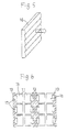
- Figure 5 shows a further example in which a lenticular lens 16 is used as a converging means.
- This lenticular lens 16 has convex facets on one side as shown in Figure 5, arranged at the same pitch as those of picture elements or twice the pitch of them, and converges light in one direction only.
- the lenticular lens 16 can be used in association with the display device shown in Figure 6.
- This display device is provided with electrodes 11 forming the picture element area lb between the metallic conductors 13.
- the electrodes 11 are switched on through non-linear element.
- the lenses of the lenticular lens 16 are arranged for each picture element area 1b.
- the present invention is applicable under Köhler's illumination, but it is also applicable under other illuminating systems such aS critical illumina tion and telecentric system.
- the present invention is applicable not only to a single display panel system but also to a three panel system.
- the adhesive unfavorably affects the optical characteristics thereof.
- the adhesive forms a layer thereby increasing the total thickness.
- the variations in thickness unfavorably affects the setting of the focal length of each component, and causes unnecessary reflection and diffusion.
- the liquid crystal panel or element 1 includes an inner layer 1a and an outer layer 1a′, containing liquid crystal 26 sealed by a sealing material 27.
- An adhesive is selected from substances having a refractive index (1.4 to 1.6) approximate to that of glass of which the microlens array is made and a viscosity of 100 to 2000cps.
- photosensitive adhesive made of acrylic or epoxy resin (e.g. AVR-100 manufactured by Threebond Inc., UV-1003 manufactured by Sonychemical Inc., and NOA-61, 63, 65 manufactured by Norland Inc.). These adhesives tend to harden by exposure to ultraviolet rays, but instead of them, a thermosetting resin can be used.
- the adhesive is coated on the liquid crystal element 1 to a thickness of 10 to 100 ⁇ m.
- a more intensified lamp must be used so as to shorten the curing time.
- a high pressure mercury lamp of 250W at a height of 6cm can be used without causing any problem, and the curing can be finished in 20 seconds.
- the reference numeral 23 denotes spacers which are contained in the adhesive layer so as to maintain the even surface.
- the spacers are plastic balls having a diameter of 10 to 100 ⁇ m, and a refractive index of 1.4 to 1.6, and such elasticity as to be below that of the adhesive. Preferably, several pieces are added per 1 mm3.
- the reference numeral 25 denotes extruded portions of the adhesive layer whereby the bond between the liquid crystal panel 1 and the microlens array 2 is maintained.
- Figure 8 shows that the liquid crystal panels and the microlens array 2 are curved when they are heated but the spacers 23 and the adhesive layer 24 are likewise curved, thereby preventing the inner layer 1a and the microlens array 2 from becoming separated.
- the microlens array 2 of soda-lime glass and the inner layer 1a were bonded with the adhesive layer 24 of 100 ⁇ m.
- the transmissibility was tested at 400 to 700nm.
- the loss caused by reflection was less than 0.1%, and no substantial scattering of light due to the presence of the spacers 23 was discerned.
- the inner layer 1a and the microlens array 2 were separated if the heating temperature is less than 100 o C.
- spacers 3 of 30 ⁇ m were used, no separation occurred at a temperature of 150 o C.
- the microlens array 2 can be made by the following methods:
Abstract
Description
- The present invention relates generally to a display apparatus, and more particularly to a projection type display apparatus for displaying a projected color image through lenses from permissive display devices such as liquid crystal display devices wherein the color image is composed of multiple picture elements arranged in a matrix. This type of display apparatus is particularly applicable to a large-screen projection TV (television), information display systems and the like.
- The display devices used in the present invention do not emit light, but their transmissibility varies in response to a driving signal so as to display images and/or characters by modulating the intensity of an incident light. Examples of such display devices include liquid crystal displays, electrochromic displays, display units using transparent ceramics such as PLZT, among which the liquid crystal display devices are most widely used for pocket-sized TV and word processors. By taking the liquid crystal display panels as an example, the background of the present invention will be described:
- The commonly called "matrix type liquid crystal display device" contains picture elements arranged in a matrix that are individually driven by driving voltages so as to change the optical characteristics of the liquid crystal so as to make up images and/or characters. The driving voltage can be applied to the individual picture elements by various means, for example, by a simple matrix system or alternatively, by an active matrix system under which a non-linear two-terminal element such as MIM (metal-insulating layer-metal) or three-terminal switching element such as TFT (thin film transistor) is disposed for each picture element. The present invention can be applied to either of these systems, but the greatest effect is achieved when it is applied to the active matrix system.
- There are at least two methods by which the transmissive type display devices can be observed; one is to observe the display panel directly, and the other is to observe a projected image enlarged through a lens. The projection type is classified into two categories; one is to use a single liquid crystal display panel equipped with a mosaic color filter of primary colors (i.e. red, green and blue) and the other is to use three liquid crystal display panels each representing a monochrome image. In the latter projection system each display panel is illuminated with lights of primary colors, and makes up images of primary colors by representing a monochromatic image corresponding to color of the illumination. To compose the three images of primary colors, one method is to project the images individually onto a screen and compose them thereon, and the other method is to compose them by use of a dichroic mirror and project the composed image through a common projecting lens.
- The above-mentioned single-panel system is disclosed in Japanese Laid-Open Patent Publication (Kokai) No. 49-74438 (allowed Publication No. 54-18886). This prior art discloses that thin film transistor controls picture panels individually, and an image is projected through color liquid crystal display devices equipped with filters of primary colors in mosaic and is observed. The employment of three liquid crystal display devices is discLosed in Japanese Laid-Open Patent Publication No. 60-179723.
- The active matrix liquid crystal display (LCD) must employ signal lines among picture elements so as to drive anon-linear two-terminal element such as MIM (metal-insulating layer-metal) or three-terminal switching element such as TFT (thin film transistor) disposed for each picture element. The provision of signal lines requires spaces, but the allowed space is limited in view of the electric performance and manufacturing convenience. If the picture element pitches are excessively minimized, the aperture ratio (the ratio of an effective opening occupied by each picture element or an area for allowing the passage of light to the total area) is reduced. Part of incident rays to areas other than the picture elements is not subjected to modulation by display signals, and this part of the rays does not pass through the display element designed to display only in a "normally black mode" (a mode in which no ray is allowed to pass when no electric field is applied to the liquid crystal layer). When the part of the rays is passed through a display panel designed to display only in a "normally white mode" (a mode in which the rays are allowed to pass when no electric field is applied to the liquid crystal panel), the contrast of the image is reduced because of the increased black level. To avoid poor contrast of image, areas other than the picture elements are masked so as to absorb or reflect rays which do not contribute to the representation of images. In either case, the image is darkened because of the reduced aperture ratio throughout the display element. This defect is the some whether it is the directly observing type or the projection type.
- As is the case with most conventional motion picture projectors and slide projectors, the projection type liquid crystal display apparatus use Kölhler's illumination. To use this illumination, the optical system is constructed so that an image of the light source through a condenser lens is made up near projecting lens so as to minimize the diameter of the projection lens. If under this optical system a microlens array having a microlens for each picture element is used, the rays entered in the display devices are converged in each picture element area and modulated in response to a display signal, but after passing through the display areas, they diverge at angles depending upon numerical aperture (NA) of the microlens. When this angle is excessively large, a part of the rays passing through the display devices does not enter into the entrance pupil of the projecting lens, thereby resulting in dark images.
- The numerical aperture (NA) is expressed by:
NA R/f
= 1/2F (1)
where R is the radius of the microlens and f is the focal length of the microlens, and F is the F number of microlens. - Japanese Laid-Open Patent Publication (Kokai) No. 60-262131 discloses a pair of microlens arrays disposed at each side of the display device. The first microlens array converges a light entering the display device at a picture element area thereof, and the second microlens array converts the diverging rays at an angle determined by the numeral aperture of microlens array. This display apparatus requires a precise alignment of the display element and a pair of microlens arrays. Furthermore, the light passing through the display device is not exactly converted into a parallel flux owing to a possible aberration of the microlens array. In addition, the increased number of interfaces is likely to cause reflection loss and scattering of light.
- The projection type display apparatus of this invention, which overcomes the above-discussed and numerous other disadvantages and deficiencies of the prior art, comprises a source of light, a transmissive display device having a number of picture elements, a light converging means for converging rays of light in correspondence to one or more of the picture elements, a projecting lens disposed backward of the display element so as to project the image represented by the display devices on a screen, the projection lens having a larger numerical aperture than that of the converging means.
- In another embodiment, the converging means to comprises a microlens array.
- In a further embodiment, the converging means comprises a microlens array and a condenser lens.
- According to another aspect of the present invention, the microlens array is bonded to the display element with an adhesive selected from substances having a refractive index approximately within the difference of 0.1 to that of a material of which the microlens array is made.
- Thus, the invention described herein makes possible the objectives of providing a projection type display apparatus (1) which is capable of projecting an incident light to the display device effectively with the minimum loss, thereby enhancing the brightness of image, and (2) which is capable of easy and economical production.
- This invention may be better understood and its numerous objects and advantages will become appar ent to those skilled in the art by reference to the accompanying drawings as follows:
- Figure 1 is a diagrammatic view showing an optical system incorporated in a projection type image display apparatus of a single panel system according to the present invention;
- Figure 2 is a perspective view showing a microlens array usable as a converging means for the present invention;
- Figures 3 and 4 are respectively plan views showing a liquid crystal display device used in association with the microlens array;
- Figure 5 is a perspective view showing a lenticular lens usable as a converging means for the present invention;
- Figure 6 is a schematic plan view showing a liquid crystal display device used in association with the lenticular lens of Figure 5;
- Figure 7 is a cross-sectional view showing a composite layer of a display device and a micro lens array; and
- Figure 8 is a cross-sectional view showing the composite layer of Figure 7 when it is heated.
- Referring to Figure 1, there is provided a liquid crystal display panel or device 1 (hereinafter referred to as "display device") having a pair of
transparent substrate 1a such as glass sheets with a liquid crystal layer,picture element areas 1b and alight shield area 1c therebetween. Thepicture element area 1b is composed of pair of transmissive electrodes, and thelight shield area 1c contains metallic conductors which transmit electrical signals to the transparent electrode. The area of thedisplay device 1 has a diagonal of 75 mm, a picture element pitch of 190µm (longitudinal) and 161 µm (lateral). Thepicture element area 1b has an area of 104µm (longitudinal) x 88 µm (lateral), having an aperture ratio of 30%. Eachsubstrate 1a has a refractive index n of 1.53, and a thickness of 1.1 mm. The liquid crystal display device is operated in the twisted nematic mode, but other modes of the liquid crystal display may be also utilized. A polarizer can be additionally used. In this case, the polarizer can be bonded to thedisplay device 1 but in anticipation of a rise in temperature under a source of light having a high luminance, the direct attachment of the polarizer to thedisplay device 1 is not recommendable. The polarizer can be located anywhere between the light source and thedisplay device 1 provided that there is no substance which is likely to affect the polarizing characteristic of an incident light to the display device. For example, microlenses can be interposed the display device and the polarizer. - The
reference numeral 2 denotes a microlens array which functions as a convex lens. Themicrolens array 2 contains a number of microlenses 8 which each function as convex lenses. The microlens array includes compound eye lenses and lenticular lenses, which will be described below. The pitches of the microlenses correspond to those of the picture elements in thedisplay element 1, and each microlens has a diameter of 160 µm, and a focal length equal to the thickness of thesubstrate 1a (in air, 1.1/1.53 = 0.72 mm). Accordingly, the numerical aperture NA of the microlens is 80/720 = 1/9. Themicrolens array 2 is bonded to thedisplay element 1 with a transparent adhesive in such a manner as to correspond to thepicture elements 1b. - For example, a white source of light 3 is provided by a halogen lamp, a metal halide lamp, a xenon lamp and the like.
- There is provided a reflector 4 designed to reflect light in an opposite direction to the source of light, a
condenser lens 5, a projecting lens 6 and aprojection screen 7. - The light from the source 3 is converged so as to advance toward the projecting lens 6 through the reflector 4 and the
condenser lens 5. The light flux is converged through themicrolens array 2 as shown in Figure 1, and passes through thepicture element area 1b whereby the intensity is modulated in response to the application of a picture element signal voltage. Then the light is projected onto thescreen 7 through the projecting lens 6. - In the embodiment shown in Figure 1 Kohler illumination is used, thereby enabling light passing through the center of the microlenses to advance toward the center of the projecting lens 6.
- For the condenser lens 5 a pair of plano-convex lens having a focal length f of 180 mm are used with each convex face facing each other. In Figure 1, if no
microlens array 2 is used, and the source of light 3 is placed toward the light incidence side of the left-hand lens as shown, the image of the light source will be formed at the right-hand focal point. - In Figure 1, if the
display element 1 is placed 10 mm to the right away from thecondenser lens 5, the distance between the source of light 3 and thedisplay element 1 will amount to 170 mm. In this situation, if themicrolens array 2 is placed at the place shown in Figure 1, which is substantially equal to the placement of a virtual source of light 170 mm backward (to the right) of themicrolens array 2. In this case, the image of the converged light source through themicrolens array 2 is formed at a place determined in the following manner: - In the formula of lens, 1/f = 1/a + 1/b a = -170 mm and f = 0.72 mm are placed in the formula
then
b = 1/(1/0.72 + 1/170) = 0.717 mm - As is evident from the calculation, the focal length of the
condenser lens 5 is much larger than that of the microlenses, so that it is safely considered that the image of the light source through the microlenses is formed at the focal point of the microlenses. The image of light source geometrically shrinks in size (focal length of themicrolens array 2/focal length of the condenser lens 5). In this example, the size will be reduced to 0.72/180 (=0.004 times). If the source of light 3 has a luminescent area of 10 mm in diameter, the reduced image of light source will be 40µm in diameter, which is smaller than thepicture element area 1b so as to allow all rays entered in the microlenses to pass therethrough. The rays passing through thepicture element area 1b diverge in a conical shape within an angular range of tan ϑ≦± 1/9 around rays passing through the center of each microlens, and advance toward the projecting lens 6. The distance L between thedisplay element 1 and the projection lens 6 is given by:
L = fp (1 + 1/m) (2)
where fp is the focal length of the projecting lens 6 and m is the magnification of projection. - If the focal length fp of the projecting lens 6 is 150 mm, and the magnification m is 5 to 30, L will be in the range between 155 and 180 mm. When L is equal to 180 mm, the rays passing through the display element diverges within a circle having a radius of mm at the entrance pupil of the projection lens 6. If the projection lens 6 has an entrance pupil having a diameter of 40 mm or more, all of the rays passing through the
display device 1 can be caught, Since the projection lens 6 has a numerical aperture (NA) of 20/150 = 1/7.5, which is larger by 20% than the numerical aperture (NA) of the microlens. It is essential to satisfy the conditions that the numerical aperture (NA) of themicrolens 2 is larger than that of the projection lens 6, preferably by 20%. Themicrolens array 2 contains microlenses 8 which are made by making such a material as to change the refractive index of a substrate 9 diffuse therein selectively through a suitable mask (not shown). Each of the microlenses 8 is semi-spherical, and has a higher refractive index area. As the substances alkaline ions or heavy metal ions can be used when the substrate 9 is glass, and organic molecules having a different molecular polarizability can be used when the substrate 9 is made of synthetic resin. - Figure 2 shows another example of converging means in the form of a
fly eye lens 10 which is made of a transparent substance, and has a number of convex facets. In thisfly eye lens 10 each lens corresponds to picture element area. - The
microlens array 2 and thefly eye lens 10 are used in association with a display device shown in Figure 3. This display device has atransparent electrode 11 forming a picture element area. Theelectrode 11 is switched on by a thin film transistor (TFT) 15 in response to electric signals frommetallic conductors picture element area 1b). - Figure 4 shows a further example in which each
picture element 1b contains a plurality ofelectrode 11. In this example the microlenses 8 and the lenses of the fly eye lens 10 (Figure 2) can be disposed in each group of theelectrodes 11. - Figure 5 shows a further example in which a
lenticular lens 16 is used as a converging means. Thislenticular lens 16 has convex facets on one side as shown in Figure 5, arranged at the same pitch as those of picture elements or twice the pitch of them, and converges light in one direction only. Thelenticular lens 16 can be used in association with the display device shown in Figure 6. This display device is provided withelectrodes 11 forming the picture element area lb between themetallic conductors 13. Theelectrodes 11 are switched on through non-linear element. The lenses of thelenticular lens 16 are arranged for eachpicture element area 1b. - Experiments have demonstrated that when the
microlens array 2 is used as shown in Figure 1, the brightness of the display image was doubled. - Experiments have also demonstrated that when the radius of the projecting lens 6 is less than 20 mm, the brightness varied depending upon the radius, but when it is greater than 20 mm, the brightness was constant regardless of variations in radius.
- The present invention is applicable under Köhler's illumination, but it is also applicable under other illuminating systems such aS critical illumina tion and telecentric system. The present invention is applicable not only to a single display panel system but also to a three panel system.
- There is a difficulty in bonding the
microlens array 2 to theliquid crystal element 1 because the adhesive unfavorably affects the optical characteristics thereof. In addition, the adhesive forms a layer thereby increasing the total thickness. The variations in thickness unfavorably affects the setting of the focal length of each component, and causes unnecessary reflection and diffusion. - Referring to Figures 7 and 8, the liquid crystal panel or
element 1 includes aninner layer 1a and anouter layer 1a′, containingliquid crystal 26 sealed by a sealingmaterial 27. An adhesive is selected from substances having a refractive index (1.4 to 1.6) approximate to that of glass of which the microlens array is made and a viscosity of 100 to 2000cps. For example, photosensitive adhesive made of acrylic or epoxy resin (e.g. AVR-100 manufactured by Threebond Inc., UV-1003 manufactured by Sonychemical Inc., and NOA-61, 63, 65 manufactured by Norland Inc.). These adhesives tend to harden by exposure to ultraviolet rays, but instead of them, a thermosetting resin can be used. The adhesive is coated on theliquid crystal element 1 to a thickness of 10 to 100 µm. When the adhesive coat is thick, a more intensified lamp must be used so as to shorten the curing time. For example, when the coat is 100 µm thick, a high pressure mercury lamp of 250W at a height of 6cm can be used without causing any problem, and the curing can be finished in 20 seconds. - The
reference numeral 23 denotes spacers which are contained in the adhesive layer so as to maintain the even surface. The spacers are plastic balls having a diameter of 10 to 100µm, and a refractive index of 1.4 to 1.6, and such elasticity as to be below that of the adhesive. Preferably, several pieces are added per 1 mm³. Thereference numeral 25 denotes extruded portions of the adhesive layer whereby the bond between theliquid crystal panel 1 and themicrolens array 2 is maintained. - Figure 8 shows that the liquid crystal panels and the
microlens array 2 are curved when they are heated but thespacers 23 and theadhesive layer 24 are likewise curved, thereby preventing theinner layer 1a and themicrolens array 2 from becoming separated. - Experiments have demonstrated that the
microlens array 2 of soda-lime glass and theinner layer 1a were bonded with theadhesive layer 24 of 100 µm. The transmissibility was tested at 400 to 700nm. The loss caused by reflection was less than 0.1%, and no substantial scattering of light due to the presence of thespacers 23 was discerned. When no spacer was used, theinner layer 1a and themicrolens array 2 were separated if the heating temperature is less than 100oC. In contrast, when spacers 3 of 30 µm were used, no separation occurred at a temperature of 150oC. In addition, theinner layer 1a and the microlens array unit withheld thermal shock tests between -25oC and 80oC (100 cycles). - The
microlens array 2 can be made by the following methods: - (1) A molding method in which a metal mold is used to form a synthetic resin material or glass into a microlens array.
- (2) A method in which convex lenses in a microlens array are formed by utilizing a phenomenon that when a specific type of photosensitive resin is exposed to light in a pattern corresponding to the microlens array, the non-reacted photosensitive resin moves from the non-exposed area to the exposed area and the exposed area swells up to form the convex lenses.
- (3) A method in which convex lenses in a microlens array are formed by using a known photolithographic technique to pattern a thermoplastic resin in a plate shape corresponding to the microlens array and then heating the resin to a temperature above its softening point to give it flowability and cause semispherical surface by surface tension.
- (4) A method in which convex lenses in a microlens array are formed by performing the proximity exposure on a photosensitive resin and distributing the amount of photoreacted material according to the indistinctness of the transfer image on the photosensitive resin at the edges of the mask used in the proximity exposure.
- (5) A method in which a configuration equivalent to a microlens array is obtained by irradiating light with an intensity distribution on a photosensitive resin to form a refractive index distribution corresponding to the intensity of the light.
- (6) A method in which a configuration equivalent to a microlens array is obtained by forming a refractive index distribution on glass or other transparent substrate using a selective ion exchange technique.
- (7) A method in which convex lenses in a microlens array are formed by utilizing the contraction which accompanies crystallization when light is applied to a photosensitive glass.
- It is understood that various other modifications will be apparent to and can be readily made by those skilled in the art without departing from the scope and spirit of this invention. Accordingly, it is not intended that the scope of the claims appended hereto be limited to the description as set forth herein, but rather that the claims be construed as encompassing all the features of patentable novelty that reside in the present invention, including all features that would be treated as equivalents thereof by those skilled in the art to which this invention pertains.
Claims (4)
Applications Claiming Priority (2)
| Application Number | Priority Date | Filing Date | Title |
|---|---|---|---|
| JP1187714A JP2815910B2 (en) | 1989-07-19 | 1989-07-19 | Projection image display device |
| JP187714/89 | 1989-07-19 |
Publications (3)
| Publication Number | Publication Date |
|---|---|
| EP0409619A2 true EP0409619A2 (en) | 1991-01-23 |
| EP0409619A3 EP0409619A3 (en) | 1991-09-25 |
| EP0409619B1 EP0409619B1 (en) | 1995-09-20 |
Family
ID=16210890
Family Applications (1)
| Application Number | Title | Priority Date | Filing Date |
|---|---|---|---|
| EP90307903A Expired - Lifetime EP0409619B1 (en) | 1989-07-19 | 1990-07-19 | A projection type image display apparatus |
Country Status (5)
| Country | Link |
|---|---|
| US (1) | US5056912A (en) |
| EP (1) | EP0409619B1 (en) |
| JP (1) | JP2815910B2 (en) |
| KR (1) | KR940000589B1 (en) |
| DE (1) | DE69022505T2 (en) |
Cited By (9)
| Publication number | Priority date | Publication date | Assignee | Title |
|---|---|---|---|---|
| EP0534426A2 (en) * | 1991-09-26 | 1993-03-31 | Canon Kabushiki Kaisha | Liquid crystal display panel and projector utilizing the same |
| US5548349A (en) * | 1993-12-27 | 1996-08-20 | Sharp Kabushiki Kaisha | Transmission type color liquid display apparatus with first and second lens layers located between a white light source and the display device |
| EP0930523A1 (en) * | 1998-01-19 | 1999-07-21 | Matsushita Electronics Corporation | Liquid crystal display device |
| EP0952473A1 (en) * | 1997-10-09 | 1999-10-27 | Seiko Epson Corporation | Projection type display |
| US6137555A (en) * | 1997-03-26 | 2000-10-24 | Matsushita Electronics Corporation | Liquid crystal panel with uniform adhesive layer and method of manufacturing |
| AU764904B2 (en) * | 1997-10-09 | 2003-09-04 | Seiko Epson Corporation | Projection display device |
| EP1521479A1 (en) * | 2003-10-02 | 2005-04-06 | Thomson Licensing S.A. | Projector device with lens array |
| US7489291B2 (en) | 1996-09-27 | 2009-02-10 | Semiconductor Energy Laboratory Co., Ltd. | Electrooptical device and method of fabricating the same |
| US9147368B2 (en) | 2007-12-03 | 2015-09-29 | Semiconductor Energy Laboratory Co., Ltd. | TFT arrangement for display device |
Families Citing this family (48)
| Publication number | Priority date | Publication date | Assignee | Title |
|---|---|---|---|---|
| ES2077648T3 (en) * | 1989-07-19 | 1995-12-01 | Sharp Kk | IMAGE PRESENTATION DEVICE. |
| US5187599A (en) * | 1990-02-01 | 1993-02-16 | Sharp Kabushiki Kaisha | Display including two microlens arrays with unequal focal lengths and congruent focal points |
| US5317436A (en) * | 1990-12-31 | 1994-05-31 | Kopin Corporation | A slide assembly for projector with active matrix moveably mounted to housing |
| US5666175A (en) * | 1990-12-31 | 1997-09-09 | Kopin Corporation | Optical systems for displays |
| US5396304A (en) * | 1990-12-31 | 1995-03-07 | Kopin Corporation | Slide projector mountable light valve display |
| JP2831510B2 (en) * | 1991-03-14 | 1998-12-02 | 株式会社日立製作所 | Liquid crystal display element and liquid crystal display device using the same |
| KR960011399B1 (en) * | 1991-04-03 | 1996-08-22 | 샤프 가부시끼가이샤 | Apparatus for assembling an optical device |
| US5299289A (en) * | 1991-06-11 | 1994-03-29 | Matsushita Electric Industrial Co., Ltd. | Polymer dispersed liquid crystal panel with diffraction grating |
| JPH0527114A (en) * | 1991-07-25 | 1993-02-05 | Sharp Corp | Production of organic color filter array and projection type color liquid crystal display device |
| JPH05341269A (en) * | 1992-06-05 | 1993-12-24 | Matsushita Electric Ind Co Ltd | Light valve device and display device using the device |
| JPH06102509A (en) * | 1992-06-17 | 1994-04-15 | Xerox Corp | Full-color display device having optical coupling lens array |
| JP2528420B2 (en) * | 1992-07-02 | 1996-08-28 | 信号電材株式会社 | External light reflection prevention device for signal lights |
| US5689315A (en) * | 1992-07-15 | 1997-11-18 | Matsushita Electric Industrial Co., Ltd. | Light valve apparatus which is employed in a projection display system and in a view-finder system |
| JP3207022B2 (en) * | 1992-11-24 | 2001-09-10 | 株式会社日立製作所 | Light source, illumination device, and liquid crystal projection display device for projection display device |
| US5583396A (en) * | 1993-03-18 | 1996-12-10 | Matsushita Electric Industrial Co., Ltd. | Optical device with metal halide discharge lamp having enhanced starting property |
| US5617152A (en) * | 1993-06-20 | 1997-04-01 | Unic View Ltd. | Projector system for video and computer generated information |
| US5706062A (en) * | 1993-06-20 | 1998-01-06 | Unic View Ltd. | Projector system including keystone correction |
| US5398125A (en) * | 1993-11-10 | 1995-03-14 | Minnesota Mining And Manufacturing Company | Liquid crystal projection panel having microlens arrays, on each side of the liquid crystal, with a focus beyond the liquid crystal |
| KR0131570B1 (en) * | 1993-11-30 | 1998-04-16 | 배순훈 | Optical path regulating apparatus for projector |
| JPH07225303A (en) * | 1993-12-16 | 1995-08-22 | Sharp Corp | Microlens substrate, liquid crystal display element using the same, and liquid crystal projector device |
| US5664859A (en) * | 1994-01-03 | 1997-09-09 | Kopin Corporation | Projection display docking system |
| KR100220673B1 (en) * | 1994-01-18 | 1999-09-15 | 전주범 | Projection type image display apparatus |
| US5550604A (en) * | 1994-06-03 | 1996-08-27 | Kopin Corporation | Compact high resolution light valve projector |
| US5806950A (en) * | 1994-06-03 | 1998-09-15 | Kopin Corporation | Compact high resolution light valve projector |
| US6545653B1 (en) * | 1994-07-14 | 2003-04-08 | Matsushita Electric Industrial Co., Ltd. | Method and device for displaying image signals and viewfinder |
| US5630659A (en) * | 1994-09-28 | 1997-05-20 | Kopin Corporation | Compact high resolution light valve projector |
| US5719706A (en) * | 1995-03-15 | 1998-02-17 | Matsushita Electric Industrial Co., Ltd. | Illuminating apparatus, projection lens, and display apparatus including the illumination apparatus and the projection lens |
| US5576599A (en) * | 1995-06-07 | 1996-11-19 | Hughes Aircraft Company | Low EMI high intensity discharge RF driven lamp |
| JPH0990337A (en) * | 1995-09-28 | 1997-04-04 | Sharp Corp | Transmission type liquid crystal display device |
| US5973844A (en) * | 1996-01-26 | 1999-10-26 | Proxemics | Lenslet array systems and methods |
| US6124974A (en) * | 1996-01-26 | 2000-09-26 | Proxemics | Lenslet array systems and methods |
| JPH09230321A (en) * | 1996-02-20 | 1997-09-05 | Denso Corp | Color liquid crystal display device |
| US5836096A (en) * | 1996-03-04 | 1998-11-17 | Brauer; William R. | Apparatus for illuminating medical diagnostic imaging film with enhanced viewability |
| JP3195238B2 (en) * | 1996-06-18 | 2001-08-06 | シャープ株式会社 | Projection type color liquid crystal display |
| US5880887A (en) * | 1996-08-16 | 1999-03-09 | Dai Nippon Printing Co., Ltd. | Lenticular lens sheet, display front plate and transmission type projection screen |
| US5940998A (en) * | 1996-09-06 | 1999-08-24 | Brauer; William R. | Illuminating apparatus for use with medical diagnostic imaging film |
| JPH10254370A (en) * | 1997-03-10 | 1998-09-25 | Canon Inc | Display panel and projection type display device using it |
| US5990992A (en) * | 1997-03-18 | 1999-11-23 | Nippon Sheet Glass Co., Ltd. | Image display device with plural planar microlens arrays |
| US6798390B1 (en) * | 1997-08-29 | 2004-09-28 | Canon Kabushiki Kaisha | 3D image reconstructing apparatus and 3D object inputting apparatus |
| JPH11231314A (en) * | 1998-02-16 | 1999-08-27 | Micro Opt:Kk | Liquid crystal display element |
| JP2001188107A (en) * | 1999-12-28 | 2001-07-10 | Seiko Epson Corp | Method for producing microlens substrate, microlens substrate, counter substrate for liquid crystal panel, liquid crystal panel and projective display device |
| JP2002122707A (en) * | 2000-10-13 | 2002-04-26 | Canon Inc | Aspheric microstructure and method for manufacturing the same |
| JP2004118153A (en) * | 2002-09-30 | 2004-04-15 | Mitsubishi Electric Corp | Projection display device |
| JP4379056B2 (en) * | 2003-08-12 | 2009-12-09 | 富士ゼロックス株式会社 | Three-dimensional imaging apparatus and method |
| KR101263697B1 (en) * | 2006-06-27 | 2013-05-10 | 엘지디스플레이 주식회사 | lenticular array and image display device including the same |
| US8724040B2 (en) * | 2011-11-02 | 2014-05-13 | Chimei Innolux Corporation | Pixel structures of 3D display devices |
| CN104021732B (en) * | 2014-05-22 | 2017-01-18 | 京东方科技集团股份有限公司 | Display device |
| US11307351B2 (en) * | 2018-12-07 | 2022-04-19 | Electronics And Telecommunications Research Institute | Apparatus and method for shaping optical waveform |
Citations (2)
| Publication number | Priority date | Publication date | Assignee | Title |
|---|---|---|---|---|
| JPS6014220A (en) * | 1983-07-06 | 1985-01-24 | Canon Inc | Color display device and its displaying method |
| JPS6435416A (en) * | 1987-07-30 | 1989-02-06 | Matsushita Electric Ind Co Ltd | Liquid crystal panel |
Family Cites Families (14)
| Publication number | Priority date | Publication date | Assignee | Title |
|---|---|---|---|---|
| US3840695A (en) * | 1972-10-10 | 1974-10-08 | Westinghouse Electric Corp | Liquid crystal image display panel with integrated addressing circuitry |
| US3877801A (en) * | 1973-12-20 | 1975-04-15 | Itek Corp | Image translation apparatus |
| US4082438A (en) * | 1975-05-30 | 1978-04-04 | Rca Corporation | Zero-order diffractive subtractive filter projector |
| JPS5418886A (en) * | 1977-07-12 | 1979-02-13 | Mitsubishi Chem Ind Ltd | Production of olefin polymer |
| JPS58147708A (en) * | 1982-02-26 | 1983-09-02 | Nippon Kogaku Kk <Nikon> | Optical device for illumination |
| US4428647A (en) * | 1982-11-04 | 1984-01-31 | Xerox Corporation | Multi-beam optical system using lens array |
| JPS60177788A (en) * | 1984-02-23 | 1985-09-11 | Seiko Epson Corp | Twin-lens stereo picture display device |
| JPS60179723A (en) * | 1984-02-27 | 1985-09-13 | Sharp Corp | Liquid crystal projection device |
| JPS60262131A (en) * | 1984-06-08 | 1985-12-25 | Sharp Corp | Liquid-crystal display device |
| JPH0623817B2 (en) * | 1985-07-18 | 1994-03-30 | 旭光学工業株式会社 | LCD projection image display device |
| GB8804402D0 (en) * | 1988-02-25 | 1988-03-23 | Emi Plc Thorn | Display device |
| JPH0255384A (en) * | 1988-08-22 | 1990-02-23 | Seiko Epson Corp | Projection type display device |
| US4952026A (en) * | 1988-10-14 | 1990-08-28 | Corning Incorporated | Integral optical element and method |
| JPH02262185A (en) * | 1989-03-31 | 1990-10-24 | Sharp Corp | Projection type display device |
-
1989
- 1989-07-19 JP JP1187714A patent/JP2815910B2/en not_active Expired - Lifetime
-
1990
- 1990-07-17 US US07/553,084 patent/US5056912A/en not_active Expired - Lifetime
- 1990-07-19 DE DE69022505T patent/DE69022505T2/en not_active Expired - Lifetime
- 1990-07-19 KR KR1019900010988A patent/KR940000589B1/en not_active IP Right Cessation
- 1990-07-19 EP EP90307903A patent/EP0409619B1/en not_active Expired - Lifetime
Patent Citations (2)
| Publication number | Priority date | Publication date | Assignee | Title |
|---|---|---|---|---|
| JPS6014220A (en) * | 1983-07-06 | 1985-01-24 | Canon Inc | Color display device and its displaying method |
| JPS6435416A (en) * | 1987-07-30 | 1989-02-06 | Matsushita Electric Ind Co Ltd | Liquid crystal panel |
Non-Patent Citations (2)
| Title |
|---|
| PATENT ABSTRACTS OF JAPAN, vol. 13, no. 222 (P-876)[3570], 24th May 1989; & JP-A-1 35 416 (MATSUSHITA) 06-02-1989 * |
| PATENT ABSTRACTS OF JAPAN, vol. 9, no. 129 (P-361)[1852], 5th June 1985; & JP-A-60 14 220 (CANON) 24-01-1985 * |
Cited By (17)
| Publication number | Priority date | Publication date | Assignee | Title |
|---|---|---|---|---|
| EP0534426A2 (en) * | 1991-09-26 | 1993-03-31 | Canon Kabushiki Kaisha | Liquid crystal display panel and projector utilizing the same |
| EP0534426A3 (en) * | 1991-09-26 | 1993-06-16 | Canon Kabushiki Kaisha | Liquid crystal display panel and projector utilizing the same |
| US5764318A (en) * | 1991-09-26 | 1998-06-09 | Canon Kabushiki Kaisha | Liquid crystal display panel and projector utilizing the same |
| US5548349A (en) * | 1993-12-27 | 1996-08-20 | Sharp Kabushiki Kaisha | Transmission type color liquid display apparatus with first and second lens layers located between a white light source and the display device |
| US8564575B2 (en) | 1996-09-27 | 2013-10-22 | Semiconductor Energy Laboratory Co., Ltd. | Electrooptical device and method of fabricating the same |
| US7532208B2 (en) | 1996-09-27 | 2009-05-12 | Semiconductor Energy Laboratory Co., Ltd. | Electrooptical device and method of fabricating the same |
| US7489291B2 (en) | 1996-09-27 | 2009-02-10 | Semiconductor Energy Laboratory Co., Ltd. | Electrooptical device and method of fabricating the same |
| US6137555A (en) * | 1997-03-26 | 2000-10-24 | Matsushita Electronics Corporation | Liquid crystal panel with uniform adhesive layer and method of manufacturing |
| AU764904B2 (en) * | 1997-10-09 | 2003-09-04 | Seiko Epson Corporation | Projection display device |
| AU764831B2 (en) * | 1997-10-09 | 2003-09-04 | Seiko Epson Corporation | Projection display device |
| KR100489459B1 (en) * | 1997-10-09 | 2005-05-16 | 세이코 엡슨 가부시키가이샤 | Projection type display |
| EP0952473A4 (en) * | 1997-10-09 | 2001-08-29 | Seiko Epson Corp | Projection type display |
| EP0952473A1 (en) * | 1997-10-09 | 1999-10-27 | Seiko Epson Corporation | Projection type display |
| EP0930523A1 (en) * | 1998-01-19 | 1999-07-21 | Matsushita Electronics Corporation | Liquid crystal display device |
| EP1521479A1 (en) * | 2003-10-02 | 2005-04-06 | Thomson Licensing S.A. | Projector device with lens array |
| US9147368B2 (en) | 2007-12-03 | 2015-09-29 | Semiconductor Energy Laboratory Co., Ltd. | TFT arrangement for display device |
| US9423657B2 (en) | 2007-12-03 | 2016-08-23 | Semiconductor Energy Laboratory Co., Ltd. | TFT arrangement for display device |
Also Published As
| Publication number | Publication date |
|---|---|
| DE69022505T2 (en) | 1996-04-18 |
| EP0409619B1 (en) | 1995-09-20 |
| KR910003553A (en) | 1991-02-27 |
| DE69022505D1 (en) | 1995-10-26 |
| US5056912A (en) | 1991-10-15 |
| KR940000589B1 (en) | 1994-01-26 |
| JPH0351882A (en) | 1991-03-06 |
| JP2815910B2 (en) | 1998-10-27 |
| EP0409619A3 (en) | 1991-09-25 |
Similar Documents
| Publication | Publication Date | Title |
|---|---|---|
| EP0409619B1 (en) | A projection type image display apparatus | |
| KR940000590B1 (en) | Image display device | |
| EP0465171B1 (en) | A colour liquid crystal display device | |
| US5337186A (en) | Transmissive image display device | |
| JP2002182008A (en) | Optical lens system, image display device, microlens array, liquid crystal display element and projection type liquid crystal display device | |
| JP2002107519A (en) | Reflection type display unit, retroreflector | |
| US5359440A (en) | Image display apparatus with microlens plate having mutually fused together lenses resulting in hexagonal shaped microlenses | |
| JP2849492B2 (en) | Projection type liquid crystal display | |
| EP0425251A2 (en) | Image display apparatus | |
| JP2000193928A (en) | Optical modulating element and image projection display device | |
| JP2008097032A (en) | Micro-lens array, liquid crystal display element, and liquid crystal display device of projection-type | |
| JPH0430140A (en) | Projection type color liquid crystal display device | |
| JPH05346566A (en) | Projection type color image display device | |
| JPH049922A (en) | Projection type color liquid crystal display device | |
| EP0409620B1 (en) | A projection type color image display device | |
| JPH083583B2 (en) | Projection color display device | |
| JPH1184337A (en) | Liquid crystal device and projection display device | |
| JP3452020B2 (en) | projector | |
| JPH06242411A (en) | Light valve device and display device using it | |
| JPH06222355A (en) | Light valve device and display device using it | |
| JP2000131507A (en) | Lens array plate, light valve device, projection type display device, and viewfinder device | |
| EP0438910A2 (en) | A projection type display apparatus | |
| JPH0363626A (en) | Projection type color liquid crystal display device | |
| JPH09304762A (en) | Color liquid crystal display device and its production | |
| JPH0462532A (en) | Projection type image display device |
Legal Events
| Date | Code | Title | Description |
|---|---|---|---|
| PUAI | Public reference made under article 153(3) epc to a published international application that has entered the european phase |
Free format text: ORIGINAL CODE: 0009012 |
|
| AK | Designated contracting states |
Kind code of ref document: A2 Designated state(s): DE FR GB NL |
|
| 17P | Request for examination filed |
Effective date: 19901228 |
|
| PUAL | Search report despatched |
Free format text: ORIGINAL CODE: 0009013 |
|
| AK | Designated contracting states |
Kind code of ref document: A3 Designated state(s): DE FR GB NL |
|
| 17Q | First examination report despatched |
Effective date: 19940119 |
|
| GRAA | (expected) grant |
Free format text: ORIGINAL CODE: 0009210 |
|
| AK | Designated contracting states |
Kind code of ref document: B1 Designated state(s): DE FR GB NL |
|
| REF | Corresponds to: |
Ref document number: 69022505 Country of ref document: DE Date of ref document: 19951026 |
|
| ET | Fr: translation filed | ||
| PLBE | No opposition filed within time limit |
Free format text: ORIGINAL CODE: 0009261 |
|
| STAA | Information on the status of an ep patent application or granted ep patent |
Free format text: STATUS: NO OPPOSITION FILED WITHIN TIME LIMIT |
|
| 26N | No opposition filed | ||
| REG | Reference to a national code |
Ref country code: GB Ref legal event code: IF02 |
|
| PGFP | Annual fee paid to national office [announced via postgrant information from national office to epo] |
Ref country code: FR Payment date: 20090710 Year of fee payment: 20 |
|
| PGFP | Annual fee paid to national office [announced via postgrant information from national office to epo] |
Ref country code: NL Payment date: 20090715 Year of fee payment: 20 Ref country code: GB Payment date: 20090715 Year of fee payment: 20 Ref country code: DE Payment date: 20090716 Year of fee payment: 20 |
|
| REG | Reference to a national code |
Ref country code: NL Ref legal event code: V4 Effective date: 20100719 |
|
| REG | Reference to a national code |
Ref country code: GB Ref legal event code: PE20 Expiry date: 20100718 |
|
| PG25 | Lapsed in a contracting state [announced via postgrant information from national office to epo] |
Ref country code: NL Free format text: LAPSE BECAUSE OF EXPIRATION OF PROTECTION Effective date: 20100719 |
|
| PG25 | Lapsed in a contracting state [announced via postgrant information from national office to epo] |
Ref country code: GB Free format text: LAPSE BECAUSE OF EXPIRATION OF PROTECTION Effective date: 20100718 |
|
| PG25 | Lapsed in a contracting state [announced via postgrant information from national office to epo] |
Ref country code: DE Free format text: LAPSE BECAUSE OF EXPIRATION OF PROTECTION Effective date: 20100719 |