EP0395410A2 - Transparent optically variable device - Google Patents
Transparent optically variable device Download PDFInfo
- Publication number
- EP0395410A2 EP0395410A2 EP90304531A EP90304531A EP0395410A2 EP 0395410 A2 EP0395410 A2 EP 0395410A2 EP 90304531 A EP90304531 A EP 90304531A EP 90304531 A EP90304531 A EP 90304531A EP 0395410 A2 EP0395410 A2 EP 0395410A2
- Authority
- EP
- European Patent Office
- Prior art keywords
- optically variable
- color
- layer
- light
- transparent
- Prior art date
- Legal status (The legal status is an assumption and is not a legal conclusion. Google has not performed a legal analysis and makes no representation as to the accuracy of the status listed.)
- Granted
Links
Images
Classifications
-
- G—PHYSICS
- G02—OPTICS
- G02B—OPTICAL ELEMENTS, SYSTEMS OR APPARATUS
- G02B5/00—Optical elements other than lenses
- G02B5/20—Filters
- G02B5/28—Interference filters
- G02B5/285—Interference filters comprising deposited thin solid films
- G02B5/286—Interference filters comprising deposited thin solid films having four or fewer layers, e.g. for achieving a colour effect
-
- Y—GENERAL TAGGING OF NEW TECHNOLOGICAL DEVELOPMENTS; GENERAL TAGGING OF CROSS-SECTIONAL TECHNOLOGIES SPANNING OVER SEVERAL SECTIONS OF THE IPC; TECHNICAL SUBJECTS COVERED BY FORMER USPC CROSS-REFERENCE ART COLLECTIONS [XRACs] AND DIGESTS
- Y10—TECHNICAL SUBJECTS COVERED BY FORMER USPC
- Y10S—TECHNICAL SUBJECTS COVERED BY FORMER USPC CROSS-REFERENCE ART COLLECTIONS [XRACs] AND DIGESTS
- Y10S283/00—Printed matter
- Y10S283/902—Anti-photocopy
Definitions
- This invention relates to a transparent optically variable device.
- Optically variable devices are disclosed in U.S. Patents Nos. 4,705,300 and 4,705,356.
- Optically variable devices which can be used in optically variable inks and optically variable pigments are disclosed in application Serial No. 812,814 filed December 23, 1985, now abandoned in favor of application Serial No. 251,034 filed on September 26, 1988.
- those optically variable devices are opaque. There is a need for optically variable devices where some transparency can be obtained.
- Another object of the invention is to provide an optically variable device of the above character which can be utilized in various different types of applications.
- Another object of the invention is to provide an optical variable device of the above character which has good color purity.
- Another object of the invention is to provide an optically variable device with as few as three layers making possible a lower cost device which can be manufactured on roll coating equipment.
- Another object of the invention is to provide an optical variable device of the above character which can be utilized in inks, as optically variable pigment.
- a transparent optically variable device which is comprised of a transparent substrate having a first surface.
- a symmetric three-layer coating is disposed on the first surface.
- the symmetric three-layer coating is comprised of first and second partially transmitting absorber layers with a dielectric layer disposed between the first and second absorber layers.
- the absorber layers can be from 20 to 50% transmitting while still achieving color purity with color shift with angle.
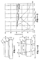
- the optically variable device 11 is comprised of a substrate 12 having a first surface 13 and a second surface 14.
- the substrate 12 should be formed of a transparent material.
- One material found to be satisfactory is a polymeric substrate formed, for example of polyethylene terephthalate.
- a symmetric three-layer coating 16 is carried by the first surface 13 of the substrate 12.
- the three-layer coating 16 is comprised of first and second absorber layers 17 and 18 with a dielectric spacer layer 19 disposed between the same.
- the first and second absorber layers 17 and 18 must be at least partially transmitting and preferably have a transmittance ranging from 20 to 50%.
- the dielectric layer 19 is transparent and serves as an optical spacer layer.
- the first and second absorber layers 17 and 18 it has been found that any one of a number of grey metals which have an n and k which are approximately equal can be utilized.
- chromium as well as nickel and palladium can be utilized.
- the grey metal layers can have a thickness ranging from 4.5 to 9.0 nanometers to provide a combined thickness for the first and second layers of 9.0 nanometers to 18 nanometers.
- the overall transmission may be as low as 12% whereas for the 9 nanometer combined thicknesses for the two layers, the transmission may be as high as approximately 30%.
- other absorbing materials than metal such as carbon or germanium, could also be used for layers 17 and 18.
- first and second absorber layers 17 and 18 have the same thickness. It should be appreciated that if desired the first and second absorber layers can have a different thickness.
- the bottom or second layer 18 can have a greater thickness than the first layer without substantially affecting color purity when used as an optically variable foil. If the first absorber layer 17 is made too thick, the color shift rapidly diminishes.
- the dielectric layer 19 can be formed of a suitable dielectric and preferably a dielectric having a low index of refraction such as magnesium fluoride having an index of refraction of 1.38. Materials having an index of refraction ranging from 1.2 to 1.65 can be used.
- the dielectric layer can have a thickness ranging from 150 nanometers to 950 nanometers.
- the top absorber layer 17 serves as a partial reflector and a partial transmitter.
- the bottom absorber layer 18 also serves as a partial reflector and a partial transmitter.
- the reflected portion of the light from the bottom layer 18 interferes with the reflected light coming from the front surface of the metal layer 17.
- This light interference provides color to the device.
- the specific color achieved is controlled by the thickness of the dielectric spacer layer 19. This spacer layer thickness controls the wavelength at which the light reflected from layer 17 interferes with light reflected from layer 18. For those wavelengths where the interference is destructive, a great portion of the light is absorbed in the device. For those wavelengths where the interference is constructive, most of the light not transmitted through the device is reflected.
- the relative intensities of the transmitted and reflected components are controlled by the thicknesses of layers 17, 18 and 19 and the optical properties of the material or materials chosen for layers 17, 18 and 19.
- the performance of the device can be understood by reference to Figure 2.
- the device For light coming in at relatively small angles relative to the normal, the device would have a green color. For light coming in at higher angles, it would have a blue color.
- an incident light beam 21 representing 100% of the visible light impinging on the device, a certain or first portion of the light represented by beam 22 will be absorbed within the device, a second portion 23 will be transmitted through the device, and a third portion represented by beam 24 will be reflected from the device.
- Beam 24 is comprised of light reflected from the outer surface of layer 17 and all the light reflected from internal surfaces of the device 11.
- the highest amplitude represented by reflectance of the beam component 24 is at wavelengths near 550 nanometers.
- the absorbed component represented by beam 22 is small compared to the reflected component represented by beam 24.
- the transmitted component represented by beam 23 is also higher at 550 nanometers than at other visible wavelengths.
- the absorbed component represented by beam 22 is large compared to the reflected component represented by beam 24.
- the transmitted component represented by beam 23 is lower than at wavelengths near 550 nanometers.
- the result of a high reflectance at 550 nanometers and low reflectances at 450 and 700 nanometers is the color green in reflection. Because the transmitted component represented by beam 23 is more intense at 550 nanometers than at 450 and 700 nanometers, the transmitted component will also appear green to some degree.
- a device made using a dielectric layer 19 of full wave optical thickness at 530 nanometers has a green color as described above. Reducing the full wave optical thickness of the dielectric layer 19 from 530 to 450 nanometers changes the normally incident reflected color from green to blue. Instead of a transparent optically variable green-to-blue device, there is provided a blue-to-magenta device. Conversely, increasing the full wave optical thickness of the dielectric spacer 19 from 530 to 650 nanometers results in a transparent optically variable magenta-to-green device.
- the device is symmetrical. This means that substantially the same optical effect is sobtained whether viewed from the direction of the top metal layer 17 or from the direction of the transparent substrate 12.
- a certain portion of the incident light represented by beam 21 will be transmitted through the device as a component represented by beam 23.
- a uniform reflective surface 26 such as a piece of white paper 27 is placed a short distance beneath the substrate 12 of the transparent optically variable device 11
- a light component represented by beam 31 is reflected off the surface 26 of the paper 27 and impinges on the surface 14 of the substrate 12.
- the component represented by beam 31 would be comprised of the reflected portion of light component represented by beam 23 and also the reflected portion of any stray light which reaches the paper surface 26 from other sources such as room lights.
- Component represented by beam 34 is comprised of light reflected from surface 14 and all light reflected from internal surfaces of the device 11.
- the component beam 33 reduces the purity of the color of reflected component beam 24.
- the white paper 27 can be replaced by a sheet of black paper which absorbs the incident light beam 23 and any stray light as well, thus eliminating the component beams 31, 32, 33 and 34.
- Such a device would provide a more pure color to component beam 24.
- the white paper 40 is replaced with a different reflective or partially reflective surface, the transmitted component beam 33 would be dependent on the properties of both the transparent optically variable device and the reflective surface 26.
- the device 11 can be bonded or laid directly onto a sheet of paper 27. Without an air gap between the surface 14 and the surface 26, the optical effect of the device 11 is changed.
- Component beam 31, representing 100% of the light incident on the backside of the device 11, is comprised only of that portion of light beam 23 which is reflected off the paper surface 26. Since there is no gap, there is also no opportunity for stray light to reflect off the paper surface 26.
- a white or silvery surface is the most efficient for reflecting component beam 23 and in turn results in the most intense re-transmitted component beam 33.
- a truly black surface eliminates component beam 31, and also component beams 32, 33 and 34. If a black surface is bonded to or is directly under the device 11 instead of a white surface 26, an increase in the color purity of component beam 24 results.
- the device can be made to reflect one color at normal angles of incidence, reflect a second color at higher angles, and transmit a third color.
- a green-to-blue shifting device transmits more blue light at 45° than at normal incidence.
- blue dyed PET for a substrate 12 transmits only blue light at all angles. Therefore producing a green-to-blue device on blue dyed PET substrate 12 results in a system which transmits significantly more light at 45° than at 0°.
- the blue light transmitted by the colored substrate is selectively absorbed by the green-to-blue shifting device and hence is not transmitted.
- informtion is printed on paper and held behind the aforementioned green-to-blue device on blue PET substrate, the information is only discernible at certain angles, as for example, 45°.
- optical variable device which is shown in Figures 1 and 2 provides a significant color shift with change of viewing angle as can be seen from Figure 3 where the performance is shown at 45° and 0° angles of incidence.
- the transparent optically variable device of the present invention can be utilized in various ways. For example, it can be incorporated with printing in the form of a logo or design. In such an application, the transparent optically variable device is placed between the viewer and the printed information.
- the visibility of the printing is affected by the transmittance of the device. For lower transmittance, the optically variable device appears brighter. However, the lower the transmittance the lower the visibility of the image behind the optically variable device.
- the optical variable device of the present invention can have many applications, as for example, in anti-counterfeiting.
- the image behind the optical device can be copied on conventional black and white and color copiers, the color shift cannot be copied because of the optical constraints of the copying machine.
- Dyes used in the toner of copying machines are insensitive to color change as the viewing angle is changed. Only an interference device as described in this invention allows color changes as the viewing angle is changed.
- the copier will only be able to faithfully reproduce the color of the device for the color at normal angles.
- the color copier will not copy the color of the device for any colors at non-normal angles.
- the copied image will present to the viewer only one color at all viewing angles; i.e., there will be no color shifting properties in the copy, whereas the original has color shifting properties as the viewing angle is changed.
- the optical variable device of the present invention utilizes a three-layer coating which is symmetric, the coating lends itself for use as pigments.
- the three-layer coating would be deposited on a substrate having a release coat thereon, after which it can be separated from the substrate and broken into particles.
Abstract
Description
- This invention relates to a transparent optically variable device.
- Optically variable devices are disclosed in U.S. Patents Nos. 4,705,300 and 4,705,356. Optically variable devices which can be used in optically variable inks and optically variable pigments are disclosed in application Serial No. 812,814 filed December 23, 1985, now abandoned in favor of application Serial No. 251,034 filed on September 26, 1988. However, those optically variable devices are opaque. There is a need for optically variable devices where some transparency can be obtained.
- In general, it is an object of the present invention to provide an optically variable device which has some degree of transparency.
- Another object of the invention is to provide an optically variable device of the above character which can be utilized in various different types of applications.
- Another object of the invention is to provide an optical variable device of the above character which has good color purity.
- Another object of the invention is to provide an optically variable device with as few as three layers making possible a lower cost device which can be manufactured on roll coating equipment.
- Another object of the invention is to provide an optical variable device of the above character which can be utilized in inks, as optically variable pigment.
- Additional objects and features of the invention will appear from the following description in which the preferred embodiments are set forth in detail in conjunction with the accompanying drawing.
- Figure 1 is a cross-sectional view of a transparent optically variable device incorporating the present invention.
- Figure 2 is a view showing the manner in which light is reflected from the optically variable device of the present invention which with angle shift provides a shift from one color to another.
- Figure 3 is a graph of reflectance of a transparent green-to-blue optically variable device incorporating the present invention.
- In general, it is an object of the present invention to provide a transparent optically variable device which is comprised of a transparent substrate having a first surface. A symmetric three-layer coating is disposed on the first surface. The symmetric three-layer coating is comprised of first and second partially transmitting absorber layers with a dielectric layer disposed between the first and second absorber layers. The absorber layers can be from 20 to 50% transmitting while still achieving color purity with color shift with angle.
- More particularly as shown in the drawings, the optically variable device 11 is comprised of a
substrate 12 having afirst surface 13 and asecond surface 14. In accordance with the present invention thesubstrate 12 should be formed of a transparent material. One material found to be satisfactory is a polymeric substrate formed, for example of polyethylene terephthalate. A symmetric three-layer coating 16 is carried by thefirst surface 13 of thesubstrate 12. The three-layer coating 16 is comprised of first andsecond absorber layers dielectric spacer layer 19 disposed between the same. The first andsecond absorber layers dielectric layer 19 is transparent and serves as an optical spacer layer. - For the first and
second absorber layers layers - In conjunction with the foregoing it has been assumed that the first and
second absorber layers second layer 18 can have a greater thickness than the first layer without substantially affecting color purity when used as an optically variable foil. If thefirst absorber layer 17 is made too thick, the color shift rapidly diminishes. - The
dielectric layer 19 can be formed of a suitable dielectric and preferably a dielectric having a low index of refraction such as magnesium fluoride having an index of refraction of 1.38. Materials having an index of refraction ranging from 1.2 to 1.65 can be used. The dielectric layer can have a thickness ranging from 150 nanometers to 950 nanometers. - The
top absorber layer 17 serves as a partial reflector and a partial transmitter. Thebottom absorber layer 18 also serves as a partial reflector and a partial transmitter. The reflected portion of the light from thebottom layer 18 interferes with the reflected light coming from the front surface of themetal layer 17. This light interference provides color to the device. The specific color achieved is controlled by the thickness of thedielectric spacer layer 19. This spacer layer thickness controls the wavelength at which the light reflected fromlayer 17 interferes with light reflected fromlayer 18. For those wavelengths where the interference is destructive, a great portion of the light is absorbed in the device. For those wavelengths where the interference is constructive, most of the light not transmitted through the device is reflected. It is the combination of high reflectances at some wavelengths and low reflectances at other wavelengths that gives the device its color. The relative intensities of the transmitted and reflected components are controlled by the thicknesses oflayers layers - Assuming that a green-to-blue transparent optically variable device 11 is to be provided, the performance of the device can be understood by reference to Figure 2. For light coming in at relatively small angles relative to the normal, the device would have a green color. For light coming in at higher angles, it would have a blue color. Referring to Figure 2, for an
incident light beam 21 representing 100% of the visible light impinging on the device, a certain or first portion of the light represented bybeam 22 will be absorbed within the device, asecond portion 23 will be transmitted through the device, and a third portion represented bybeam 24 will be reflected from the device.Beam 24 is comprised of light reflected from the outer surface oflayer 17 and all the light reflected from internal surfaces of the device 11. - For the green-to-blue transparent optically variable device 11 of the current example, at normal incidence the highest amplitude represented by reflectance of the
beam component 24 is at wavelengths near 550 nanometers. At these wavelengths near 550 nanometers, the absorbed component represented bybeam 22 is small compared to the reflected component represented bybeam 24. The transmitted component represented bybeam 23 is also higher at 550 nanometers than at other visible wavelengths. At the same time, at wavelengths near 450 and 700 nanometers the absorbed component represented bybeam 22 is large compared to the reflected component represented bybeam 24. At wavelengths near 450 and 700 nanometers the transmitted component represented bybeam 23 is lower than at wavelengths near 550 nanometers. The result of a high reflectance at 550 nanometers and low reflectances at 450 and 700 nanometers is the color green in reflection. Because the transmitted component represented bybeam 23 is more intense at 550 nanometers than at 450 and 700 nanometers, the transmitted component will also appear green to some degree. - Changing the thickness of the
dielectric spacer 19 while holding the metal thicknesses oflayers dielectric layer 19 of full wave optical thickness at 530 nanometers has a green color as described above. Reducing the full wave optical thickness of thedielectric layer 19 from 530 to 450 nanometers changes the normally incident reflected color from green to blue. Instead of a transparent optically variable green-to-blue device, there is provided a blue-to-magenta device. Conversely, increasing the full wave optical thickness of thedielectric spacer 19 from 530 to 650 nanometers results in a transparent optically variable magenta-to-green device. Other colors and color shifts in addition to those mentioned above can be produced by varying the full wave optical thickness of the dielectric spacer between the limits of 150 and 950 nanometers. At full wave optical thicknesses below 150 nanometers, the device appears brown or black with no apparent angle shift. At full wave optical thicknesses above 950 nanometers, the color purity is reduced to a point that the device does not function properly. - It should be realized that if the two metal layers are made of the same material and coated to the same thickness, the device is symmetrical. This means that substantially the same optical effect is sobtained whether viewed from the direction of the
top metal layer 17 or from the direction of thetransparent substrate 12. - When viewing the device from the direction or side of the
top metal layer 17, it can be seen that a certain portion of the incident light represented bybeam 21 will be transmitted through the device as a component represented bybeam 23. When a uniformreflective surface 26 such as a piece ofwhite paper 27 is placed a short distance beneath thesubstrate 12 of the transparent optically variable device 11, a light component represented bybeam 31 is reflected off thesurface 26 of thepaper 27 and impinges on thesurface 14 of thesubstrate 12. The component represented bybeam 31 would be comprised of the reflected portion of light component represented bybeam 23 and also the reflected portion of any stray light which reaches thepaper surface 26 from other sources such as room lights. - Referring to Figure 2, for an
incident light beam 31 representing 100% of the visible light impinging on the backside of the device, a certain portion of the light represented bybeam 33 will be transmitted back through the device, a second portion represented bybeam 32 will be absorbed within the device, and a third portion represented bybeam 34 will be reflected from the device back toward thepaper surface 26 and thus is unavailable to the viewer above. Component represented bybeam 34 is comprised of light reflected fromsurface 14 and all light reflected from internal surfaces of the device 11. Thecomponent beam 33 reduces the purity of the color of reflectedcomponent beam 24. When this reduced color purity is undesirable, thewhite paper 27 can be replaced by a sheet of black paper which absorbs theincident light beam 23 and any stray light as well, thus eliminating the component beams 31, 32, 33 and 34. Such a device would provide a more pure color tocomponent beam 24. When thewhite paper 40 is replaced with a different reflective or partially reflective surface, the transmittedcomponent beam 33 would be dependent on the properties of both the transparent optically variable device and thereflective surface 26. - Alternatively, rather than positioning the device 11 above a piece of paper, the device 11 can be bonded or laid directly onto a sheet of
paper 27. Without an air gap between thesurface 14 and thesurface 26, the optical effect of the device 11 is changed.Component beam 31, representing 100% of the light incident on the backside of the device 11, is comprised only of that portion oflight beam 23 which is reflected off thepaper surface 26. Since there is no gap, there is also no opportunity for stray light to reflect off thepaper surface 26. A white or silvery surface is the most efficient for reflectingcomponent beam 23 and in turn results in the most intensere-transmitted component beam 33. A truly black surface eliminatescomponent beam 31, and also component beams 32, 33 and 34. If a black surface is bonded to or is directly under the device 11 instead of awhite surface 26, an increase in the color purity ofcomponent beam 24 results. - Novel effects in addition to those described above can be achieved through the use of colored transparent substrates. For example, the device can be made to reflect one color at normal angles of incidence, reflect a second color at higher angles, and transmit a third color. In another example, a green-to-blue shifting device transmits more blue light at 45° than at normal incidence. At the same time, blue dyed PET for a
substrate 12 transmits only blue light at all angles. Therefore producing a green-to-blue device on bluedyed PET substrate 12 results in a system which transmits significantly more light at 45° than at 0°. At incident angles near normal, the blue light transmitted by the colored substrate is selectively absorbed by the green-to-blue shifting device and hence is not transmitted. When informtion is printed on paper and held behind the aforementioned green-to-blue device on blue PET substrate, the information is only discernible at certain angles, as for example, 45°. - It can be seen that the optical variable device which is shown in Figures 1 and 2 provides a significant color shift with change of viewing angle as can be seen from Figure 3 where the performance is shown at 45° and 0° angles of incidence. In addition, it is possible to achieve at least partial transmittance with only a small sacrifice in purity of the colors.
- It should be appreciated that the transparent optically variable device of the present invention can be utilized in various ways. For example, it can be incorporated with printing in the form of a logo or design. In such an application, the transparent optically variable device is placed between the viewer and the printed information.
- Since the viewer sees the printed information through the optically variable device, the visibility of the printing is affected by the transmittance of the device. For lower transmittance, the optically variable device appears brighter. However, the lower the transmittance the lower the visibility of the image behind the optically variable device.
- The optical variable device of the present invention can have many applications, as for example, in anti-counterfeiting. Although the image behind the optical device can be copied on conventional black and white and color copiers, the color shift cannot be copied because of the optical constraints of the copying machine. Dyes used in the toner of copying machines are insensitive to color change as the viewing angle is changed. Only an interference device as described in this invention allows color changes as the viewing angle is changed. The copier will only be able to faithfully reproduce the color of the device for the color at normal angles. The color copier will not copy the color of the device for any colors at non-normal angles. Thus, the copied image will present to the viewer only one color at all viewing angles; i.e., there will be no color shifting properties in the copy, whereas the original has color shifting properties as the viewing angle is changed.
- Since the optical variable device of the present invention utilizes a three-layer coating which is symmetric, the coating lends itself for use as pigments. In such applications, the three-layer coating would be deposited on a substrate having a release coat thereon, after which it can be separated from the substrate and broken into particles.
- Sizing these symmetrical particles allows one to form optically variable pigments for use in ink vehicles as well as other applications as in described in U.S Patent No. 4,705,356 and in pending application Serial No. 251,034.
Claims (10)
Applications Claiming Priority (2)
| Application Number | Priority Date | Filing Date | Title |
|---|---|---|---|
| US07/343,893 US5278590A (en) | 1989-04-26 | 1989-04-26 | Transparent optically variable device |
| US343893 | 1989-04-26 |
Publications (3)
| Publication Number | Publication Date |
|---|---|
| EP0395410A2 true EP0395410A2 (en) | 1990-10-31 |
| EP0395410A3 EP0395410A3 (en) | 1991-02-27 |
| EP0395410B1 EP0395410B1 (en) | 1997-08-13 |
Family
ID=23348127
Family Applications (1)
| Application Number | Title | Priority Date | Filing Date |
|---|---|---|---|
| EP90304531A Expired - Lifetime EP0395410B1 (en) | 1989-04-26 | 1990-04-26 | Transparent optically variable device |
Country Status (10)
| Country | Link |
|---|---|
| US (1) | US5278590A (en) |
| EP (1) | EP0395410B1 (en) |
| JP (1) | JP2831095B2 (en) |
| AT (1) | ATE156916T1 (en) |
| CA (1) | CA2015301C (en) |
| DE (1) | DE69031240T2 (en) |
| DK (1) | DK0395410T3 (en) |
| ES (1) | ES2104582T3 (en) |
| GR (1) | GR3024543T3 (en) |
| HK (1) | HK1002042A1 (en) |
Cited By (19)
| Publication number | Priority date | Publication date | Assignee | Title |
|---|---|---|---|---|
| WO2002000446A1 (en) * | 2000-06-28 | 2002-01-03 | De La Rue International Limited | A security device |
| WO2002024818A1 (en) * | 2000-09-22 | 2002-03-28 | Flex Products, Inc. | Optically variable pigments and foils with enhanced color shifting properties |
| US6849343B2 (en) | 2000-10-10 | 2005-02-01 | Flex Products, Inc. | Titanium-containing interference pigments and foils with color shifting properties |
| WO2005038136A1 (en) * | 2003-10-17 | 2005-04-28 | Giesecke & Devrient Gmbh | Security element with a color-shift effect |
| WO2006002756A2 (en) * | 2004-07-05 | 2006-01-12 | Giesecke & Devrient Gmbh | Security element with a color shift tilt effect |
| WO2010003646A1 (en) * | 2008-07-09 | 2010-01-14 | Giesecke & Devrient Gmbh | Security element |
| DE102008049631A1 (en) | 2008-09-30 | 2010-04-01 | Giesecke & Devrient Gmbh | Card with embedded security feature |
| WO2011010041A2 (en) | 2009-07-20 | 2011-01-27 | L'oreal | Emulsion containing a bismuth oxychloride dispersion |
| US7923097B2 (en) | 2003-08-12 | 2011-04-12 | Giesecke & Devrient Gmbh | Security element with thin-layer element |
| WO2011067807A1 (en) | 2009-12-02 | 2011-06-09 | L'oreal | Cosmetic composition containing fusiform particles for cosmetic use |
| WO2012001808A1 (en) | 2010-07-01 | 2012-01-05 | トヨタ自動車株式会社 | Method for producing ceramic laminate, and ceramic laminate produced by the production method |
| WO2012042570A1 (en) | 2010-09-29 | 2012-04-05 | L'oreal | A cosmetic method for hiding skin imperfections |
| US20120270020A1 (en) * | 2011-04-21 | 2012-10-25 | Sigma Laboratories Of Arizona, Llc. | Polymer-based optically variable devices |
| RU2466874C2 (en) * | 2007-05-21 | 2012-11-20 | Овд Кинеграм Аг | Multilayer body |
| WO2014203913A1 (en) | 2013-06-18 | 2014-12-24 | L'oreal | Cosmetic composition |
| US9274258B2 (en) | 2009-09-15 | 2016-03-01 | Giesecke & Devrient Gmbh | Thin-layer element having an interference layer structure |
| WO2017013394A1 (en) * | 2015-07-22 | 2017-01-26 | Isis Innovation Limited | Optical device |
| US10562333B2 (en) | 2012-01-12 | 2020-02-18 | Viavi Solutions Inc. | Article with curved patterns formed of aligned pigment flakes |
| US11230127B2 (en) | 2002-07-15 | 2022-01-25 | Viavi Solutions Inc. | Method and apparatus for orienting magnetic flakes |
Families Citing this family (83)
| Publication number | Priority date | Publication date | Assignee | Title |
|---|---|---|---|---|
| US5865471A (en) | 1993-08-05 | 1999-02-02 | Kimberly-Clark Worldwide, Inc. | Photo-erasable data processing forms |
| US5877895A (en) * | 1995-03-20 | 1999-03-02 | Catalina Coatings, Inc. | Multicolor interference coating |
| US6156325A (en) * | 1998-09-16 | 2000-12-05 | L'oreal | Nail enamel composition containing a urea-modified thixotropic agent |
| DE19844357C2 (en) | 1998-09-28 | 2001-04-05 | Hilmar Weinert | Belt steaming system and process for the production of plane-parallel platelets |
| US6157489A (en) * | 1998-11-24 | 2000-12-05 | Flex Products, Inc. | Color shifting thin film pigments |
| US6150022A (en) * | 1998-12-07 | 2000-11-21 | Flex Products, Inc. | Bright metal flake based pigments |
| US20070195392A1 (en) * | 1999-07-08 | 2007-08-23 | Jds Uniphase Corporation | Adhesive Chromagram And Method Of Forming Thereof |
| US7047883B2 (en) | 2002-07-15 | 2006-05-23 | Jds Uniphase Corporation | Method and apparatus for orienting magnetic flakes |
| US7667895B2 (en) * | 1999-07-08 | 2010-02-23 | Jds Uniphase Corporation | Patterned structures with optically variable effects |
| US6761959B1 (en) * | 1999-07-08 | 2004-07-13 | Flex Products, Inc. | Diffractive surfaces with color shifting backgrounds |
| US6987590B2 (en) * | 2003-09-18 | 2006-01-17 | Jds Uniphase Corporation | Patterned reflective optical structures |
| US6241858B1 (en) | 1999-09-03 | 2001-06-05 | Flex Products, Inc. | Methods and apparatus for producing enhanced interference pigments |
| US6524381B1 (en) | 2000-03-31 | 2003-02-25 | Flex Products, Inc. | Methods for producing enhanced interference pigments |
| US6545809B1 (en) | 1999-10-20 | 2003-04-08 | Flex Products, Inc. | Color shifting carbon-containing interference pigments |
| AU2005200844B2 (en) * | 2000-01-21 | 2006-04-06 | Viavi Solutions Inc. | Optically variable security devices |
| EP1849620B1 (en) * | 2000-01-21 | 2016-03-23 | Viavi Solutions Inc. | Optically variable security devices |
| US11768321B2 (en) | 2000-01-21 | 2023-09-26 | Viavi Solutions Inc. | Optically variable security devices |
| US6586098B1 (en) | 2000-07-27 | 2003-07-01 | Flex Products, Inc. | Composite reflective flake based pigments comprising reflector layers on bothside of a support layer |
| US6416872B1 (en) | 2000-08-30 | 2002-07-09 | Cp Films, Inc. | Heat reflecting film with low visible reflectance |
| US6565770B1 (en) | 2000-11-17 | 2003-05-20 | Flex Products, Inc. | Color-shifting pigments and foils with luminescent coatings |
| US6572784B1 (en) | 2000-11-17 | 2003-06-03 | Flex Products, Inc. | Luminescent pigments and foils with color-shifting properties |
| US6555096B2 (en) | 2000-12-04 | 2003-04-29 | L'oreal S.A. | Nail enamel composition containing a urea-modified thixotropic agent in a solvent system |
| DE10064616C2 (en) | 2000-12-22 | 2003-02-06 | Ovd Kinegram Ag Zug | Decorative film and method for labeling the decorative film |
| US20020160194A1 (en) | 2001-04-27 | 2002-10-31 | Flex Products, Inc. | Multi-layered magnetic pigments and foils |
| US6808806B2 (en) * | 2001-05-07 | 2004-10-26 | Flex Products, Inc. | Methods for producing imaged coated articles by using magnetic pigments |
| US7625632B2 (en) * | 2002-07-15 | 2009-12-01 | Jds Uniphase Corporation | Alignable diffractive pigment flakes and method and apparatus for alignment and images formed therefrom |
| US6841238B2 (en) | 2002-04-05 | 2005-01-11 | Flex Products, Inc. | Chromatic diffractive pigments and foils |
| US6692830B2 (en) * | 2001-07-31 | 2004-02-17 | Flex Products, Inc. | Diffractive pigment flakes and compositions |
| US20050169950A1 (en) * | 2002-01-08 | 2005-08-04 | Marie-Laure Delacour | Solid cosmetic composition comprising fibers |
| DE10202035B4 (en) | 2002-01-18 | 2018-10-18 | Giesecke+Devrient Currency Technology Gmbh | Security element with color shift effect and magnetic properties, article with such a security element and method for producing the security element and the article. |
| US20030146044A1 (en) * | 2002-02-01 | 2003-08-07 | Jordan Omar P. | Sefety harness with support strap |
| DE10206357A1 (en) | 2002-02-14 | 2003-08-28 | Giesecke & Devrient Gmbh | Security element and security document with such a security element |
| US6997981B1 (en) * | 2002-05-20 | 2006-02-14 | Jds Uniphase Corporation | Thermal control interface coatings and pigments |
| US20100208351A1 (en) * | 2002-07-15 | 2010-08-19 | Nofi Michael R | Selective and oriented assembly of platelet materials and functional additives |
| US7934451B2 (en) * | 2002-07-15 | 2011-05-03 | Jds Uniphase Corporation | Apparatus for orienting magnetic flakes |
| AT413360B (en) | 2002-08-06 | 2006-02-15 | Hueck Folien Gmbh | METHOD FOR PRODUCING FAKE-SECURE IDENTIFICATION FEATURES |
| US6970236B1 (en) | 2002-08-19 | 2005-11-29 | Jds Uniphase Corporation | Methods and systems for verification of interference devices |
| US9458324B2 (en) | 2002-09-13 | 2016-10-04 | Viava Solutions Inc. | Flakes with undulate borders and method of forming thereof |
| US7645510B2 (en) * | 2002-09-13 | 2010-01-12 | Jds Uniphase Corporation | Provision of frames or borders around opaque flakes for covert security applications |
| US7674501B2 (en) * | 2002-09-13 | 2010-03-09 | Jds Uniphase Corporation | Two-step method of coating an article for security printing by application of electric or magnetic field |
| US8025952B2 (en) | 2002-09-13 | 2011-09-27 | Jds Uniphase Corporation | Printed magnetic ink overt security image |
| US9164575B2 (en) * | 2002-09-13 | 2015-10-20 | Jds Uniphase Corporation | Provision of frames or borders around pigment flakes for covert security applications |
| ATE461635T1 (en) * | 2002-12-19 | 2010-04-15 | Rapid Intervention Technologie | FULL BODY HARNESS |
| US7979919B2 (en) * | 2002-12-19 | 2011-07-19 | Rapid Intervention Technologies, Inc. | Full body harness |
| US20060195962A1 (en) * | 2002-12-19 | 2006-09-07 | Rit Rescue And Escape Systems | Full body harness |
| US7169472B2 (en) | 2003-02-13 | 2007-01-30 | Jds Uniphase Corporation | Robust multilayer magnetic pigments and foils |
| EP1625395B1 (en) * | 2003-05-14 | 2009-09-16 | InDex Pharmaceuticals AB | Method for identifying tff2 regulating agents |
| US20080019003A1 (en) * | 2003-07-14 | 2008-01-24 | Jds Uniphase Corporation | Vacuum Roll Coated Security Thin Film Interference Products With Overt And/Or Covert Patterned Layers |
| CN101164797B (en) * | 2003-07-14 | 2012-07-18 | Jds尤尼费斯公司 | Security thread |
| DE10334310A1 (en) | 2003-07-28 | 2005-02-24 | Giesecke & Devrient Gmbh | Security paper for the production of value documents |
| US7550197B2 (en) * | 2003-08-14 | 2009-06-23 | Jds Uniphase Corporation | Non-toxic flakes for authentication of pharmaceutical articles |
| CN1294230C (en) * | 2003-12-11 | 2007-01-10 | 同济大学 | Composite photochromic polyaminoester material and preparation method thereof |
| US20050175562A1 (en) * | 2004-01-05 | 2005-08-11 | Anke Hadasch | Skin makeup composition |
| AT504587A1 (en) | 2004-02-16 | 2008-06-15 | Hueck Folien Gmbh | IMPACT-SAFE SAFETY FEATURE WITH COLOR TIP EFFECT |
| US20070190298A1 (en) * | 2005-01-14 | 2007-08-16 | Cabot Corporation | Security features, their use and processes for making them |
| CA2537732A1 (en) * | 2005-04-06 | 2006-10-06 | Jds Uniphase Corporation | High chroma optically variable colour-shifting glitter |
| CA2541568C (en) | 2005-04-06 | 2014-05-13 | Jds Uniphase Corporation | Dynamic appearance-changing optical devices (dacod) printed in a shaped magnetic field including printable fresnel structures |
| EP1719636A1 (en) * | 2005-05-04 | 2006-11-08 | Sicpa Holding S.A. | Black-to-color shifting security element |
| AU2006202315B2 (en) * | 2005-06-17 | 2011-01-27 | Viavi Solutions Inc. | Covert security coating |
| CA2564764C (en) * | 2005-10-25 | 2014-05-13 | Jds Uniphase Corporation | Patterned optical structures with enhanced security feature |
| CA2570965A1 (en) * | 2005-12-15 | 2007-06-15 | Jds Uniphase Corporation | Security device with metameric features using diffractive pigment flakes |
| JP4933150B2 (en) * | 2006-05-23 | 2012-05-16 | 株式会社大裕商事 | Insole of women's shoes with a high heel |
| US8070186B2 (en) * | 2006-05-31 | 2011-12-06 | Cabot Corporation | Printable reflective features formed from multiple inks and processes for making them |
| US8790459B2 (en) * | 2006-05-31 | 2014-07-29 | Cabot Corporation | Colored reflective features and inks and processes for making them |
| US20070279718A1 (en) * | 2006-05-31 | 2007-12-06 | Cabot Corporation | Reflective features with co-planar elements and processes for making them |
| US9533523B2 (en) | 2006-05-31 | 2017-01-03 | Sicpa Holding Sa | Reflective features with co-planar elements and processes for making them |
| US20070281136A1 (en) * | 2006-05-31 | 2007-12-06 | Cabot Corporation | Ink jet printed reflective features and processes and inks for making them |
| TWI437059B (en) * | 2006-07-12 | 2014-05-11 | Jds Uniphase Corp | Stamping a coating of cured field aligned special effect flakes and image formed thereby |
| US7829162B2 (en) * | 2006-08-29 | 2010-11-09 | international imagining materials, inc | Thermal transfer ribbon |
| DE102007034716A1 (en) | 2007-07-23 | 2009-01-29 | Giesecke & Devrient Gmbh | security element |
| JP5478493B2 (en) * | 2007-09-17 | 2014-04-23 | クォルコム・メムズ・テクノロジーズ・インコーポレーテッド | Translucent / semi-transmissive light emitting interference device |
| JP2009193069A (en) | 2008-02-13 | 2009-08-27 | Jds Uniphase Corp | Medium for laser printing including optical special effect flake |
| EP3236299A1 (en) | 2008-09-05 | 2017-10-25 | Viavi Solutions Inc. | An optical device exhibiting color shift upon rotation |
| WO2013022699A1 (en) | 2011-08-05 | 2013-02-14 | Technical Graphics, Inc. | A method for producing complex color shifting effects |
| DE102012018434A1 (en) * | 2012-09-18 | 2014-03-20 | Giesecke & Devrient Gmbh | Optically variable security element with additional open / see-through effect |
| US9482800B2 (en) | 2013-06-10 | 2016-11-01 | Viavi Solutions Inc. | Durable optical interference pigment with a bimetal core |
| AT517320B1 (en) | 2015-05-29 | 2020-04-15 | Hueck Folien Gmbh | Security element with color shift effect |
| GB2542786B (en) * | 2015-09-29 | 2018-02-28 | De La Rue Int Ltd | Security print media and method of manufacture thereof |
| TW201922475A (en) | 2017-10-05 | 2019-06-16 | 美商偉福夫特科技公司 | Optical structures providing dichroic effects |
| CN113165964B (en) | 2018-09-28 | 2023-04-07 | 康宁股份有限公司 | High hardness article comprising an optical layer and method of making the same |
| CA3132715A1 (en) | 2019-04-04 | 2020-10-08 | Wavefront Technology, Inc. | Optical structures providing dichroic effects |
| CN110780371B (en) * | 2019-09-29 | 2021-12-28 | 惠州市华阳光学技术有限公司 | All-dielectric small-angle dependent pigment flakes |
| EP4154314A1 (en) | 2020-05-18 | 2023-03-29 | University of Rochester | Multispectral imaging cmos sensor |
Citations (4)
| Publication number | Priority date | Publication date | Assignee | Title |
|---|---|---|---|---|
| DE716153C (en) * | 1939-12-08 | 1942-01-14 | Jenaer Glaswerk Schott & Gen | Interference light filter |
| US3858977A (en) * | 1972-01-18 | 1975-01-07 | Canadian Patents Dev | Optical interference authenticating means |
| US4705300A (en) * | 1984-07-13 | 1987-11-10 | Optical Coating Laboratory, Inc. | Thin film optically variable article and method having gold to green color shift for currency authentication |
| US4705356A (en) * | 1984-07-13 | 1987-11-10 | Optical Coating Laboratory, Inc. | Thin film optical variable article having substantial color shift with angle and method |
Family Cites Families (6)
| Publication number | Priority date | Publication date | Assignee | Title |
|---|---|---|---|---|
| US4048039A (en) * | 1975-03-07 | 1977-09-13 | Balzers Patent Und Beteiligungs-Ag | Method of producing a light transmitting absorbing coating on substrates |
| JPS5647012A (en) * | 1979-09-26 | 1981-04-28 | Nippon Hoso Kyokai <Nhk> | Fabry-perot etalon |
| EP0098088B1 (en) * | 1982-06-30 | 1987-03-11 | Teijin Limited | Optical laminar structure |
| JPS5952641A (en) * | 1982-07-20 | 1984-03-27 | 帝人株式会社 | Laminated intermediate membrane |
| US4721217A (en) * | 1986-08-07 | 1988-01-26 | Optical Coating Laboratory, Inc. | Tamper evident optically variable device and article utilizing the same |
| DE3825702A1 (en) * | 1988-07-28 | 1990-02-01 | Michael Huber Muenchen Gmbh Fa | GONIOCHROMATIC PIGMENTS, METHOD FOR THE PRODUCTION THEREOF AND THEIR USE FOR THE PRODUCTION OF SAFETY AND EFFECT COLORS |
-
1989
- 1989-04-26 US US07/343,893 patent/US5278590A/en not_active Expired - Lifetime
-
1990
- 1990-04-24 CA CA002015301A patent/CA2015301C/en not_active Expired - Lifetime
- 1990-04-26 DK DK90304531.8T patent/DK0395410T3/en active
- 1990-04-26 DE DE69031240T patent/DE69031240T2/en not_active Expired - Lifetime
- 1990-04-26 ES ES90304531T patent/ES2104582T3/en not_active Expired - Lifetime
- 1990-04-26 JP JP2111600A patent/JP2831095B2/en not_active Expired - Fee Related
- 1990-04-26 EP EP90304531A patent/EP0395410B1/en not_active Expired - Lifetime
- 1990-04-26 AT AT90304531T patent/ATE156916T1/en not_active IP Right Cessation
-
1997
- 1997-08-26 GR GR970402183T patent/GR3024543T3/en unknown
-
1998
- 1998-02-11 HK HK98101052A patent/HK1002042A1/en not_active IP Right Cessation
Patent Citations (4)
| Publication number | Priority date | Publication date | Assignee | Title |
|---|---|---|---|---|
| DE716153C (en) * | 1939-12-08 | 1942-01-14 | Jenaer Glaswerk Schott & Gen | Interference light filter |
| US3858977A (en) * | 1972-01-18 | 1975-01-07 | Canadian Patents Dev | Optical interference authenticating means |
| US4705300A (en) * | 1984-07-13 | 1987-11-10 | Optical Coating Laboratory, Inc. | Thin film optically variable article and method having gold to green color shift for currency authentication |
| US4705356A (en) * | 1984-07-13 | 1987-11-10 | Optical Coating Laboratory, Inc. | Thin film optical variable article having substantial color shift with angle and method |
Non-Patent Citations (1)
| Title |
|---|
| J. FLUEGGE: "STUDIENBUCH ZUR TECHNISCHEN OPTIK" 1976, Vandenhoek & Ruprecht, Göttingen, DE * |
Cited By (36)
| Publication number | Priority date | Publication date | Assignee | Title |
|---|---|---|---|---|
| CZ298880B6 (en) * | 2000-06-28 | 2008-03-05 | De La Rue International Limited | Security device |
| US6903850B2 (en) | 2000-06-28 | 2005-06-07 | De La Rue International Limited | Security device |
| WO2002000446A1 (en) * | 2000-06-28 | 2002-01-03 | De La Rue International Limited | A security device |
| AU2001266211B2 (en) * | 2000-06-28 | 2004-03-04 | De La Rue International Limited | A security device |
| WO2002024818A1 (en) * | 2000-09-22 | 2002-03-28 | Flex Products, Inc. | Optically variable pigments and foils with enhanced color shifting properties |
| US6933048B2 (en) | 2000-10-10 | 2005-08-23 | Jds Uniphase Corporation | Titanium-containing interference pigments and foils with color shifting properties |
| US6991860B2 (en) | 2000-10-10 | 2006-01-31 | Jds Uniphase Corporation | Titanium-containing interference pigments and foils with color shifting properties |
| US6849343B2 (en) | 2000-10-10 | 2005-02-01 | Flex Products, Inc. | Titanium-containing interference pigments and foils with color shifting properties |
| US11230127B2 (en) | 2002-07-15 | 2022-01-25 | Viavi Solutions Inc. | Method and apparatus for orienting magnetic flakes |
| US7923097B2 (en) | 2003-08-12 | 2011-04-12 | Giesecke & Devrient Gmbh | Security element with thin-layer element |
| WO2005038136A1 (en) * | 2003-10-17 | 2005-04-28 | Giesecke & Devrient Gmbh | Security element with a color-shift effect |
| WO2006002756A3 (en) * | 2004-07-05 | 2006-08-10 | Giesecke & Devrient Gmbh | Security element with a color shift tilt effect |
| WO2006002756A2 (en) * | 2004-07-05 | 2006-01-12 | Giesecke & Devrient Gmbh | Security element with a color shift tilt effect |
| US8432589B2 (en) | 2007-05-21 | 2013-04-30 | Ovd Kinegram Ag | Multi-layer body having optical-action elements for producing an optical effect |
| RU2466874C2 (en) * | 2007-05-21 | 2012-11-20 | Овд Кинеграм Аг | Multilayer body |
| WO2010003646A1 (en) * | 2008-07-09 | 2010-01-14 | Giesecke & Devrient Gmbh | Security element |
| CN102089123A (en) * | 2008-07-09 | 2011-06-08 | 德国捷德有限公司 | Security element |
| CN102089123B (en) * | 2008-07-09 | 2014-03-19 | 德国捷德有限公司 | Security element |
| US8490879B2 (en) | 2008-07-09 | 2013-07-23 | Giesecke & Devrient Gmbh | Security element |
| DE102008049631A1 (en) | 2008-09-30 | 2010-04-01 | Giesecke & Devrient Gmbh | Card with embedded security feature |
| US8403230B2 (en) | 2008-09-30 | 2013-03-26 | Giesecke & Devrient Gmbh | Card having embedded security element |
| EP2826460A1 (en) | 2009-07-20 | 2015-01-21 | L'oreal | Emulsion containing a dispersion of bismuth oxychloride |
| EP2826459A1 (en) | 2009-07-20 | 2015-01-21 | L'oreal | Emulsion containing a dispersion of bismuth oxychloride |
| WO2011010041A2 (en) | 2009-07-20 | 2011-01-27 | L'oreal | Emulsion containing a bismuth oxychloride dispersion |
| US9274258B2 (en) | 2009-09-15 | 2016-03-01 | Giesecke & Devrient Gmbh | Thin-layer element having an interference layer structure |
| WO2011067807A1 (en) | 2009-12-02 | 2011-06-09 | L'oreal | Cosmetic composition containing fusiform particles for cosmetic use |
| WO2012001808A1 (en) | 2010-07-01 | 2012-01-05 | トヨタ自動車株式会社 | Method for producing ceramic laminate, and ceramic laminate produced by the production method |
| WO2012042570A1 (en) | 2010-09-29 | 2012-04-05 | L'oreal | A cosmetic method for hiding skin imperfections |
| US8815337B2 (en) * | 2011-04-21 | 2014-08-26 | Sigma Laboratories Of Arizona, Llc | Methods for fabrication of polymer-based optically variable devices |
| US20120270020A1 (en) * | 2011-04-21 | 2012-10-25 | Sigma Laboratories Of Arizona, Llc. | Polymer-based optically variable devices |
| US10562333B2 (en) | 2012-01-12 | 2020-02-18 | Viavi Solutions Inc. | Article with curved patterns formed of aligned pigment flakes |
| US10752042B2 (en) | 2012-01-12 | 2020-08-25 | Viavi Solutions Inc. | Article with dynamic frame formed with aligned pigment flakes |
| US11198315B2 (en) | 2012-01-12 | 2021-12-14 | Viavi Solutions Inc. | Article with curved patterns formed of aligned pigment flakes |
| WO2014203913A1 (en) | 2013-06-18 | 2014-12-24 | L'oreal | Cosmetic composition |
| WO2017013394A1 (en) * | 2015-07-22 | 2017-01-26 | Isis Innovation Limited | Optical device |
| US10317707B2 (en) | 2015-07-22 | 2019-06-11 | Oxford University Innovation Limited | Optical device |
Also Published As
| Publication number | Publication date |
|---|---|
| JP2831095B2 (en) | 1998-12-02 |
| EP0395410A3 (en) | 1991-02-27 |
| CA2015301A1 (en) | 1990-10-26 |
| CA2015301C (en) | 1999-09-21 |
| DE69031240T2 (en) | 1997-12-04 |
| DK0395410T3 (en) | 1998-03-30 |
| DE69031240D1 (en) | 1997-09-18 |
| ATE156916T1 (en) | 1997-08-15 |
| EP0395410B1 (en) | 1997-08-13 |
| HK1002042A1 (en) | 1998-07-24 |
| ES2104582T3 (en) | 1997-10-16 |
| JPH03129303A (en) | 1991-06-03 |
| GR3024543T3 (en) | 1997-12-31 |
| US5278590A (en) | 1994-01-11 |
Similar Documents
| Publication | Publication Date | Title |
|---|---|---|
| US5278590A (en) | Transparent optically variable device | |
| US7145723B2 (en) | Security element | |
| US5624731A (en) | Multi-color, multi-image retroflective goniochromatic display | |
| KR100441995B1 (en) | Paired optically variable device with optically variable pigments | |
| US4417784A (en) | Multiple image encoding using surface relief structures as authenticating device for sheet-material authenticated item | |
| US5830609A (en) | Security printed document to prevent unauthorized copying | |
| US6171734B1 (en) | Security printed document to prevent unauthorized copying | |
| US20030179364A1 (en) | Micro-optics for article identification | |
| JPH01155381A (en) | Recording preparation | |
| JP2724148B2 (en) | Anti-photocopy and anti-telefacsimile paper | |
| JPH0664206B2 (en) | Directional imaged sheet | |
| JPH0350586A (en) | Electrophotographic copied image and copying method | |
| TW577833B (en) | Diffractive safety element | |
| JPH0675302A (en) | Reflection type screen for light room | |
| US5084782A (en) | Decorative tape | |
| JPH09254520A (en) | Color changing card | |
| JP2000158789A (en) | Forgery preventing display and its manufacture | |
| JPH1058870A (en) | Color change card | |
| JPH0934015A (en) | Projector screen using hologram | |
| JPH0862411A (en) | Diffraction grating pattern | |
| CN116811461A (en) | Security element and security product | |
| KR200250429Y1 (en) | High-bright screen | |
| JPH07191595A (en) | Transparent hologram transfer foil | |
| JP3408844B2 (en) | Anti-counterfeit media | |
| JP5920617B2 (en) | Printing material for copy protection |
Legal Events
| Date | Code | Title | Description |
|---|---|---|---|
| PUAI | Public reference made under article 153(3) epc to a published international application that has entered the european phase |
Free format text: ORIGINAL CODE: 0009012 |
|
| AK | Designated contracting states |
Kind code of ref document: A2 Designated state(s): AT BE CH DE DK ES FR GB GR IT LI LU NL SE |
|
| PUAL | Search report despatched |
Free format text: ORIGINAL CODE: 0009013 |
|
| AK | Designated contracting states |
Kind code of ref document: A3 Designated state(s): AT BE CH DE DK ES FR GB GR IT LI LU NL SE |
|
| 17P | Request for examination filed |
Effective date: 19910531 |
|
| 17Q | First examination report despatched |
Effective date: 19930609 |
|
| GRAH | Despatch of communication of intention to grant a patent |
Free format text: ORIGINAL CODE: EPIDOS IGRA |
|
| GRAH | Despatch of communication of intention to grant a patent |
Free format text: ORIGINAL CODE: EPIDOS IGRA |
|
| GRAH | Despatch of communication of intention to grant a patent |
Free format text: ORIGINAL CODE: EPIDOS IGRA |
|
| GRAH | Despatch of communication of intention to grant a patent |
Free format text: ORIGINAL CODE: EPIDOS IGRA |
|
| GRAA | (expected) grant |
Free format text: ORIGINAL CODE: 0009210 |
|
| AK | Designated contracting states |
Kind code of ref document: B1 Designated state(s): AT BE CH DE DK ES FR GB GR IT LI LU NL SE |
|
| REF | Corresponds to: |
Ref document number: 156916 Country of ref document: AT Date of ref document: 19970815 Kind code of ref document: T |
|
| REG | Reference to a national code |
Ref country code: CH Ref legal event code: EP |
|
| REF | Corresponds to: |
Ref document number: 69031240 Country of ref document: DE Date of ref document: 19970918 |
|
| REG | Reference to a national code |
Ref country code: CH Ref legal event code: NV Representative=s name: BOVARD AG PATENTANWAELTE |
|
| REG | Reference to a national code |
Ref country code: ES Ref legal event code: FG2A Ref document number: 2104582 Country of ref document: ES Kind code of ref document: T3 |
|
| ITF | It: translation for a ep patent filed |
Owner name: FUMERO BREVETTI S.N.C. |
|
| ET | Fr: translation filed | ||
| REG | Reference to a national code |
Ref country code: GR Ref legal event code: FG4A Free format text: 3024543 |
|
| REG | Reference to a national code |
Ref country code: DK Ref legal event code: T3 |
|
| PLBE | No opposition filed within time limit |
Free format text: ORIGINAL CODE: 0009261 |
|
| STAA | Information on the status of an ep patent application or granted ep patent |
Free format text: STATUS: NO OPPOSITION FILED WITHIN TIME LIMIT |
|
| 26N | No opposition filed | ||
| PGFP | Annual fee paid to national office [announced via postgrant information from national office to epo] |
Ref country code: LU Payment date: 20010410 Year of fee payment: 12 |
|
| PGFP | Annual fee paid to national office [announced via postgrant information from national office to epo] |
Ref country code: GR Payment date: 20010427 Year of fee payment: 12 |
|
| REG | Reference to a national code |
Ref country code: GB Ref legal event code: IF02 |
|
| PG25 | Lapsed in a contracting state [announced via postgrant information from national office to epo] |
Ref country code: LU Free format text: LAPSE BECAUSE OF NON-PAYMENT OF DUE FEES Effective date: 20020426 |
|
| PG25 | Lapsed in a contracting state [announced via postgrant information from national office to epo] |
Ref country code: GR Free format text: LAPSE BECAUSE OF NON-PAYMENT OF DUE FEES Effective date: 20021105 |
|
| PGFP | Annual fee paid to national office [announced via postgrant information from national office to epo] |
Ref country code: AT Payment date: 20050401 Year of fee payment: 16 |
|
| REG | Reference to a national code |
Ref country code: GB Ref legal event code: 732E |
|
| PG25 | Lapsed in a contracting state [announced via postgrant information from national office to epo] |
Ref country code: AT Free format text: LAPSE BECAUSE OF NON-PAYMENT OF DUE FEES Effective date: 20060426 |
|
| PGFP | Annual fee paid to national office [announced via postgrant information from national office to epo] |
Ref country code: SE Payment date: 20060426 Year of fee payment: 17 Ref country code: ES Payment date: 20060426 Year of fee payment: 17 Ref country code: CH Payment date: 20060426 Year of fee payment: 17 |
|
| PGFP | Annual fee paid to national office [announced via postgrant information from national office to epo] |
Ref country code: DK Payment date: 20060428 Year of fee payment: 17 |
|
| PGFP | Annual fee paid to national office [announced via postgrant information from national office to epo] |
Ref country code: BE Payment date: 20060516 Year of fee payment: 17 |
|
| PGFP | Annual fee paid to national office [announced via postgrant information from national office to epo] |
Ref country code: NL Payment date: 20060517 Year of fee payment: 17 |
|
| REG | Reference to a national code |
Ref country code: DK Ref legal event code: EBP |
|
| REG | Reference to a national code |
Ref country code: CH Ref legal event code: PL |
|
| BERE | Be: lapsed |
Owner name: *FLEX PRODUCTS INC. Effective date: 20070430 |
|
| NLV4 | Nl: lapsed or anulled due to non-payment of the annual fee |
Effective date: 20071101 |
|
| PG25 | Lapsed in a contracting state [announced via postgrant information from national office to epo] |
Ref country code: NL Free format text: LAPSE BECAUSE OF NON-PAYMENT OF DUE FEES Effective date: 20071101 |
|
| PG25 | Lapsed in a contracting state [announced via postgrant information from national office to epo] |
Ref country code: LI Free format text: LAPSE BECAUSE OF NON-PAYMENT OF DUE FEES Effective date: 20070430 Ref country code: CH Free format text: LAPSE BECAUSE OF NON-PAYMENT OF DUE FEES Effective date: 20070430 |
|
| PG25 | Lapsed in a contracting state [announced via postgrant information from national office to epo] |
Ref country code: BE Free format text: LAPSE BECAUSE OF NON-PAYMENT OF DUE FEES Effective date: 20070430 |
|
| PG25 | Lapsed in a contracting state [announced via postgrant information from national office to epo] |
Ref country code: DK Free format text: LAPSE BECAUSE OF NON-PAYMENT OF DUE FEES Effective date: 20070430 |
|
| PG25 | Lapsed in a contracting state [announced via postgrant information from national office to epo] |
Ref country code: SE Free format text: LAPSE BECAUSE OF NON-PAYMENT OF DUE FEES Effective date: 20070427 |
|
| REG | Reference to a national code |
Ref country code: ES Ref legal event code: FD2A Effective date: 20070427 |
|
| PG25 | Lapsed in a contracting state [announced via postgrant information from national office to epo] |
Ref country code: ES Free format text: LAPSE BECAUSE OF NON-PAYMENT OF DUE FEES Effective date: 20070427 |
|
| PGFP | Annual fee paid to national office [announced via postgrant information from national office to epo] |
Ref country code: DE Payment date: 20090429 Year of fee payment: 20 Ref country code: IT Payment date: 20090428 Year of fee payment: 20 Ref country code: FR Payment date: 20090417 Year of fee payment: 20 |
|
| PGFP | Annual fee paid to national office [announced via postgrant information from national office to epo] |
Ref country code: GB Payment date: 20090429 Year of fee payment: 20 |
|
| REG | Reference to a national code |
Ref country code: GB Ref legal event code: PE20 Expiry date: 20100425 |
|
| PG25 | Lapsed in a contracting state [announced via postgrant information from national office to epo] |
Ref country code: GB Free format text: LAPSE BECAUSE OF EXPIRATION OF PROTECTION Effective date: 20100425 |
|
| PG25 | Lapsed in a contracting state [announced via postgrant information from national office to epo] |
Ref country code: DE Free format text: LAPSE BECAUSE OF EXPIRATION OF PROTECTION Effective date: 20100426 |