EP0362961A1 - A method of operating a MOS-structure and MOS-structure therefor - Google Patents
A method of operating a MOS-structure and MOS-structure therefor Download PDFInfo
- Publication number
- EP0362961A1 EP0362961A1 EP89202497A EP89202497A EP0362961A1 EP 0362961 A1 EP0362961 A1 EP 0362961A1 EP 89202497 A EP89202497 A EP 89202497A EP 89202497 A EP89202497 A EP 89202497A EP 0362961 A1 EP0362961 A1 EP 0362961A1
- Authority
- EP
- European Patent Office
- Prior art keywords
- back gate
- volt
- voltage
- mos
- soi
- Prior art date
- Legal status (The legal status is an assumption and is not a legal conclusion. Google has not performed a legal analysis and makes no representation as to the accuracy of the status listed.)
- Granted
Links
- 238000000034 method Methods 0.000 title claims description 8
- 239000004065 semiconductor Substances 0.000 claims description 14
- 238000001816 cooling Methods 0.000 claims description 4
- XUIMIQQOPSSXEZ-UHFFFAOYSA-N Silicon Chemical compound [Si] XUIMIQQOPSSXEZ-UHFFFAOYSA-N 0.000 claims description 3
- 229910052710 silicon Inorganic materials 0.000 claims description 3
- 239000010703 silicon Substances 0.000 claims description 3
- 238000010586 diagram Methods 0.000 description 6
- 230000005855 radiation Effects 0.000 description 3
- VYPSYNLAJGMNEJ-UHFFFAOYSA-N Silicium dioxide Chemical compound O=[Si]=O VYPSYNLAJGMNEJ-UHFFFAOYSA-N 0.000 description 2
- 238000005259 measurement Methods 0.000 description 2
- 230000003446 memory effect Effects 0.000 description 2
- 230000015556 catabolic process Effects 0.000 description 1
- 229910052681 coesite Inorganic materials 0.000 description 1
- 239000002826 coolant Substances 0.000 description 1
- 230000002596 correlated effect Effects 0.000 description 1
- 229910052906 cristobalite Inorganic materials 0.000 description 1
- 238000006731 degradation reaction Methods 0.000 description 1
- 230000001419 dependent effect Effects 0.000 description 1
- 230000008021 deposition Effects 0.000 description 1
- 230000000694 effects Effects 0.000 description 1
- 230000006870 function Effects 0.000 description 1
- 239000011159 matrix material Substances 0.000 description 1
- 238000007254 oxidation reaction Methods 0.000 description 1
- 239000000377 silicon dioxide Substances 0.000 description 1
- 235000012239 silicon dioxide Nutrition 0.000 description 1
- 239000007787 solid Substances 0.000 description 1
- 229910052682 stishovite Inorganic materials 0.000 description 1
- 229910052905 tridymite Inorganic materials 0.000 description 1
- 230000005641 tunneling Effects 0.000 description 1
Images


Classifications
-
- H—ELECTRICITY
- H01—ELECTRIC ELEMENTS
- H01L—SEMICONDUCTOR DEVICES NOT COVERED BY CLASS H10
- H01L29/00—Semiconductor devices adapted for rectifying, amplifying, oscillating or switching, or capacitors or resistors with at least one potential-jump barrier or surface barrier, e.g. PN junction depletion layer or carrier concentration layer; Details of semiconductor bodies or of electrodes thereof ; Multistep manufacturing processes therefor
- H01L29/66—Types of semiconductor device ; Multistep manufacturing processes therefor
- H01L29/66992—Types of semiconductor device ; Multistep manufacturing processes therefor controllable only by the variation of applied heat
-
- H—ELECTRICITY
- H01—ELECTRIC ELEMENTS
- H01L—SEMICONDUCTOR DEVICES NOT COVERED BY CLASS H10
- H01L27/00—Devices consisting of a plurality of semiconductor or other solid-state components formed in or on a common substrate
- H01L27/02—Devices consisting of a plurality of semiconductor or other solid-state components formed in or on a common substrate including semiconductor components specially adapted for rectifying, oscillating, amplifying or switching and having at least one potential-jump barrier or surface barrier; including integrated passive circuit elements with at least one potential-jump barrier or surface barrier
- H01L27/12—Devices consisting of a plurality of semiconductor or other solid-state components formed in or on a common substrate including semiconductor components specially adapted for rectifying, oscillating, amplifying or switching and having at least one potential-jump barrier or surface barrier; including integrated passive circuit elements with at least one potential-jump barrier or surface barrier the substrate being other than a semiconductor body, e.g. an insulating body
- H01L27/1203—Devices consisting of a plurality of semiconductor or other solid-state components formed in or on a common substrate including semiconductor components specially adapted for rectifying, oscillating, amplifying or switching and having at least one potential-jump barrier or surface barrier; including integrated passive circuit elements with at least one potential-jump barrier or surface barrier the substrate being other than a semiconductor body, e.g. an insulating body the substrate comprising an insulating body on a semiconductor body, e.g. SOI
-
- H—ELECTRICITY
- H01—ELECTRIC ELEMENTS
- H01L—SEMICONDUCTOR DEVICES NOT COVERED BY CLASS H10
- H01L29/00—Semiconductor devices adapted for rectifying, amplifying, oscillating or switching, or capacitors or resistors with at least one potential-jump barrier or surface barrier, e.g. PN junction depletion layer or carrier concentration layer; Details of semiconductor bodies or of electrodes thereof ; Multistep manufacturing processes therefor
- H01L29/66—Types of semiconductor device ; Multistep manufacturing processes therefor
- H01L29/68—Types of semiconductor device ; Multistep manufacturing processes therefor controllable by only the electric current supplied, or only the electric potential applied, to an electrode which does not carry the current to be rectified, amplified or switched
- H01L29/76—Unipolar devices, e.g. field effect transistors
- H01L29/772—Field effect transistors
- H01L29/78—Field effect transistors with field effect produced by an insulated gate
- H01L29/786—Thin film transistors, i.e. transistors with a channel being at least partly a thin film
- H01L29/78645—Thin film transistors, i.e. transistors with a channel being at least partly a thin film with multiple gate
- H01L29/78648—Thin film transistors, i.e. transistors with a channel being at least partly a thin film with multiple gate arranged on opposing sides of the channel
Definitions
- the present invention relates to the field of MOS-structures, more particular to a SOI-nMOS (Silicon-on-Insulator-n type-Metal-Oxide-Semiconductor) structure.
- SOI-nMOS Silicon-on-Insulator-n type-Metal-Oxide-Semiconductor
- the present invention provides a method of operating a SOI-structure provided with a back gate, comprising the following steps: - cooling the SOI-structure; and - supplying and/or draining electrical charge in a cavity of the SOI-structure at predetermined times.
- bistable condition of such a transistor can be obtained.
- This bistable condition or behaviour can be advantageously used as an elegantly simple memory element.
- the present invention provides a semiconductor structure.
- a SOI-structure 1 (fig. 1 and 2) comprises a backgate 2, an insulating layer 3 and a N+ silicon film 4 provided thereto in which a so-called SOI cavity is included, in which a P ⁇ region 5 is provided.
- a front insulating layer 6 is provided to the Si-layer 4 and the P ⁇ region 5, to which layer 6 the front gate 7 is provided.
- the backgate 2 comprises silicon
- the layer 3 is formed of SiO2 by means of oxydation and the film 4 is formed by deposition, after which the film is crystallized preferably by a laser.
- such a cavity charge condition is maintained during a certain time period, as such structure is being cooled. Therefore a multistable or bistable condition of the semiconductor structure is obtained, by means of which e.g. a memory effect is to be obtained.
- the threshold voltage V T of the P-region 5 is adjustable such that the current characteristic of this region is controlable.
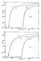
- Fig. 3 shows a graph of the drain current I d as function of the voltage to the front gate V gf , in which the SOI-NMOS-structure was held at 77 K.
- Curves A and C represent the situation in which a voltage of 3.5 Volt was supplied to the P ⁇ region 5, while in the situation of curves B and D a voltage of V D is 0.5 Volt was applied.
- the back gate 2 was pulsed starting from a DC-voltage of -20 Volt to 0, - 40 Volt resp. and vice versa, in which the difference between curves A and B on the one hand and curves C and D on the other hand was obtained.
- Curves A and B provide a threshold voltage V T of 1.2 Volt
- curves C and D provide a threshold voltage V T of 3 Volt.
- the graph of fig. 5 was obtained by cooling the structure to 4 K. Further, the circumstances for the curves E and F are similar to those for curves A and B and those of curves G and H to those for curves C and D, viz. pulses from -20 Volt to -40 Volt from -20 Volt to 0 Volt, resp.
- the pulses bias the junctions between N+- and P ⁇ region forwardly temporarily, whereby the amount of charge stored in the P ⁇ region (cavity) is influenced.
- the semiconductor element 1 according to the present invention is compact and may be driven at high rate.
- Fig. 6 shows a circuit diagram in which two transistors T1 and T2 are added to the semiconductor 1, which circuit is suited for RAM-like applications.
- terminals A, B and C By including terminals A, B and C in a matrix read/write/refresh-signals will be obtained.
- the desired voltages at terminals A, B and C are dependant on the W/L ratio of the semiconductor structure, as well as those of transistors T1 and T2.
- a typical embodiment of a SOI-NMOS-transistor com simplyprises e.g. an Si-layer 4 of 500 nm, a back oxide of e.g. 500 nm and a borium concentration of 1016 cm ⁇ 3.
- the threshold voltage V T can be influenced in this embodiments through the cavity charge Q cav , as well as through the front gate voltage V gb , which influence can be correlated. Bias voltages and pulse width(s) are dependant on the chosen thickness of the layers.
- a transistor according to the present invention is hardened to radiation influence.
- Each semiconductor element can be controlled (refreshed) through a separate back gate in future three dimensional integrated circuits.
Abstract
Description
- The present invention relates to the field of MOS-structures, more particular to a SOI-nMOS (Silicon-on-Insulator-n type-Metal-Oxide-Semiconductor) structure.
- In the international search relating to the Dutch patent of this application the following prior art references were cited:
- EP-A-0207619 (FUJITSU);
- IEEE Electron Device Letters, vol. EDL-4, No. 8, August 1983 (New York, U.S.A.), pages 269-271, B.Y. Tsaur et al.;
- IEEE Electron Device Letters, vol. EDL-4, No. 6, June 1983 (New York, U.S.A.), pages 269-271 M. Rodder et al.;
- EP-A-0114061 (HITACHI);
- IEEE Transactions on Electron Devices, vol. ED-32, No. 2, February 1985 (New York, U.S.A) pages 193-195, S.D.S. Mahli et al. - Between the first filing date (October 3, 1988) of the Dutch patent application and the present filing date, the following publications of which the content is to be seen as inserted here and which are annexed, were disclosed by one or more of the present inventors:
- The Multistable Charge Controlled Memory effect in SOI-transistors at Low Temperature, by M. Tack et al.
- "Solid State Devices", Elsevier Science Publishers B.V. (North-Holland), page 549, 1988, by D. Wouters et al.
- Proc. 1988, page 78, IEEE SOS/SOI Technology Workshop, 1988. - The present invention provides a method of operating a SOI-structure provided with a back gate, comprising the following steps:
- cooling the SOI-structure; and
- supplying and/or draining electrical charge in a cavity of the SOI-structure at predetermined times. - By the above method of claim 1 it becomes possible to influence the conducting characteristics of the MOS-structure by means of a voltage, in most cases a voltage pulse, to be supplied to the back gate. A multistable behaviour of the semiconductor structure is herewith created.
- More particularly a bistable condition of such a transistor can be obtained. This bistable condition or behaviour can be advantageously used as an elegantly simple memory element.
- Further the present invention provides a semiconductor structure.
- Further advantages, characteristics and details will become clear upon reading the following description referring to the annexed drawings.
-
- fig. 1 shows a perspective view of an embodiment of the present invention;
- fig. 2 shows a vertical section of the embodiment of fig. 1;
- fig. 3 shows a graph of measurements to the structure of fig. 1;
- fig. 4 shows a graph of measurements to the structure of fig. 1 at another temperature;
- fig. 5 shows a circuit diagram of the structure of fig. 1;
- fig. 6 shows another circuit diagram employing the semiconductor structure according to the embodiment of fig. 1;
- fig. 7 shows another circuit diagram employing the semiconductor structure according to the embodiment of fig. 1;
- fig. 8 shows another circuit diagram employing the semiconductor structure according to the embodiment of fig. 1; and
- fig. 9 shows a perspective, partly schematic view of the embodiment of fig. 1 used as radiation detector.
- A SOI-structure 1 (fig. 1 and 2) comprises a backgate 2, an insulating layer 3 and a N⁺ silicon film 4 provided thereto in which a so-called SOI cavity is included, in which a P⁻
region 5 is provided. A front insulating layer 6 is provided to the Si-layer 4 and the P⁻region 5, to which layer 6 the front gate 7 is provided. Preferably the backgate 2 comprises silicon, the layer 3 is formed of SiO₂ by means of oxydation and the film 4 is formed by deposition, after which the film is crystallized preferably by a laser. - The value of the current through the
cavity region 5, when a voltage is applied laterally thereto, will be dependent on voltages to front and back gate 7, 2 resp. - It is also possible to influence the charge QCAV in this
region 5 in a different way, e.g. by means of laser radiation, impact ionization or tunneling, in this region or in surrounding regions. - According to the present invention such a cavity charge condition is maintained during a certain time period, as such structure is being cooled. Therefore a multistable or bistable condition of the semiconductor structure is obtained, by means of which e.g. a memory effect is to be obtained. The threshold voltage VT of the P-
region 5 is adjustable such that the current characteristic of this region is controlable. - Fig. 3 shows a graph of the drain current Id as function of the voltage to the front gate Vgf, in which the SOI-NMOS-structure was held at 77 K. Curves A and C represent the situation in which a voltage of 3.5 Volt was supplied to the P⁻
region 5, while in the situation of curves B and D a voltage of VD is 0.5 Volt was applied. The back gate 2 was pulsed starting from a DC-voltage of -20 Volt to 0, - 40 Volt resp. and vice versa, in which the difference between curves A and B on the one hand and curves C and D on the other hand was obtained. Curves A and B provide a threshold voltage VT of 1.2 Volt, while curves C and D provide a threshold voltage VT of 3 Volt. - The graph of fig. 5 was obtained by cooling the structure to 4 K. Further, the circumstances for the curves E and F are similar to those for curves A and B and those of curves G and H to those for curves C and D, viz. pulses from -20 Volt to -40 Volt from -20 Volt to 0 Volt, resp.
- The pulses bias the junctions between N⁺- and P⁻ region forwardly temporarily, whereby the amount of charge stored in the P⁻ region (cavity) is influenced.
- At 77 K the structure still showed thermal degradation effects, meaning that the cavity charge QCAV was decreased considerably after some time period, while at 4 K such a condition was maintained during more than one hour. When a short pulse Vgb of e.g. -20 Volt to 0 Volt to -20 Volt is applied in the circuit diagram of fig. 5, if the element 1 is already in a condition in which VT has a high value, this structure will be confirmed in this condition. For certain values of Vgf and suitable Vd it is also possible to obtain a condition in which the structure is confirmed in this condition, if the semiconductor element shows a low VT value, e.g. Vgf=2 Volt and Vd=5 Volt.
- In this way the refreshing of such a memory cell 1 is executed, e.g. for ROM-like or EPROM-like application. The semiconductor element 1 according to the present invention is compact and may be driven at high rate.
- Fig. 6 shows a circuit diagram in which two transistors T₁ and T₂ are added to the semiconductor 1, which circuit is suited for RAM-like applications. By including terminals A, B and C in a matrix read/write/refresh-signals will be obtained. The desired voltages at terminals A, B and C are dependant on the W/L ratio of the semiconductor structure, as well as those of transistors T₁ and T₂.
- A typical embodiment of a SOI-NMOS-transistor comprises e.g. an Si-layer 4 of 500 nm, a back oxide of e.g. 500 nm and a borium concentration of 10¹⁶ cm⁻³. The threshold voltage VT can be influenced in this embodiments through the cavity charge Qcav, as well as through the front gate voltage Vgb, which influence can be correlated. Bias voltages and pulse width(s) are dependant on the chosen thickness of the layers.
- A transistor according to the present invention is hardened to radiation influence.
- Each semiconductor element can be controlled (refreshed) through a separate back gate in future three dimensional integrated circuits.
- First applications of the present invention will probably in aerospace, in high rate computers and apparatus using superconduction, in which cooling medium is available.
Claims (7)
- cooling the SOI-structure; and
- supplying and/or draining electrical charge in a cavity of the SOI-structure at predetermined times.
- a conducting back gate;
- a back oxide provided thereon;
- a silicon film provided thereon of one conducting type, provided with a recess in which a semiconducting material of the other conducting type is provided;
- a front oxide provided to said region of the other conducting type; and
- a conducting front gate provided to said front oxide.
Priority Applications (1)
| Application Number | Priority Date | Filing Date | Title |
|---|---|---|---|
| AT89202497T ATE101753T1 (en) | 1988-10-03 | 1989-10-03 | METHOD OF OPERATING A MOS STRUCTURE AND MOS STRUCTURE THEREOF. |
Applications Claiming Priority (2)
| Application Number | Priority Date | Filing Date | Title |
|---|---|---|---|
| NL8802423 | 1988-10-03 | ||
| NL8802423A NL8802423A (en) | 1988-10-03 | 1988-10-03 | METHOD FOR OPERATING A MOSS STRUCTURE AND MOSS STRUCTURE SUITABLE FOR IT. |
Publications (2)
| Publication Number | Publication Date |
|---|---|
| EP0362961A1 true EP0362961A1 (en) | 1990-04-11 |
| EP0362961B1 EP0362961B1 (en) | 1994-02-16 |
Family
ID=19852988
Family Applications (1)
| Application Number | Title | Priority Date | Filing Date |
|---|---|---|---|
| EP89202497A Expired - Lifetime EP0362961B1 (en) | 1988-10-03 | 1989-10-03 | A method of operating a MOS-structure and MOS-structure therefor |
Country Status (7)
| Country | Link |
|---|---|
| EP (1) | EP0362961B1 (en) |
| JP (1) | JPH02150066A (en) |
| AT (1) | ATE101753T1 (en) |
| CA (1) | CA1323942C (en) |
| DE (1) | DE68913119T2 (en) |
| ES (1) | ES2049317T3 (en) |
| NL (1) | NL8802423A (en) |
Cited By (21)
| Publication number | Priority date | Publication date | Assignee | Title |
|---|---|---|---|---|
| US7732816B2 (en) | 2001-06-18 | 2010-06-08 | Innovative Silicon Isi Sa | Semiconductor device |
| WO2013026237A1 (en) * | 2011-08-22 | 2013-02-28 | 中国科学院微电子研究所 | Semiconductor device |
| US8861247B2 (en) | 2009-04-27 | 2014-10-14 | Micron Technology, Inc. | Techniques for providing a direct injection semiconductor memory device |
| US8947965B2 (en) | 2009-07-27 | 2015-02-03 | Micron Technology Inc. | Techniques for providing a direct injection semiconductor memory device |
| US8964479B2 (en) | 2010-03-04 | 2015-02-24 | Micron Technology, Inc. | Techniques for sensing a semiconductor memory device |
| US8982633B2 (en) | 2009-05-22 | 2015-03-17 | Micron Technology, Inc. | Techniques for providing a direct injection semiconductor memory device |
| US9012963B2 (en) | 2011-08-22 | 2015-04-21 | Institute of Microelectronics, Chinese Academy of Sciences | Semiconductor device |
| US9019788B2 (en) | 2008-01-24 | 2015-04-28 | Micron Technology, Inc. | Techniques for accessing memory cells |
| US9019759B2 (en) | 2010-03-15 | 2015-04-28 | Micron Technology, Inc. | Techniques for providing a semiconductor memory device |
| US9064730B2 (en) | 2009-03-04 | 2015-06-23 | Micron Technology, Inc. | Techniques for forming a contact to a buried diffusion layer in a semiconductor memory device |
| US9093311B2 (en) | 2009-03-31 | 2015-07-28 | Micron Technology, Inc. | Techniques for providing a semiconductor memory device |
| US9142264B2 (en) | 2010-05-06 | 2015-09-22 | Micron Technology, Inc. | Techniques for refreshing a semiconductor memory device |
| US9240496B2 (en) | 2009-04-30 | 2016-01-19 | Micron Technology, Inc. | Semiconductor device with floating gate and electrically floating body |
| US9257155B2 (en) | 2007-05-30 | 2016-02-09 | Micron Technology, Inc. | Integrated circuit having voltage generation circuitry for memory cell array, and method of operating and/or controlling same |
| US9263133B2 (en) | 2011-05-17 | 2016-02-16 | Micron Technology, Inc. | Techniques for providing a semiconductor memory device |
| US9276000B2 (en) | 2007-03-29 | 2016-03-01 | Micron Technology, Inc. | Manufacturing process for zero-capacitor random access memory circuits |
| US9331083B2 (en) | 2009-07-10 | 2016-05-03 | Micron Technology, Inc. | Techniques for providing a semiconductor memory device |
| US9553186B2 (en) | 2008-09-25 | 2017-01-24 | Micron Technology, Inc. | Recessed gate silicon-on-insulator floating body device with self-aligned lateral isolation |
| US9812179B2 (en) | 2009-11-24 | 2017-11-07 | Ovonyx Memory Technology, Llc | Techniques for reducing disturbance in a semiconductor memory device |
| US10304837B2 (en) | 2007-11-29 | 2019-05-28 | Ovonyx Memory Technology, Llc | Integrated circuit having memory cell array including barriers, and method of manufacturing same |
| US10418091B2 (en) | 2005-09-07 | 2019-09-17 | Ovonyx Memory Technology, Llc | Memory cell and memory cell array having an electrically floating body transistor, and methods of operating same |
Families Citing this family (25)
| Publication number | Priority date | Publication date | Assignee | Title |
|---|---|---|---|---|
| US20040228168A1 (en) | 2003-05-13 | 2004-11-18 | Richard Ferrant | Semiconductor memory device and method of operating same |
| US7335934B2 (en) | 2003-07-22 | 2008-02-26 | Innovative Silicon S.A. | Integrated circuit device, and method of fabricating same |
| US7683430B2 (en) | 2005-12-19 | 2010-03-23 | Innovative Silicon Isi Sa | Electrically floating body memory cell and array, and method of operating or controlling same |
| US7492632B2 (en) | 2006-04-07 | 2009-02-17 | Innovative Silicon Isi Sa | Memory array having a programmable word length, and method of operating same |
| WO2007128738A1 (en) | 2006-05-02 | 2007-11-15 | Innovative Silicon Sa | Semiconductor memory cell and array using punch-through to program and read same |
| US8069377B2 (en) | 2006-06-26 | 2011-11-29 | Micron Technology, Inc. | Integrated circuit having memory array including ECC and column redundancy and method of operating the same |
| US7542340B2 (en) | 2006-07-11 | 2009-06-02 | Innovative Silicon Isi Sa | Integrated circuit including memory array having a segmented bit line architecture and method of controlling and/or operating same |
| WO2008090475A2 (en) | 2007-01-26 | 2008-07-31 | Innovative Silicon S.A. | Floating-body dram transistor comprising source/drain regions separated from the gated body region |
| US8085594B2 (en) | 2007-06-01 | 2011-12-27 | Micron Technology, Inc. | Reading technique for memory cell with electrically floating body transistor |
| WO2009039169A1 (en) | 2007-09-17 | 2009-03-26 | Innovative Silicon S.A. | Refreshing data of memory cells with electrically floating body transistors |
| US8349662B2 (en) | 2007-12-11 | 2013-01-08 | Micron Technology, Inc. | Integrated circuit having memory cell array, and method of manufacturing same |
| US8014195B2 (en) | 2008-02-06 | 2011-09-06 | Micron Technology, Inc. | Single transistor memory cell |
| US8189376B2 (en) | 2008-02-08 | 2012-05-29 | Micron Technology, Inc. | Integrated circuit having memory cells including gate material having high work function, and method of manufacturing same |
| US7957206B2 (en) | 2008-04-04 | 2011-06-07 | Micron Technology, Inc. | Read circuitry for an integrated circuit having memory cells and/or a memory cell array, and method of operating same |
| US7933140B2 (en) | 2008-10-02 | 2011-04-26 | Micron Technology, Inc. | Techniques for reducing a voltage swing |
| US7924630B2 (en) | 2008-10-15 | 2011-04-12 | Micron Technology, Inc. | Techniques for simultaneously driving a plurality of source lines |
| US8223574B2 (en) | 2008-11-05 | 2012-07-17 | Micron Technology, Inc. | Techniques for block refreshing a semiconductor memory device |
| US8213226B2 (en) | 2008-12-05 | 2012-07-03 | Micron Technology, Inc. | Vertical transistor memory cell and array |
| US8319294B2 (en) | 2009-02-18 | 2012-11-27 | Micron Technology, Inc. | Techniques for providing a source line plane |
| US8199595B2 (en) | 2009-09-04 | 2012-06-12 | Micron Technology, Inc. | Techniques for sensing a semiconductor memory device |
| US8310893B2 (en) | 2009-12-16 | 2012-11-13 | Micron Technology, Inc. | Techniques for reducing impact of array disturbs in a semiconductor memory device |
| US8416636B2 (en) | 2010-02-12 | 2013-04-09 | Micron Technology, Inc. | Techniques for controlling a semiconductor memory device |
| US8411513B2 (en) | 2010-03-04 | 2013-04-02 | Micron Technology, Inc. | Techniques for providing a semiconductor memory device having hierarchical bit lines |
| US8369177B2 (en) | 2010-03-05 | 2013-02-05 | Micron Technology, Inc. | Techniques for reading from and/or writing to a semiconductor memory device |
| US9559216B2 (en) | 2011-06-06 | 2017-01-31 | Micron Technology, Inc. | Semiconductor memory device and method for biasing same |
Citations (2)
| Publication number | Priority date | Publication date | Assignee | Title |
|---|---|---|---|---|
| EP0114061A2 (en) * | 1983-01-12 | 1984-07-25 | Hitachi, Ltd. | Semiconductor device having CMOS structures |
| EP0207619A1 (en) * | 1985-05-24 | 1987-01-07 | Fujitsu Limited | Semiconductor memory device |
-
1988
- 1988-10-03 NL NL8802423A patent/NL8802423A/en not_active Application Discontinuation
-
1989
- 1989-09-29 CA CA000615003A patent/CA1323942C/en not_active Expired - Fee Related
- 1989-10-03 ES ES89202497T patent/ES2049317T3/en not_active Expired - Lifetime
- 1989-10-03 EP EP89202497A patent/EP0362961B1/en not_active Expired - Lifetime
- 1989-10-03 AT AT89202497T patent/ATE101753T1/en not_active IP Right Cessation
- 1989-10-03 DE DE68913119T patent/DE68913119T2/en not_active Expired - Fee Related
- 1989-10-03 JP JP1258654A patent/JPH02150066A/en active Pending
Patent Citations (2)
| Publication number | Priority date | Publication date | Assignee | Title |
|---|---|---|---|---|
| EP0114061A2 (en) * | 1983-01-12 | 1984-07-25 | Hitachi, Ltd. | Semiconductor device having CMOS structures |
| EP0207619A1 (en) * | 1985-05-24 | 1987-01-07 | Fujitsu Limited | Semiconductor memory device |
Non-Patent Citations (3)
| Title |
|---|
| IEEE ELECTRON DEVICE LETTERS, vol. EDL-4, no. 6, June 1983, pages 193-195, IEEE; M. RODDER et al.: "Silicon-on-insulator bipolar transistors" * |
| IEEE ELECTRON DEVICE LETTERS, vol. EDL-4, no. 8, August 1983, pages 269-271, IEEE; B.-Y. TSAUR et al.: "Fully isolated lateral bipolar-MOS transistors fabricated in zone-melting-recrystallized Si films on SiO2" * |
| IEEE TRANSACTIONS ON ELECTRON DEVICES, vol. ED-32, no. 2, February 1985, pages 258-281, IEEE; S.D.S. MALHI et al.: "Characteristics and three-dimensional integration of MOSFET's in small-grain LPCVD polycrystalline silicon" * |
Cited By (27)
| Publication number | Priority date | Publication date | Assignee | Title |
|---|---|---|---|---|
| US7732816B2 (en) | 2001-06-18 | 2010-06-08 | Innovative Silicon Isi Sa | Semiconductor device |
| US11031069B2 (en) | 2005-09-07 | 2021-06-08 | Ovonyx Memory Technology, Llc | Memory cell and memory cell array having an electrically floating body transistor, and methods of operating same |
| US10418091B2 (en) | 2005-09-07 | 2019-09-17 | Ovonyx Memory Technology, Llc | Memory cell and memory cell array having an electrically floating body transistor, and methods of operating same |
| US9276000B2 (en) | 2007-03-29 | 2016-03-01 | Micron Technology, Inc. | Manufacturing process for zero-capacitor random access memory circuits |
| US9257155B2 (en) | 2007-05-30 | 2016-02-09 | Micron Technology, Inc. | Integrated circuit having voltage generation circuitry for memory cell array, and method of operating and/or controlling same |
| US10304837B2 (en) | 2007-11-29 | 2019-05-28 | Ovonyx Memory Technology, Llc | Integrated circuit having memory cell array including barriers, and method of manufacturing same |
| US11081486B2 (en) | 2007-11-29 | 2021-08-03 | Ovonyx Memory Technology, Llc | Integrated circuit having memory cell array including barriers, and method of manufacturing same |
| US9019788B2 (en) | 2008-01-24 | 2015-04-28 | Micron Technology, Inc. | Techniques for accessing memory cells |
| US9553186B2 (en) | 2008-09-25 | 2017-01-24 | Micron Technology, Inc. | Recessed gate silicon-on-insulator floating body device with self-aligned lateral isolation |
| US9064730B2 (en) | 2009-03-04 | 2015-06-23 | Micron Technology, Inc. | Techniques for forming a contact to a buried diffusion layer in a semiconductor memory device |
| US9093311B2 (en) | 2009-03-31 | 2015-07-28 | Micron Technology, Inc. | Techniques for providing a semiconductor memory device |
| US8861247B2 (en) | 2009-04-27 | 2014-10-14 | Micron Technology, Inc. | Techniques for providing a direct injection semiconductor memory device |
| US9425190B2 (en) | 2009-04-27 | 2016-08-23 | Micron Technology, Inc. | Techniques for providing a direct injection semiconductor memory device |
| US9240496B2 (en) | 2009-04-30 | 2016-01-19 | Micron Technology, Inc. | Semiconductor device with floating gate and electrically floating body |
| US8982633B2 (en) | 2009-05-22 | 2015-03-17 | Micron Technology, Inc. | Techniques for providing a direct injection semiconductor memory device |
| US9331083B2 (en) | 2009-07-10 | 2016-05-03 | Micron Technology, Inc. | Techniques for providing a semiconductor memory device |
| US9679612B2 (en) | 2009-07-27 | 2017-06-13 | Micron Technology, Inc. | Techniques for providing a direct injection semiconductor memory device |
| US8964461B2 (en) | 2009-07-27 | 2015-02-24 | Micron Technology, Inc. | Techniques for providing a direct injection semiconductor memory device |
| US8947965B2 (en) | 2009-07-27 | 2015-02-03 | Micron Technology Inc. | Techniques for providing a direct injection semiconductor memory device |
| US9812179B2 (en) | 2009-11-24 | 2017-11-07 | Ovonyx Memory Technology, Llc | Techniques for reducing disturbance in a semiconductor memory device |
| US8964479B2 (en) | 2010-03-04 | 2015-02-24 | Micron Technology, Inc. | Techniques for sensing a semiconductor memory device |
| US9019759B2 (en) | 2010-03-15 | 2015-04-28 | Micron Technology, Inc. | Techniques for providing a semiconductor memory device |
| US9524971B2 (en) | 2010-03-15 | 2016-12-20 | Micron Technology, Inc. | Techniques for providing a semiconductor memory device |
| US9142264B2 (en) | 2010-05-06 | 2015-09-22 | Micron Technology, Inc. | Techniques for refreshing a semiconductor memory device |
| US9263133B2 (en) | 2011-05-17 | 2016-02-16 | Micron Technology, Inc. | Techniques for providing a semiconductor memory device |
| US9012963B2 (en) | 2011-08-22 | 2015-04-21 | Institute of Microelectronics, Chinese Academy of Sciences | Semiconductor device |
| WO2013026237A1 (en) * | 2011-08-22 | 2013-02-28 | 中国科学院微电子研究所 | Semiconductor device |
Also Published As
| Publication number | Publication date |
|---|---|
| JPH02150066A (en) | 1990-06-08 |
| ES2049317T3 (en) | 1994-04-16 |
| NL8802423A (en) | 1990-05-01 |
| ATE101753T1 (en) | 1994-03-15 |
| DE68913119D1 (en) | 1994-03-24 |
| CA1323942C (en) | 1993-11-02 |
| EP0362961B1 (en) | 1994-02-16 |
| DE68913119T2 (en) | 1994-05-26 |
Similar Documents
| Publication | Publication Date | Title |
|---|---|---|
| EP0362961A1 (en) | A method of operating a MOS-structure and MOS-structure therefor | |
| US3660827A (en) | Bistable electrical circuit with non-volatile storage capability | |
| US6249460B1 (en) | Dynamic flash memory cells with ultrathin tunnel oxides | |
| US6909138B2 (en) | P-channel dynamic flash memory cells with ultrathin tunnel oxides | |
| US6730960B2 (en) | Static NVRAM with ultra thin tunnel oxides | |
| EP0642173A1 (en) | Semiconductor element and semiconductor memory device using the same | |
| EP0727822A2 (en) | Semiconductor memory device | |
| US4471471A (en) | Non-volatile RAM device | |
| Sherony et al. | SOI MOSFET effective channel mobility | |
| US4084108A (en) | Integrated circuit device | |
| US7449713B2 (en) | Semiconductor memory device | |
| US3646527A (en) | Electronic memory circuit employing semiconductor memory elements and a method for writing to the memory element | |
| US6147386A (en) | Semiconductor device and method of producing the same | |
| US4890011A (en) | On-chip substrate bias generating circuit having substrate potential clamp and operating method therefor | |
| JPS59204275A (en) | Manufacture of thin film transistor | |
| US4626887A (en) | Static storage cell | |
| US3922710A (en) | Semiconductor memory device | |
| JPH0586864B2 (en) | ||
| EP0504006A2 (en) | Semiconductor memory device having thin film transistor and method of producing the same | |
| Stanley | The state-of-the-art in SOI technology | |
| JPS58118090A (en) | Memory device | |
| EP0339586A2 (en) | Semiconductor device having improved gate capacitance and manufacturing method therefor | |
| JPH05226635A (en) | Thin-film semiconductor device | |
| JPH0629549A (en) | Field-effect transistor | |
| JP2002100687A (en) | Semiconductor memory device |
Legal Events
| Date | Code | Title | Description |
|---|---|---|---|
| PUAI | Public reference made under article 153(3) epc to a published international application that has entered the european phase |
Free format text: ORIGINAL CODE: 0009012 |
|
| AK | Designated contracting states |
Kind code of ref document: A1 Designated state(s): AT BE CH DE ES FR GB GR IT LI LU NL SE |
|
| 17P | Request for examination filed |
Effective date: 19900419 |
|
| 17Q | First examination report despatched |
Effective date: 19920303 |
|
| ITF | It: translation for a ep patent filed |
Owner name: STUDIO INGG. FISCHETTI & WEBER |
|
| GRAA | (expected) grant |
Free format text: ORIGINAL CODE: 0009210 |
|
| AK | Designated contracting states |
Kind code of ref document: B1 Designated state(s): AT BE CH DE ES FR GB GR IT LI LU NL SE |
|
| PG25 | Lapsed in a contracting state [announced via postgrant information from national office to epo] |
Ref country code: GR Free format text: LAPSE BECAUSE OF FAILURE TO SUBMIT A TRANSLATION OF THE DESCRIPTION OR TO PAY THE FEE WITHIN THE PRESCRIBED TIME-LIMIT Effective date: 19940216 |
|
| REF | Corresponds to: |
Ref document number: 101753 Country of ref document: AT Date of ref document: 19940315 Kind code of ref document: T |
|
| REF | Corresponds to: |
Ref document number: 68913119 Country of ref document: DE Date of ref document: 19940324 |
|
| ET | Fr: translation filed | ||
| REG | Reference to a national code |
Ref country code: ES Ref legal event code: FG2A Ref document number: 2049317 Country of ref document: ES Kind code of ref document: T3 |
|
| REG | Reference to a national code |
Ref country code: GR Ref legal event code: FG4A Free format text: 3011773 |
|
| PG25 | Lapsed in a contracting state [announced via postgrant information from national office to epo] |
Ref country code: GB Effective date: 19941003 Ref country code: AT Effective date: 19941003 |
|
| PG25 | Lapsed in a contracting state [announced via postgrant information from national office to epo] |
Ref country code: SE Effective date: 19941004 Ref country code: ES Free format text: LAPSE BECAUSE OF EXPIRATION OF PROTECTION Effective date: 19941004 |
|
| PG25 | Lapsed in a contracting state [announced via postgrant information from national office to epo] |
Ref country code: LU Free format text: LAPSE BECAUSE OF NON-PAYMENT OF DUE FEES Effective date: 19941031 Ref country code: LI Effective date: 19941031 Ref country code: CH Effective date: 19941031 Ref country code: BE Effective date: 19941031 |
|
| PLBE | No opposition filed within time limit |
Free format text: ORIGINAL CODE: 0009261 |
|
| STAA | Information on the status of an ep patent application or granted ep patent |
Free format text: STATUS: NO OPPOSITION FILED WITHIN TIME LIMIT |
|
| EAL | Se: european patent in force in sweden |
Ref document number: 89202497.7 |
|
| 26N | No opposition filed | ||
| BERE | Be: lapsed |
Owner name: INTERUNIVERSITAIR MICROELEKTRONICA CENTRUM VZW Effective date: 19941031 |
|
| PG25 | Lapsed in a contracting state [announced via postgrant information from national office to epo] |
Ref country code: NL Effective date: 19950501 |
|
| GBPC | Gb: european patent ceased through non-payment of renewal fee |
Effective date: 19941003 |
|
| NLV4 | Nl: lapsed or anulled due to non-payment of the annual fee | ||
| PG25 | Lapsed in a contracting state [announced via postgrant information from national office to epo] |
Ref country code: FR Effective date: 19950630 |
|
| REG | Reference to a national code |
Ref country code: CH Ref legal event code: PL Ref country code: GR Ref legal event code: MM2A Free format text: 3011773 |
|
| PG25 | Lapsed in a contracting state [announced via postgrant information from national office to epo] |
Ref country code: DE Effective date: 19950701 |
|
| EUG | Se: european patent has lapsed |
Ref document number: 89202497.7 |
|
| REG | Reference to a national code |
Ref country code: FR Ref legal event code: ST |
|
| REG | Reference to a national code |
Ref country code: ES Ref legal event code: FD2A Effective date: 19990601 |
|
| PG25 | Lapsed in a contracting state [announced via postgrant information from national office to epo] |
Ref country code: IT Free format text: LAPSE BECAUSE OF NON-PAYMENT OF DUE FEES;WARNING: LAPSES OF ITALIAN PATENTS WITH EFFECTIVE DATE BEFORE 2007 MAY HAVE OCCURRED AT ANY TIME BEFORE 2007. THE CORRECT EFFECTIVE DATE MAY BE DIFFERENT FROM THE ONE RECORDED. Effective date: 20051003 |