EP0352683A2 - Programmable controller module identification system - Google Patents
Programmable controller module identification system Download PDFInfo
- Publication number
- EP0352683A2 EP0352683A2 EP89113542A EP89113542A EP0352683A2 EP 0352683 A2 EP0352683 A2 EP 0352683A2 EP 89113542 A EP89113542 A EP 89113542A EP 89113542 A EP89113542 A EP 89113542A EP 0352683 A2 EP0352683 A2 EP 0352683A2
- Authority
- EP
- European Patent Office
- Prior art keywords
- module
- data
- processor
- inputs
- input port
- Prior art date
- Legal status (The legal status is an assumption and is not a legal conclusion. Google has not performed a legal analysis and makes no representation as to the accuracy of the status listed.)
- Granted
Links
Images


Classifications
-
- G—PHYSICS
- G05—CONTROLLING; REGULATING
- G05B—CONTROL OR REGULATING SYSTEMS IN GENERAL; FUNCTIONAL ELEMENTS OF SUCH SYSTEMS; MONITORING OR TESTING ARRANGEMENTS FOR SUCH SYSTEMS OR ELEMENTS
- G05B19/00—Programme-control systems
- G05B19/02—Programme-control systems electric
- G05B19/04—Programme control other than numerical control, i.e. in sequence controllers or logic controllers
- G05B19/05—Programmable logic controllers, e.g. simulating logic interconnections of signals according to ladder diagrams or function charts
- G05B19/054—Input/output
-
- G—PHYSICS
- G06—COMPUTING; CALCULATING OR COUNTING
- G06F—ELECTRIC DIGITAL DATA PROCESSING
- G06F15/00—Digital computers in general; Data processing equipment in general
- G06F15/16—Combinations of two or more digital computers each having at least an arithmetic unit, a program unit and a register, e.g. for a simultaneous processing of several programs
- G06F15/177—Initialisation or configuration control
-
- G—PHYSICS
- G05—CONTROLLING; REGULATING
- G05B—CONTROL OR REGULATING SYSTEMS IN GENERAL; FUNCTIONAL ELEMENTS OF SUCH SYSTEMS; MONITORING OR TESTING ARRANGEMENTS FOR SUCH SYSTEMS OR ELEMENTS
- G05B2219/00—Program-control systems
- G05B2219/10—Plc systems
- G05B2219/11—Plc I-O input output
- G05B2219/1185—Feedback of output status to input module and compare with command
Definitions
- the present invention relates to programmable controllers having a plurality of modules for performing different functions which operate a machine in response to the execution of a control program; and more particularly to a mechanism for identifying each type of module within the programmable controller.
- Programmable controllers are typically connected to industrial equipment, such as assembly lines and machine tools, to sequentially operate the equipment in accordance with a stored control program.
- One type of such programmable controller is disclosed in U.S. Patent No. 4,293,924 and consists of a rack which contains several functional modules.
- a rack backplane provides signal buses and connectors for electrically coupling the functional modules.
- One of these modules contains a processor which sequentially executes the control program.
- the control program is stored in a memory within the processor module and is executed to examine the condition of selected sensing devices on the controlled equipment, or to energize and deenergize selected operating devices on the controlled equipment contingent upon the status of one or more of the examined sensing devices.
- I/O input/output
- a given programmable controller can have a variety of different types of I/O modules, such as a.c. inputs or outputs, d.c. inputs or outputs, analog inputs or outputs, and open or closed loop positioning modules.
- One of the benefits of this type of programmable controller is that by varying the mix of I/O module types, the programmable controller can be configured to operate a wide variety of equipment and its configuration can be changed with alterations to the equipment.
- this advantage also presents a problem in that when a module in the programmable controller is replaced with one of a different type, the control program must be edited according. Should one of the I/O modules be inadvertently replaced with a different type of module or should an intentional replacement of the I/O modules be made without corresponding program editing, the control program will be unable to properly operate the equipment with potentially devastating consequences.
- the programmable controller prior to executing the control program, be able to identify the type of each I/O module within the system and confirm that each module corresponds to the type expected to be found by the execution of the control program.
- module identification was accomplished by storing a set of identification bytes in a read only memory of the module.
- non-intelligent I/O modules do not require such memories, and adding them solely for identification purposes would not be cost effective.
- a programmable controller has a processor for executing a control program which directs the operation of a machine to perform a specific function. Also included in the programmable controller is one or more input/output modules which interface the processor to sensing and operating devices on the machine.
- Each of the I/O modules includes circuitry which enables the processor to identify the I/O module's type. This circuitry includes an input port and an output port, each of which in the preferred embodiment is a multi-bit parallel port having a terminal for each of the parallel data bits. Both the input and output ports are addressable by the processor, enabling the processor to send data to the output port and receive data from the input port.
- the input and output ports are interconnected in a predefined manner according to the specific type of I/O module, thereby enabling the processor module by writing data to the output port and reading the data back through the input port to identify the type of I/O module.
- the general object of the present invention is to provide a programmable controller which allows its processor to identify the characteristics of each I/O module contained in the programmable controller.
- Another object is to provide such identification utilizing input and output ports on the module.
- Yet another object is to provide a system for identifying the module characteristics, which utilizes a single input and a single output port in a manner which enables a large number of different types of modules to be identified.
- a further object of the present invention is to provide such an identification system which can be expanded as the number of different types of modules increases.
- a programmable controller includes two racks 12 and 13 with separate power supplies 14 and 15 respectively.
- Each of the racks 12 and 13 has a number of slots within which different functional modules 16 and 17 can be received.
- a unique address is assigned to each rack slot in order to access the module received therein.
- the two racks 12 and 13 also include a backplane 18 and 18′ respectively, having electrical connectors and conductor buses which interconnect the functional modules 16 and 17 and provide power to the modules from the power supplies 14 and 15.
- the backplanes 18 and 18′ incorporate a parallel address bus 32, a parallel data bus 33, a set of control lines 34 and a five bit parallel slot address bus 35.
- a separate connector is provided on the backplane for each slot in the rack to couple these buses and control lines to a module in the slot.
- a multiconductor cable 20 interconnects the backplanes 18 and 18′ of the two racks 12 and 13 to form a common system backplane, designated 19.
- Another multiconductor cable 20′ extends the system backplane from the second rack 13 to other racks of the programmable controller which are not illustrated. The racks are connected in a daisy chain by the cables 20 and 20′.
- the first rack 12 contains a processor module 16 which executes a user defined control program stored in the module's memory to operate a machine coupled to the programmable controller 10.
- a programming terminal 21 is connected by a cable 22 to the processor module 16 for monitoring the operation of the programmable controller and for programming the processor module 16.
- the processor module 16 is connected to the backplane buses 32, 33 and 35 and control lines 34.
- the first rack 12 also contains a number of input/output modules 17 which electrically interface the processor 16 to sensing and operating devices on the machine controlled by the programmable controller 10.
- I/O module refers to a module which interfaces to external devices on the controlled machine. Such I/O modules can have solely an input function, solely an output function, or both input and output functions. I/O modules which provide an input function couple the processor module 16 to sensing devices on the controlled machine, while the output function modules interface to operating devices on the controlled machine.
- Each of the I/O modules may be an a.c. input or output device, a d.c. input or output device, or provide an input/output interface to analog devices, such as resolvers and position indicators.
- the typical programmable controller 10 includes a mix of different types of I/O modules.
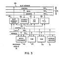
- the different components of the processor module 16, shown schematically in Figure 3, are interconnected by a set of three internal buses: a control bus 24 consisting of a number of individual control lines running between different components, a parallel data bus 25 and a parallel address bus 26.
- a microprocessor 28 is coupled to the three internal buses 24-26. Depending upon the type of microprocessor 28, the address and data signals may be multiplexed onto a shared bus with a control signal indicating which type of signal is being carried by the shared bus at any given time.
- the microprocessor 28 executes an operating system program stored in a read only memory (ROM) 29 which controls the overall operation of the programmable controller 10 and executes a user defined machine control program that is stored within a random access memory (RAM) 30.
- ROM read only memory
- RAM random access memory
- RAM 30 Also stored in RAM 30 is a standard input/output data table which retains the status of the sensing and operating devices.
- the RAM 30 also provides storage locations for counters, timers and intermediate computation values used by the microprocessor 28 in executing the operating and user control programs.
- An address decoder 31 responds to specific addresses sent over the module address bus 26 by generating control signals on bus 24 which enable the microprocessor to access memories 29 and 30, as well as the system backplane 19.
- an interbus control circuit 36 which can comprise any of several well known circuits for performing bus access arbitration.
- the interbus control circuit 36 enables a set of bidirectional data buffers 37 to couple the internal data bus 25 of the processor module 16 to the backplane data bus 33.
- the interbus control 36 enables a set of address buffers 38 to couple the processor module address bus 26 to the backplane address bus 32.
- a slot address latch 39 can be enabled by the interbus control circuit 36 to apply a five bit data word in parallel from the processor module data bus 25 to a backplane slot address bus 35.
- the interconnection of the internal buses of the processor module 16 to those of the backplane 19 enables the microprocessor 28 to selectively access any one of the I/O modules 17 in the racks 12 and 13.
- the interconnected racks are viewed as one large rack with many slots and modules.
- the slot closest to the processor module 16 is designated as slot 1 and the address of each slot going away from the processor module increases along the chain.
- the first rack 12 has seven slot addresses 0-6, including the one in which the processor module is located, and the four slots in the second rack 13 have addresses 7-10.
- the microprocessor stores the address of the module's slot in the slot address latch 39.
- the interbus control circuit 36 will then enable the slot address latch 39 to apply its contents to the slot address bus 35 across the system backplane 19.
- the backplane of each rack includes a slot address processing circuit 40, shown in Figure 2, which responds to an address of a slot within its rack by producing a slot select signal for that slot.
- the slot select signal activates the module in the respective slot to respond to signals on the other backplane buses.
- the microprocessor 28 sends the address of a component within the selected module over the backplane address bus 32 by having the interbus control circuit 36 enable the set of address buffers 38.
- the interbus control circuit 36 enables the set of data buffers 37 so that data may be exchanged between the addressed I/O module 17 and the processor module 16.
- a generic discrete input module 60 is shown schematically in Figure 4.
- the input module 60 has a component address decoder 62 coupled to the backplane address bus 32.
- the component address decoder 62 in a given module is enabled by a high level slot select signal and a high level address strobe signal from a backplane control line applied to a first AND gate 63.
- the component address decoder 62 responds to a first predefined address sent over the address bus 32 by generating a high level data input enable signal on line 64 which is connected to an input of a second AND gate 65.
- Another input of the second AND gate 65 receives an active on high I/O READ signal from a backplane control bus line 61.
- a sensor data input circuit 66 When the I/O module 60 simultaneously receives high level address strobe, slot select and I/O READ signals along with the first predefined address over the backplane buses, a sensor data input circuit 66 is enabled. This couples data from the sensing devices to the backplane data bus 33. Specifically, external sensing devices (not shown) are connected to eight data inputs of a signal level shifter circuit 67 by a set of terminals 68 on the front of the module (see Figure 1). Typically, each sensing device acts as a switch which when closed applies a given voltage level, for example 230 volts AC, to one of the data input terminals 68.
- the signal level shifter circuit 67 converts the voltage levels from the sensing devices into a relatively low voltage that is compatible with the logic devices in the programmable controller modules.
- the eight outputs of the signal level shifter 67, corresponding to the eight inputs, are connected to an isolation circuit 69 which electrically isolates the sensing devices from the remaining circuitry of the programmable controller 10.
- the isolation circuit 69 includes a separate electro-optical coupler for each data input from a sensing device.
- the eight outputs of the isolation circuit 69 are connected to the inputs of a set of eight tri-state data buffers 70 connected to the backplane data bus 33. When the data buffers 70 are enabled by a signal from the second AND gate 65, the isolation circuit outputs are coupled to lines of the backplane data bus 33. This applies the eight bits of data from the sensing devices to the processor module 16.
- the I/O module 60 also includes circuit 71 which checks the parity of each byte of data received over the data bus with a parity bit sent with the byte. If the parities do not match, the circuit 71 generates an interrupt signal on line 73 of the backplane control bus 34 which is common to all I/O modules 17.
- the interrupt signal is coupled to a periodically polled input of microprocessor 28 in the processor module 16.
- the interrupt signal also is coupled to an input of a third AND gate 72, which has another input that receives the slot select signal from the backplane slot address processing circuit 40.
- the output of the third AND gate 72 is connected to an interrupt identification (ID) control line 74 of the backplane control bus 34.
- the interrupt ID control line 74 is connected to an input of the processor modules microprocessor 28.
- the microprocessor 28 in the processor module 16 interrupts its normal program execution and commences a parity interrupt handling routine.
- This routine sequentially addresses each I/O module and inspects the level of an interrupt ID control line 74 on the backplane control bus 34 to find the interrupt generating module.
- the I/O module that generated the interrupt signal is addressed, its slot select line will go high.
- This high logic level applied to the third AND gate 72 together with the high logic level of the interrupt signal produces a high level on the interrupt ID control line 74.
- This signal on line 74 indicates to the microprocessor 28 which I/O module generated the parity interrupt and perhaps which interrupt handling routine to execute.
- an interrupt signal can be generated in response to an external signal or a module signal processing error. If several I/O modules generate separate interrupts simultaneously, each one will be polled in slot address order and their interrupts will be processed sequentially.
- each module 17 has an addressable circuit which provides several identification codes back to the processor module.
- each type of I/O module has a different set of these codes, however, the codes can also be used to distinguish among modules of the same type having different functions with respect to the controlled machine.
- the module identification circuit is illustrated in the schematic diagram of Figure 4.
- the component address decoder 62 when enabled by the slot select and address strobe signals, also responds to a second predefined address by generating a high level identification enable signal on line 76.
- This enable line 76 is coupled to inputs of fourth and fifth AND gates, 77 and 78, respectively.
- a second input of the fourth AND gate 77 is connected to an I/O write control line 79 from the backplane control bus 34.
- the output of the fourth AND gate 77 is connected to the enable input of a four bit ID output data latch 80 having its data inputs coupled to four lines of the backplane data bus 33.
- the four outputs, OB0-OB3, from the output data latch 80 are connected to two separate tri-state data buffers 81 and 82.
- Two outputs, OB1 and OB3 are coupled to the data inputs of the data buffers 81 or 82, while the other two outputs, OB0 and OB2, are connected to the output enable inputs of these data buffers.
- the outputs of the two data buffers 81 and 82 are designated ID OUT0 ⁇ and ID OUT1 respectively and form a two bit parallel output port.
- the output of the fifth AND gate 78 is coupled to the enable input of a set of five ID input data buffers 84 having their tri-state outputs connected to the five least significant bit lines of the backplane data bus 33.
- Each input IB0-IB4 of the five data buffers of set 84 is connected to an output of one of five buffer amplifiers 91-95.
- a separate pull-up resistor couples each input of the five buffer amplifiers to a source of positive voltage V+.
- the inputs of the five buffer amplifiers 91-95 are designated ID IN0 ⁇ through ID IN4 and collectively form a parallel input port.
- Identification codes for a particular I/O module are formed by connecting selected bit lines of the input port to ground potential and/or to the bit lines of the output port.
- One set of codes formed by coupling different ID input port lines ID IN0 ⁇ through ID IN4 to ground, identifies the number of inputs and outputs for the I/O module, referred to herein as I/O mix information.
- An exemplary set of these codes is given in the table of Appendix A. Thirty-two I/O mix types can be identified by these different connections of the ID input port lines. For each I/O mix type, the logic level of the five ID input port lines is shown. A "zero" in the table indicates that the line is connected to ground. A “one” in the table designates that the line is not connected to ground, but is held at a high level due to the pull-up resistor.
- a second set of identification codes provides the electrical characteristics of the module.
- An exemplary set of these codes is given in the table of Appendix B.
- the codes identifying the module's electrical characteristics are defined by connecting one or both of the ID output port lines (ID OUT0 ⁇ and ID OUT1) to a specific ID input port line. This interconnection as shown in Appendix B provides information about an input module's signal (AC, DC, etc) and the switching device of an output module (relay, triac, etc.).
- lines ID IN2, ID IN3 and ID IN4 of the input port are directly connected to ground. This grounding produces an I/O mix input bit pattern of 00011 which designates that the module has eight inputs and no outputs (see Appendix A).
- the two lines ID OUT0 ⁇ and ID OUT1 of the output port are coupled by resistors 86 and 87 to bit lines ID IN1 and ID IN0 ⁇ , respectively of the input port.
- This interconnection identifies the module as having 230 volt AC inputs (see Appendix B).
- a single input port line can be coupled to both ground and an output port line by separate resistors.
- FIG. 5A and B A flowchart of the I/O module identification routine is shown in Figures 5A and B.
- the routine commences by the microprocessor 28 of the processor module in Figure 2 initializing the variables used in the routine at step 100. Then at step 101, the microprocessor 28 loads the slot address latch 39 with the address of the rack slot containing the module 17 to be identified. Once the processor module 16 has accessed the system backplane 19, the address is sent over the slot address bus 35. In response to the slot address signal on the backplane 19, the rack slot address processing circuit 40 in the rack containing the addressed slot sends an active slot select signal to the module 17 in that slot.
- data is sent to the ID output data latches 80 which disables the ID output port at step 102.
- This is accomplished by the microprocessor 28 sending the second predefined address, that of the ID port, over the backplane address bus 32 to the module. Both the ID input and output ports share this second address with the I/O read and write control signals determining which port becomes coupled to the backplane data bus 33.
- the interbus control circuit 36 of the processor module 16 has been instructed to send active signals over the address strobe and I/O write lines of control bus 34.
- the component address decoder 62 ( Figure 4) sends an active ID enable signal on line 76.
- This enable signal combined with the active I/O write signal at the fourth AND gate 77 enable the ID output data latches 80 to store four bits of the data from the data bus 33. These four data bus bits become bits OB0-OB3 at the output of the data latches 80. Bits OB0 and OB2 are both held low and place data buffers 81 and 82 in their tri-state, or high impedance, output mode. Therefore, logic level signals are not applied via resistors 86 to 87 between the input and output ports in this mode.
- the microprocessor 28 removes the active I/O write signal and renders the I/O read signal on control line 61 active at flowchart step 103.
- This action enables the ID input data buffers 84 causing them to couple the data bits IB0-IB4 from the five buffer amplifiers 91-95 onto the data bus 33.
- These bits represent the logic levels produced by coupling selected bit lines of the ID input port to ground (i.e. lines ID IN2, ID IN3 and ID IN4 for the I/O module 60 illustrated in Figure 4).
- the microprocessor 28 reads these bits to determine the number of discrete inputs and outputs of the I/O module 60 as given by the I/O mix table of Appendix A.
- the bit pattern 00011 is generated at the input port by the ground connection of terminals ID IN2 through ID IN4 in the exemplary module 60.
- This binary pattern designates I/O mix type 3, indicating that the modules has eight inputs and no outputs as shown in Appendix A.
- This binary designation of the I/O mix for the module is stored in the RAM 30 of the processor module 16 at step 104.
- the identification routine next identifies the module's electrical characteristics. Initially at step 105, the microprocessor 28 again addresses the ID output port and stores the bit pattern (0001) in the ID output data latch 80. This pattern causes the first buffer amplifier 81 to produce a low level output (0), while maintaining the second buffer amplifier 82 in the high impedance (HI Z) tri-state condition.
- the ID input port is then read by the microprocessor 28 obtaining data bits from the ID input data buffers 84 at step 106. These data bits are stored in a location of RAM 30 designated TEMP1 at step 107.
- the microprocessor 28 changes the ID output data latch 80 to produce a high logic level from the first buffer amplifier 81 at terminal ID OUT0 ⁇ while maintaining the second buffer amplifier 82 in the tri-state condition.
- the ID input port is read again at step 109 and the results are stored in RAM 30 in a location designated TEMP2 at step 110.
- the values of TEMP1 and TEMP2 must be exclusive OR'ed (XOR). This will mask the effects of the pull up resistors and ground connections at the inputs of the five buffer amplifiers 91-95 which provide the I/O mix code.
- the result of the exclusive OR′ing at step 111 is the binary number (00010) having a one in the bit location to which the ID OUT0 ⁇ line was coupled. This number is then stored in as a variable designated STATE0 ⁇ .
- the values of STATE0 ⁇ and STATE1 must be converted into a single number that corresponds to the class of the I/O module electrical characteristics as designated in Appendix B. This conversion is carried out in the next section of the module identification routine commencing at step 119 where a bit counter variable N is set equal to 1 and a variable called CLASS is set to zero. Then, the values of STATE0 ⁇ and STATE1 are inspected to compute the electrical characteristic class. At step 120, the microprocessor 28 tests whether bit 0 ⁇ of STATE0 ⁇ equals one, which indicates that the least significant bit of the ID input port was coupled to the ID OUT0 ⁇ bit line of the ID output port. If the equality is found, the value of N is added to the variable CLASS.
- the value of STATE1 is similarly examined at step 121 and if its bit 0 ⁇ is found to equal one, six times the value of N is added to CLASS.
- the microprocessor 28 shifts the bits of variables STATE0 ⁇ and STATE1 one bit to the right so that the next least significant bit can be examined on the next loop through this section of the module identification routine.
- the bit counter N is incremented and the new value of N is tested at decision step 124 to determine if all the bits of variables STATE0 ⁇ and STATE1 have been inspected. If N is less than six, indicating bits still remain to be inspected, the routine returns to step 120. After all of the bits of variables STATE0 ⁇ and STATE1 have been examined, the routine advances to step 125.
- the value of the variable CLASS will correspond to the class of the module's electrical characteristics given in the table of Appendix B.
- the I/O mix code and the electrical characteristic code are compared at step 125 with the values defined for this module by the user during system configuration. If the codes read from the module do not match the configuration data as determined at step 126, the program execution advances to step 127 where an error message is sent to the user via terminal 21 ( Figure 1). The program execution then ends and returns to the main system program to await corrective action.
- step 126 the module identification routine tests whether additional rack slots remain at step 128. If so, the program execution returns to step 100 where the module in the next slot is identified. This process repeats for each slot and then returns to the main program.
Landscapes
- Engineering & Computer Science (AREA)
- Physics & Mathematics (AREA)
- General Physics & Mathematics (AREA)
- Computer Hardware Design (AREA)
- Theoretical Computer Science (AREA)
- Automation & Control Theory (AREA)
- Software Systems (AREA)
- General Engineering & Computer Science (AREA)
- Programmable Controllers (AREA)
Abstract
Description
- The present invention relates to programmable controllers having a plurality of modules for performing different functions which operate a machine in response to the execution of a control program; and more particularly to a mechanism for identifying each type of module within the programmable controller.
- Programmable controllers are typically connected to industrial equipment, such as assembly lines and machine tools, to sequentially operate the equipment in accordance with a stored control program. One type of such programmable controller is disclosed in U.S. Patent No. 4,293,924 and consists of a rack which contains several functional modules. A rack backplane provides signal buses and connectors for electrically coupling the functional modules. One of these modules contains a processor which sequentially executes the control program. The control program is stored in a memory within the processor module and is executed to examine the condition of selected sensing devices on the controlled equipment, or to energize and deenergize selected operating devices on the controlled equipment contingent upon the status of one or more of the examined sensing devices. Also contained within the rack are a number of input/output (I/O) modules, which interface the processor to the sensing and operating devices. A given programmable controller can have a variety of different types of I/O modules, such as a.c. inputs or outputs, d.c. inputs or outputs, analog inputs or outputs, and open or closed loop positioning modules.
- One of the benefits of this type of programmable controller is that by varying the mix of I/O module types, the programmable controller can be configured to operate a wide variety of equipment and its configuration can be changed with alterations to the equipment. However, this advantage also presents a problem in that when a module in the programmable controller is replaced with one of a different type, the control program must be edited according. Should one of the I/O modules be inadvertently replaced with a different type of module or should an intentional replacement of the I/O modules be made without corresponding program editing, the control program will be unable to properly operate the equipment with potentially devastating consequences.
- Therefore, it is desirable that the programmable controller, prior to executing the control program, be able to identify the type of each I/O module within the system and confirm that each module corresponds to the type expected to be found by the execution of the control program. Previously, module identification was accomplished by storing a set of identification bytes in a read only memory of the module. However, "non-intelligent" I/O modules do not require such memories, and adding them solely for identification purposes would not be cost effective.
- A programmable controller has a processor for executing a control program which directs the operation of a machine to perform a specific function. Also included in the programmable controller is one or more input/output modules which interface the processor to sensing and operating devices on the machine. Each of the I/O modules includes circuitry which enables the processor to identify the I/O module's type. This circuitry includes an input port and an output port, each of which in the preferred embodiment is a multi-bit parallel port having a terminal for each of the parallel data bits. Both the input and output ports are addressable by the processor, enabling the processor to send data to the output port and receive data from the input port. The input and output ports are interconnected in a predefined manner according to the specific type of I/O module, thereby enabling the processor module by writing data to the output port and reading the data back through the input port to identify the type of I/O module.
- The general object of the present invention is to provide a programmable controller which allows its processor to identify the characteristics of each I/O module contained in the programmable controller.
- Another object is to provide such identification utilizing input and output ports on the module.
- Yet another object is to provide a system for identifying the module characteristics, which utilizes a single input and a single output port in a manner which enables a large number of different types of modules to be identified.
- A further object of the present invention is to provide such an identification system which can be expanded as the number of different types of modules increases.
-
- FIGURE 1 is a pictorial representation of a programmable controller according to the present invention;
- FIGURE 2 is a schematic representation of the electrical interconnecticn of the racks and modules of the programmable controller;
- FIGURE 3 is a schematic block diagram of the programmable controller processor module;
- FIGURE 4 is a block schematic diagram of a generic input type I/O module; and
- FIGURES 5A and 5B form a flowchart of a module identification routine, which is executed by the processor module.
- With initial reference to Figures 1 and 2, a programmable controller, generally designated as 10, includes two
racks 12 and 13 withseparate power supplies racks 12 and 13 has a number of slots within which differentfunctional modules racks 12 and 13 also include abackplane functional modules power supplies backplanes parallel address bus 32, aparallel data bus 33, a set ofcontrol lines 34 and a five bit parallelslot address bus 35. Although separate address and data buses have been shown, a common bus onto which both address and data signals are time multiplexed can also be used. A separate connector is provided on the backplane for each slot in the rack to couple these buses and control lines to a module in the slot. Amulticonductor cable 20 interconnects thebackplanes racks 12 and 13 to form a common system backplane, designated 19. Anothermulticonductor cable 20′ extends the system backplane from the second rack 13 to other racks of the programmable controller which are not illustrated. The racks are connected in a daisy chain by thecables - The
first rack 12 contains aprocessor module 16 which executes a user defined control program stored in the module's memory to operate a machine coupled to the programmable controller 10. Aprogramming terminal 21 is connected by a cable 22 to theprocessor module 16 for monitoring the operation of the programmable controller and for programming theprocessor module 16. Theprocessor module 16 is connected to thebackplane buses control lines 34. - The
first rack 12 also contains a number of input/output modules 17 which electrically interface theprocessor 16 to sensing and operating devices on the machine controlled by the programmable controller 10. As used herein, the term I/O module refers to a module which interfaces to external devices on the controlled machine. Such I/O modules can have solely an input function, solely an output function, or both input and output functions. I/O modules which provide an input function couple theprocessor module 16 to sensing devices on the controlled machine, while the output function modules interface to operating devices on the controlled machine. Each of the I/O modules may be an a.c. input or output device, a d.c. input or output device, or provide an input/output interface to analog devices, such as resolvers and position indicators. The typical programmable controller 10 includes a mix of different types of I/O modules. - The different components of the
processor module 16, shown schematically in Figure 3, are interconnected by a set of three internal buses: acontrol bus 24 consisting of a number of individual control lines running between different components, a parallel data bus 25 and a parallel address bus 26. Amicroprocessor 28 is coupled to the three internal buses 24-26. Depending upon the type ofmicroprocessor 28, the address and data signals may be multiplexed onto a shared bus with a control signal indicating which type of signal is being carried by the shared bus at any given time. Themicroprocessor 28 executes an operating system program stored in a read only memory (ROM) 29 which controls the overall operation of the programmable controller 10 and executes a user defined machine control program that is stored within a random access memory (RAM) 30. Also stored inRAM 30 is a standard input/output data table which retains the status of the sensing and operating devices. TheRAM 30 also provides storage locations for counters, timers and intermediate computation values used by themicroprocessor 28 in executing the operating and user control programs. Anaddress decoder 31 responds to specific addresses sent over the module address bus 26 by generating control signals onbus 24 which enable the microprocessor to accessmemories system backplane 19. - Access to the
system backplane 19 by either theprocessor module 16 or by another module is governed by aninterbus control circuit 36 which can comprise any of several well known circuits for performing bus access arbitration. In response to the proper request signal, theinterbus control circuit 36 enables a set ofbidirectional data buffers 37 to couple the internal data bus 25 of theprocessor module 16 to thebackplane data bus 33. Similarly, theinterbus control 36 enables a set of address buffers 38 to couple the processor module address bus 26 to thebackplane address bus 32. A slot address latch 39 can be enabled by theinterbus control circuit 36 to apply a five bit data word in parallel from the processor module data bus 25 to a backplaneslot address bus 35. - The interconnection of the internal buses of the
processor module 16 to those of thebackplane 19 enables themicroprocessor 28 to selectively access any one of the I/O modules 17 in theracks 12 and 13. As far as the operation of theprocessor module 16 is concerned, the interconnected racks are viewed as one large rack with many slots and modules. In such a system, the slot closest to theprocessor module 16 is designated asslot 1 and the address of each slot going away from the processor module increases along the chain. Thefirst rack 12 has seven slot addresses 0-6, including the one in which the processor module is located, and the four slots in the second rack 13 have addresses 7-10. To address a given module, the microprocessor stores the address of the module's slot in the slot address latch 39. Theinterbus control circuit 36 will then enable the slot address latch 39 to apply its contents to theslot address bus 35 across thesystem backplane 19. The backplane of each rack includes a slotaddress processing circuit 40, shown in Figure 2, which responds to an address of a slot within its rack by producing a slot select signal for that slot. The slot select signal activates the module in the respective slot to respond to signals on the other backplane buses. Once the slot address has been sent, themicroprocessor 28 sends the address of a component within the selected module over thebackplane address bus 32 by having theinterbus control circuit 36 enable the set of address buffers 38. At the same time theinterbus control circuit 36 enables the set of data buffers 37 so that data may be exchanged between the addressed I/O module 17 and theprocessor module 16. - By employing this addressing technique, the
processor module 16 can acquire sensor data from input modules and send state data to the operating devices via output modules in the racks. A genericdiscrete input module 60 is shown schematically in Figure 4. Theinput module 60 has acomponent address decoder 62 coupled to thebackplane address bus 32. Thecomponent address decoder 62 in a given module is enabled by a high level slot select signal and a high level address strobe signal from a backplane control line applied to a first ANDgate 63. When enabled, thecomponent address decoder 62 responds to a first predefined address sent over theaddress bus 32 by generating a high level data input enable signal online 64 which is connected to an input of a second ANDgate 65. Another input of the second ANDgate 65 receives an active on high I/O READ signal from a backplanecontrol bus line 61. - When the I/
O module 60 simultaneously receives high level address strobe, slot select and I/O READ signals along with the first predefined address over the backplane buses, a sensordata input circuit 66 is enabled. This couples data from the sensing devices to thebackplane data bus 33. Specifically, external sensing devices (not shown) are connected to eight data inputs of a signallevel shifter circuit 67 by a set ofterminals 68 on the front of the module (see Figure 1). Typically, each sensing device acts as a switch which when closed applies a given voltage level, for example 230 volts AC, to one of thedata input terminals 68. The signallevel shifter circuit 67 converts the voltage levels from the sensing devices into a relatively low voltage that is compatible with the logic devices in the programmable controller modules. The eight outputs of thesignal level shifter 67, corresponding to the eight inputs, are connected to anisolation circuit 69 which electrically isolates the sensing devices from the remaining circuitry of the programmable controller 10. Theisolation circuit 69 includes a separate electro-optical coupler for each data input from a sensing device. The eight outputs of theisolation circuit 69 are connected to the inputs of a set of eight tri-state data buffers 70 connected to thebackplane data bus 33. When the data buffers 70 are enabled by a signal from the second ANDgate 65, the isolation circuit outputs are coupled to lines of thebackplane data bus 33. This applies the eight bits of data from the sensing devices to theprocessor module 16. - The I/
O module 60 also includescircuit 71 which checks the parity of each byte of data received over the data bus with a parity bit sent with the byte. If the parities do not match, thecircuit 71 generates an interrupt signal online 73 of thebackplane control bus 34 which is common to all I/O modules 17. The interrupt signal is coupled to a periodically polled input ofmicroprocessor 28 in theprocessor module 16. The interrupt signal also is coupled to an input of a third ANDgate 72, which has another input that receives the slot select signal from the backplane slotaddress processing circuit 40. The output of the third ANDgate 72 is connected to an interrupt identification (ID)control line 74 of thebackplane control bus 34. The interruptID control line 74 is connected to an input of theprocessor modules microprocessor 28. - When a high logic level interrupt signal is generated by the
parity checking circuit 71, themicroprocessor 28 in theprocessor module 16 interrupts its normal program execution and commences a parity interrupt handling routine. This routine sequentially addresses each I/O module and inspects the level of an interruptID control line 74 on thebackplane control bus 34 to find the interrupt generating module. When the I/O module that generated the interrupt signal is addressed, its slot select line will go high. This high logic level applied to the third ANDgate 72 together with the high logic level of the interrupt signal produces a high level on the interruptID control line 74. This signal online 74 indicates to themicroprocessor 28 which I/O module generated the parity interrupt and perhaps which interrupt handling routine to execute. In other types of I/O modules, an interrupt signal can be generated in response to an external signal or a module signal processing error. If several I/O modules generate separate interrupts simultaneously, each one will be polled in slot address order and their interrupts will be processed sequentially. - As the I/
O modules 17 are interchangeable in the rack slots, a potential exists that two or more modules may be inserted in different slots than the ones designated in the control program. If the modules are incorrectly positioned in the racks, different sensing and operating devices will be addressed by the processor during program execution. In order to detect erroneously located modules, each module has an addressable circuit which provides several identification codes back to the processor module. Typically, each type of I/O module has a different set of these codes, however, the codes can also be used to distinguish among modules of the same type having different functions with respect to the controlled machine. - The module identification circuit is illustrated in the schematic diagram of Figure 4. The
component address decoder 62, when enabled by the slot select and address strobe signals, also responds to a second predefined address by generating a high level identification enable signal online 76. This enableline 76 is coupled to inputs of fourth and fifth AND gates, 77 and 78, respectively. A second input of the fourth ANDgate 77 is connected to an I/Owrite control line 79 from thebackplane control bus 34. The output of the fourth ANDgate 77 is connected to the enable input of a four bit ID output data latch 80 having its data inputs coupled to four lines of thebackplane data bus 33. The four outputs, OB₀-OB₃, from the output data latch 80 are connected to two separate tri-state data buffers 81 and 82. Two outputs, OB₁ and OB₃, are coupled to the data inputs of the data buffers 81 or 82, while the other two outputs, OB₀ and OB₂, are connected to the output enable inputs of these data buffers. The outputs of the twodata buffers 81 and 82 are designated ID OUT0̸ and ID OUT1 respectively and form a two bit parallel output port. - The output of the fifth AND gate 78 is coupled to the enable input of a set of five ID input data buffers 84 having their tri-state outputs connected to the five least significant bit lines of the
backplane data bus 33. Each input IB₀-IB₄ of the five data buffers ofset 84 is connected to an output of one of five buffer amplifiers 91-95. A separate pull-up resistor couples each input of the five buffer amplifiers to a source of positive voltage V⁺. The inputs of the five buffer amplifiers 91-95 are designated ID IN0̸ through ID IN4 and collectively form a parallel input port. - Identification codes for a particular I/O module are formed by connecting selected bit lines of the input port to ground potential and/or to the bit lines of the output port. One set of codes, formed by coupling different ID input port lines ID IN0̸ through ID IN4 to ground, identifies the number of inputs and outputs for the I/O module, referred to herein as I/O mix information. An exemplary set of these codes is given in the table of Appendix A. Thirty-two I/O mix types can be identified by these different connections of the ID input port lines. For each I/O mix type, the logic level of the five ID input port lines is shown. A "zero" in the table indicates that the line is connected to ground. A "one" in the table designates that the line is not connected to ground, but is held at a high level due to the pull-up resistor.
- A second set of identification codes provides the electrical characteristics of the module. An exemplary set of these codes is given in the table of Appendix B. The codes identifying the module's electrical characteristics are defined by connecting one or both of the ID output port lines (ID OUT0̸ and ID OUT1) to a specific ID input port line. This interconnection as shown in Appendix B provides information about an input module's signal (AC, DC, etc) and the switching device of an output module (relay, triac, etc.).
- With reference to the specific I/
O module 60 illustrated in Figure 4, lines ID IN2, ID IN3 and ID IN4 of the input port are directly connected to ground. This grounding produces an I/O mix input bit pattern of 00011 which designates that the module has eight inputs and no outputs (see Appendix A). The two lines ID OUT0̸ and ID OUT1 of the output port are coupled byresistors - Whenever the
processor module 16 is placed in the control program execution mode, it initially conducts a scan of each rack slot to determine the type of module in that slot. A flowchart of the I/O module identification routine is shown in Figures 5A and B. The routine commences by themicroprocessor 28 of the processor module in Figure 2 initializing the variables used in the routine atstep 100. Then atstep 101, themicroprocessor 28 loads the slot address latch 39 with the address of the rack slot containing themodule 17 to be identified. Once theprocessor module 16 has accessed thesystem backplane 19, the address is sent over theslot address bus 35. In response to the slot address signal on thebackplane 19, the rack slotaddress processing circuit 40 in the rack containing the addressed slot sends an active slot select signal to themodule 17 in that slot. - Then, data is sent to the ID output data latches 80 which disables the ID output port at
step 102. This is accomplished by themicroprocessor 28 sending the second predefined address, that of the ID port, over thebackplane address bus 32 to the module. Both the ID input and output ports share this second address with the I/O read and write control signals determining which port becomes coupled to thebackplane data bus 33. At this time, theinterbus control circuit 36 of theprocessor module 16 has been instructed to send active signals over the address strobe and I/O write lines ofcontrol bus 34. In response to these signals, the component address decoder 62 (Figure 4) sends an active ID enable signal online 76. This enable signal combined with the active I/O write signal at the fourth ANDgate 77 enable the ID output data latches 80 to store four bits of the data from thedata bus 33. These four data bus bits become bits OB₀-OB₃ at the output of the data latches 80. Bits OB₀ and OB₂ are both held low and place data buffers 81 and 82 in their tri-state, or high impedance, output mode. Therefore, logic level signals are not applied viaresistors 86 to 87 between the input and output ports in this mode. - With the ID port address still being sent over the
address bus 32, themicroprocessor 28 removes the active I/O write signal and renders the I/O read signal oncontrol line 61 active atflowchart step 103. This action enables the ID input data buffers 84 causing them to couple the data bits IB₀-IB₄ from the five buffer amplifiers 91-95 onto thedata bus 33. These bits represent the logic levels produced by coupling selected bit lines of the ID input port to ground (i.e. lines ID IN2, ID IN3 and ID IN4 for the I/O module 60 illustrated in Figure 4). Themicroprocessor 28 reads these bits to determine the number of discrete inputs and outputs of the I/O module 60 as given by the I/O mix table of Appendix A. As described above, the bit pattern 00011 is generated at the input port by the ground connection of terminals ID IN2 through ID IN4 in theexemplary module 60.. This binary pattern designates I/O mix type 3, indicating that the modules has eight inputs and no outputs as shown in Appendix A. This binary designation of the I/O mix for the module is stored in theRAM 30 of theprocessor module 16 atstep 104. - The identification routine next identifies the module's electrical characteristics. Initially at
step 105, themicroprocessor 28 again addresses the ID output port and stores the bit pattern (0001) in the ID output data latch 80. This pattern causes thefirst buffer amplifier 81 to produce a low level output (0), while maintaining the second buffer amplifier 82 in the high impedance (HI Z) tri-state condition. The ID input port is then read by themicroprocessor 28 obtaining data bits from the ID input data buffers 84 atstep 106. These data bits are stored in a location ofRAM 30 designated TEMP1 atstep 107. Then atstep 108, themicroprocessor 28 changes the ID output data latch 80 to produce a high logic level from thefirst buffer amplifier 81 at terminal ID OUT0̸ while maintaining the second buffer amplifier 82 in the tri-state condition. The ID input port is read again atstep 109 and the results are stored inRAM 30 in a location designated TEMP2 atstep 110. - In order to determine to which ID input port lines the ID OUT0̸ terminal is coupled, the values of TEMP1 and TEMP2 must be exclusive OR'ed (XOR). This will mask the effects of the pull up resistors and ground connections at the inputs of the five buffer amplifiers 91-95 which provide the I/O mix code. The result of the exclusive OR′ing at
step 111 is the binary number (00010) having a one in the bit location to which the ID OUT0̸ line was coupled. This number is then stored in as a variable designated STATE0̸. - The process of toggling one of the ID output port lines between one and zero and reading the ID input port is repeated at
steps 112 through 117 for output port line ID OUT1. The results read from the ID input port, TEMP3 and TEMP4 are exclusive OR'ed to produce a binary number (00001) assigned to variable STATE1, which indicates the bit line of the input port that is coupled to bit line ID OUT1 of the output port atstep 118 on Figure 6B. - The values of STATE0̸ and STATE1 must be converted into a single number that corresponds to the class of the I/O module electrical characteristics as designated in Appendix B. This conversion is carried out in the next section of the module identification routine commencing at
step 119 where a bit counter variable N is set equal to 1 and a variable called CLASS is set to zero. Then, the values of STATE0̸ and STATE1 are inspected to compute the electrical characteristic class. Atstep 120, themicroprocessor 28 tests whether bit 0̸ of STATE0̸ equals one, which indicates that the least significant bit of the ID input port was coupled to the ID OUT0̸ bit line of the ID output port. If the equality is found, the value of N is added to the variable CLASS. The value of STATE1 is similarly examined atstep 121 and if its bit 0̸ is found to equal one, six times the value of N is added to CLASS. Atstep 122, themicroprocessor 28 shifts the bits of variables STATE0̸ and STATE1 one bit to the right so that the next least significant bit can be examined on the next loop through this section of the module identification routine. Then atstep 123, the bit counter N is incremented and the new value of N is tested atdecision step 124 to determine if all the bits of variables STATE0̸ and STATE1 have been inspected. If N is less than six, indicating bits still remain to be inspected, the routine returns to step 120. After all of the bits of variables STATE0̸ and STATE1 have been examined, the routine advances to step 125. - Once all of the bits have been examined, the value of the variable CLASS will correspond to the class of the module's electrical characteristics given in the table of Appendix B. The I/O mix code and the electrical characteristic code are compared at
step 125 with the values defined for this module by the user during system configuration. If the codes read from the module do not match the configuration data as determined atstep 126, the program execution advances to step 127 where an error message is sent to the user via terminal 21 (Figure 1). The program execution then ends and returns to the main system program to await corrective action. - If at
step 126 the module is found to be as specified in the system configuration data, the module identification routine tests whether additional rack slots remain atstep 128. If so, the program execution returns to step 100 where the module in the next slot is identified. This process repeats for each slot and then returns to the main program.APPENDIX A I/O MIX INFORMATION ID INPUT PORT LINE I/ O MIX TYPE 4 3 2 1 0 NO. OF INPUTS NO. OF OUTPUTS 0 0 0 0 0 0 2 0 1 0 0 0 0 1 4 0 2 0 0 0 1 0 6 0 3 0 0 0 1 1 8 0 4 0 0 1 0 0 12 0 5 0 0 1 0 1 16 0 6 0 0 1 1 0 24 0 7 0 0 1 1 1 32 0 8 0 1 0 0 0 2 2 9 0 1 0 0 1 2 4 10 0 1 0 1 0 4 2 11 0 1 0 1 1 4 4 12 0 1 1 0 0 4 6 13 0 1 1 0 1 4 8 14 0 1 1 1 0 6 4 15 0 1 1 1 1 6 6 16 1 0 0 0 0 6 8 17 1 0 0 0 1 8 4 18 1 0 0 1 0 8 6 19 1 0 0 1 1 8 8 20 1 0 1 0 0 UNDEFINED 21 1 0 1 0 1 UNDEFINED 22 1 0 1 1 0 UNDEFINED 23 1 0 1 1 1 UNDEFINED 24 1 1 0 0 0 0 2 25 1 1 0 0 1 0 4 26 1 1 0 1 0 0 6 27 1 1 0 1 1 0 8 28 1 1 1 0 0 0 12 29 1 1 1 0 1 0 16 30 1 1 1 1 0 0 24 31 1 1 1 1 1 0 32 APPENDIX B I/O MODULE ELECTRICAL CHARACTERISTICS CLASS ID OUT1 ID OUTØ INPUT TYPE OUTPUT TYPE 0 OPEN OPEN 115 VAC RELAY 1 OPEN ID INØ 230 VAC RELAY 2 OPEN ID IN1 115/230 VAC RELAY 3 OPEN ID IN2 115 VAC TRIAC 4 OPEN ID IN3 230 VAC TRIAC 5 OPEN ID IN4 115/230 VAC TRIAC 6 ID INØ OPEN 24 VDC (SINK) TRIAC 7 ID INØ ID INØ 115 VAC TRIAC (ZERO CROSS) 8 ID INØ ID IN1 230 VAC TRIAC (ZERO CROSS) 9 ID INØ ID IN2 115/230 VAC TRIAC (ZERO CROSS) 10 ID INØ ID IN3 24 VAC/VDC TRIAC (ZERO CROSS) 11 ID INØ ID IN4 24 VAC/VDC RELAY 12 ID IN1 OPEN 24 VDC (SINK) RELAY 13 ID IN1 ID INØ 24 VDC (SINK) TRANSISTOR (SOURCE) 14 ID IN1 ID IN1 24 VDC (SINK) TRANSISTOR (SINK) 15 ID IN1 ID IN2 TTL TTL 16 ID IN1 ID IN3 BCD BCD 17 ID IN1 ID IN4 ANALOG UNDEFINED 18 ID IN2 OPEN 24 VAC/VDC TRIAC 19 ID IN2 ID INØ 24 VDC (SINK) TRAIC (ZERO CROSS) 20 ID IN2 ID IN1 24 VDC (SOURCE) RELAY 21 ID IN2 ID IN2 24 VDC (SOURCE) TRANSISTOR (SOURCE) 22 ID IN2 ID IN3 24 VDC (SOURCE) TRANSISTOR (SINK) 23 ID IN2 ID IN4 24 VDC (SOURCE) TRIAC 24 ID IN3 OPEN 24 VDC (SOURCE) TRIAC (ZERO CROSS) 25 ID IN3 ID INØ UNDEFINED UNDEFINED 26 ID IN3 ID IN1 UNDEFINED UNDEFINED 27 ID IN3 ID IN2 UNDEFINED UNDEFINED 28 ID IN3 ID IN3 UNDEFINED UNDEFINED 29 ID IN3 ID IN4 UNDEFINED UNDEFINED 30 ID IN4 OPEN UNDEFINED UNDEFINED 31 ID IN4 ID INØ UNDEFINED UNDEFINED 32 ID IN4 ID IN1 UNDEFINED UNDEFINED 33 ID IN4 ID IN2 UNDEFINED UNDEFINED 34 ID IN4 ID IN3 UNDEFINED UNDEFINED 35 ID IN4 ID IN4 UNDEFINED UNDEFINED
Claims (14)
an output port addressable by said processor;
an input port addressable by said processor;
means for coupling said input port to said output port in a manner that encodes data regarding the characteristics of the functional module.
said output port includes a plurality of parallel data bit outputs;
said input port includes a plurality of parallel data bit inputs; and
said means for coupling connects ones of the data bit outputs to selected ones of the data bit inputs whereby a pattern of connection encodes data regarding the functional module.
a parallel data output port having a plurality of outputs, and being addressable by said processor to send data from said output port;
a parallel data input port having a plurality of inputs, and being addressable by said processor to receive data from said input port; and
means for coupling selected outputs of said output port to selected inputs of said input port in a predefined manner which identifies the I/O module.
an output port addressable by said processor;
an input port addressable by said processor; and
means for coupling said input port to said output port in a manner that encodes data regarding the module.
said output port includes a plurality of parallel data outputs;
said input port includes a plurality of parallel data inputs; and
said means for coupling connects said outputs to selected inputs whereby said pattern of connection provides data regarding the I/O module.
said output port includes a plurality of parallel data outputs;
said input port includes a plurality of parallel data inputs; and
said means for coupling connects said outputs to selected inputs whereby said pattern of connection provides a first data code; and
means for coupling each of said data inputs to a positive or a negative voltage source.whereby said pattern of connection to the voltage sources provides a second data code.
Applications Claiming Priority (2)
| Application Number | Priority Date | Filing Date | Title |
|---|---|---|---|
| US22380988A | 1988-07-25 | 1988-07-25 | |
| US223809 | 1988-07-25 |
Publications (3)
| Publication Number | Publication Date |
|---|---|
| EP0352683A2 true EP0352683A2 (en) | 1990-01-31 |
| EP0352683A3 EP0352683A3 (en) | 1990-08-29 |
| EP0352683B1 EP0352683B1 (en) | 1994-12-21 |
Family
ID=22838059
Family Applications (1)
| Application Number | Title | Priority Date | Filing Date |
|---|---|---|---|
| EP19890113542 Expired - Lifetime EP0352683B1 (en) | 1988-07-25 | 1989-07-23 | Programmable controller module identification system |
Country Status (4)
| Country | Link |
|---|---|
| EP (1) | EP0352683B1 (en) |
| JP (1) | JPH0241502A (en) |
| CA (1) | CA1318406C (en) |
| DE (1) | DE68920084T2 (en) |
Cited By (15)
| Publication number | Priority date | Publication date | Assignee | Title |
|---|---|---|---|---|
| EP0490864A1 (en) * | 1990-12-11 | 1992-06-17 | Fisher Controls International, Inc. | Process controller with modular I/O units |
| EP0500118A1 (en) * | 1991-02-22 | 1992-08-26 | Allen-Bradley Company, Inc. | Multiple adapter response detection circuit |
| EP0524890A1 (en) * | 1991-07-26 | 1993-01-27 | Esswein S.A. | Household appliance with a microprocessor timer controlling a display |
| US5339425A (en) * | 1990-12-11 | 1994-08-16 | Fisher Controls International, Inc. | Operating system for a process controller |
| EP0620510A1 (en) * | 1993-04-15 | 1994-10-19 | Siemens Aktiengesellschaft | Electrical apparatus with a configurable interface |
| DE4446286C1 (en) * | 1994-12-23 | 1996-06-20 | Siemens Ag | Responsive signal processing system and method for producing a responsive system |
| WO1997050025A1 (en) * | 1996-06-21 | 1997-12-31 | Siemens Aktiengesellschaft | Process automation system |
| US5752033A (en) * | 1994-05-16 | 1998-05-12 | Mitsubishi Denki Kabushiki Kaisha | Programming device for programmable controller, functional unit for programmable controller, and method of inputting memory display for programming device |
| EP0776494B1 (en) * | 1994-08-19 | 1998-08-26 | Siemens Aktiengesellschaft | Arrangement with a signal processing connection and a functional unit |
| DE19914206A1 (en) * | 1999-03-29 | 2000-07-13 | Siemens Ag | Method of automatically ascertaining process display addresses of individual channels of interconnected devices, such as sensors and actuators exchanging signals with supervisory automated equipment |
| DE10047060A1 (en) * | 2000-09-22 | 2002-05-08 | Schneider Automation Gmbh | Production system is formed from configuration of modules with code for compatibility |
| WO2003065137A1 (en) * | 2002-02-01 | 2003-08-07 | Dr. Johannes Heidenhain Gmbh | Method for examining an interface |
| US6812596B2 (en) * | 2000-04-22 | 2004-11-02 | Pilz Gmbh & Co. | Safety switching device module arrangement |
| DE102004049771A1 (en) * | 2004-10-12 | 2006-04-13 | Endress + Hauser Flowtec Ag | Method for operating a modular field device of automation technology |
| DE102005027047A1 (en) * | 2005-06-10 | 2006-12-14 | Endress + Hauser Wetzer Gmbh + Co. Kg | Measuring transducer feeder for use in process automation technology, has signaling device signaling additional information, which is supplied by measuring transducer, and transmitting information to microcontroller via signal line |
Families Citing this family (2)
| Publication number | Priority date | Publication date | Assignee | Title |
|---|---|---|---|---|
| SE524929C2 (en) * | 2002-06-07 | 2004-10-26 | Abb Ab | A control system with physically separated modules for controlling one or more manipulators |
| DE102004040449B4 (en) * | 2004-08-20 | 2009-02-26 | Siemens Ag | Automation device with one CPU and one master unit |
Citations (3)
| Publication number | Priority date | Publication date | Assignee | Title |
|---|---|---|---|---|
| DE3125011A1 (en) * | 1980-06-25 | 1982-04-01 | Gorenje TGO n.sol.o., Velenje, 63320 Velenje | Circuit arrangement for modifying input/output addresses for a programmable logic control unit |
| US4468612A (en) * | 1982-01-15 | 1984-08-28 | At&T Bell Laboratories | Arrangement for indicating when different types of electrical components are interconnected |
| US4470113A (en) * | 1981-01-13 | 1984-09-04 | Nippon Electric Co., Ltd. | Information processing unit |
Family Cites Families (4)
| Publication number | Priority date | Publication date | Assignee | Title |
|---|---|---|---|---|
| JPS55118120A (en) * | 1979-03-02 | 1980-09-10 | Fuji Electric Co Ltd | Setting system for type-based information of input/output card |
| JPS6149261A (en) * | 1984-08-17 | 1986-03-11 | Fujitsu Ltd | Additional unit identifying method |
| US4691296A (en) * | 1984-11-16 | 1987-09-01 | Allen-Bradley Company, Inc. | Method and apparatus for exchanging multiple data bytes with an I/O module in a single scan. |
| JPS61226866A (en) * | 1985-03-30 | 1986-10-08 | Usac Electronics Ind Co Ltd | Automatic discriminating system for substrate |
-
1989
- 1989-03-21 CA CA000594338A patent/CA1318406C/en not_active Expired - Lifetime
- 1989-05-16 JP JP12271689A patent/JPH0241502A/en active Pending
- 1989-07-23 DE DE1989620084 patent/DE68920084T2/en not_active Expired - Lifetime
- 1989-07-23 EP EP19890113542 patent/EP0352683B1/en not_active Expired - Lifetime
Patent Citations (3)
| Publication number | Priority date | Publication date | Assignee | Title |
|---|---|---|---|---|
| DE3125011A1 (en) * | 1980-06-25 | 1982-04-01 | Gorenje TGO n.sol.o., Velenje, 63320 Velenje | Circuit arrangement for modifying input/output addresses for a programmable logic control unit |
| US4470113A (en) * | 1981-01-13 | 1984-09-04 | Nippon Electric Co., Ltd. | Information processing unit |
| US4468612A (en) * | 1982-01-15 | 1984-08-28 | At&T Bell Laboratories | Arrangement for indicating when different types of electrical components are interconnected |
Non-Patent Citations (1)
| Title |
|---|
| COMPUTER TECHNOLOGY REVIEW. vol. VII, no. 13, 1987, LOS ANGELES US pages 24 - 29; R. FINGER: "The interconnect Space of MULTIBUS II Simplifies Hardware/Software Use" * |
Cited By (23)
| Publication number | Priority date | Publication date | Assignee | Title |
|---|---|---|---|---|
| EP0490864A1 (en) * | 1990-12-11 | 1992-06-17 | Fisher Controls International, Inc. | Process controller with modular I/O units |
| US5339425A (en) * | 1990-12-11 | 1994-08-16 | Fisher Controls International, Inc. | Operating system for a process controller |
| AU658842B2 (en) * | 1990-12-11 | 1995-05-04 | Fisher Controls International Inc. | Process controller with modular input/output units |
| US5901323A (en) * | 1990-12-11 | 1999-05-04 | Fisher Controls International, Inc. | Process controller with interchangeable individual I/O units |
| EP0500118A1 (en) * | 1991-02-22 | 1992-08-26 | Allen-Bradley Company, Inc. | Multiple adapter response detection circuit |
| EP0524890A1 (en) * | 1991-07-26 | 1993-01-27 | Esswein S.A. | Household appliance with a microprocessor timer controlling a display |
| FR2679668A1 (en) * | 1991-07-26 | 1993-01-29 | Esswein Sa | MICROPROCESSOR PROGRAMMER ELECTRICAL APPLIANCE CONTROLLING A DISPLAY. |
| EP0620510A1 (en) * | 1993-04-15 | 1994-10-19 | Siemens Aktiengesellschaft | Electrical apparatus with a configurable interface |
| GB2289554B (en) * | 1994-05-16 | 1999-05-19 | Mitsubishi Electric Corp | Programming device for programmable controller and method of inputting memory display for programming device |
| US5752033A (en) * | 1994-05-16 | 1998-05-12 | Mitsubishi Denki Kabushiki Kaisha | Programming device for programmable controller, functional unit for programmable controller, and method of inputting memory display for programming device |
| EP0776494B1 (en) * | 1994-08-19 | 1998-08-26 | Siemens Aktiengesellschaft | Arrangement with a signal processing connection and a functional unit |
| US5935222A (en) * | 1994-08-19 | 1999-08-10 | Siemens Aktiengesellschaft | Arrangement with a signal processing connection and a functional unit |
| DE4446286C1 (en) * | 1994-12-23 | 1996-06-20 | Siemens Ag | Responsive signal processing system and method for producing a responsive system |
| WO1997050025A1 (en) * | 1996-06-21 | 1997-12-31 | Siemens Aktiengesellschaft | Process automation system |
| US6473656B1 (en) | 1996-06-21 | 2002-10-29 | Siemens Aktiengesellschaft | Process automation system |
| DE19914206A1 (en) * | 1999-03-29 | 2000-07-13 | Siemens Ag | Method of automatically ascertaining process display addresses of individual channels of interconnected devices, such as sensors and actuators exchanging signals with supervisory automated equipment |
| US6812596B2 (en) * | 2000-04-22 | 2004-11-02 | Pilz Gmbh & Co. | Safety switching device module arrangement |
| DE10047060A1 (en) * | 2000-09-22 | 2002-05-08 | Schneider Automation Gmbh | Production system is formed from configuration of modules with code for compatibility |
| DE10047060B4 (en) * | 2000-09-22 | 2011-02-24 | Schneider Automation Gmbh | Production system and method for configuring such |
| WO2003065137A1 (en) * | 2002-02-01 | 2003-08-07 | Dr. Johannes Heidenhain Gmbh | Method for examining an interface |
| US7131056B2 (en) | 2002-02-01 | 2006-10-31 | Dr. Johannes Heidenhain Gmbh | Method for checking an interface |
| DE102004049771A1 (en) * | 2004-10-12 | 2006-04-13 | Endress + Hauser Flowtec Ag | Method for operating a modular field device of automation technology |
| DE102005027047A1 (en) * | 2005-06-10 | 2006-12-14 | Endress + Hauser Wetzer Gmbh + Co. Kg | Measuring transducer feeder for use in process automation technology, has signaling device signaling additional information, which is supplied by measuring transducer, and transmitting information to microcontroller via signal line |
Also Published As
| Publication number | Publication date |
|---|---|
| DE68920084T2 (en) | 1995-07-20 |
| EP0352683A3 (en) | 1990-08-29 |
| JPH0241502A (en) | 1990-02-09 |
| CA1318406C (en) | 1993-05-25 |
| EP0352683B1 (en) | 1994-12-21 |
| DE68920084D1 (en) | 1995-02-02 |
Similar Documents
| Publication | Publication Date | Title |
|---|---|---|
| US5274781A (en) | Programmable controller module identification by interconnecting the input and output ports of a module in a predefined manner | |
| EP0352683B1 (en) | Programmable controller module identification system | |
| US5038317A (en) | Programmable controller module rack with a relative rack slot addressing mechanism | |
| CA1319271C (en) | Programmable controller with fiber optic input/output module | |
| US4250563A (en) | Expandable programmable controller | |
| US5457784A (en) | Interfacing system using an auto-adapting multi-ported control module between an i/o port and a plurality of peripheral adaptors via bus extending cables | |
| US5313386A (en) | Programmable controller with backup capability | |
| US4691296A (en) | Method and apparatus for exchanging multiple data bytes with an I/O module in a single scan. | |
| US4787060A (en) | Technique for determining maximum physical memory present in a system and for detecting attempts to access nonexistent memory | |
| US6438625B1 (en) | System and method for automatically identifying slots in a backplane | |
| CS9002917A2 (en) | Supplementary plate with automatic adaptation to gap attachment's configuration | |
| EP0041406B2 (en) | Component identification in computer system | |
| EP0341511A2 (en) | High-availability computer system with a predefinable configuration of the modules | |
| US4918693A (en) | Apparatus for physically locating faulty electrical components | |
| CA1209276A (en) | Microcomputer system employing program cartridges | |
| US4563736A (en) | Memory architecture for facilitating optimum replaceable unit (ORU) detection and diagnosis | |
| US4839852A (en) | Programmable controller with self testing I/O structure | |
| US5608882A (en) | Arrangement for transmitting data over a bus | |
| JPS6112304B2 (en) | ||
| US4937785A (en) | Visual signal processing backplane bus | |
| JPH1069453A (en) | Programmable controller provided with extension unit | |
| EP0440445B1 (en) | System memory initialization with presence detect encoding | |
| US6393329B1 (en) | Base board, power supply unit and CPU unit mounted thereon in programmable controller system | |
| EP0394935A2 (en) | Computer capable of expanding a memory capacity | |
| EP0173746A1 (en) | System of selecting address in input/output board |
Legal Events
| Date | Code | Title | Description |
|---|---|---|---|
| PUAI | Public reference made under article 153(3) epc to a published international application that has entered the european phase |
Free format text: ORIGINAL CODE: 0009012 |
|
| AK | Designated contracting states |
Kind code of ref document: A2 Designated state(s): DE FR GB |
|
| PUAL | Search report despatched |
Free format text: ORIGINAL CODE: 0009013 |
|
| AK | Designated contracting states |
Kind code of ref document: A3 Designated state(s): DE FR GB |
|
| RHK1 | Main classification (correction) |
Ipc: G05B 19/05 |
|
| 17P | Request for examination filed |
Effective date: 19901105 |
|
| 17Q | First examination report despatched |
Effective date: 19930407 |
|
| GRAA | (expected) grant |
Free format text: ORIGINAL CODE: 0009210 |
|
| AK | Designated contracting states |
Kind code of ref document: B1 Designated state(s): DE FR GB |
|
| REF | Corresponds to: |
Ref document number: 68920084 Country of ref document: DE Date of ref document: 19950202 |
|
| ET | Fr: translation filed | ||
| PLBE | No opposition filed within time limit |
Free format text: ORIGINAL CODE: 0009261 |
|
| STAA | Information on the status of an ep patent application or granted ep patent |
Free format text: STATUS: NO OPPOSITION FILED WITHIN TIME LIMIT |
|
| 26N | No opposition filed | ||
| REG | Reference to a national code |
Ref country code: GB Ref legal event code: IF02 |
|
| PGFP | Annual fee paid to national office [announced via postgrant information from national office to epo] |
Ref country code: DE Payment date: 20080807 Year of fee payment: 20 |
|
| PGFP | Annual fee paid to national office [announced via postgrant information from national office to epo] |
Ref country code: GB Payment date: 20080723 Year of fee payment: 20 |
|
| PGFP | Annual fee paid to national office [announced via postgrant information from national office to epo] |
Ref country code: FR Payment date: 20080718 Year of fee payment: 20 |
|
| REG | Reference to a national code |
Ref country code: GB Ref legal event code: PE20 Expiry date: 20090722 |
|
| PG25 | Lapsed in a contracting state [announced via postgrant information from national office to epo] |
Ref country code: GB Free format text: LAPSE BECAUSE OF EXPIRATION OF PROTECTION Effective date: 20090722 |