EP0338317A2 - Information processor operative both in direct mapping and in bank mapping and the method of switching the mapping schemes - Google Patents
Information processor operative both in direct mapping and in bank mapping and the method of switching the mapping schemes Download PDFInfo
- Publication number
- EP0338317A2 EP0338317A2 EP89105889A EP89105889A EP0338317A2 EP 0338317 A2 EP0338317 A2 EP 0338317A2 EP 89105889 A EP89105889 A EP 89105889A EP 89105889 A EP89105889 A EP 89105889A EP 0338317 A2 EP0338317 A2 EP 0338317A2
- Authority
- EP
- European Patent Office
- Prior art keywords
- memory
- program
- address
- bank
- mapping scheme
- Prior art date
- Legal status (The legal status is an assumption and is not a legal conclusion. Google has not performed a legal analysis and makes no representation as to the accuracy of the status listed.)
- Granted
Links
Images

Classifications
-
- G—PHYSICS
- G06—COMPUTING; CALCULATING OR COUNTING
- G06F—ELECTRIC DIGITAL DATA PROCESSING
- G06F9/00—Arrangements for program control, e.g. control units
- G06F9/06—Arrangements for program control, e.g. control units using stored programs, i.e. using an internal store of processing equipment to receive or retain programs
-
- G—PHYSICS
- G06—COMPUTING; CALCULATING OR COUNTING
- G06F—ELECTRIC DIGITAL DATA PROCESSING
- G06F12/00—Accessing, addressing or allocating within memory systems or architectures
- G06F12/02—Addressing or allocation; Relocation
- G06F12/06—Addressing a physical block of locations, e.g. base addressing, module addressing, memory dedication
- G06F12/0615—Address space extension
- G06F12/0623—Address space extension for memory modules
Definitions
- the present invention relates to an information processing apparatus such as a personal computer, and particularly to an apparatus and method, intended for an information processing apparatus having a plurality of memory blocks each storing a processing program, for mapping the processing programs in the address space of a central processing unit (CPU) based on either direct scheme or bank scheme.
- CPU central processing unit
- Such an information processing apparatus is provided with a ROM-based (ROM : read only memory) program memory for fixedly storing a system program which determines the fundamental operational function of the information processing apparatus.
- the program memory is generally mapped directly in the CPU address space.
- bank scheme as disclosed in, for example, Japanese Patent Unexamined Publication No. 120543/1987 is adopted.
- bank scheme a program memory is formed of multiple memory blocks, with each memory block being mapped on the same address area in the CPU's address space.
- the CPU's address space has an optional area, for storing an application dependent content assigned in proximity to the program area.
- the CPU's address space has an optional area, for storing an application dependent content assigned in proximity to the program area.
- a user wants to load an optional software (program)
- its program memory area is confined in a predetermined address area since the CPU's address space is fixed. Therefore, in order to store the whole of a program which exceeds the limited capacity of the program memory area, it must be mapped on the basis of bank scheme.
- that area can be used as an extended program memory area, and in this case the program memory area can be acquired through the usual direct mapping instead of bank scheme.
- a processor it is desirable for a processor to have the ability of selecting a mapping scheme depending on whether an application involves optional software.
- a recent proposed hardware scheme is capable of selecting either direct or bank mapping for the memory blocks of program memory by use of a jumper wire or hardware switch (or memory switch).
- Information processors with the above-mentioned hardware arrangement have a mapping scheme selected through selective connection by a jumper wire or switch, and have a program memory mounted selectively or replaced from among two kinds of program memories prepared in advance for direct and bank schemes.
- switching of mapping schemes necessitates a hardware modification using a jumper wire or switch, as well as replacement of the program memories for the alternation of software.
- both of these two mapping schemes cannot be accomplished by a single program memory, two types of programs would be required for the two mapping schemes.
- the provision of two kinds of program memories is unfavorable from the viewpoints of working efficiency and maintainability.
- An object of this invention is to provide an improved information processing apparatus which readily deals with both direct scheme and bank scheme.
- Another object of this invention is to provide an information processing apparatus which can deal with both bank scheme and direct scheme by merely switching the mapping schemes on a hardware basis.
- a further object of this invention is to provide an information processing apparatus having a program memory which is in turn conformable with both direct and bank mapping schemes.
- a further object of this invention is to provide a program memory based on the program transition scheme which can deal with both direct and bank mapping schemes.
- a further object of this invention is to provide a program memory based ont he program transition scheme which can deal with both direct and bank schemes using only one kind of program.
- a further object of this invention is to provide a program memory based on the program transition scheme which can deal with both direct and bank mapping schemes without program alternation.
- a further object of this invention is to provide a program execution method which can deal with both direct and bank mapping schemes without program memory replacement.
- the information processing apparatus of this invention comprises a program memory for storing a program which can deal with both of bank mapping scheme and direct mapping scheme, and means for selectively setting either direct mapping scheme or bank mapping scheme and mapping the memory address of the program memory in an address space of a central processing unit (CPU) included in the information processing apparatus, in accordance with the selected mapping scheme.
- a program memory for storing a program which can deal with both of bank mapping scheme and direct mapping scheme, and means for selectively setting either direct mapping scheme or bank mapping scheme and mapping the memory address of the program memory in an address space of a central processing unit (CPU) included in the information processing apparatus, in accordance with the selected mapping scheme.
- CPU central processing unit
- the program memory includes a first memory block which stores a first program having the content of processing corresponding to bank mapping scheme, and a second memory block which stores a second program having the content of processing corresponding to direct mapping scheme.
- the second program is substantially the same in the processing content as the first program except for the exclusion of a program for bank switching.
- the program memory includes a third memory block which stores a first processing program, and a fourth memory block which stores a predetermined identification information in a specific memory address and a second processing program.
- the information processing apparatus having the program memory according to the second aspect includes means for, during execution of the first and second processing programs, making decision as to whether the identification information is stored in the address to which the above-mentioned specific memory address corresponds when the fourth memory block is mapped in direct mapping scheme in the CPU's address space in the direct mapping scheme and for implementing the switching of memory banks or the transition of address to be executed in the CPU's address space.
- the second program is executed when the direct mapping scheme is selected, while the first program is executed when the bank mapping scheme is selected.
- the identification information is surely stored in the correspondent address in the CPU's address space when direct mapping scheme is selected, while in bank mapping scheme the identification information is not stored in the correspondent address therein. Accordingly, through the judgement as to whether the identification information is present in the above-mentioned correspondent address, the transition scheme between the first processing program and the second processing program can be selected depending on the mapping scheme. Consequently, the mapping scheme can be switched without replacing the program memory.
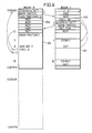
- Fig. 1 is a block diagram showing schematically the arrangement of the information processing apparatus which embodies the present invention.
- the inventive information processing apparatus includes a CPU 1 which is the core of the processor for implementing various computational and control operations, and a program memory 4 which is conformable to both direct and bank mappings.
- the CPU 1 has an address space of 1M (220) bytes, for example, and provides the 20-bit address A0 - A19 on an address bus 2.
- the program memory 4 is comprised of a ROM accessible by the 16-bit address MA0 - MA15, i.e., having a capacity of 64K (216) bytes, and it stores, for example, the Basic I/O System (BIOS) that is a control program for input/output units and disk drivers.
- BIOS Basic I/O System
- ROM program memory
- an address decoder 7 which controls enabling and disabling of the output of the ROM 4
- bank registers 5 and 6 and associated address decoders 8 and 9 for designating banks of the ROM 4
- switching circuit 10 which selectively sets direct scheme or bank scheme for mapping the memory area of the ROM 4 in the address space of the CPU 1.
- the address decoders 8 and 9 receive the high-order 6 address bits A14 - A19, for example, provided by the CPU 1 over the address bus 2, and produce an active signal of "1", if the received 6-bit address indicates a location within a predetermined address area and the CPU 1 issues a write signal W.
- the bank registers 5 and 6 are each formed of a D-type flip-flop, for example, having a clock input CK, data input D and data output Q.
- the bank register 5 responds to the active output of the address decoder 8 to latch data D1 on the data bus 3 and to release it as output data through its output terminal Q.
- the bank register 6 responds to the active output of the address decoder 9 to latch data D0 on the data bus 3 and to release it as output data through its output terminal Q.
- the 2 data bits D0 and D1 designate one of four memory blocks (will be mentioned in the below) of the ROM 4.
- the switching circuit 10 includes switches 11, 12 and 13 of hardware implementation for example.
- the switch 11 has an input terminal B receiving the address bit A14 on the address bus 2 and an input terminal C connected to the ground, and delivers its output to the address decoder 7.
- the switch 12 has an input terminal B receiving the Q output of the bank register 5 and an input terminal C connected to a predetermined supply voltage Vcc, and provides its output to the highest address bit MA15 input of the ROM 4.
- the switch 13 has an input terminal B receiving the output Q of the bank register 5 and an input terminal C receiving the address bit A14, and provides its output to the next highest address bit MA14 input of the ROM 4.
- the address decoder 7 receives high-order address bits A15 to A17 from the CPU 1 through the address bus 2 and also receives the output of the switch 11.
- the address decoder 7 produces a "0" signal when the high-order address bits A16 - A19 from the CPU 1 is "C" in hexadecimal or "1100" in binary and the two address bits A14 - A15 are both "0", enabling the ROM 4 to output.
- the reason for setting the address A16 - A19 to the hexadecimal C is that the ROM 4 of the instant embodiment stores, for example, the BIOS mentioned previously and within the segment COOOH of CPU 1 is assigned the BIOS area. Accordingly, if the ROM 4 is assigned to other segment of the CPU 1, the address decoder 7 will provide a different value of address bits A16 - A19 for bringing the ROM 4 into the output enabled state.
- the ROM 4 has an address space of OOOOH-FFFFH (H : hexadecimal and it is divided into four memory blocks 14, 15, 16 and 17 each having a 16 K (214) byte capacity.
- the first memory block 14 occupies the address area OOOOH-3FFFH of ROM 4, the second memory block 15 is assigned to the area 4000H-7FFFH, the third memory block 16 is to the area 8000H-BFFFH, and the fourth memory block 17 is to the area of COOOH-FFFFH.
- the first program 100 used in bank mapping is stored in the first and second memory blocks 14 and 15, and the second program used in memory blocks 14 and 15, and the second program used in direct mapping is stored in the third and fourth memory blocks 16 and 17.
- One memory bank is of 16 K bytes in bank mapping.
- first program 100 and second program 200 are virtually the same in the content of process, the first program 100 for bank scheme differs from the second program for direct scheme in the additional inclusion of a bank switching control program for the bank switching between the first memory block 14 and second memory block 15.
- Fig. 3 shows an example of the first program 100, the specific content of which is disclosed in detail in the copending U.S. Patent Application Serial No. filed by the same applicant.
- Fig. 3 shows the content of program of the case in which a main routine stored in the first memory block 14 calls a subroutine stored in the second memory block 15.
- the memory bank switching control program is stored in the same address area 110 (hexadecimal 0000-Z of ROM 4 in Fig. 3) of the first and second memory blocks 14 and 15.
- main routine of the first memory block 14 In order for main routine of the first memory block 14 to call a subroutine (SUB1) stored in the second memory block 15, it is appended with instruction MOV BX, Y for transferring starting address y of the subroutine SUB1 relative to the ROM 4 to a register BX (incorporated in the CPU 1), and instruction CALL 0 for invoking the bank switching control program in the first memory block 14.
- the bank switching control program in the memory block 14 includes the bank switching instruction, instruction NOP, and return instruction RET for returning to the main routine.
- the second memory block 15 includes plural kinds of subroutines SUB1 and SUB2, and the bank switching control program.
- the bank switching control program in the second memory block 15 includes the instruction NOP, instruction CALL BX for invoking the content starting at the address stored in register BX (i.e., calling a subroutine), and the bank switching program.
- the operation of the first program will be explained in brief in the following, for the case as an example when the subroutine SUB1 in the second memory block 15 needs to be invoked during execution of the main routine stored in the first memory block 14.
- starting address Y of the subroutine SUB1 is transferred to the register BX.
- the bank switching control program in the first memory block 14 is called by instruction CALL 0, and the memory bank is switched from the first memory block 14 to the second memory block 15 (bank switching operation will be explained later).
- the subroutine SUB1 beginning at address Y is called by instruction CALL BX in the bank switching control program in the second memory block 15, and it is executed.
- the RET instruction transfers control back to the bank switching control program in the second memory block 15 so that the bank is switched from the second memory block 15 to the first memory block 14. Subsequently, the RET instruction of the bank switching control program in the first memory block 14 brings the process back to the main routine.
- address W is transferred to the register BX at address X of the main routine.
- the address area 110 shown in Fig. 3 is extended so that the bank switching control program from the second memory block 15 to the first memory block 14 is stored in the extended area.
- the address decoder 7 receives address bits A16 - A19 and A15 and the "0" bit from the switch 11. The address decoder 7 enables the ROM 4 to output only when the address bit A15 is "0" and the address bits A16 - A19 are equal to hexadecimal C. Accordingly, the contents of ROM 4 are mapped in the address space C0000H-C7FFFH where the address bit A15 is "0" in the segment C of CPU 1. Since the ROM 4 has its most significant address bit MA15 fixed to "1", it has the address area of 80000H-FFFFH be accessible. Consequently, as shown in Fig. 4, the third and fourth memory blocks 16 and 17, i.e., the second program 200, are mapped directly to the address area of C0000H-C7FFFH of CPU 1.
- the ROM 4 With all input terminals of the switches 11 - 13 in the switching circuit 10 being set to the B-input position, the ROM 4 has its address bits MA15 and MA14 receive the outputs of the bank registers 5 and 6, respectively, and the address decoder 7 receives directly the address bits A14 and A15 from the CPU 1. Consequently, as shown in Fig. 5, the first through fourth memory blocks 14 - 17 of ROM 4 are mapped as memory banks 0 - 3 in the address area C0000H-C3FFFH, where the address bits A14 and A14 are both "0", in the address area C0000H-CFFFH of the CPU 1.
- the memory blocks of ROM 4 are selected by the most significant address bits MA14 and A15 provided by the bank registers 5 and 6, i.e., 2-bit data D0 and D1 from the CPU 1.
- data (D1, D0) being (0, 0)
- the first memory block (bank 0) 14 is designated, with (0, 0)
- the second memory block (bank 1) 15 is designated, with (1, 0)
- the third memory block (bank 2) 16 is designated
- (1, 1), the fourth memory block (bank 3) is designated.
- bank switching is carried out by the CPU 1 which sets the bank designation data D0 and D1 to the bank registers 5 and 6 in accordance with the bank switching control program included in the first program 100. More specifically, the bank switching takes place as follows. In the bank designation, the CPU 1 places the bank designation data D0 and D1 on the data bus 3, and thereafter issues a set of predetermined values of address bits A14 - A19 (e.g., 110000) to the address decoders 8 and 9 and further issues the write signal W thereto. The address decoders 8 and 9 respond to the address bits A14 -A19 and the write signal W to provide an active signal to the clock input CK of the bank registers 5 and 6.
- a set of predetermined values of address bits A14 - A19 e.g., 110000
- the bank registers 5 and 6 latch the data on the data bus 3.
- the values of address which causes the address decoders 8 and 9 to produce active signals should be set so that the decoders 8 and 9 respond only when a memory bank within address range C0000H-C3FFFH is accessed, thereby avoiding possible unnecessary rewriting of the bank registers 5 and 6.
- the bank registers 5 and 6 are both initialized to have Q output "1" when power is turned on, and therefore the fourth memory block (bank 3) 17 is selected as the memory bank initially. Consequently, the bank switch command to the first memory block 14 is stored in address COOOH (relative to ROM 4) of the fourth memory block 17. By this bank switching command, the bank is switched to the first memory block (memory bank 0) 14 under control of the CPU 1, followed by the execution of the initialization routine and then the prescribed process by the first program which has been mapped as bank 0 and bank 1. It should be noted that address C000H of the fourth memory block (memory bank 3) 17 is unnecessary at the execution of the second processing program 200, and on this account the second program 200 is designed so that the address C000H is not used at the execution of the second program 200.
- a single ROM is used as the program memory 4, in which the first and second programs are stored.
- the first and second programs may be stored in separate ROMS, and furthermore each memory block may be arranged in each individual ROM.
- the information processing apparatus includes a CPU 1, a program memory 40, a bank register 70, address decoders 80 and 90, and a switching circuit 105.
- the CPU 1 has an address space of 1 M bytes (220 bytes ranging 00000H-FFFFFH, for example, and provides 20-bit address A0 - A19 on the address bus 2.
- the program memory 40 is arranged in a 32 K(215) byte ROM, including a first memory block 50 of 16 K bytes ranging 0000H-3FFFH and a second memory block 60 of 16 K bytes ranging 4000H-7FFFH, as shown schematically in Fig.
- the first memory block 50 stores the first processing program
- the second memory block 60 stores the second processing program.
- the first and second processing programs in unison form a control program such as BIOS.
- the address decoder 80 serves to decode the high-order 6 address bits A14 - A19, for example, on the address bus 2, and only when the given address is within a predetermined area, it provides an active signal to the clock input CK of the bank register 70 in response to the write signal W.
- the bank register 70 responds to the active input at its clock input CK to latch the bank designation data D0 on the data bus 3 and to release the latched data as output Q.
- the switching circuit 105 selects either direct scheme or bank scheme as a scheme for mapping the contents of program memory 40 in the address space of CPU 1.
- the switching circuit 105 includes switches 111 and 112.
- the switch 111 has an input terminal B receiving an address bit A14 from the CPU 1 and an input terminal C connected to the ground, while the switch 112 has an input terminal B receiving the Q output from the bank register 70 and an input terminal C receiving the address bit A14 from the CPU 1.
- the address decoder 90 receives 5 address bits A15 -A19 from the CPU 1 and the output of the switch 111, and delivers its output to the output enable terminal OE of the program memory 40.
- the address decoder 90 produces an active enable signal ("0" level in Fig. 6) only when the address A16 - A19 from the CPU 1 is hexadecimal C, for example, and at the same time the address bit A15 and the output of switch 111 are both "0".
- the program memory 40 has its address designated by the output of the switch 112 and the address A0 - A13 from the CPU 1. The output of the switch 112 is given to the most significant address bit MA14 of the program memory 40.
- the bank mapping scheme is selected by setting the input terminals of the switches 111 and 112 to the respective B input position.
- the contents of the program memory 40 are mapped as a memory bank in the address area in which the address A16 - A19 is hexadecimal C and address bits A14 and A15 are both "0", i.e., in the area C0000H-C3FFFH of CPU address space.
- the most significant address bit MA14 of the program memory 40 When the most significant address bit MA14 of the program memory 40 is "0", the first memory block 50 in the address area 0000H-3FFFH of the program memory 40 is selected as bank 0, and when the most significant address bit MA14 is "1", the second memory block 60 in the address area 4000H-7FFFH of the program memory 40 is selected as bank 1.
- direct mapping scheme is selected.
- the whole contents of program memory 40 i.e., the first and second memory blocks 50 and 60
- the address bit A14 of CPU 1 is supplied to the most significant address bit MA14 of the program memory 40 through the switch 112, and the first memory block 50 is mapped in the address area C0000H-3FFFFH of CPU 1, and the second memory block 60 is mapped in the address area C4000H-C7FFFH of CPU 1.
- the first and second processing programs stored in the first memory block 50 and second memory block 60, respectively, is designed to have the contents as shown specifically for example in Fig. 8 and 9, so that both of direct scheme and bank scheme can be compatibly used. Shown in Figs. 8 and 9 are examples in which the main routine of the first processing program invokes the subroutines of the second processing program.
- the first and second memory blocks 50 and 60 store the first and second control programs 130 and 140 in the respective starting addresses 0000H and 4000H through a relative address Z.
- Mapping scheme identification information "JA" is stored in the specific address (4000H in Figs. 8 and 9) of the second memory block 60.
- the "CALL FAR C400 : 4" instruction is to call and execute the contents beginning at the address C4004H which is the starting address C4000H added by the offset address 4.
- the "RET FAR” instruction is to shift the execution address (address to be executed) to the address next to the address where the "CALL FAR” instruction is stored.
- the instructions “CALL FAR C400 : 4" and "RET FAR” are to merely shift the execution address in the address space of CPU 1 in the direct mapping scheme.
- Figs. 8 and 9 the operation in the case in which the main routine in the first processing program calls a subroutine in the second processing program to execute it.
- the addresses X, Y, Z and W represent offset addresses from the starting address C0000H or C40000H of each segment (each memory block). Arrows in the figures indicates the progression of operation.
- the first and second control programs are stored with their addresses being correspondent mutually so that the address counter does not be revised unnecessary at each instruction execution.
- the operation in direct mapping scheme will first be explained with reference to Fig. 8.
- the first memory block 50 is mapped in CPU's address space C0000H-C3FFFH
- the second memory block 60 is mapped in C4000H-C7FFFH thereof. Accordingly, the identification information "JA" is stored in the specific address C4000H of the CPU's address space.
- the starting address Y of the subroutine SUB1 is transferred to the register BX (incorporated in CPU 1).
- the first control program 130 is executed by the instruction "CALL 0".
- the command at the top address C0000H of the first control program 130 decides whether or not the identification information "JA" is stored in address C4000H of CPU 1.
- the decision result is "yes" in this direct mapping scheme. Accordingly, the bank switching instruction stored in the next address is skipped.
- the instruction "CALL FAR C400 : 4" at the skipped destination address causes the execution program to make transition from the first processing program to the second processing program, and then the instruction "CALL BX" at address C4004H is executed as shown by the arrow in Fig. 8.
- the register BX is already supplied with the starting address Y of the subroutine SUB1 by the main routine of the first processing program. Then, the subroutine SUB1 is invoked by the CALL instruction and it is executed. On completion of execution of the subroutine SUB1, the RET instruction in the subroutine SUB1 causes the execution address to move to the decision step of identification information in the second processing program.
- the RET FAR instruction is executed, and the program sequence returns to the first control program 130. Namely, the execution program makes a transition from the second processing program to the first processing program. Subsequently, through the execution of the RET instruction in the first control program 130, the sequence returns to the main routine of the first processing program. It should be noted that if it is intended to call and execute the subroutine SUB2 from the main routine, the subroutine starting address W is stored in the register BX.
- the switches 111 and 112 have their input terminals set to the B input position. Consequently, the first and second memory blocks 50 and 60 are mapped as bank 0 and bank 1 in the address area C0000H-C3FFFH in the address space of CPU 1. Accordingly, the identification information "JA" is not stored in the specific address C4000H of CPU 1. Therefore, when the main routine of the first processing program has invoked the first control program 130, the decision step for identification information results in "no", and the bank switching instruction is executed.
- the bank switching instruction sets the bank register 70 to store "1" under control of CPU 1, and the memory bank is switched from bank 0 to bank 1, followed by the transition from the first processing program to the second processing program.
- the CALL BX instruction in the second control program 140 of the second processing program calls and executes the subroutine SUB1 beginning at the address Y stored in the register BX.
- the RET instruction in the subroutine SUB1 brings the program sequence back to the second control program 140.
- Return to the second control program 140 is immediately followed by the decision on identification information.
- the decision result is "no" in this case, and the bank switching instruction stored in the next address is executed.
- the bank switching takes place in the manner of setting in the bank register 70 "0" under control of CPU 1.
- the transition from the second processing program to the fist processing program is carried out, and then the first control program 130 is executed.
- the RET instruction in the first control program 130 brings the program sequence back to the main routine of the first processing program, and the execution of main routine is resumed at address X + 2.
- mapping schemes are readily accomplished by switching the input terminals of the switches 111 and 112 in the switching circuit 105.
- the second and first control programs are added to the first and second control programs as shown in Figs. 8 and 9, respectively.
- Any decoder configuration may be employed as far as the following requirement is satisfied.
- one is designed to produce an active enable signal when the address A16 - A19 is hexadecimal C and at the same time the address bit A15 is "0" (address bit A14 may be any), and the other is to produce an active enable signal when the address A16 - A19 is hexadecimal C and at the same time address bits A14 and A15 both are "0".
- each processing program may be stored in two or more ROMs.
- each memory block In the case of using two ROM chips, replacing the most significant address bits MA14 of ROM 40 in Fig. 6 with the chip enable signal CE allows each memory block to be readily mapped in any of bank mapping scheme and direct mapping scheme.
- the structure may be also employed in which the output of the switch 112 and the output of the address decoder 90 in Fig. 6 is subjected to such a logical operation as OR or NOR corresponding to each memory block and then applied to the output enable terminal of ROM.
- each ROM has its number of address bits decreased as the number of ROMs increases, and, by logically processing the remaining address bits from the CPU 1 appropriately, the ROM memory blocks can readily be mapped in the address space of CPU 1 according to each mapping scheme.
- a program which is designed to deal with both of the bank and direct schemes is stored in the program memory, and therefore the information processing apparatus can deal with any of the direct mapping scheme and bank mapping scheme by merely switching the mapping scheme on a hardware basis, instead of replacing the program memory.
Abstract
Description
- The present invention relates to an information processing apparatus such as a personal computer, and particularly to an apparatus and method, intended for an information processing apparatus having a plurality of memory blocks each storing a processing program, for mapping the processing programs in the address space of a central processing unit (CPU) based on either direct scheme or bank scheme.
- Recently, information processors such as personal computers and word processors are used in extensive fields. Such an information processing apparatus is provided with a ROM-based (ROM : read only memory) program memory for fixedly storing a system program which determines the fundamental operational function of the information processing apparatus. The program memory is generally mapped directly in the CPU address space.
- However, for an information processing apparatus which is constrained in its standard memory capacity from the viewpoint of price/performance factor and the like, when it is intended to set as wide user-accessible memory space (CPU address space) as possible, the address area assigned to the program memory is restricted, and a complete application program for providing a desired function cannot be stored therein. In such cases, bank scheme as disclosed in, for example, Japanese Patent Unexamined Publication No. 120543/1987 is adopted. In bank scheme, a program memory is formed of multiple memory blocks, with each memory block being mapped on the same address area in the CPU's address space.
- As one example, a case is considered in which the CPU's address space has an optional area, for storing an application dependent content assigned in proximity to the program area. In this case, if a user wants to load an optional software (program), its program memory area is confined in a predetermined address area since the CPU's address space is fixed. Therefore, in order to store the whole of a program which exceeds the limited capacity of the program memory area, it must be mapped on the basis of bank scheme.
- On the other hand, if no optional software needs to be loaded, that area can be used as an extended program memory area, and in this case the program memory area can be acquired through the usual direct mapping instead of bank scheme.
- However, in order for a program conformable to bank scheme to process a routine across different memory banks, it needs to switch banks. Due to some differences in program between bank scheme and direct scheme, two types of programs must be prepared. Moreover, bank scheme which inevitably includes the bank switching step is slower in processing speed than the direct scheme.
- It is desirable for a processor to have the ability of selecting a mapping scheme depending on whether an application involves optional software. To this end, a recent proposed hardware scheme is capable of selecting either direct or bank mapping for the memory blocks of program memory by use of a jumper wire or hardware switch (or memory switch). Information processors with the above-mentioned hardware arrangement have a mapping scheme selected through selective connection by a jumper wire or switch, and have a program memory mounted selectively or replaced from among two kinds of program memories prepared in advance for direct and bank schemes. On this account, switching of mapping schemes necessitates a hardware modification using a jumper wire or switch, as well as replacement of the program memories for the alternation of software. Moreover, because both of these two mapping schemes cannot be accomplished by a single program memory, two types of programs would be required for the two mapping schemes. However, the provision of two kinds of program memories is unfavorable from the viewpoints of working efficiency and maintainability.
- An object of this invention is to provide an improved information processing apparatus which readily deals with both direct scheme and bank scheme.
- Another object of this invention is to provide an information processing apparatus which can deal with both bank scheme and direct scheme by merely switching the mapping schemes on a hardware basis.
- A further object of this invention is to provide an information processing apparatus having a program memory which is in turn conformable with both direct and bank mapping schemes.
- A further object of this invention is to provide a program memory based on the program transition scheme which can deal with both direct and bank mapping schemes.
- A further object of this invention is to provide a program memory based ont he program transition scheme which can deal with both direct and bank schemes using only one kind of program.
- A further object of this invention is to provide a program memory based on the program transition scheme which can deal with both direct and bank mapping schemes without program alternation.
- A further object of this invention is to provide a program execution method which can deal with both direct and bank mapping schemes without program memory replacement.
- The information processing apparatus of this invention comprises a program memory for storing a program which can deal with both of bank mapping scheme and direct mapping scheme, and means for selectively setting either direct mapping scheme or bank mapping scheme and mapping the memory address of the program memory in an address space of a central processing unit (CPU) included in the information processing apparatus, in accordance with the selected mapping scheme.
- According to a first aspect of this invention, the program memory includes a first memory block which stores a first program having the content of processing corresponding to bank mapping scheme, and a second memory block which stores a second program having the content of processing corresponding to direct mapping scheme. The second program is substantially the same in the processing content as the first program except for the exclusion of a program for bank switching.
- According to a second aspect of this invention, the program memory includes a third memory block which stores a first processing program, and a fourth memory block which stores a predetermined identification information in a specific memory address and a second processing program. The information processing apparatus having the program memory according to the second aspect includes means for, during execution of the first and second processing programs, making decision as to whether the identification information is stored in the address to which the above-mentioned specific memory address corresponds when the fourth memory block is mapped in direct mapping scheme in the CPU's address space in the direct mapping scheme and for implementing the switching of memory banks or the transition of address to be executed in the CPU's address space.
- In the case of using a program memory according to the first aspect, the second program is executed when the direct mapping scheme is selected, while the first program is executed when the bank mapping scheme is selected.
- In the case of using a program memory according to the second aspect, the identification information is surely stored in the correspondent address in the CPU's address space when direct mapping scheme is selected, while in bank mapping scheme the identification information is not stored in the correspondent address therein. Accordingly, through the judgement as to whether the identification information is present in the above-mentioned correspondent address, the transition scheme between the first processing program and the second processing program can be selected depending on the mapping scheme. Consequently, the mapping scheme can be switched without replacing the program memory.
- These and other objects and features of this invention will become more apparent from the following detailed description taken in conjunction with the accompanying drawings.
-
- Fig. 1 shows schematically the arrangement of the information processing apparatus of an embodiment according to the invention;
- Fig. 2 shows an example of the arrangement of the program memory shown in Fig. 1;
- Fig. 3 shows an exemplary specific content of the first program shown in Fig. 2;
- Fig. 4 shows the layout of memory blocks of the program memory in the CPU address space when the program memory shown in Fig. 2 has been mapped in direct scheme in the CPU's address space;
- Fig. 5 shows the layout of memory block of the program memory in the CPU address space when the program memory shown in Fig. 2 is mapped in bank scheme in the CPU's address space;
- Fig. 6 shows schematically the arrangement of the information processing apparatus of another embodiment according to this invention;
- Fig. 7 shows schematically the arrangement of the program memory shown in Fig. 6;
- Fig. 8 shows schematically the layout of memory blocks of the program memory in the CPU's address space when the program memory shown in Fig. 7 is mapped in direct scheme in the CPU's address space, and also shows the content of program stored in each memory block and the operation flow; and
- Fig. 9 shows specifically the layout of memory blocks of the program memory in the CPU's address space when the program memory shown in Fig. 7 is mapped in back mapping in the CPU's address space, as well as the operation flow.
- Fig. 1 is a block diagram showing schematically the arrangement of the information processing apparatus which embodies the present invention. The inventive information processing apparatus includes a
CPU 1 which is the core of the processor for implementing various computational and control operations, and aprogram memory 4 which is conformable to both direct and bank mappings. TheCPU 1 has an address space of 1M (2²⁰) bytes, for example, and provides the 20-bit address A0 - A19 on anaddress bus 2. Theprogram memory 4 is comprised of a ROM accessible by the 16-bit address MA0 - MA15, i.e., having a capacity of 64K (2¹⁶) bytes, and it stores, for example, the Basic I/O System (BIOS) that is a control program for input/output units and disk drivers. - For switching of the memory area configuration of the program memory (which will be termed simply "ROM" hereinafter) 4 in correspondence to direct mapping scheme or bank mapping scheme, there are provided an address decoder 7 which controls enabling and disabling of the output of the
ROM 4,bank registers 5 and 6 and associatedaddress decoders ROM 4, and aswitching circuit 10 which selectively sets direct scheme or bank scheme for mapping the memory area of theROM 4 in the address space of theCPU 1. - The
address decoders CPU 1 over theaddress bus 2, and produce an active signal of "1", if the received 6-bit address indicates a location within a predetermined address area and theCPU 1 issues a write signal W. - The
bank registers 5 and 6 are each formed of a D-type flip-flop, for example, having a clock input CK, data input D and data output Q. Thebank register 5 responds to the active output of theaddress decoder 8 to latch data D1 on thedata bus 3 and to release it as output data through its output terminal Q. The bank register 6 responds to the active output of theaddress decoder 9 to latch data D0 on thedata bus 3 and to release it as output data through its output terminal Q. The 2 data bits D0 and D1 designate one of four memory blocks (will be mentioned in the below) of theROM 4. - The
switching circuit 10 includesswitches switch 11 has an input terminal B receiving the address bit A14 on theaddress bus 2 and an input terminal C connected to the ground, and delivers its output to the address decoder 7. The switch 12 has an input terminal B receiving the Q output of thebank register 5 and an input terminal C connected to a predetermined supply voltage Vcc, and provides its output to the highest address bit MA15 input of theROM 4. Theswitch 13 has an input terminal B receiving the output Q of thebank register 5 and an input terminal C receiving the address bit A14, and provides its output to the next highest address bit MA14 input of theROM 4. - The address decoder 7 receives high-order address bits A15 to A17 from the
CPU 1 through theaddress bus 2 and also receives the output of theswitch 11. - The address decoder 7 produces a "0" signal when the high-order address bits A16 - A19 from the
CPU 1 is "C" in hexadecimal or "1100" in binary and the two address bits A14 - A15 are both "0", enabling theROM 4 to output. The reason for setting the address A16 - A19 to the hexadecimal C is that theROM 4 of the instant embodiment stores, for example, the BIOS mentioned previously and within the segment COOOH ofCPU 1 is assigned the BIOS area. Accordingly, if theROM 4 is assigned to other segment of theCPU 1, the address decoder 7 will provide a different value of address bits A16 - A19 for bringing theROM 4 into the output enabled state. - The
ROM 4 has an address space of OOOOH-FFFFH (H : hexadecimal and it is divided into fourmemory blocks first memory block 14 occupies the address area OOOOH-3FFFH ofROM 4, thesecond memory block 15 is assigned to thearea 4000H-7FFFH, thethird memory block 16 is to thearea 8000H-BFFFH, and thefourth memory block 17 is to the area of COOOH-FFFFH. Thefirst program 100 used in bank mapping is stored in the first and second memory blocks 14 and 15, and the second program used in memory blocks 14 and 15, and the second program used in direct mapping is stored in the third and fourth memory blocks 16 and 17. One memory bank is of 16 K bytes in bank mapping. - Although the
first program 100 andsecond program 200 are virtually the same in the content of process, thefirst program 100 for bank scheme differs from the second program for direct scheme in the additional inclusion of a bank switching control program for the bank switching between thefirst memory block 14 andsecond memory block 15. - Fig. 3 shows an example of the
first program 100, the specific content of which is disclosed in detail in the copending U.S. Patent Application Serial No. filed by the same applicant. Fig. 3 shows the content of program of the case in which a main routine stored in thefirst memory block 14 calls a subroutine stored in thesecond memory block 15. Referring to Fig. 3 the memory bank switching control program is stored in the same address area 110 (hexadecimal 0000-Z ofROM 4 in Fig. 3) of the first and second memory blocks 14 and 15. In order for main routine of thefirst memory block 14 to call a subroutine (SUB1) stored in thesecond memory block 15, it is appended with instruction MOV BX, Y for transferring starting address y of the subroutine SUB1 relative to theROM 4 to a register BX (incorporated in the CPU 1), and instruction CALL 0 for invoking the bank switching control program in thefirst memory block 14. The bank switching control program in thememory block 14 includes the bank switching instruction, instruction NOP, and return instruction RET for returning to the main routine. - The
second memory block 15 includes plural kinds of subroutines SUB1 and SUB2, and the bank switching control program. The bank switching control program in thesecond memory block 15 includes the instruction NOP, instruction CALL BX for invoking the content starting at the address stored in register BX (i.e., calling a subroutine), and the bank switching program. The operation of the first program will be explained in brief in the following, for the case as an example when the subroutine SUB1 in thesecond memory block 15 needs to be invoked during execution of the main routine stored in thefirst memory block 14. - At address X of the
first memory block 14, starting address Y of the subroutine SUB1 is transferred to the register BX. At address X+1, the bank switching control program in thefirst memory block 14 is called by instruction CALL 0, and the memory bank is switched from thefirst memory block 14 to the second memory block 15 (bank switching operation will be explained later). Then, the subroutine SUB1 beginning at address Y is called by instruction CALL BX in the bank switching control program in thesecond memory block 15, and it is executed. Upon completion of the execution of subroutine SUB1, the RET instruction transfers control back to the bank switching control program in thesecond memory block 15 so that the bank is switched from thesecond memory block 15 to thefirst memory block 14. Subsequently, the RET instruction of the bank switching control program in thefirst memory block 14 brings the process back to the main routine. - In calling the subroutine SUB2, address W is transferred to the register BX at address X of the main routine. When a processing program resident in the
second memory block 15 needs a subroutine in thefirst memory block 14, theaddress area 110 shown in Fig. 3 is extended so that the bank switching control program from thesecond memory block 15 to thefirst memory block 14 is stored in the extended area. - Next, the operation of the processor shown in Fig. 1 will be described. Initially, all input terminals of the switches 11 - 13 of the switching
circuit 10 are set to each C-input position. Consequently, theROM 4 has its address bit MA15 set to "1" by the switch 12, and its address bit MA14 receive the address bit A14 from the CPU1 through theswitch 13. - The address decoder 7 receives address bits A16 - A19 and A15 and the "0" bit from the
switch 11. The address decoder 7 enables theROM 4 to output only when the address bit A15 is "0" and the address bits A16 - A19 are equal to hexadecimal C. Accordingly, the contents ofROM 4 are mapped in the address space C0000H-C7FFFH where the address bit A15 is "0" in the segment C ofCPU 1. Since theROM 4 has its most significant address bit MA15 fixed to "1", it has the address area of 80000H-FFFFH be accessible. Consequently, as shown in Fig. 4, the third and fourth memory blocks 16 and 17, i.e., thesecond program 200, are mapped directly to the address area of C0000H-C7FFFH ofCPU 1. - With all input terminals of the switches 11 - 13 in the switching
circuit 10 being set to the B-input position, theROM 4 has its address bits MA15 and MA14 receive the outputs of the bank registers 5 and 6, respectively, and the address decoder 7 receives directly the address bits A14 and A15 from theCPU 1. Consequently, as shown in Fig. 5, the first through fourth memory blocks 14 - 17 ofROM 4 are mapped as memory banks 0 - 3 in the address area C0000H-C3FFFH, where the address bits A14 and A14 are both "0", in the address area C0000H-CFFFH of theCPU 1. The memory blocks ofROM 4 are selected by the most significant address bits MA14 and A15 provided by the bank registers 5 and 6, i.e., 2-bit data D0 and D1 from theCPU 1. With data (D1, D0) being (0, 0), the first memory block (bank 0) 14 is designated, with (0, 0), the second memory block (bank 1) 15 is designated, with (1, 0), the third memory block (bank 2) 16 is designated, and with (1, 1), the fourth memory block (bank 3) is designated. - In bank mapping, the bank switching is carried out by the
CPU 1 which sets the bank designation data D0 and D1 to the bank registers 5 and 6 in accordance with the bank switching control program included in thefirst program 100. More specifically, the bank switching takes place as follows. In the bank designation, theCPU 1 places the bank designation data D0 and D1 on thedata bus 3, and thereafter issues a set of predetermined values of address bits A14 - A19 (e.g., 110000) to theaddress decoders address decoders address decoders data bus 3. In this case, the values of address which causes theaddress decoders decoders - In the foregoing embodiments, the bank registers 5 and 6 are both initialized to have Q output "1" when power is turned on, and therefore the fourth memory block (bank 3) 17 is selected as the memory bank initially. Consequently, the bank switch command to the
first memory block 14 is stored in address COOOH (relative to ROM 4) of thefourth memory block 17. By this bank switching command, the bank is switched to the first memory block (memory bank 0) 14 under control of theCPU 1, followed by the execution of the initialization routine and then the prescribed process by the first program which has been mapped as bank 0 andbank 1. It should be noted that address C000H of the fourth memory block (memory bank 3) 17 is unnecessary at the execution of thesecond processing program 200, and on this account thesecond program 200 is designed so that the address C000H is not used at the execution of thesecond program 200. - In the foregoing embodiment, a single ROM is used as the
program memory 4, in which the first and second programs are stored. However, the first and second programs may be stored in separate ROMS, and furthermore each memory block may be arranged in each individual ROM. - Although in the foregoing embodiment two kinds of programs i.e., the first and second programs are prepared and only one of them is used depending on the mapping scheme, an alternative way is to deal with both of direct mapping and bank mapping using only one kind of program, as shown schematically in Fig. 6 as another embodiment of this invention.
- Referring to Fig. 6, the information processing apparatus according to another embodiment includes a
CPU 1, aprogram memory 40, abank register 70,address decoders switching circuit 105. TheCPU 1 has an address space of 1 M bytes (2²⁰ bytes ranging 00000H-FFFFFH, for example, and provides 20-bit address A0 - A19 on theaddress bus 2. - The
program memory 40 is arranged in a 32 K(2¹⁵) byte ROM, including afirst memory block 50 of 16 K bytes ranging 0000H-3FFFH and asecond memory block 60 of 16 K bytes ranging 4000H-7FFFH, as shown schematically in Fig. - 7. The
first memory block 50 stores the first processing program, and thesecond memory block 60 stores the second processing program. The first and second processing programs in unison form a control program such as BIOS. - The
address decoder 80 serves to decode the high-order 6 address bits A14 - A19, for example, on theaddress bus 2, and only when the given address is within a predetermined area, it provides an active signal to the clock input CK of thebank register 70 in response to the write signal W. Thebank register 70 responds to the active input at its clock input CK to latch the bank designation data D0 on thedata bus 3 and to release the latched data as output Q. - The
switching circuit 105 selects either direct scheme or bank scheme as a scheme for mapping the contents ofprogram memory 40 in the address space ofCPU 1. Theswitching circuit 105 includesswitches 111 and 112. The switch 111 has an input terminal B receiving an address bit A14 from theCPU 1 and an input terminal C connected to the ground, while theswitch 112 has an input terminal B receiving the Q output from thebank register 70 and an input terminal C receiving the address bit A14 from theCPU 1. - The
address decoder 90 receives 5 address bits A15 -A19 from theCPU 1 and the output of the switch 111, and delivers its output to the output enable terminalOE of theprogram memory 40. Theaddress decoder 90 produces an active enable signal ("0" level in Fig. 6) only when the address A16 - A19 from theCPU 1 is hexadecimal C, for example, and at the same time the address bit A15 and the output of switch 111 are both "0". Theprogram memory 40 has its address designated by the output of theswitch 112 and the address A0 - A13 from theCPU 1. The output of theswitch 112 is given to the most significant address bit MA14 of theprogram memory 40. - Although the foregoing arrangement resembles the one shown in Fig. 1, only one program is stored in the
program memory 40, and the arrangement is simpler than that of Fig. 1. The operation of designating the mapping scheme is virtually the same as that of Fig. 1, and therefore only a brief explanation will be given in the foregoing. - The bank mapping scheme is selected by setting the input terminals of the
switches 111 and 112 to the respective B input position. In this case, as shown in Fig. 9, the contents of theprogram memory 40 are mapped as a memory bank in the address area in which the address A16 - A19 is hexadecimal C and address bits A14 and A15 are both "0", i.e., in the area C0000H-C3FFFH of CPU address space. When the most significant address bit MA14 of theprogram memory 40 is "0", thefirst memory block 50 in theaddress area 0000H-3FFFH of theprogram memory 40 is selected as bank 0, and when the most significant address bit MA14 is "1", thesecond memory block 60 in theaddress area 4000H-7FFFH of theprogram memory 40 is selected asbank 1. - With the input terminals of the
switches 111 and 112 being set to the respective C input positions, direct mapping scheme is selected. In this case, the whole contents ofprogram memory 40, i.e., the first and second memory blocks 50 and 60, are mapped directly in the address area C0000H-C7FFFH ofCPU 1, as shown in Fig. 8. At this time, the address bit A14 ofCPU 1 is supplied to the most significant address bit MA14 of theprogram memory 40 through theswitch 112, and thefirst memory block 50 is mapped in the address area C0000H-3FFFFH ofCPU 1, and thesecond memory block 60 is mapped in the address area C4000H-C7FFFH ofCPU 1. - The first and second processing programs stored in the
first memory block 50 andsecond memory block 60, respectively, is designed to have the contents as shown specifically for example in Fig. 8 and 9, so that both of direct scheme and bank scheme can be compatibly used. Shown in Figs. 8 and 9 are examples in which the main routine of the first processing program invokes the subroutines of the second processing program. - Referring to Figs. 8 and 9, the first and second memory blocks 50 and 60 store the first and
second control programs second memory block 60. - The
first control program 130 includes the bank switching instruction, instruction "(C4000∼)="JA"", instruction "CALL FAR C400 : 4", instruction RET, and instruction NOP. The "(C4000∼)="JA"" instruction is to determine the identification information "JA" is stored in address C4000H ofCPU 1. The CPU's address C4000H corresponds to address 4000H of theprogram memory 4 in the direct mapping scheme, and it corresponds to an address in a memory block other than the first and second memory blocks 50 and 60 in the bank mapping scheme. Accordingly, by executing the "(C4000∼)="JA"" instruction, the mapping scheme can be identified. The "CALL FAR C400 : 4" instruction is to call and execute the contents beginning at the address C4004H which is the starting address C4000H added by the offsetaddress 4. - The
second control program 140 includes instruction "CALL BX", instruction "(C4000∼)="JA"", bank switching instruction, instruction "RET FAR", and instruction NOP, in addition to the identification information "JA". The "RET FAR" instruction is to shift the execution address (address to be executed) to the address next to the address where the "CALL FAR" instruction is stored. In other words, the instructions "CALL FAR C400 : 4" and "RET FAR" are to merely shift the execution address in the address space ofCPU 1 in the direct mapping scheme. - The following describes in detail with reference to Figs. 8 and 9 the operation in the case in which the main routine in the first processing program calls a subroutine in the second processing program to execute it. In Figs. 8 and 9, the addresses X, Y, Z and W represent offset addresses from the starting address C0000H or C40000H of each segment (each memory block). Arrows in the figures indicates the progression of operation. The first and second control programs are stored with their addresses being correspondent mutually so that the address counter does not be revised unnecessary at each instruction execution.
- The operation in direct mapping scheme will first be explained with reference to Fig. 8. In this case, as mentioned previously, the
first memory block 50 is mapped in CPU's address space C0000H-C3FFFH, and thesecond memory block 60 is mapped in C4000H-C7FFFH thereof. Accordingly, the identification information "JA" is stored in the specific address C4000H of the CPU's address space. - When execution of the first processing program progresses to reach the address X at which the subroutine SUB1 is to be called and executed, the starting address Y of the subroutine SUB1 is transferred to the register BX (incorporated in CPU 1). At the next address X + 1, the
first control program 130 is executed by the instruction "CALL 0". The command at the top address C0000H of thefirst control program 130 decides whether or not the identification information "JA" is stored in address C4000H ofCPU 1. The decision result is "yes" in this direct mapping scheme. Accordingly, the bank switching instruction stored in the next address is skipped. the instruction "CALL FAR C400 : 4" at the skipped destination address causes the execution program to make transition from the first processing program to the second processing program, and then the instruction "CALL BX" at address C4004H is executed as shown by the arrow in Fig. 8. The register BX is already supplied with the starting address Y of the subroutine SUB1 by the main routine of the first processing program. Then, the subroutine SUB1 is invoked by the CALL instruction and it is executed. On completion of execution of the subroutine SUB1, the RET instruction in the subroutine SUB1 causes the execution address to move to the decision step of identification information in the second processing program. Since the decision result is also "yes" in this scheme, the RET FAR instruction is executed, and the program sequence returns to thefirst control program 130. Namely, the execution program makes a transition from the second processing program to the first processing program. Subsequently, through the execution of the RET instruction in thefirst control program 130, the sequence returns to the main routine of the first processing program. It should be noted that if it is intended to call and execute the subroutine SUB2 from the main routine, the subroutine starting address W is stored in the register BX. - Next, the operation in bank mapping scheme will be explained with reference to Fig. 9. In this case, the
switches 111 and 112 have their input terminals set to the B input position. Consequently, the first and second memory blocks 50 and 60 are mapped as bank 0 andbank 1 in the address area C0000H-C3FFFH in the address space ofCPU 1. Accordingly, the identification information "JA" is not stored in the specific address C4000H ofCPU 1. Therefore, when the main routine of the first processing program has invoked thefirst control program 130, the decision step for identification information results in "no", and the bank switching instruction is executed. The bank switching instruction sets thebank register 70 to store "1" under control ofCPU 1, and the memory bank is switched from bank 0 tobank 1, followed by the transition from the first processing program to the second processing program. - After the transition of programs, the CALL BX instruction in the
second control program 140 of the second processing program calls and executes the subroutine SUB1 beginning at the address Y stored in the register BX. After the subroutine SUB1 has been executed, the RET instruction in the subroutine SUB1 brings the program sequence back to thesecond control program 140. Return to thesecond control program 140 is immediately followed by the decision on identification information. The decision result is "no" in this case, and the bank switching instruction stored in the next address is executed. The bank switching takes place in the manner of setting in thebank register 70 "0" under control ofCPU 1. As a result of the bank switching, the transition from the second processing program to the fist processing program is carried out, and then thefirst control program 130 is executed. The RET instruction in thefirst control program 130 brings the program sequence back to the main routine of the first processing program, and the execution of main routine is resumed ataddress X + 2. - As described above, both of bank mapping scheme and direct mapping scheme can be dealt with a single kind of program. The switching of mapping schemes is readily accomplished by switching the input terminals of the
switches 111 and 112 in theswitching circuit 105. - If the second processing program requires a subroutine in the first processing program, the second and first control programs are added to the first and second control programs as shown in Figs. 8 and 9, respectively.
- It is also possible to provide two respective address decoders for bank and direct mapping schemes in place of the switch 111 in the
switching circuit 105 and theaddress decoder 90 of the foregoing embodiment, wherein the outputs of the address decoders are delivered through a switch to the output enable terminal of theprogram memory 40. - Any decoder configuration may be employed as far as the following requirement is satisfied. Among the two address decoders one is designed to produce an active enable signal when the address A16 - A19 is hexadecimal C and at the same time the address bit A15 is "0" (address bit A14 may be any), and the other is to produce an active enable signal when the address A16 - A19 is hexadecimal C and at the same time address bits A14 and A15 both are "0".
- It is not always necessary for the first and second processing program to be stored in a single ROM, instead, each processing program may be stored in two or more ROMs.
- In the case of using two ROM chips, replacing the most significant address bits MA14 of
ROM 40 in Fig. 6 with the chip enable signalCE allows each memory block to be readily mapped in any of bank mapping scheme and direct mapping scheme. The structure may be also employed in which the output of theswitch 112 and the output of theaddress decoder 90 in Fig. 6 is subjected to such a logical operation as OR or NOR corresponding to each memory block and then applied to the output enable terminal of ROM. Also in the case of using three or more ROM chips, each ROM has its number of address bits decreased as the number of ROMs increases, and, by logically processing the remaining address bits from theCPU 1 appropriately, the ROM memory blocks can readily be mapped in the address space ofCPU 1 according to each mapping scheme. - The foregoing arrangement enables only one type of program to deal with both direct and bank mapping schemes, which not only eliminates the need of replacing the program memory itself depending on the mapping scheme, but also allows the use of a ROM of less capacity for the program memory. Moreover, it becomes unnecessary to prepare two programs of virtually the same content, and a significant improvement is achieved for the product cost, working efficiency and serviceability.
- According to the present invention, as described above, a program which is designed to deal with both of the bank and direct schemes is stored in the program memory, and therefore the information processing apparatus can deal with any of the direct mapping scheme and bank mapping scheme by merely switching the mapping scheme on a hardware basis, instead of replacing the program memory.
- Although the present invention has been described and illustrated in detail, it is clearly understood that the same is by way of illustration and example only and is not to be taken by way of limitation, the spirit and scope of the present invention being limited only by the terms of the appended claims.
Claims (24)
storage means (4) having a first memory block (14, 15) formed of a plurality of memory blocks for storing a first memory program (100) and a second memory block formed of at least one memory block for storing a second memory program (200), said first program being substantially the same in processing content as said second program excluding that said first program includes a control program (110) for switching memory banks;
means (10) for alternatively designating either direct mapping or bank mapping as a mapping scheme for mapping the memory block of said memory means on said predetermined address space; and
means (5, 6, 7, 8, 9, 11, 12, 13) for switching schemes of mapping said storage means on said address space according to a mapping scheme designated by said designating means;
said switching means mapping each of said plurality of memory blocks in said first memory block as a memory bank in a same address area of said address space when said bank mapping scheme is designated, so that said first program is to be executed, and mapping said second memory block in one-to-one correspondence on said address space when said direct mapping scheme is designated so that the second program is to be executed.
means (7, 11) for setting an address area in said address space in which the memory area defined by said definition means is mapped.
first selecting means (11) for selecting either one of a predetermined binary value and a predetermined address bit out of said high order address bits, according to the mapping scheme designated by said designating means, and
decoder means (7) for decoding the remaining address bits out of said high-order address bits and the output of said first selecting means and controlling the output enable state of said storage means depending on the decoded result.
definition control means (12, 13) for setting an accessible memory area in said storage means in accordance with said bank designating data stored in said register means and the mapping scheme designated by said designating means,
said definition control means setting the accessible memory area of said storage means such that only a memory bank designated by said bank designating data can be accessed when said bank mapping scheme is designated, and setting the accessible address area of said storage means such that such central processing unit can make access to the whole of said second memory block storing said second program when the direct mapping scheme is designated.
third selecting means (13) for selecting either one of latched data in the remaining data latch and a predetermined address bit out of the address bits supplied from said central processing unit depending on the designated mapping scheme and supplying the selected one to an address input of said storage means.
storage mans (40) including a first memory block (50) for storing a first processing program and a second memory block (60) for storing a second processing program, said second memory block storing a predetermined identification information in a predetermined memory location;
means (105) for alternatively designating either one of direct mapping scheme and bank mapping scheme as a mapping scheme for mapping a memory block of said storage means on said address space;
means (70, 80, 90, 111, 112) for switching mapping schemes for said storage means according to the designated mapping scheme, said switching means mapping said first and second memory blocks each as a memory bank on a same address area in said address space when the bank mapping scheme is designated, and mapping said first and second memory blocks in one-to-one correspondence on said address space;
means (1) for deciding, during execution of said first and second processing programs, whether said identification information is stored at an address in said address space corresponding to said predetermined memory location when said second memory block is mapped on said address space in said direct mapping scheme; and
control means (1) for switching memory banks from one memory bank storing a processing program in execution to the other memory bank when the decision result of said decision means indicates the absence of said identification information, and for shifting an address to be executed in said address space when the decision result of said decision means indicates the presence of said identification information.
means (70, 80, 112) for defining an accessible address area of said storage means depending on the mapping scheme designated by said designating means; and
means (90, 111) for setting an address area in said address space where the memory area defined by said defining means is mapped, depending on the mapping scheme designated by said designating means.
said output control means bringing said storage means into output enabled state only when the address from said central processing unit represents a location in the address area of said address space assigned to said storage means corresponding to each mapping schemes among the direct and bank mapping schemes.
first selecting means (111) for selecting and supplying either one of a predetermined binary value and a predetermined address bit out of said high-order address bits depending on the mapping scheme designated by said designating means, and
decoder means (70) for decoding the received remaining address bits of said high-order address bits and output of said first selecting means and for control the enabling of the output of said storage means in response to the decoded result.
register means (70) for storing data for designating a memory bank,
definition control means (112) for setting an accessible memory area of said storage means in accordance with the bank designating data stored in said register means and the mapping scheme designated by said designating means,
said definition control means defining the accessible memory area of said storage means so that only the memory bank designated by said bank designating data can be accessed when said bank mapping scheme is designated, and defining the accessible memory area of said storage means so that said central process unit can access the whole of said first and second memory blocks for storing said first and second processing program when the direct mapping scheme is designated, and further wherein,
said control means (1) includes means (1) for writing said bank designating data into said register means in response to the decided absence of said identification information in the decision of said deciding means.
storage mean (40) including a first memory block (50) for storing a first processing program and a second memory block (60) for storing a second processing program, said second memory block storing a predetermined identification information at a predetermined memory location;
means (105) for designating either one of direct mapping and bank mapping schemes as a scheme for mapping a memory block of said storage means on the address space; and
means (70, 80, 90, 111, 112) for switching mapping schemes for the memory block of said storage means depending on the mapping scheme designated by said designating means; wherein said switching means maps, on a same address area in said address space, each of said first and second memory blocks as a memory bank when the bank mapping scheme is designated,while said switching means maps said first and second memory blocks in one-to-one correspondence on said address space when the direct mapping scheme is designated;
each of said first and second processing programs including a control program (130, 140) for deciding whether said identification information is stored in the address which corresponds to said predetermined memory location when said first and second memory blocks are mapped on said address space based on the direct mapping scheme, and for implementing memory bank switching in response to the decided absence of said identification and for shifting an address to be executed on said address space in response to the decided presence of said identification information.
providing a memory (4) operative in said information processing apparatus for storing a first program (100) and second program (200), said memory having a plurality of blocks, with said first and second programs being stored in different blocks of said memory, said first program being substantially identical in content to said second program except that said first program includes a processing program (110) for implementing bank switching;
setting either direct mapping scheme or bank mapping scheme for mapping said memory in the address space of said central processing unit, wherein, in said direct mapping scheme, every block of said memory for storing said second program are mapped in one-to-one correspondence in said address space of said central processing unit, and, in said bank mapping scheme, blocks of said memory for storing said first program are mapped as memory banks in a same address area of said address space of said central processing unit; and
executing only one of the first and second programs in accordance with the selected mapping scheme.
designating one out of said memory banks, when said bank mapping scheme is set, said designated bank storing at least a part of said first program, and
making access to said designated memory bank to execute said first program,
said bank designating step including a step of executing said bank switching program included in said first program.
a first step of establishing an address area of said memory accessible by said central processing unit: and
a second step of establishing an address area in which said memory block is mapped in the predetermined address space of said central processing unit;
said second step including a step of bringing said memory into output enabled state when said central processing unit accesses the address area assigned to said memory in said predetermined address space, and otherwise disabling the output of said memory.
providing a memory (40) operative in said information processing apparatus, said memory having a plurality of memory areas for storing a plurality of processing programs, each said memory area storing a processing program different from each other, with a predetermined identification information being stored in a predetermined memory location of at least one predetermined memory area among said memory areas;
setting either bank mapping scheme or direct mapping scheme for mapping said memory areas in said predetermined address space of said central processing unit, wherein, in said direct mapping scheme, said plurality of memory areas are mapped in one-to-one correspondence in said predetermined address space, and, in said bank mapping scheme, said plurality of memory areas are each as a memory bank mapped in a same address area of said predetermined memory space;
deciding, during execution of one of said plurality of processing programs, whether or not said identification information is stored in the address corresponding to said memory location in said predetermined at least one address area when said predetermined at least one address area is mapped in said address space in accordance with the processing program in execution; and
switching memory banks from the memory bank storing said processing program in execution to a specific bank among the remaining banks when said decision result indicates the absence of said identification information, and, shifting the address to be executed in said address space when said decision result indicates the presence of said identification information.
a first memory area (14, 15) for storing a first program (100); and
a second memory area (16, 17) for storing a second program (200);
said first memory area including a plurality of memory blocks each constituting a memory bank;
said first program being substantially identical in processing content to said second program except that said first program includes a control program (110) for implementing bank switching.
a first memory area (50) for storing a first processing program; and
a second memory area (60) for storing a second processing program;
said second memory area having a predetermined memory location in said second memory area storing a predetermined identification information,
each of said first and second memory areas including at least one memory block and being designed to form an individual bank every said memory block; and
each of said first and second processing programs including a control program (130, 140) for deciding whether said identification information is stored in the address corresponding to said memory location of said second memory area when said first and second memory areas are mapped in one-to-one correspondence in said predetermined address space and for switching banks in accordance with the result of said decision.
Applications Claiming Priority (4)
| Application Number | Priority Date | Filing Date | Title |
|---|---|---|---|
| JP63097305A JPH01267751A (en) | 1988-04-20 | 1988-04-20 | System for program transition |
| JP97305/88 | 1988-04-20 | ||
| JP63146306A JPH0752408B2 (en) | 1988-06-14 | 1988-06-14 | Information processing equipment |
| JP146306/88 | 1988-06-14 |
Publications (3)
| Publication Number | Publication Date |
|---|---|
| EP0338317A2 true EP0338317A2 (en) | 1989-10-25 |
| EP0338317A3 EP0338317A3 (en) | 1990-10-10 |
| EP0338317B1 EP0338317B1 (en) | 1996-01-10 |
Family
ID=26438491
Family Applications (1)
| Application Number | Title | Priority Date | Filing Date |
|---|---|---|---|
| EP89105889A Expired - Lifetime EP0338317B1 (en) | 1988-04-20 | 1989-04-04 | Information processor operative both in direct mapping and in bank mapping and the method of switching the mapping schemes |
Country Status (5)
| Country | Link |
|---|---|
| US (1) | US5127096A (en) |
| EP (1) | EP0338317B1 (en) |
| KR (1) | KR920006615B1 (en) |
| CN (1) | CN1016652B (en) |
| DE (1) | DE68925376T2 (en) |
Cited By (3)
| Publication number | Priority date | Publication date | Assignee | Title |
|---|---|---|---|---|
| EP0330226A2 (en) * | 1988-02-24 | 1989-08-30 | Sanyo Electric Co., Ltd. | Apparatus of and method for executing subprogram in bank switching data processing system |
| EP0596198A2 (en) * | 1992-07-10 | 1994-05-11 | Sony Corporation | Flash eprom with erase verification and address scrambling architecture |
| EP0740277A2 (en) * | 1995-04-28 | 1996-10-30 | Nec Corporation | Paging receiver employing memory banking system |
Families Citing this family (9)
| Publication number | Priority date | Publication date | Assignee | Title |
|---|---|---|---|---|
| US5349680A (en) * | 1990-11-07 | 1994-09-20 | Kabushiki Kaisha Toshiba | Information processing apparatus for executing application programs under control of a system program |
| JP2648768B2 (en) * | 1991-03-25 | 1997-09-03 | 株式会社椿本チエイン | Switching method between sequence control operation mode and other operation modes |
| US5802544A (en) * | 1995-06-07 | 1998-09-01 | International Business Machines Corporation | Addressing multiple removable memory modules by remapping slot addresses |
| US5867719A (en) * | 1996-06-10 | 1999-02-02 | Motorola, Inc. | Method and apparatus for testing on-chip memory on a microcontroller |
| US5901103A (en) * | 1997-04-07 | 1999-05-04 | Motorola, Inc. | Integrated circuit having standby control for memory and method thereof |
| DE19720990A1 (en) * | 1997-05-20 | 1998-11-26 | Alsthom Cge Alcatel | Program-controlled setup with the possibility of reloading and switching to the second operating system without program interruption |
| US7127718B1 (en) * | 2000-11-15 | 2006-10-24 | National Semiconductor Corporation | Multitasking microcontroller for controlling the physical layer of a network interface card and method of operation |
| WO2012033662A2 (en) * | 2010-09-10 | 2012-03-15 | Rambus Inc. | Memory controller and method for tuned address mapping |
| US8914615B2 (en) | 2011-12-02 | 2014-12-16 | Arm Limited | Mapping same logical register specifier for different instruction sets with divergent association to architectural register file using common address format |
Citations (5)
| Publication number | Priority date | Publication date | Assignee | Title |
|---|---|---|---|---|
| DE2645044A1 (en) * | 1975-10-09 | 1977-04-14 | Int Standard Electric Corp | MEMORY ARRANGEMENT WITH DIRECT ADDRESSING |
| JPS57185551A (en) * | 1981-05-08 | 1982-11-15 | Sharp Corp | Data access system of memory bank in microcomputer system |
| EP0072219A2 (en) * | 1981-08-06 | 1983-02-16 | Kabushiki Kaisha Toshiba | Memory addressing system |
| US4485457A (en) * | 1983-05-31 | 1984-11-27 | Cbs Inc. | Memory system including RAM and page switchable ROM |
| JPS62120543A (en) * | 1985-11-20 | 1987-06-01 | Fujitsu Ltd | Switching system for memory bank |
Family Cites Families (5)
| Publication number | Priority date | Publication date | Assignee | Title |
|---|---|---|---|---|
| US4300192A (en) * | 1974-04-18 | 1981-11-10 | Honeywell Information Systems Inc. | Method and means for storing and accessing information in a shared access multiprogrammed data processing system |
| US4340932A (en) * | 1978-05-17 | 1982-07-20 | Harris Corporation | Dual mapping memory expansion unit |
| US4316244A (en) * | 1978-11-08 | 1982-02-16 | Data General Corporation | Memory apparatus for digital computer system |
| US4403287A (en) * | 1981-08-24 | 1983-09-06 | Bell Telephone Laboratories, Incorporated | Microprocessor architecture having internal access means |
| US4761733A (en) * | 1985-03-11 | 1988-08-02 | Celerity Computing | Direct-execution microprogrammable microprocessor system |
-
1989
- 1989-04-04 DE DE68925376T patent/DE68925376T2/en not_active Expired - Fee Related
- 1989-04-04 EP EP89105889A patent/EP0338317B1/en not_active Expired - Lifetime
- 1989-04-07 US US07/334,498 patent/US5127096A/en not_active Expired - Fee Related
- 1989-04-20 KR KR1019890005286A patent/KR920006615B1/en not_active IP Right Cessation
- 1989-04-20 CN CN89103203A patent/CN1016652B/en not_active Expired
Patent Citations (5)
| Publication number | Priority date | Publication date | Assignee | Title |
|---|---|---|---|---|
| DE2645044A1 (en) * | 1975-10-09 | 1977-04-14 | Int Standard Electric Corp | MEMORY ARRANGEMENT WITH DIRECT ADDRESSING |
| JPS57185551A (en) * | 1981-05-08 | 1982-11-15 | Sharp Corp | Data access system of memory bank in microcomputer system |
| EP0072219A2 (en) * | 1981-08-06 | 1983-02-16 | Kabushiki Kaisha Toshiba | Memory addressing system |
| US4485457A (en) * | 1983-05-31 | 1984-11-27 | Cbs Inc. | Memory system including RAM and page switchable ROM |
| JPS62120543A (en) * | 1985-11-20 | 1987-06-01 | Fujitsu Ltd | Switching system for memory bank |
Non-Patent Citations (2)
| Title |
|---|
| PATENT ABSTRACTS OF JAPAN, vol. 11, no. 337 (P-633)[66], 5th November 1987, page 66 P 633; & JP-A-62 120 543 (FUJITSU LTD) 01-06-1987 * |
| PATENT ABSTRACTS OF JAPAN, vol. 7, no. 32 (P-174)[1177], 8th February 1983; & JP-A-57 185 551 (SHARP K.K.) 15-11-1982 * |
Cited By (8)
| Publication number | Priority date | Publication date | Assignee | Title |
|---|---|---|---|---|
| EP0330226A2 (en) * | 1988-02-24 | 1989-08-30 | Sanyo Electric Co., Ltd. | Apparatus of and method for executing subprogram in bank switching data processing system |
| EP0330226A3 (en) * | 1988-02-24 | 1991-10-09 | Sanyo Electric Co., Ltd. | Apparatus of and method for executing subprogram in bank switching data processing system |
| EP0596198A2 (en) * | 1992-07-10 | 1994-05-11 | Sony Corporation | Flash eprom with erase verification and address scrambling architecture |
| EP0596198A3 (en) * | 1992-07-10 | 1995-05-10 | Sony Corp | Flash eprom with erase verification and address scrambling architecture. |
| US5991195A (en) * | 1992-07-10 | 1999-11-23 | Sony Corporation | Flash EEPROM with erase verification and address scrambling architecture |
| EP0740277A2 (en) * | 1995-04-28 | 1996-10-30 | Nec Corporation | Paging receiver employing memory banking system |
| EP0740277A3 (en) * | 1995-04-28 | 1997-03-19 | Nec Corp | Paging receiver employing memory banking system |
| US5802543A (en) * | 1995-04-28 | 1998-09-01 | Nec Corporation | Paging receiver employing memory banking system |
Also Published As
| Publication number | Publication date |
|---|---|
| DE68925376T2 (en) | 1996-09-05 |
| EP0338317B1 (en) | 1996-01-10 |
| US5127096A (en) | 1992-06-30 |
| EP0338317A3 (en) | 1990-10-10 |
| CN1016652B (en) | 1992-05-13 |
| CN1037416A (en) | 1989-11-22 |
| DE68925376D1 (en) | 1996-02-22 |
| KR890016467A (en) | 1989-11-29 |
| KR920006615B1 (en) | 1992-08-10 |
Similar Documents
| Publication | Publication Date | Title |
|---|---|---|
| JP3683230B2 (en) | Data processing apparatus, instruction set switching method, data processing architecture, and data processing apparatus operating method | |
| US4361868A (en) | Device for increasing the length of a logic computer address | |
| EP0138419B1 (en) | Central processing unit for a digital computer | |
| US4679140A (en) | Data processor with control of the significant bit lengths of general purpose registers | |
| EP0007028B1 (en) | External memory device with base register | |
| EP0248436B1 (en) | Method of and apparatus for processing data | |
| JPH09244987A (en) | Computer system, pc card controller, and method for controlling data input and output transfer in computer system having plural pc card controllers | |
| US4445170A (en) | Computer segmented memory management technique wherein two expandable memory portions are contained within a single segment | |
| CA1036713A (en) | Peripheral interrupt priority resolution in a micro program data processor having plural levels of subinstruction sets | |
| EP0330226B1 (en) | Apparatus of and method for executing subprogram in bank switching data processing system | |
| US6226736B1 (en) | Microprocessor configuration arrangement for selecting an external bus width | |
| EP0338317B1 (en) | Information processor operative both in direct mapping and in bank mapping and the method of switching the mapping schemes | |
| USRE35480E (en) | Hardware based interface for mode switching to access memory above one megabyte | |
| US4223381A (en) | Lookahead memory address control system | |
| EP0315139B1 (en) | Microprocessor | |
| KR19980069757A (en) | Microprocessor and Multiprocessor Systems | |
| JP4988082B2 (en) | Microprocessor and data processing system | |
| KR100287600B1 (en) | Other processing systems and methods for providing scalable registers | |
| JPH0916462A (en) | Apparatus and method for data processing | |
| US6321332B1 (en) | Flexible control of access to basic input/output system memory | |
| US5664169A (en) | Microprogrammable processor capable of accessing unused portions of control store as fast data memory | |
| US4628450A (en) | Data processing system having a local memory which does not use a directory device with distributed resident programs and a method therefor | |
| US5530818A (en) | Semiconductor integrated circuit device for optionally selecting the correspondence between a chip-select signal and address space | |
| JPS6362778B2 (en) | ||
| US20020004877A1 (en) | Method and system for updating user memory in emulator systems |
Legal Events
| Date | Code | Title | Description |
|---|---|---|---|
| PUAI | Public reference made under article 153(3) epc to a published international application that has entered the european phase |
Free format text: ORIGINAL CODE: 0009012 |
|
| AK | Designated contracting states |
Kind code of ref document: A2 Designated state(s): DE FR GB |
|
| PUAL | Search report despatched |
Free format text: ORIGINAL CODE: 0009013 |
|
| AK | Designated contracting states |
Kind code of ref document: A3 Designated state(s): DE FR GB |
|
| 17P | Request for examination filed |
Effective date: 19901016 |
|
| 17Q | First examination report despatched |
Effective date: 19930521 |
|
| GRAA | (expected) grant |
Free format text: ORIGINAL CODE: 0009210 |
|
| AK | Designated contracting states |
Kind code of ref document: B1 Designated state(s): DE FR GB |
|
| REF | Corresponds to: |
Ref document number: 68925376 Country of ref document: DE Date of ref document: 19960222 |
|
| ET | Fr: translation filed | ||
| PLBE | No opposition filed within time limit |
Free format text: ORIGINAL CODE: 0009261 |
|
| STAA | Information on the status of an ep patent application or granted ep patent |
Free format text: STATUS: NO OPPOSITION FILED WITHIN TIME LIMIT |
|
| 26N | No opposition filed | ||
| REG | Reference to a national code |
Ref country code: GB Ref legal event code: IF02 |
|
| PGFP | Annual fee paid to national office [announced via postgrant information from national office to epo] |
Ref country code: GB Payment date: 20030402 Year of fee payment: 15 |
|
| PGFP | Annual fee paid to national office [announced via postgrant information from national office to epo] |
Ref country code: FR Payment date: 20030408 Year of fee payment: 15 |
|
| PGFP | Annual fee paid to national office [announced via postgrant information from national office to epo] |
Ref country code: DE Payment date: 20030417 Year of fee payment: 15 |
|
| PG25 | Lapsed in a contracting state [announced via postgrant information from national office to epo] |
Ref country code: GB Free format text: LAPSE BECAUSE OF NON-PAYMENT OF DUE FEES Effective date: 20040404 |
|
| PG25 | Lapsed in a contracting state [announced via postgrant information from national office to epo] |
Ref country code: DE Free format text: LAPSE BECAUSE OF NON-PAYMENT OF DUE FEES Effective date: 20041103 |
|
| GBPC | Gb: european patent ceased through non-payment of renewal fee | ||
| PG25 | Lapsed in a contracting state [announced via postgrant information from national office to epo] |
Ref country code: FR Free format text: LAPSE BECAUSE OF NON-PAYMENT OF DUE FEES Effective date: 20041231 |
|
| REG | Reference to a national code |
Ref country code: FR Ref legal event code: ST |