EP0312017A2 - Differential amplifier - Google Patents
Differential amplifier Download PDFInfo
- Publication number
- EP0312017A2 EP0312017A2 EP88116944A EP88116944A EP0312017A2 EP 0312017 A2 EP0312017 A2 EP 0312017A2 EP 88116944 A EP88116944 A EP 88116944A EP 88116944 A EP88116944 A EP 88116944A EP 0312017 A2 EP0312017 A2 EP 0312017A2
- Authority
- EP
- European Patent Office
- Prior art keywords
- transistors
- amplifier
- pair
- output terminals
- differential amplifier
- Prior art date
- Legal status (The legal status is an assumption and is not a legal conclusion. Google has not performed a legal analysis and makes no representation as to the accuracy of the status listed.)
- Withdrawn
Links
Images


Classifications
-
- H—ELECTRICITY
- H03—ELECTRONIC CIRCUITRY
- H03F—AMPLIFIERS
- H03F1/00—Details of amplifiers with only discharge tubes, only semiconductor devices or only unspecified devices as amplifying elements
- H03F1/32—Modifications of amplifiers to reduce non-linear distortion
- H03F1/3211—Modifications of amplifiers to reduce non-linear distortion in differential amplifiers
-
- H—ELECTRICITY
- H03—ELECTRONIC CIRCUITRY
- H03F—AMPLIFIERS
- H03F3/00—Amplifiers with only discharge tubes or only semiconductor devices as amplifying elements
- H03F3/45—Differential amplifiers
- H03F3/45071—Differential amplifiers with semiconductor devices only
- H03F3/45076—Differential amplifiers with semiconductor devices only characterised by the way of implementation of the active amplifying circuit in the differential amplifier
- H03F3/4508—Differential amplifiers with semiconductor devices only characterised by the way of implementation of the active amplifying circuit in the differential amplifier using bipolar transistors as the active amplifying circuit
- H03F3/45098—PI types
- H03F3/45103—Non-folded cascode stages
Landscapes
- Engineering & Computer Science (AREA)
- Power Engineering (AREA)
- Physics & Mathematics (AREA)
- Nonlinear Science (AREA)
- Amplifiers (AREA)
Abstract
A differential amplifier capable of achieving a large amplification, a wide frequency range, a high common mode rejection ratio, and a wide dynamic range simultaneously is disclosed. The amplifier includes a device (17) to produce negative resistance connected to output terminals (3,4) and including level shift circuits (28,29) to generate additional voltages.
Description
- The present invention relates to a differential amplifier and, more particularly, to a differential amplifier including only one type of active elements which is especially useful in forming integrated circuits for an active filter.
- A differential amplifier has frequently been utilized in forming an analog integrated circuit such as an operational amplifier. In such typical circumstances, it is considered desirable for an differential amplifier to possess a greater amplification and a wider frequency range.
- One prior art differential amplifier is shown in Fig. 1, which is the most basic one as a differential amplifier with load resistors. This differential amplifier is comprised of a transistor pair formed by an npn-type transistors Q₁ and Q₂ with their emitters connected with each other, a constant
current source 1 connected to the emitters of the transistors Q₁ and Q₂, anegative power supply 2 connected to the constantcurrent source 1,input terminals output terminals load resistors positive power supply 9 connected to the other ends of theload resistors portion 40 containing all of the above except the lord resisters 7 and 8,input terminals output terminals - Another prior art differential amplifier with improved amplification is shown in Fig. 2, which has been widely used. In this differential amplifier, the loading elements are comprised of a current mirror circuit as an active loading element formed by two pnp-type transistors Q₃ and Q₄ whose bases are connected with each other and whose collectors are connected to the collectors of the transistors Q₁ and Q₂, respectively, with a bypass between the collector of the transistor Q₁ and the base of the transistor Q₃ provided while the rest remains identical to that of Fig. 1 except that the
output terminal 5 is not present. This differential amplifier possesses, contrary to the previous one, a very large amplification but a narrower frequency range due to the effect of the current mirror circuit. This is a consequence of the fact that a pnp-type transistor manufactured by a common integrated circuit manufacturing process possesses extremely inferior frequency characteristic compared with an npn-type transistor, so that the inclusion of pnp-type transistors deteriorates the frequency range of the amplifier considerably. Namely, signals entering at theinput terminal 3 go through the pnp-type transistors Q₃ as well as Q₄ while signals entering at theinput terminal 4 go through only the npn-type transistor Q₂, and yet signals coming out at theoutput terminal 6 are these signals through the different paths combined so that the inferior frequency characteristics of the pnp-type transistors Q₃ and Q₄ make the frequency range of the amplifier narrower. - The above argument suggests the way of enhancing the frequency range while sustaining the large amplification by avoiding the passage through the pnp-type transistors. A prior art differential amplifier which achieves this is shown in Fig. 3, where it has a constant current load formed by two pnp-type transistors Q₅ and Q₆ whose bases are connected with each other and whose collectors are connected to the collectors of the npn-type transistors Q₁ and Q₂, respectively, and a
terminal 11 for supplying bias voltages to the transistors Q₅ and Q₆ while the rest remain identical to that of Fig. 1. With this configuration it is possible to obtain both a large amplification and a wide frequency range. - However, when the
input terminals current source 1 and the collector currents of the transistors Q₅ and Q₆ determined by the bias voltage from theterminal 11 are equal constantly and accurately, the voltages of theoutput terminals positive power supply 9 and that of thenegative power supply 2, which results in the deterioration of a dynamic range. - For this reason, the differential amplifier of Fig. 3 is equipped with elements for common mode feedback in practical applications, as shown in Fig. 4(A) and (B). In a differential amplifier of Fig. 4(A), a common
mode feedback device 12 is connected between theoutput terminals current source 1 of Fig. 3 is replaced by a variablecurrent source 1a, and avoltage source 11 for providing the bias voltage is connected between thepositive power supply 9 and theterminal 11 while the rest remains identical to that of Fig. 3. The commonmode feedback device 12 measures the common mode component between theoutput terminals current source 1a so as to make the common mode component equal to an appropriately predetermined value. As a result, the direct current voltage between theoutput terminals input terminals mode feedback device 12 have to be tolerated. - If this differential amplifier is to be utilized in an active filter, however, it is necessary to have a variable transconductance and the variable
current source 1a have to be used for this purpose which prevent it from being used for the common mode feedback simultaneously. In such a case, a differential amplifier of Fig. 4(B) can be used. In this differential amplifier, the commonmode feedback device 12 controls the bias voltage of the transistor Q₅ and Q₆ through theterminal 11 so as to suppress the gain for the common mode components instead of the variablecurrent source 1a. However, since the transistor Q₅ and Q₆ are to have large amplification while being pnp-type at the same time, their frequency characteristics are poor and in order to perform the common mode feedback consistently it is necessary to incorporatephase compensation capacitor capacitor - As a solution to this awkward situation, a differential amplifier shown in Fig. 5 has been proposed. In this differential amplifier, a
negative resistance 15 with a magnitude equal to that of theload resistors output terminals negative resistance 15 functions to increase the loading resistance for the transistors Q₁ and Q₂ only with respect to the differential component so that a large amplification is obtained for the differential component while keeping a high common mode rejection ratio. - This can be seen more clearly from Fig. 6 where equivalent circuits for the differential component and the common mode component are shown.
- Fig. 6(A) shows the equivalent circuit for the differential component, the so-called differential half circuit, where the negative resistance 15a have resistance -R which is equal to that of the
load resistor 7 but opposite sign. Since the negative resistance 15a and theload resistor 7 are in parallel, together they appear as an infinite load for the transistor Q₁ and this circuit effectively is equivalent to the aforementioned differential amplifier with a constant current load shown in Fig. 3, so that a large amplification can be obtained. The magnitude of the negative resistance 15a is ideally exactly equal to R but in any case it have to be less than R because otherwise the total resistance becomes negative and that give rises to the instability of the differential amplifier. - Fig. 6(B) on the other hand, shows the equivalent circuit for the common mode component, the so-called common mode half circuit, where the constant
current source 1 in Fig. 5 give rises to the resistance 16 having the magnitude twice as large as that of the internal resistance Ree of the constantcurrent source 1, while thenegative resistance 15 in Fig. 5 does not affect this circuit because it is connected between the points which are always maintained at the same level by the common mode component. The magnitude 2Ree of the resistance 16 is much larger than the magnitude of theusual load resistor 7 and takes the order of 10 KΩ to 1 M Ω approximately. Since theload resistor 7 and the resistance 16 is in series in this circuit, the amount of the voltage generated by theload resistor 7 is relatively small, and consequently the small amplification results for the common mode component. Thus, the differential amplifier of Fig. 5 is capable of achieving a large amplification, a wide frequency range, and a high common mode rejection ratio all at once. - One possible configuration of such differential amplifier is shown in Figs. 7, 8 and 9. In this differential amplifier, the
negative resistance 15 of Fig. 5 comprises a positively feedbackeddifferential amplifier 17 as shown in Fig. 7 where it is connected between thefirst terminals terminal resistor 18 which is connected betweensecond terminals - A detailed configuration of the positively feedbacked
differential amplifier 17 is shown in Fig. 8. It is comprised of a pair of npn-type transistors Q₇ and Q₈ whose emitters are connected with each other through aterminal resistor 18 having aresistance 2R and being located between thesecond terminals first terminals current sources negative power supply differential amplifier 17, a positive feedback circuit is formed by connecting each base of the emitter-degenerated transistors Q₇ and Q₈ to the collector of the partner transistor, so that when there is large enough transconductance before the positive feedbacks take place, the resistance appearing between thefirst terminals first terminals - The positively feedbacked differential amplifier of Fig. 8 incorporated into the differential amplifier of Fig. 7 as a negative resistance is shown in Fig. 9 where the currents produced by constant
current source 1 is denoted as IQ to distinguish from the currents I₁ produced by the othercurrent sources current sources differential amplifier 17 in Fig. 8 but there areload resistors - As explained above, this differential amplifier shown in Fig. 9 is capable of achieving a large amplification, a wide frequency range, and a high common mode rejection ratio simultaneously.
- However, it has a drawback that its output voltages are limited up to approximately 0.6 V due to the saturations of the transistors Q₇ and Q₈ in the positively feedbacked
differential amplifier 17 occurring as the output voltage increases. In other words, its dynamic range is rather narrowly limited. This may not be as serious a problem when this differential amplifier is utilized as a first stage of some amplifier where the output voltages do not need to reach to that level. - Nevertheless, since this differential amplifier possesses a large input and output impedances, it can potentially be utilized as a transconductance, such as for example, an integrator with a capacitor as a load to be used as an active filter. And in such an application, it is desirable for the differential amplifier to have a wide dynamic range.
- It is therefore an object of the present invention to provide a differential amplifier which possesses a wider frequency range, a greater amplification, a better common mode rejection ratio, and a wider dynamic range, simultaneously.
- This object is achieved in the present invention by providing a differential amplifier, comprising: input terminals(3,4); output terminals(5,6); load resistor means(7,8) connected to the output terminals(5,6) for generating output voltages; a pair of transistors(Q₁,Q₂), its emitters being connected with each other, its collectors being connected to the output terminals(5,6), and its bases being coupled to the input terminals(3,4); and current source means(1) connected to the emitters of the transistors for providing the emitter currents, characterized by comprising: means(17) for producing negative resistance including level shift circuit means(28,29) for producing additional voltages, the means(17) being connected to the output terminal(3,4).
- Other features and advantages of the present invention will become apparent from the following description taken in conjunction with the accompanying drawings.
-
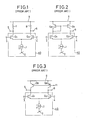
- Fig. 1 is a circuit diagram of a differential amplifier according to the first prior art.
- Fig. 2 is a circuit diagram of a differential amplifier according to the second prior art.
- Fig. 3, 4(A) and 4(B) are circuit diagrams of differential amplifiers according to the third prior art.
- Fig. 5, is a circuit diagram of a differential amplifier according to the fourth prior art.
- Fig. 6(A) and 6(B) are equivalent circuit diagrams for differential and common mode components, respectively, of the differential amplifier of Fig. 5.
- Fig. 7, 8 and 9 are circuit diagrams for explaining one embodiment of a differential amplifier according to the fourth prior art.
- Fig. 10 is a circuit diagram of the first embodiment of a differential amplifier according to the present invention.
- Fig. 11(A), (B), (C), (D) and (E) are diagrams of possible circuit elements to be incorporated in the differential amplifier of Fig. 10.
- Fig. 12 is a circuit diagram of the second embodiment of a differential amplifier according to the present invention.
- Fig. 13 is a graph showing the improvement of the dynamic range by the differential amplifier of Fig. 12.
- Fig. 14 is a circuit diagram of the third embodiment of a differential amplifier according to the present invention.
- Fig. 15 is a circuit diagram of the fourth embodiment of a differential amplifier according to the present invention.
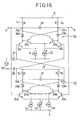
- Fig. 16 is a circuit diagram of the fifth embodiment of a differential amplifier according to the present invention.
- Fig. 17 is a circuit diagram of the sixth embodiment of a differential amplifier according to the present invention.
- Fig. 18 is a circuit diagram of the seventh embodiment of a differential amplifier according to the present invention.
- Fig. 19 is a circuit diagram of the eighth embodiment of a differential amplifier according to the present invention.
- Fig. 20(A) and (B) are partial circuit diagrams of possible variations of the differential amplifier according to the present invention.
- Fig. 21 is a circuit diagram of one application of a differential amplifier according to the present invention.
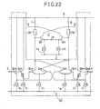
- Fig. 22 is a circuit diagram of another application of a differential amplifier according to the present invention.
- The various preferred embodiments of the present invention will now be explained. In the following description, as certain portions of the embodiments of the present invention overlap with those already explained in the description of the prior art, such parts are given the same symbols in the figures and their explanation will be omitted.
- Referring now to Fig. 10, there is shown the first embodiment of a differential amplifier according to the present invention. This differential amplifier incorporates, in addition to the differential amplifier of Fig. 9, two
level shift circuits level shift circuit 28 being connected between the base of the transistors Q₇ and the collector of the transistor Q₈, and thelevel shift circuit 29 being connected between the base of the transistors Q₈ and the collector of the transistor Q₇. Also in Fig. 10, the superfluouscurrent sources level shift circuits level shift circuits level shift circuits - The
level shift circuits - Referring now to Fig. 12, there is shown the second embodiment of a differential amplifier according to the present invention. In this embodiment the
level shift circuits input terminals output terminals curve 100 indicates the input-output characteristic of the differential amplifier of Fig. 9 which has no level shift circuit, and acurve 101 indicates the input-output characteristic of the differential amplifier of Fig. 12 which includes thelevel shift circuits - Moreover, due to the effect of the negative resistance produced by the positively feedbacked
differential amplifier 17, the output impedance of this differential amplifier can be quite large, although in practice contributions from the transistors of the positively feedbackeddifferential amplifier 17 lessen it to some extent. It is to be noted, however, that because of the variations in output resistance of the manufactured transistors, an attempt to make the magnitudes of the negative resistance by the positively feedbackeddifferential amplifier 17 and the net resistance of theload resistors - Referring now to Fig. 14, there is shown the third embodiment of a differential amplifier according to the present invention. In this embodiment the
level shift circuits current source 1 of Fig. 10 is replaced by a variable current source lb which can generate currents up to 2IQ and acapacitor 31 of capacitance C connected between thefirst terminals input terminals output terminals
gm = IQ/Vt (1)
where Vt = kT/q, k is the Boltzmann constant, T is the absolute temperature, and q is the charge of an electron, so that the output voltage Vout in terms of the input voltage Vin is given by:
Vout = gm · Vin / sC
=· · Vin (2) where s is a variable of the Laplace transform. This result can be considered as an integration of Vin. Now, since the time constant of this integrator is equal to C(Vt/IQ), by the variation of the currents from the variable
current source 1b it can function as an integrator with a variable time constant particularly suitable for an integrated active filter. Furthermore, in this embodiment, the capacitance of the integratingcapacitor 31 can be reduced compared with the prior art case such as one shown in Fig. 4(B), where twocapacitors capacitor 31 of this embodiment in order to obtain the same time constant. This aspect of the present embodiment can contribute to the reduction of the device size. - Referring now to Fig. 15, there is shown the fourth embodiment of a differential amplifier according to the present invention. In this embodiment the level shift circuits are diodes as in the previous embodiment, but the
terminal resistance 18 and thecapacitor 31 are removed and thecurrent source current source 32 connected to the emitters of the transistors Q₇ and Q₈ while the variablecurrent source 1b is replaced by the constantcurrent source 1 connected to the emitters of the transistors Q₁ and Q₂. For this differential amplifier, the input impedance of the positively feedbackeddifferential amplifier 17 seen from theoutput terminals differential amplifier 17. Namely, when the variablecurrent source 32 produces current I, the transconductance of each of the transistors Q₁ and Q₈ is equal to I/2Vt, and the input impedance r which is the same as a negative of a sum of the inverse of the transconductances is given by:
current source 32. Thus the load for the transistors Q₁ and Q₂ is given by:
- Referring now to Fig. 16, there is shown the fifth embodiment of a differential amplifier according to the present invention. In this embodiment, a
first integrator 33 identical to that of Fig. 14 is combined with asecond integrator 34 made by the amplifier of Fig. 15 equipped with aload capacitor 35 such that the bases of the transistor Q1b, Q2b, Q1c, Q2c are connected to theterminals capacitors terminals current source 32. - Referring now to Fig. 17, there is shown the sixth embodiment of a differential amplifier according to the present invention. In this embodiment the transistors Q₁, Q₂, Q₇, Q₈ of Fig. 10 are replaced by the GaAs MESFETs (Metal Semiconductor Field Effected Transistors) X₁, X₂, X₇, X₈ Now, GaAs MESFET in practice is predominantly n-channel type because p-channel type is considerably slow in response. Since this differential amplifier of the present embodiment can be constructed only by n-channel type GaAs MESFETs, it can contribute to flexibility in circuit designing and reduction in device size. It is to be noted that the similar situation exists for the GaAs heterojunction bipolar transistor whose pnp-type is considerably slow in response compared with npn-type and is also very hard to manufacture.
- Referring now to Fig. 18, there is shown the seventh embodiment of a differential amplifier according to the present invention. In this embodiment, GaAs MESFETs X₁, X₂, X₇, X₈ of the previous embodiment are replaced by Si MOSFETs (Metal Oxide Semiconductor Field Effect Transistors) Y₁, Y₂, Y₇, Y₈. Here again, p-channel type is considerably slow in response compared with n-channel type. Although in this case of Si MOSFET, p-channel type is also available and can be incorporated, this differential amplifier of the present embodiment which can be constructed only by n-channel type Si MOSFETs obviously can be faster in response and thus be considered superior than any amplifier involving p-channel type Si MOSFETs.
- Referring now to Fig. 19, there is shown the eighth embodiment of a differential amplifier according to the present invention. In this embodiment, Si MOSFETs Y₁, Y₂, Y₇, Y₈ of the previous embodiment are replaced by JFETs (Junction Field Effect Transistors) Z₁, Z₂, Z₇, Z₈. Here again, p-channel type is considerably slow in response compared with n-channel type. Although in this case of JFET as in the case of MOSFET, p-channel type is also available and can be incorporated, this differential amplifier of the present embodiment which can be constructed only by n-channel type JFETs obviously can be faster in response and thus be considered superior than any amplifier involving p-channel type JFETs.
- It can be easily understood that although the transistors Q₁ and Q₂ in the above embodiments formed an emitter-coupled pair in which their emitters are connected with each other directly, this configuration can be replaced by the so called emitter degeneration type such as those shown in Fig. 20(A) and (B). Though with such a replacement the amplification lowers, the linearity can be improved by means of the emitter degeneration so that it is possible to enhance the dynamic range further in the differential amplifier of the present invention. Similarly, although the transistors Q₇ and Q₈ in the above embodiments had the configuration similar to that shown in Fig. 20(A), it can be replaced by the configuration similar to that shown in Fig. 20(B) with the same effect.
- Similar improvement of the linearity as achieved by incorporating the emitter degeneration in the differential amplifier of the present invention above can be realized by the configurations shown in Figs. 21 and 22.
- In Fig. 21, the
differential amplification portion 40 of the differential amplifier of Fig. 10 is replaced by the linear differential amplifier proposed by J.C.Schmoock in "An Input Stage Transconductance Reduction Technique for High-Slew Rate Operational Amplifiers" IEEE Journal of Solid State Circuits, vol. SC-10, no.6, pp.407-411, December 1975. In this differential amplifier, the transistors Q1a and Q2b have the emitter areas four times as large as that of the transistors Q1b and Q2a and the constantcurrent sources - In Fig. 22, the
differential amplification portion 40 of the differential amplifier of Fig. 21 is modified so that the differential amplifier can operate faster. Namely, in this differential amplifier the transistors Q11a, Q2a, Q1b, and Q11b have the same emitter areas, but they are accompanied by the emitter followers formed by the transistors Q9a, Q9b, Q10a, and Q10b, and their emittercurrent sources - It can also easily be understood that, if only the pnp-type transistors or the p-channel type MOSFETs are required to be present in the device, it can easily be obtained by reversing the direction of the currents although obviously such a circuit is going to be very slow in response and will possess an inferior frequency characteristic.
- Moreover, many modifications and variations of these embodiments may be made without departing from the novel and advantageous features of the present invention. Accordingly, all such modifications and variations are intended to be included within the scope of the appended claims.
Claims (19)
1. A differential amplifier, comprising:
input terminals(3,4);
output terminals(5,6);
load resistor means(7,8) connected to the output terminals(5,6) for generating output voltages;
a pair of transistors(Q₁,Q₂), whose emitters are connected with each other, whose collectors are connected to the output terminals(5,6), and whose bases are coupled to the input terminals(3,4); and
current source means(1) connected to the emitters of the transistors for providing the emitter currents, characterized by comprising:
means(17) for producing negative resistance including level shift circuit means(28,29) for producing additional voltages, the means(17) being connected to the output terminal(3,4).
2. The amplifier of claim 1, wherein the means(17) for producing negative resistance include:
a second pair of transistors(Q₇,Q₈), whose emitters are connected with each other, each of whose collectors is connected to the base of the other transistor of the second pair(Q₇,Q₈) as well as to the output terminals(5,6);
second current source means(24,25) connected to the emitters of the second pair of transistors(Q₇,Q₈) for providing the emitter currents to the second pair of transistors(Q₇,Q₈);
a terminal resistor(18) connected between the emitters of the transistors of the second pair(Q₇,Q₈); and
the level shift circuit means(28,29) for producing additional voltages connected between the base of each transistor of the second pair(Q₇,Q₈) and the output terminals(5,6).
3. The amplifier of claim 1, wherein the level shift circuit means(28,29) comprises a battery.
4. The amplifier of claim 1, wherein the level shift circuit means(28,29) comprises at least one diode.
5. The amplifier of claim 1, wherein the level shift circuit means(28,29) comprises at least one transistor with its base connected to its collector.
6. The amplifier of claim 1, wherein the level shift circuit means(28,29) comprises a transistor with its base-emitter voltage amplified.
7. The amplifier of claim 1, wherein the level shift circuit means(28,29) comprises a resistor.
8. The amplifier of claim 2, further comprising capacitor means(31) connected to the output terminals(5,6) for accumulating charges, and wherein the current source means(1) is a variable current source.
9. The amplifier of claim 2, wherein the second current source means(24,25) is a variable current source, and wherein the resistance of the terminal resistor(18) is small.
10. The amplifier of claim 8, further comprising:
a second differential amplifier(34), comprising:
second input terminals;
second output terminals;
second load resistor means(7c,8c) connected to the second output terminals for generating output voltage;
second means for producing negative resistance connected to the second output terminals and including:
a third pair of transistors(Q1c,Q2c), whose emitters are connected with each other,each of whose collectors is connected to the base of the other transistor of the third pair(Q1c,Q2c) as well as to the second output terminals;
second variable current source means(32) connected to the emitters of the third pair of transistors(Q1c,Q2c) for providing the emitter currents to the third pair of transistors(Q1c,Q2c);
second level shift means(28c,29c) connected between the base of each transistor of the third pair(Q1c,Q2c) and the second output terminals for producing additional voltages;
second capacitor means(35) connected to the second output terminals for accumulating charges;
a fourth pair of transistors(Q7c,Q8c), whose emitters are connected with each other, whose collectors are connected to the second output terminals, and whose bases are coupled to the second input terminals;
constant current source means(1c) connected to the emitters of the fourth pair of transistors(Q7c,Q8c) for providing the emitter currents, the output terminals being connected to the second input terminals, the input terminals being connected to the second output terminals in reverse direction to the connection between the output terminals and the second input terminals;
third output terminals connected to the input terminals; and
third input terminals connected to the output terminals.
11. The amplifier of claim 1, wherein the transistors(Q₁,Q₂) are heterojunction bipolar transistors.
12. The amplifier of claim 1, wherein the transistors(Q₁,Q₂) are MESFETs(X₁,X₂).
13. The amplifier of claim 1, wherein the transistors(Q₁,Q₂) are MOSFETs(Y₁,Y₂).
14. The amplifier of claim 1, wherein the transistors(Q₁,Q₂) are JFETs(Z₁,Z₂).
15. The amplifier of claim 2, wherein the transistors of the second pair(Q₇,Q₈) are heterojunction bipolar transistors.
16. The amplifier of claim 2, wherein the transistors of the second pair(Q₇,Q₈) are MESFETs(X₇,X₈).
17. The amplifier of claim 2, wherein the transistors of the second pair(Q₇,Q₈) are MOSFETs(Y₇,Y₈).
18. The amplifier of claim 2, wherein the transistors of the second pair(Q₇,Q₈) are JFETs(Z₇,Z₈).
19. The amplifier of claim 1, further comprising an emitter degeneration resistor(39) between the emitters of the pair of transistors(Q₁,Q₂).
Applications Claiming Priority (2)
| Application Number | Priority Date | Filing Date | Title |
|---|---|---|---|
| JP62254785A JP2766264B2 (en) | 1987-10-12 | 1987-10-12 | Differential amplifier circuit |
| JP254785/87 | 1987-10-12 |
Publications (2)
| Publication Number | Publication Date |
|---|---|
| EP0312017A2 true EP0312017A2 (en) | 1989-04-19 |
| EP0312017A3 EP0312017A3 (en) | 1990-03-07 |
Family
ID=17269848
Family Applications (1)
| Application Number | Title | Priority Date | Filing Date |
|---|---|---|---|
| EP88116944A Withdrawn EP0312017A3 (en) | 1987-10-12 | 1988-10-12 | Differential amplifier |
Country Status (3)
| Country | Link |
|---|---|
| US (1) | US4904952A (en) |
| EP (1) | EP0312017A3 (en) |
| JP (1) | JP2766264B2 (en) |
Cited By (10)
| Publication number | Priority date | Publication date | Assignee | Title |
|---|---|---|---|---|
| EP0352790A2 (en) * | 1988-07-28 | 1990-01-31 | Kabushiki Kaisha Toshiba | Integrator and active filter including integrator with simple phase compensation |
| EP0400650A2 (en) * | 1989-05-31 | 1990-12-05 | Kabushiki Kaisha Toshiba | Linearized differential amplifier |
| EP0454982A1 (en) * | 1990-04-30 | 1991-11-06 | International Business Machines Corporation | Differential receiver |
| FR2741759A1 (en) * | 1995-11-29 | 1997-05-30 | Philips Electronics Nv | WIDE VOLTAGE AMPLIFIER RANGE OF VARIATION |
| EP0777322A1 (en) * | 1995-11-29 | 1997-06-04 | Philips Composants Et Semiconducteurs | Voltage amplifier with wide dynamic range and A/D converter using such amplifier |
| EP0863609A2 (en) * | 1997-03-05 | 1998-09-09 | Sony Corporation | Amplifier circuits |
| EP0884837A2 (en) * | 1997-06-14 | 1998-12-16 | Philips Patentverwaltung GmbH | Circuitry comprising a differential amplifying stage |
| WO2002056458A2 (en) * | 2001-01-10 | 2002-07-18 | Koninklijke Philips Electronics N.V. | A fully differential, variable-gain amplifier and a multidimensional amplifier arrangement |
| EP1603243A1 (en) * | 2004-05-31 | 2005-12-07 | STMicroelectronics S.r.l. | Prescaling stage for high frequency applications |
| IT201800005277A1 (en) * | 2018-05-11 | 2019-11-11 | System of amplification and transduction of a signal, in particular an electrical signal supplied to loudspeakers |
Families Citing this family (37)
| Publication number | Priority date | Publication date | Assignee | Title |
|---|---|---|---|---|
| US5754076A (en) * | 1993-12-13 | 1998-05-19 | Nec Corporation | Differential circuit having a variable current circuit for producing an exponential or a square transfer characteristic |
| US5089789A (en) * | 1990-05-16 | 1992-02-18 | Texas Instruments Incorporated | Differential amplifier |
| JPH04211508A (en) * | 1990-06-15 | 1992-08-03 | Toshiba Corp | Integrating circuit |
| US5053718A (en) * | 1990-07-03 | 1991-10-01 | Burr-Brown Corporation | Feedback control reducing signal distortion produced by differential amplifier stage |
| US5101126A (en) * | 1990-10-15 | 1992-03-31 | Analog Devices, Inc. | Wide dynamic range transconductance stage |
| GB9424878D0 (en) * | 1994-12-09 | 1995-02-08 | Plessey Semiconductors Ltd | Amplifier circuit arrangements |
| US5596299A (en) * | 1995-05-30 | 1997-01-21 | Philips Electronics North America Corporation | IF amplifier/limiter with positive feedback |
| US5587689A (en) * | 1995-09-28 | 1996-12-24 | Analog Devices, Inc. | Voltage controlled amplifier with a negative resistance circuit for reducing non-linearity distortion |
| US5821809A (en) * | 1996-05-23 | 1998-10-13 | International Business Machines Corporation | CMOS high-speed differential to single-ended converter circuit |
| JPH1056336A (en) * | 1996-08-09 | 1998-02-24 | Mitsubishi Electric Corp | Mixer circuit |
| JP2002330038A (en) * | 1997-01-16 | 2002-11-15 | Sony Corp | Common-emitter differential transistor circuit |
| JP3097598B2 (en) * | 1997-04-25 | 2000-10-10 | 日本電気株式会社 | Differential amplifier circuit |
| JPH11103237A (en) * | 1997-09-29 | 1999-04-13 | Sony Corp | High impedance circuit |
| FR2785107A1 (en) * | 1998-10-27 | 2000-04-28 | Koninkl Philips Electronics Nv | LOW INPUTANCE CURRENT AMPLIFIER |
| US5994959A (en) * | 1998-12-18 | 1999-11-30 | Maxim Integrated Products, Inc. | Linearized amplifier core |
| US7038542B2 (en) * | 2003-10-22 | 2006-05-02 | Kabushiki Kaisha Toshiba | Variable gain amplifier |
| US20050135468A1 (en) * | 2003-12-19 | 2005-06-23 | Bhushan Asuri | Feed forward filter |
| US20050134350A1 (en) * | 2003-12-19 | 2005-06-23 | Huang Lawrence L. | Analog delay circuit |
| US7561619B2 (en) * | 2003-12-19 | 2009-07-14 | Intel Corporation | Feedback filter |
| US20060280239A1 (en) * | 2005-06-09 | 2006-12-14 | Joachim Moll | Signal shaping circuit |
| CN100399224C (en) * | 2005-06-21 | 2008-07-02 | 电子科技大学 | Current source with very high output impedance |
| US7414456B2 (en) * | 2006-08-17 | 2008-08-19 | Analog Devices, Inc. | Constant ratio current source |
| US8319562B2 (en) * | 2009-08-26 | 2012-11-27 | Qualcomm Incorporated | System and method for amplifying a signal using multiple amplification stages sharing a common bias current |
| WO2012139079A2 (en) | 2011-04-07 | 2012-10-11 | Colburn Joseph S | Tunable impedance surfaces |
| EP2695296B1 (en) * | 2011-04-07 | 2020-07-15 | HRL Laboratories, LLC | Non-foster circuit |
| US9407239B2 (en) | 2011-07-06 | 2016-08-02 | Hrl Laboratories, Llc | Wide bandwidth automatic tuning circuit |
| US8878636B2 (en) * | 2011-08-09 | 2014-11-04 | Analog Devices, Inc. | Techniques for developing a negative impedance |
| US10103445B1 (en) | 2012-06-05 | 2018-10-16 | Hrl Laboratories, Llc | Cavity-backed slot antenna with an active artificial magnetic conductor |
| JP6102198B2 (en) * | 2012-11-14 | 2017-03-29 | 富士通株式会社 | Amplifier circuit |
| US9520849B2 (en) * | 2012-11-16 | 2016-12-13 | Texas Instruments Incorporated | Rail-to-rail constant transconductance differential input stage |
| US9705201B2 (en) | 2014-02-24 | 2017-07-11 | Hrl Laboratories, Llc | Cavity-backed artificial magnetic conductor |
| US20150372844A1 (en) * | 2014-06-18 | 2015-12-24 | Texas Instruments Incorporated | Wideband Parasitic Capacitance Cancellation for High Speed Switches in Serial Communication |
| US9425769B1 (en) | 2014-07-18 | 2016-08-23 | Hrl Laboratories, Llc | Optically powered and controlled non-foster circuit |
| US10193233B1 (en) | 2014-09-17 | 2019-01-29 | Hrl Laboratories, Llc | Linearly polarized active artificial magnetic conductor |
| FR3044845B1 (en) * | 2015-12-02 | 2019-03-15 | Commissariat A L'energie Atomique Et Aux Energies Alternatives | NEGATIVE IMPEDANCE CIRCUIT |
| US11024952B1 (en) | 2019-01-25 | 2021-06-01 | Hrl Laboratories, Llc | Broadband dual polarization active artificial magnetic conductor |
| CN110504933A (en) * | 2019-08-07 | 2019-11-26 | 宁波大学 | A kind of highly linear variable gain amplifier |
Citations (3)
| Publication number | Priority date | Publication date | Assignee | Title |
|---|---|---|---|---|
| GB2057800A (en) * | 1979-09-17 | 1981-04-01 | Tektronix Inc | Wideband differential amplifier |
| US4322688A (en) * | 1979-10-11 | 1982-03-30 | Tektronix, Inc. | Cascode feed-forward amplifier |
| EP0171095A1 (en) * | 1984-06-12 | 1986-02-12 | Koninklijke Philips Electronics N.V. | Level-shifting circuit |
Family Cites Families (5)
| Publication number | Priority date | Publication date | Assignee | Title |
|---|---|---|---|---|
| US4468629A (en) * | 1982-05-27 | 1984-08-28 | Trw Inc. | NPN Operational amplifier |
| JPS58213414A (en) * | 1982-06-04 | 1983-12-12 | Nippon Telegr & Teleph Corp <Ntt> | Semiconductor device for vapor growth |
| US4468628A (en) * | 1983-01-17 | 1984-08-28 | Tektronix, Inc. | Differential amplifier with high common-mode rejection |
| DE3574543D1 (en) * | 1984-05-16 | 1990-01-04 | Siemens Ag | BIPOLAR AMPLIFIER CIRCUIT. |
| NL8501882A (en) * | 1985-07-01 | 1987-02-02 | Philips Nv | SIGNAL VOLTAGE CURRENT CONVERTER. |
-
1987
- 1987-10-12 JP JP62254785A patent/JP2766264B2/en not_active Expired - Lifetime
-
1988
- 1988-10-06 US US07/254,242 patent/US4904952A/en not_active Expired - Lifetime
- 1988-10-12 EP EP88116944A patent/EP0312017A3/en not_active Withdrawn
Patent Citations (3)
| Publication number | Priority date | Publication date | Assignee | Title |
|---|---|---|---|---|
| GB2057800A (en) * | 1979-09-17 | 1981-04-01 | Tektronix Inc | Wideband differential amplifier |
| US4322688A (en) * | 1979-10-11 | 1982-03-30 | Tektronix, Inc. | Cascode feed-forward amplifier |
| EP0171095A1 (en) * | 1984-06-12 | 1986-02-12 | Koninklijke Philips Electronics N.V. | Level-shifting circuit |
Non-Patent Citations (1)
| Title |
|---|
| JOURNAL OF THE AUDIO ENGINEERING SOCIETY, vol. 29, no. 7/8, July/August 1981, pages 503-510, Audio Engineering Society, Inc. New York, US; M.J. HAWKSFORD: "Distortion correction circuits for audio amplifiers" * |
Cited By (18)
| Publication number | Priority date | Publication date | Assignee | Title |
|---|---|---|---|---|
| EP0352790A2 (en) * | 1988-07-28 | 1990-01-31 | Kabushiki Kaisha Toshiba | Integrator and active filter including integrator with simple phase compensation |
| EP0352790A3 (en) * | 1988-07-28 | 1991-07-10 | Kabushiki Kaisha Toshiba | Integrator and active filter including integrator with simple phase compensation |
| US5081423A (en) * | 1988-07-28 | 1992-01-14 | Kabushiki Kaisha Toshiba | Integrator and active filter including integrator with simple phase compensation |
| EP0400650A2 (en) * | 1989-05-31 | 1990-12-05 | Kabushiki Kaisha Toshiba | Linearized differential amplifier |
| EP0400650B1 (en) * | 1989-05-31 | 1996-10-09 | Kabushiki Kaisha Toshiba | Linearized differential amplifier |
| EP0454982A1 (en) * | 1990-04-30 | 1991-11-06 | International Business Machines Corporation | Differential receiver |
| US5774086A (en) * | 1995-11-29 | 1998-06-30 | U.S. Philips Corporation | Voltage amplifier having a large range of variations, and A/D converter comprising such an amplifier |
| EP0777322A1 (en) * | 1995-11-29 | 1997-06-04 | Philips Composants Et Semiconducteurs | Voltage amplifier with wide dynamic range and A/D converter using such amplifier |
| FR2741759A1 (en) * | 1995-11-29 | 1997-05-30 | Philips Electronics Nv | WIDE VOLTAGE AMPLIFIER RANGE OF VARIATION |
| EP0777321A3 (en) * | 1995-11-29 | 1999-09-22 | Philips Composants Et Semiconducteurs | Amplification of a voltage having wide variation and A-D converter comprising such an amplifier |
| EP0863609A2 (en) * | 1997-03-05 | 1998-09-09 | Sony Corporation | Amplifier circuits |
| EP0863609A3 (en) * | 1997-03-05 | 2000-02-16 | Sony Corporation | Amplifier circuits |
| EP0884837A2 (en) * | 1997-06-14 | 1998-12-16 | Philips Patentverwaltung GmbH | Circuitry comprising a differential amplifying stage |
| EP0884837A3 (en) * | 1997-06-14 | 2001-01-17 | Philips Patentverwaltung GmbH | Circuitry comprising a differential amplifying stage |
| WO2002056458A2 (en) * | 2001-01-10 | 2002-07-18 | Koninklijke Philips Electronics N.V. | A fully differential, variable-gain amplifier and a multidimensional amplifier arrangement |
| WO2002056458A3 (en) * | 2001-01-10 | 2003-03-13 | Koninkl Philips Electronics Nv | A fully differential, variable-gain amplifier and a multidimensional amplifier arrangement |
| EP1603243A1 (en) * | 2004-05-31 | 2005-12-07 | STMicroelectronics S.r.l. | Prescaling stage for high frequency applications |
| IT201800005277A1 (en) * | 2018-05-11 | 2019-11-11 | System of amplification and transduction of a signal, in particular an electrical signal supplied to loudspeakers |
Also Published As
| Publication number | Publication date |
|---|---|
| EP0312017A3 (en) | 1990-03-07 |
| US4904952A (en) | 1990-02-27 |
| JP2766264B2 (en) | 1998-06-18 |
| JPH0198305A (en) | 1989-04-17 |
Similar Documents
| Publication | Publication Date | Title |
|---|---|---|
| EP0312017A2 (en) | Differential amplifier | |
| JP3333239B2 (en) | Variable gain circuit | |
| JP2603968B2 (en) | Linear differential amplifier circuit | |
| US4723110A (en) | Transconductance amplifier | |
| US5465072A (en) | Tunable operational transcondunctance amplifier having high linearity | |
| Mahattanakul et al. | Current-mode versus voltage-mode G/sub m/-C biquad filters: what the theory says | |
| US5345190A (en) | Modular low voltage filter with common mode feedback | |
| JP3390093B2 (en) | Differential amplifier | |
| US4629973A (en) | Current stabilizing circuit operable at low power supply voltages | |
| US5392002A (en) | Low voltage bipolar negative impedance converter | |
| JPH0834395B2 (en) | Amplifier circuit with switch | |
| JP2622321B2 (en) | High frequency cross junction folded cascode circuit | |
| US4686487A (en) | Current mirror amplifier | |
| US5053718A (en) | Feedback control reducing signal distortion produced by differential amplifier stage | |
| EP0475507B1 (en) | Amplifier arrangement | |
| JPS63136707A (en) | Filter circuit and filter device employing the same | |
| JPH0514119A (en) | Integration circuit | |
| US4757275A (en) | Wideband closed loop amplifier | |
| US4998074A (en) | Transistor circuit with base-current compensation | |
| JPH05299949A (en) | Feedback type differential amplifier circuit | |
| US6031424A (en) | Differential amplifier with improved voltage gain using operational amplifiers to eliminate diode voltage drops | |
| JPH07142941A (en) | Amplifier output stage | |
| US4267521A (en) | Compound transistor circuitry | |
| JP3833530B2 (en) | Differential amplifier | |
| US5859566A (en) | Electronic circuit comprising complementary transconductors for filters and oscillators |
Legal Events
| Date | Code | Title | Description |
|---|---|---|---|
| PUAI | Public reference made under article 153(3) epc to a published international application that has entered the european phase |
Free format text: ORIGINAL CODE: 0009012 |
|
| 17P | Request for examination filed |
Effective date: 19881012 |
|
| AK | Designated contracting states |
Kind code of ref document: A2 Designated state(s): DE FR |
|
| PUAL | Search report despatched |
Free format text: ORIGINAL CODE: 0009013 |
|
| AK | Designated contracting states |
Kind code of ref document: A3 Designated state(s): DE FR |
|
| 17Q | First examination report despatched |
Effective date: 19920508 |
|
| STAA | Information on the status of an ep patent application or granted ep patent |
Free format text: STATUS: THE APPLICATION IS DEEMED TO BE WITHDRAWN |
|
| 18D | Application deemed to be withdrawn |
Effective date: 19920919 |