EP0288075B1 - Sub-booster circuit for stepping up an output voltage of main booster circuit - Google Patents
Sub-booster circuit for stepping up an output voltage of main booster circuit Download PDFInfo
- Publication number
- EP0288075B1 EP0288075B1 EP88106492A EP88106492A EP0288075B1 EP 0288075 B1 EP0288075 B1 EP 0288075B1 EP 88106492 A EP88106492 A EP 88106492A EP 88106492 A EP88106492 A EP 88106492A EP 0288075 B1 EP0288075 B1 EP 0288075B1
- Authority
- EP
- European Patent Office
- Prior art keywords
- mos transistor
- booster circuit
- circuit
- sub
- voltage
- Prior art date
- Legal status (The legal status is an assumption and is not a legal conclusion. Google has not performed a legal analysis and makes no representation as to the accuracy of the status listed.)
- Expired - Lifetime
Links
Images

Classifications
-
- G—PHYSICS
- G11—INFORMATION STORAGE
- G11C—STATIC STORES
- G11C11/00—Digital stores characterised by the use of particular electric or magnetic storage elements; Storage elements therefor
- G11C11/21—Digital stores characterised by the use of particular electric or magnetic storage elements; Storage elements therefor using electric elements
- G11C11/34—Digital stores characterised by the use of particular electric or magnetic storage elements; Storage elements therefor using electric elements using semiconductor devices
- G11C11/40—Digital stores characterised by the use of particular electric or magnetic storage elements; Storage elements therefor using electric elements using semiconductor devices using transistors
-
- G—PHYSICS
- G11—INFORMATION STORAGE
- G11C—STATIC STORES
- G11C5/00—Details of stores covered by group G11C11/00
- G11C5/14—Power supply arrangements, e.g. power down, chip selection or deselection, layout of wirings or power grids, or multiple supply levels
- G11C5/145—Applications of charge pumps; Boosted voltage circuits; Clamp circuits therefor
-
- G—PHYSICS
- G11—INFORMATION STORAGE
- G11C—STATIC STORES
- G11C16/00—Erasable programmable read-only memories
- G11C16/02—Erasable programmable read-only memories electrically programmable
- G11C16/06—Auxiliary circuits, e.g. for writing into memory
- G11C16/30—Power supply circuits
-
- H—ELECTRICITY
- H03—ELECTRONIC CIRCUITRY
- H03K—PULSE TECHNIQUE
- H03K17/00—Electronic switching or gating, i.e. not by contact-making and –breaking
- H03K17/06—Modifications for ensuring a fully conducting state
-
- H—ELECTRICITY
- H03—ELECTRONIC CIRCUITRY
- H03K—PULSE TECHNIQUE
- H03K3/00—Circuits for generating electric pulses; Monostable, bistable or multistable circuits
- H03K3/02—Generators characterised by the type of circuit or by the means used for producing pulses
- H03K3/353—Generators characterised by the type of circuit or by the means used for producing pulses by the use, as active elements, of field-effect transistors with internal or external positive feedback
- H03K3/356—Bistable circuits
- H03K3/356008—Bistable circuits ensuring a predetermined initial state when the supply voltage has been applied; storing the actual state when the supply voltage fails
Definitions
- This invention relates to a MOS semiconductor integrated circuit, and more particularly to a sub-booster circuit for stepping up an output voltage of a main booster circuit which generates a voltage higher than a power source voltage.
- EPROM and EEPROM floating gate type nonvolatile semiconductor memories
- Data can be electrically written into the EPROM and erased by application of ultraviolet rays.
- EEPROM data can be written and erased electrically.
- This type of semiconductor memory includes, for example, a memory which utilizes the Fowler-Nordheim tunneling effect. In the memory utilizing the tunneling effect, electrons are injected into or discharged from the floating gate via the thin oxide film in the data write-in or erasing operation. In the data write-in or erasing operation, there is little current consumption.
- the data write-in or erasing operation can be effected by using an output voltage of a booster circuit provided in the memory instead of externally applying a high voltage required for the data write-in or erasing operation.
- the booster circuit has a low current supplying ability, it can be used without any serious problem.
- the circuit scale of the nonvolatile memory becomes large and the number of peripheral circuits (load circuits) to be supplied with a stepped-up voltage increases. Therefore, the load capacitance of the booster circuit increases, thereby making it necessary to take a long step-up time for raising an output voltage to a desired level.
- the load circuits to be supplied with an output voltage of the booster circuit are divided into a plurality of blocks and transfer gates are connected to input terminals of the respective blocks. The transfer gates are selectively activated by a control signal for selecting one of the blocks. An output voltage of the booster circuit is supplied to the load circuit block via the selected transfer gate. Thus, the load capacitance of the booster circuit is lowered, preventing the voltage step-up time from being increased.
- the output voltage of the sub-booster circuit is supplied to the transfer gates to selectively activate the transfer gate. Since the transfer gate is selectively activated by a high voltage (equal to or higher than the sum of an output voltage of the main booster circuit and the threshold voltage of the transfer gate) of the sub-booster circuit, a voltage supplied from the booster circuit to the load circuit block will not be lowered by the threshold voltage of the transfer gate. Therefore, the output voltage of the booster circuit is efficiently supplied to the selected load circuit block.
- the load capacitance of the main booster circuit can be lowered, thereby permitting a stepped-up voltage to be supplied to the load circuit in a brief time without lowering the output voltage of the main booster circuit.
- a high voltage used for writing or erasing data in a semiconductor memory can be generated in the semiconductor integrated circuit (such as a nonvolatile semiconductor memory).
- a MOS transistor is used in the input stage of the load circuit, and a stepped-up voltage is applied to the gate of the MOS transistor. Therefore, a voltage supplied to the internal circuit of the load circuit is lowered by the threshold voltage of the input stage MOS transistor. For this reason, it is preferable to further raise an output voltage of the main booster circuit by means of the sub-booster circuit and supply it to the gate of the input stage MOS transistor even when the load circuits are not divided into a plurality of blocks.
- the voltage step-up efficiency of the sub-booster circuit which is commonly used is not sufficiently high to further raise the output voltage of the main booster circuit, and therefore it is strongly required to develop the sub-booster circuit.
- US-A-4 511 811 discloses a charge pump for providing a programming voltage to the word lines in a semiconductor memory array.
- the charge pump configured as a combination of enhancement and native MOS transistors, prevents DC current from flowing from the source of the programming voltage to ground through unselected word lines, and thereby permits the design of semiconductor programmable memory arrays having on-chip voltage generation, allowing for design of semiconductor programmable memory arrays which operate from a single voltage power supply.
- the charge pump is connected, at one end thereof, to a high voltage source, and at the other end thereof to a word line. The output voltage of the charge pump supplied to the word line cannot exceed the output voltage of the high voltage source.
- An oscillator supplies pulses to the high voltage source and to a capacitive coupling device of the charge pump.
- the coupling device has its gate terminal connected to a node of the charge pump, and has its source and drain terminals together connected to the oscillator.
- An enhancement MOS device has its drain and gate terminals connected to the node and its source terminal connected to the word line, and this MOS device is turned OFF when that word line is not selected because the node is at zero volts.
- a native MOS transistor serving as a transfer device has its source terminal connected to the node, its gate terminal connected to the word line, and its drain terminal connected to the source terminal of an enhancement MOS device, the drain and gate terminals of which are together connected to the output of the high voltage source such that the latter MOS device acts like a diode providing a unidirectional current path from the high voltage source to the MOS transfer device.
- the MOS diode has a threshold voltage of 1.5 volts
- the MOS transfer device has a threshold voltage of either zero or 0.5 volts
- the enhancement MOS device which is connected between the coupling device and the word line has a threshold voltage of 1.0 volts.
- the word line will incrementally charge up to the voltage at the output of the high voltage source.
- An object of this invention is to provide a sub-booster circuit capable of raising an output voltage of a main booster circuit at a high efficiency.
- ON-resistances of the first and second switching circuits can be set to a small value and the second switching circuit can be kept in the off condition when the clock pulse falls. Therefore, a sub-booster circuit is provided in which reduction in the output voltage caused by the presence of the first and second switching circuits may be suppressed to a minimum and which is operated to raise a voltage at a high step-up efficiency and high reliability.
- Fig. 1 shows a sub-booster circuit according to one embodiment of this invention and the peripheral circuits thereof.
- Power source voltage Vcc (or externally supplied high voltage Vpp) is stepped up or boosted by means of main booster circuit 11.
- Stepped-up voltage Vpu which is obtained by raising power source voltage Vcc or high voltage Vpp by using main booster circuit 11 is supplied to sub-booster circuit 12 and object circuit 13 which is operated by the stepped-up voltage.
- Sub-booster circuit 12 includes N-channel MOS transistors Q1 and Q2 and MOS capacitor C1. The drain of MOS transistor Q1 is connected to the output terminal of main booster circuit 11, and the gate thereof is connected to the output terminal (node N1) of selection circuit 14.
- the input terminal of selection circuit 14 is connected to receive selection signals SS1 to SSn for selecting sub-booster circuit 12. Further, the output terminal of selection circuit 14 is connected to the input terminal of object circuit 13.
- the source of MOS transistor Q1 is connected to the drain and gate of MOS transistor Q2 and the source of MOS transistor Q2 is connected to node N1.
- a connection node (node N2) between the source of MOS transistor Q1 and the drain of MOS transistor Q2 is connected to a first electrode of MOS capacitor C1.
- a second electrode of MOS capacitor C1 is connected to the output terminal of clock generation circuit 15 so as to receive clock pulse ⁇ c.
- Object circuit 13 includes N-channel MOS transistor Q3.
- the drain of MOS transistor Q3 is connected to the output terminal of main booster circuit 11 and the gate thereof is connected to node N1. Further, the source of MOS transistor Q3 is connected to an internal circuit which is not shown.
- a parasitic capacitor such as a wiring capacitor and a gate capacitor is denoted by capacitor C2 which is grounded at one electrode.
- V1b denotes a potential at node N1 after the rise potential has been reached.
- potential V1a at node N1 rises by "(V ⁇ - V TH1 - V TH2 ) ⁇ C1/(C1 + C2)".
- V GS2 denotes a potential difference between the gate and source of MOS transistor Q2.
- a booster circuit having a high step-up efficiency can be obtained by satisfying the condition on the threshold voltage. Further, if condition (d) is satisfied, a booster circuit capable of supplying a high stepped-up voltage can be designed while the reduction of the output voltage due to the threshold voltage of MOS transistors Q1 and Q2 can be suppressed to a minimum. In the first embodiment, this is achieved by using an intrinsic MOS transistor having a threshold voltage of substantially 0 V as MOS transistor Q1 and using an enhancement type MOS transistor having a positive threshold voltage as MOS transistor Q2.
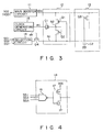
- Fig. 3 shows a sub-booster circuit according to a second embodiment of this invention and peripheral circuits thereof. Portions in Fig. 3 which correspond to those in Fig. 1 are denoted by the same reference numerals and the explanations thereof are therefore omitted.
- Depletion type N-channel MOS transistor Q4 having a gate grounded is connected between the output terminal of selection circuit 14 and node N1 of sub-booster circuit 12.
- sub-booster circuit 14 includes NAND gate (or NOR gate) 16 and CMOS inverter 17.
- Input terminals of NAND gate 16 are connected to receive selection signals SS1 to SSn (which can be replaced by address signals in the case of memory) which are used to select sub-booster circuit 12.
- an output potential of CMOS inverter 17 is set to a Vcc level (for example, 5 V), and when sub-booster circuit 12 is not selected, the output potential is set to 0 V.
- Vcc level for example, 5 V
- MOS capacitor C1 is formed to have the same structure as enhancement type MOS transistor Q2 so as to have threshold voltage V THC of 1 V, for example, MOS transistor Q1 is formed to have threshold voltage V TH1 of 0 V, and MOS transistor Q4 is formed in the same manner as a depletion type so as to have threshold voltage V TH4 of -3 V, for example.
- a sub-booster circuit which can step up an output voltage of a main booster circuit with a high step-up efficiency can be provided.
Description
- This invention relates to a MOS semiconductor integrated circuit, and more particularly to a sub-booster circuit for stepping up an output voltage of a main booster circuit which generates a voltage higher than a power source voltage.
- In recent years, floating gate type nonvolatile semiconductor memories called EPROM and EEPROM have rapidly spread. Data can be electrically written into the EPROM and erased by application of ultraviolet rays. In the EEPROM, data can be written and erased electrically. This type of semiconductor memory includes, for example, a memory which utilizes the Fowler-Nordheim tunneling effect. In the memory utilizing the tunneling effect, electrons are injected into or discharged from the floating gate via the thin oxide film in the data write-in or erasing operation. In the data write-in or erasing operation, there is little current consumption. Therefore, the data write-in or erasing operation can be effected by using an output voltage of a booster circuit provided in the memory instead of externally applying a high voltage required for the data write-in or erasing operation. Thus, even if the booster circuit has a low current supplying ability, it can be used without any serious problem.
- Recently, the circuit scale of the nonvolatile memory becomes large and the number of peripheral circuits (load circuits) to be supplied with a stepped-up voltage increases. Therefore, the load capacitance of the booster circuit increases, thereby making it necessary to take a long step-up time for raising an output voltage to a desired level. In the semiconductor integrated circuit, the load circuits to be supplied with an output voltage of the booster circuit are divided into a plurality of blocks and transfer gates are connected to input terminals of the respective blocks. The transfer gates are selectively activated by a control signal for selecting one of the blocks. An output voltage of the booster circuit is supplied to the load circuit block via the selected transfer gate. Thus, the load capacitance of the booster circuit is lowered, preventing the voltage step-up time from being increased.
- As described above, in the case where the load circuits are divided into a plurality of blocks, it is necessary to apply a voltage higher than an output voltage of the booster circuit to the gate of the transfer gate. In other words, it is necessary to set the control signal for controlling the transfer gate higher than the output voltage of the booster circuit. This is because the voltage supplied to the load circuit block is lowered by the threshold voltage of the transfer gate. For this reason, a sub-booster circuit is used in addition to a main booster circuit in order to further raise a voltage which has been stepped up by the main booster circuit. An output voltage of the sub-booster circuit is higher than the output voltage of the main booster circuit by more than the threshold voltage of the transfer gate. The output voltage of the sub-booster circuit is supplied to the transfer gates to selectively activate the transfer gate. Since the transfer gate is selectively activated by a high voltage (equal to or higher than the sum of an output voltage of the main booster circuit and the threshold voltage of the transfer gate) of the sub-booster circuit, a voltage supplied from the booster circuit to the load circuit block will not be lowered by the threshold voltage of the transfer gate. Therefore, the output voltage of the booster circuit is efficiently supplied to the selected load circuit block.
- With the use of the sub-booster circuit, the load capacitance of the main booster circuit can be lowered, thereby permitting a stepped-up voltage to be supplied to the load circuit in a brief time without lowering the output voltage of the main booster circuit. In this way, a high voltage used for writing or erasing data in a semiconductor memory can be generated in the semiconductor integrated circuit (such as a nonvolatile semiconductor memory).
- Further, in a MOS semiconductor integrated circuit, a MOS transistor is used in the input stage of the load circuit, and a stepped-up voltage is applied to the gate of the MOS transistor. Therefore, a voltage supplied to the internal circuit of the load circuit is lowered by the threshold voltage of the input stage MOS transistor. For this reason, it is preferable to further raise an output voltage of the main booster circuit by means of the sub-booster circuit and supply it to the gate of the input stage MOS transistor even when the load circuits are not divided into a plurality of blocks.
- For the reasons described above, it is required to use a highly efficient sub-booster circuit. However, the voltage step-up efficiency of the sub-booster circuit which is commonly used is not sufficiently high to further raise the output voltage of the main booster circuit, and therefore it is strongly required to develop the sub-booster circuit.
- US-A-4 511 811 discloses a charge pump for providing a programming voltage to the word lines in a semiconductor memory array. The charge pump, configured as a combination of enhancement and native MOS transistors, prevents DC current from flowing from the source of the programming voltage to ground through unselected word lines, and thereby permits the design of semiconductor programmable memory arrays having on-chip voltage generation, allowing for design of semiconductor programmable memory arrays which operate from a single voltage power supply. The charge pump is connected, at one end thereof, to a high voltage source, and at the other end thereof to a word line. The output voltage of the charge pump supplied to the word line cannot exceed the output voltage of the high voltage source.
- An oscillator supplies pulses to the high voltage source and to a capacitive coupling device of the charge pump. The coupling device has its gate terminal connected to a node of the charge pump, and has its source and drain terminals together connected to the oscillator. An enhancement MOS device has its drain and gate terminals connected to the node and its source terminal connected to the word line, and this MOS device is turned OFF when that word line is not selected because the node is at zero volts.
- A native MOS transistor serving as a transfer device has its source terminal connected to the node, its gate terminal connected to the word line, and its drain terminal connected to the source terminal of an enhancement MOS device, the drain and gate terminals of which are together connected to the output of the high voltage source such that the latter MOS device acts like a diode providing a unidirectional current path from the high voltage source to the MOS transfer device.
- The MOS diode has a threshold voltage of 1.5 volts, the MOS transfer device has a threshold voltage of either zero or 0.5 volts, and the enhancement MOS device which is connected between the coupling device and the word line has a threshold voltage of 1.0 volts.
- Eventually, after many cycles of the oscillator, the word line will incrementally charge up to the voltage at the output of the high voltage source.
- An object of this invention is to provide a sub-booster circuit capable of raising an output voltage of a main booster circuit at a high efficiency.
- The object is achievied by a sub-booster circuit according to either one of
independent claims 1, 8, and 13. - Preferred embodiments of the invention are indicated in the dependent claims.
- With this construction, ON-resistances of the first and second switching circuits can be set to a small value and the second switching circuit can be kept in the off condition when the clock pulse falls. Therefore, a sub-booster circuit is provided in which reduction in the output voltage caused by the presence of the first and second switching circuits may be suppressed to a minimum and which is operated to raise a voltage at a high step-up efficiency and high reliability.
- This invention can be more fully understood from the following detailed description when taken in conjunction with the accompanying drawings, in which:
- Fig. 1 is a circuit diagram showing a sub-booster circuit according to a first embodiment of this invention;
- Fig. 2 is a timing chart for illustrating the operation of a circuit shown in Fig. 1;
- Fig. 3 is a circuit diagram showing a sub-booster circuit according to a second embodiment of this invention; and
- Fig. 4 is a circuit diagram showing the construction of a selection circuit used in the circuit shown in Fig. 3.
- Fig. 1 shows a sub-booster circuit according to one embodiment of this invention and the peripheral circuits thereof. Power source voltage Vcc (or externally supplied high voltage Vpp) is stepped up or boosted by means of
main booster circuit 11. Stepped-up voltage Vpu which is obtained by raising power source voltage Vcc or high voltage Vpp by usingmain booster circuit 11 is supplied tosub-booster circuit 12 andobject circuit 13 which is operated by the stepped-up voltage.Sub-booster circuit 12 includes N-channel MOS transistors Q1 and Q2 and MOS capacitor C1. The drain of MOS transistor Q1 is connected to the output terminal ofmain booster circuit 11, and the gate thereof is connected to the output terminal (node N1) ofselection circuit 14. The input terminal ofselection circuit 14 is connected to receive selection signals SS1 to SSn for selectingsub-booster circuit 12. Further, the output terminal ofselection circuit 14 is connected to the input terminal ofobject circuit 13. The source of MOS transistor Q1 is connected to the drain and gate of MOS transistor Q2 and the source of MOS transistor Q2 is connected to node N1. A connection node (node N2) between the source of MOS transistor Q1 and the drain of MOS transistor Q2 is connected to a first electrode of MOS capacitor C1. A second electrode of MOS capacitor C1 is connected to the output terminal ofclock generation circuit 15 so as to receive clock pulse φc. -
Object circuit 13 includes N-channel MOS transistor Q3. The drain of MOS transistor Q3 is connected to the output terminal ofmain booster circuit 11 and the gate thereof is connected to node N1. Further, the source of MOS transistor Q3 is connected to an internal circuit which is not shown. In Fig. 1, a parasitic capacitor such as a wiring capacitor and a gate capacitor is denoted by capacitor C2 which is grounded at one electrode. - There will now be described the operation of the circuit with the construction described above with reference to the timing chart shown in Fig. 2. When an output signal on the output terminal (node N1) of
selection circuit 14 is set to a "1" level,sub-booster circuit 12 is selected, turning on MOS transistor Q1. As a result of this, potential V2a at node N2 is raised to a potential level which is lower than potential V1a at node N1 by threshold voltage VTH1 of N-channel MOS transistor Q1. An increase in potential V2a at node N2 renders MOS transistor Q1 nonconductive. Therefore, potential V2a at node N2 set at this time is given as follows:
- When potential V2a at node N2 is higher than threshold voltage VTHC of MOS capacitor C1, an inverted layer is formed under the gate of MOS capacitor C1, thus providing a coupling capacitor between the output terminal of
clock generation circuit 15 and node N2. Assume now that the input voltage level of the clock pulse is Vφ. Then, charge E1a expressed by the following equation (2) is stored in MOS capacitor C1:
- At this time, if the level of clock pulse φc is 0 V, charge E1a stored in MOS capacitor C1 is expressed as follows:

- In this case, if clock pulse φc with potential Vφ rises, a potential at node N2 is raised as a result of the capacitive coupling of capacitor C1. When the potential at node N2 becomes higher than a voltage obtained by adding threshold voltage VTH2 of N-channel MOS transistor Q2 to potential V1a at node N1, MOS transistor Q2 is turned on, causing the charge stored in capacitor C1 to be discharged to node N1 via MOS transistor Q2. Due to the discharge operation, the potential at node N1 rises. Since, in this case, MOS transistor Q2 is turned off again by a voltage obtained by adding threshold voltage VTH2 of MOS transistor Q2 to the potential at node N1, the potential at node N2 is kept at the potential level which is set up at this time. Therefore, potential V2b at node N2 is expressed as follows:

- V1b denotes a potential at node N1 after the rise potential has been reached.
- Therefore, charge E1b remaining in capacitor C1 can be expressed as follows:

- Further, initial charge E2a in load capacitor C2 at node N1 is expressed as follows:

Therefore, charge E2b stored in load capacitor C2 after the potential of the rise at node N1 has been reached can be expressed as follows:
- Since, at this time, total amount E of the charges stored in MOS capacitor C1 and load capacitor C2 is kept constant before and after the rise of clock pulse φc, it can be expressed as follows:

- Therefore, the following equation can be obtained:

- From equation (9), potential V1b at node N1 after the potential of the rise has been reached can be obtained as follows:

- Thus, potential V1a at node N1 rises by "(Vφ - VTH1 - VTH2) × C1/(C1 + C2)".
- Next, when clock pulse φc falls with potential -Vφ, the potential at node N2 starts to fall due to the capacitive coupling of MOS capacitor C1. However, when a potential at node N2 becomes lower than a voltage "V2c = V1b - VTH1", that is, a voltage which is lower than the gate voltage of MOS transistor Q1 or voltage V1b at node N1 by threshold voltage VTH1 of MOS transistor Q1, MOS transistor Q1 is turned on, thus restarting the charging of node N2. Therefore, the potential at node N2 rises to a potential of "V2c = V1b - VTH1" which may cause MOS transistor Q1 to be turned off. At this time, since gate voltage V2c of MOS transistor Q2 is lowered and MOS transistor Q2 is kept in the OFF condition, potential V1b at node N1 is kept constant.
- From the above description, it is clearly understood that potential V1 at node N1 is raised by an amount determined by "(Vφ - VTH1 - VTH2) × C1/(C1 + C2)" each time clock pulse φc rises. Therefore, in order to most efficiently operate
sub-booster circuit 12, care should be taken to satisfy the following conditions (a) to (d). - (a) The rise time of clock pulse φc should be set to be short.
- (b) The value of load capacitor C2 should be set to be small or coupling MOS capacitor C1 should be set to have a capacitance relatively larger than load capacitor C2 to make "C1/(C1 + C2)" as close to "1" as possible.
- (c) Input voltage level Vφ of clock pulse φc should be set to be high.
- (d) Threshold voltages VTH1 and VTH2 of MOS transistors Q1 and Q2 should be set to be low.
- However, in the MOS semiconductor integrated circuit, conditions (a) to (c) are determined by other factors and it is frequently impossible to satisfy these conditions. In order to satisfy condition (d), it is necessary to keep MOS transistor Q2 in the nonconductive state at the time clock pulse φc falls. The cutoff condition of MOS transistor Q2 can be expressed as follows:

- VGS2 denotes a potential difference between the gate and source of MOS transistor Q2.
- Since gate voltage VG of MOS transistor Q2 is "V1a - VTH1" and source voltage VS is "V1a", expression (11) can be rewritten as follows:

- Since VTH2 is positive, the following expression can be obtained;

- That is, a booster circuit having a high step-up efficiency can be obtained by satisfying the condition on the threshold voltage. Further, if condition (d) is satisfied, a booster circuit capable of supplying a high stepped-up voltage can be designed while the reduction of the output voltage due to the threshold voltage of MOS transistors Q1 and Q2 can be suppressed to a minimum. In the first embodiment, this is achieved by using an intrinsic MOS transistor having a threshold voltage of substantially 0 V as MOS transistor Q1 and using an enhancement type MOS transistor having a positive threshold voltage as MOS transistor Q2.
- Fig. 3 shows a sub-booster circuit according to a second embodiment of this invention and peripheral circuits thereof. Portions in Fig. 3 which correspond to those in Fig. 1 are denoted by the same reference numerals and the explanations thereof are therefore omitted. Depletion type N-channel MOS transistor Q4 having a gate grounded is connected between the output terminal of
selection circuit 14 and node N1 ofsub-booster circuit 12. For example, as shown in Fig. 4,sub-booster circuit 14 includes NAND gate (or NOR gate) 16 andCMOS inverter 17. Input terminals ofNAND gate 16 are connected to receive selection signals SS1 to SSn (which can be replaced by address signals in the case of memory) which are used to selectsub-booster circuit 12. Whensub-booster circuit 12 is selected, an output potential ofCMOS inverter 17 is set to a Vcc level (for example, 5 V), and whensub-booster circuit 12 is not selected, the output potential is set to 0 V. - MOS transistor Q4 is turned off when a potential at node N1 is stepped up, thus preventing the charge from being discharged from node N1. Further, when
sub-booster circuit 12 is selected, the potential at node N1 is set to a potential level of (-VTH4) obtained by subtracting threshold voltage VTH4 of MOS transistor Q4 from the gate voltage of MOS transistor Q4. When the potential at node N1 is set to (-VTH4), MOS transistor Q1 is turned on. Therefore, the potential appearing at node N2 at this time can be expressed as follows, based on equation (1) ("V2a = V1a - VTH1"):
- In order to attain the voltage step-up operation by means of
sub-booster circuit 12, it is necessary to set the potential at node N2 higher than threshold voltage VTHC of MOS capacitor C1 so as to form an inversion layer under the gate, thus forming a coupling capacitor. For this reason, it is required that potential V2a at node N2 be set higher than threshold voltage VTHC of MOS capacitor C1 at thetime circuit 12 is selected. Since V2a > VTH1, the following expression can be obtained:
- As is clearly seen from equation (15), if threshold voltage VTH1 of MOS transistor Q1 is set as low as possible, the condition set by expression (15) can be more easily satisfied, and consequently a large tolerance for variation in the threshold voltages occurring in the manufacturing process of MOS semiconductor integrated circuits can be attained.
- In the circuit of Fig. 3, MOS capacitor C1 is formed to have the same structure as enhancement type MOS transistor Q2 so as to have threshold voltage VTHC of 1 V, for example, MOS transistor Q1 is formed to have threshold voltage VTH1 of 0 V, and MOS transistor Q4 is formed in the same manner as a depletion type so as to have threshold voltage VTH4 of -3 V, for example.
- As described before, it is only required that the circuit of this invention satisfy the condition set by the expression "|VTH1| < VTH2". Therefore, when VTH2 is set to 1 V, the most efficient step-up operation can be attained by setting VTH1 to -0.9 V. Since the threshold voltage of MOS capacitor C1 is set to be equal to that of MOS transistor Q2, V2 is set to 0.9 V when
sub-booster circuit 12 is not selected, that is, at the time of V1 = 0 V. Therefore, in this case, no inversion layer is formed in MOS capacitor C1, and MOS capacitor can be substantially neglected. At this time, even if clock pulse φc has varied in level, the potential at node N2 will not change. - As described above, according to this invention, a sub-booster circuit which can step up an output voltage of a main booster circuit with a high step-up efficiency can be provided.
Claims (16)
- A sub-booster circuit for stepping up an output voltage (Vpu) of a main booster circuit (11) and supplying a stepped-up voltage to an object circuit (13), comprising:
first switching means (Q1) having a first end connected to receive the output voltage (Vpu) of said main booster circuit (11), a control terminal connected to an input terminal of said object circuit (13), and a second end; second switching means (Q2) having a first end and a control terminal connected to the second end of said first switching means (Q1), and a second end connected to the input terminal of said object circuit (13); and capacitive means (C1) having a first electrode connected to a connection node (N2) between said first and second switching means (Q1, Q2), and a second electrode connected to receive a clock pulse signal (φc); each of the first and second switching means (Q1, Q2) being turned on when a potential difference between its control terminal and its second end is higher than a predetermined voltage (VTH1 for Q1 and VTH2 for Q2); wherein a predetermined voltage (VTH2) for said second switching means (Q2) is set larger than the absolute value of the predetermined value (VTH1) of said first switching means (Q1); and wherein said capacitive means (C1) functions as a capacitor when a potential difference between its first and second electrodes is substantially equal to or higher than the potential difference which turns on said second switching means (Q2) and exhibits no capacitance property when the potential difference between its first and second electrodes is lower than the potential difference which turns on said second switching means (Q2). - A sub-booster circuit according to claim 1, characterized in that said first switching means includes an intrinsic type N-channel MOS transistor (Q1) and said second switching means includes an enhancement type N-channel MOS transistor (Q2).
- A sub-booster circuit according to claim 1, characterized in that said capacitive means includes a MOS capacitor (C1).
- A sub-booster circuit according to claim 1, characterized by further comprising a selection circuit (14) for determining whether or not an output voltage of said sub-booster circuit (12) has been supplied to said object circuit (13).
- A sub-booster circuit according to claim 4, characterized in that said selection circuit (14) includes a NAND gate (16) connected to receive selection signals (SSl to SSn), and a CMOS inverter (17) having an input terminal connected to receive an output signal of said NAND gate (16) and an output terminal connected to the input terminal of said object circuit (13).
- A sub-booster circuit according to claim 4, characterized in that said selection circuit (14) includes a NAND gate (16) connected to receive selection signals (SSl to SSn), a CMOS inverter (17) connected to receive an output signal of said NAND gate (16), and a depletion type MOS transistor (Q4) having a grounded gate and a current path connected between an output terminal of said CMOS inverter (17) and the input terminal of said object circuit (13).
- The combination of an object circuit (13) and a sub-booster circuit according to claim 1, wherein said object circuit (13) includes a MOS transistor (Q3) having a drain connected to the output terminal of said main booster circuit (11) and a gate connected to the second end of said second switching means (Q2).
- A sub-booster circuit for supplying a stepped-up voltage to an object circuit (13) comprising a first MOS transistor (Q1) having a drain connected to the output terminal of a main booster circuit (11), and a gate connected to an input terminal of said object cirucit (13); a second MOS transistor (Q2) having a drain and a gate connected to the source of said first MOS transistor (Q1) and a source connected to the input terminal of said object circuit (13); and a MOS capacitor (C1) having a first electrode connected to a connection node (N2) between said first and second MOS transistors (Q1 and Q2) and a second electrode connected to receive a clock pulse signal (φc), the threshold voltage of said second MOS transistor (Q2) being set larger than the absolute value of the threshold voltage of said first MOS transistor (Q1), wherein said MOS capacitor (C1) has substantially the same threshold voltage as said second MOS transistor (Q2), such that the output voltage (Vpu) of said main booster circuit (11) is stepped up.
- A sub-booster circuit according to claim 8, characterized in that said first MOS transistor (Q1) is an intrinsic type N-channel MOS transistor and said second MOS transistor (Q2) is an enhancement type N-channel MOS transistor.
- A sub-booster circuit according to claim 8, characterized by further comprising a selection circuit (14) for determining whether or not an output voltage of said sub-booster circuit (12) has been supplied to said object circuit (13).
- A sub-booster circuit according to claim 10, characterized in that said selection circuit (14) includes a NAND gate (16) connected to receive selection signals (SSl to SSn), and a CMOS inverter (17) having an input terminal connected to receive an output signal of said NAND gate (16) and an output terminal connected to the input terminal of said object circuit (13).
- A sub-booster circuit according to claim 10, characterized in that said selection circuit (14) includes a NAND gate (16) connected to receive selection signals (SSl to SSn), a CMOS inverter (17) connected to receive an output signal of said NAND gate (16), and a depletion type MOS transistor (Q4) having a grounded gate and a current path connected between an output terminal of said CMOS inverter (17) and the input terminal of said object circuit (13).
- A sub-booster circuit for stepping up an output voltage (Vpu) or a main booster circuit (11) and supplying a steppe-up voltage to an object circuit (13) which is selected by a selection circuit (14), comprising :
a first MOS transistor (Q1) having a drain connected to the output terminal of said main booster circuit (11), and a gate connected to an input terminal of said object circuit (13); a second MOS transistor (Q2) having a drain an a gate connected to the source of said first MOS transistor (Q1) and a source connected to the input terminal of said object circuit (13); a MOS capacitor (C1) having a first electrode connected to a connection node (N2) between said first and second MOS transistors to receive a clock pulse signal (φc); and a third MOS transistor (Q4) of a depletion type having a drain connected to the input terminal of said object circuit (13), a source connected to the output terminal of said selection circuit (14) and a grounded gate; wherein a threshold voltage of said second MOS transistor (Q2) is larger than the absolute value of a threshold voltage of said first MOS transistor (Q1), and said MOS capacitor (C1) has substantially the same threshold voltage as said second MOS transistor (Q2). - A sub-booster circuit according to claim 13, characterized in that said first MOS transistor (Q1) is an intrinsic type N-channel MOS transistor and said second MOS transistor (Q2) is an enhancement type N-channel MOS transistor.
- A sub-booster circuit according to claim 13, characterized in that said selection circuit (14) includes a NAND gate (16) connected to receive the selection signals, and a CMOS inverter (17) having an input terminal connected to receive an output signal of said NAND gate (16) and an output terminal connected to the input terminal of said object circuit (13).
- The combination of an object circuit (13) and a sub-booster circuit according to claim 13, wherein that said object circuit (13) includes a MOS transistor (Q3) having a drain connected to the output terminal of said main booster circuit (11) and a gate connected to the source of said second MOS transistor (Q2).
Applications Claiming Priority (2)
| Application Number | Priority Date | Filing Date | Title |
|---|---|---|---|
| JP10141987A JPH0748310B2 (en) | 1987-04-24 | 1987-04-24 | Semiconductor integrated circuit |
| JP101419/87 | 1987-04-24 |
Publications (3)
| Publication Number | Publication Date |
|---|---|
| EP0288075A2 EP0288075A2 (en) | 1988-10-26 |
| EP0288075A3 EP0288075A3 (en) | 1990-10-17 |
| EP0288075B1 true EP0288075B1 (en) | 1995-02-15 |
Family
ID=14300189
Family Applications (1)
| Application Number | Title | Priority Date | Filing Date |
|---|---|---|---|
| EP88106492A Expired - Lifetime EP0288075B1 (en) | 1987-04-24 | 1988-04-22 | Sub-booster circuit for stepping up an output voltage of main booster circuit |
Country Status (5)
| Country | Link |
|---|---|
| US (1) | US4905314A (en) |
| EP (1) | EP0288075B1 (en) |
| JP (1) | JPH0748310B2 (en) |
| KR (1) | KR910003387B1 (en) |
| DE (1) | DE3853016T2 (en) |
Families Citing this family (11)
| Publication number | Priority date | Publication date | Assignee | Title |
|---|---|---|---|---|
| JP3059737B2 (en) * | 1989-12-25 | 2000-07-04 | シャープ株式会社 | Semiconductor storage device |
| DE69231751T2 (en) * | 1991-12-09 | 2001-06-28 | Fujitsu Ltd | FLASH MEMORY WITH IMPROVED DELETION PROPERTIES AND CIRCUIT FOR IT |
| US5255224A (en) * | 1991-12-18 | 1993-10-19 | International Business Machines Corporation | Boosted drive system for master/local word line memory architecture |
| KR940008206B1 (en) * | 1991-12-28 | 1994-09-08 | 삼성전자 주식회사 | High voltage switch circuit |
| US5633134A (en) * | 1992-10-06 | 1997-05-27 | Ig Laboratories, Inc. | Method for simultaneously detecting multiple mutations in a DNA sample |
| US5406517A (en) * | 1993-08-23 | 1995-04-11 | Advanced Micro Devices, Inc. | Distributed negative gate power supply |
| KR960012789B1 (en) * | 1993-12-01 | 1996-09-24 | 현대전자산업 주식회사 | Bootstrap circuit |
| KR100307514B1 (en) * | 1994-07-30 | 2001-12-01 | 김영환 | Charge pump circuit |
| JP3378457B2 (en) * | 1997-02-26 | 2003-02-17 | 株式会社東芝 | Semiconductor device |
| JP2001160295A (en) * | 1999-12-01 | 2001-06-12 | Toshiba Corp | Semiconductor integrated circuit |
| US6788578B1 (en) | 2003-01-27 | 2004-09-07 | Turbo Ic, Inc. | Charge pump for conductive lines in programmable memory array |
Family Cites Families (9)
| Publication number | Priority date | Publication date | Assignee | Title |
|---|---|---|---|---|
| JPS5693422A (en) * | 1979-12-05 | 1981-07-29 | Fujitsu Ltd | Level-up circuit |
| JPS56129570A (en) * | 1980-03-14 | 1981-10-09 | Mitsubishi Electric Corp | Booster circuit |
| US4725746A (en) * | 1981-10-20 | 1988-02-16 | Kabushiki Kaisha Toshiba | MOSFET buffer circuit with an improved bootstrapping circuit |
| US4511811A (en) * | 1982-02-08 | 1985-04-16 | Seeq Technology, Inc. | Charge pump for providing programming voltage to the word lines in a semiconductor memory array |
| JPS58184821A (en) * | 1982-03-31 | 1983-10-28 | Fujitsu Ltd | Boosting circuit |
| JPS59124095A (en) * | 1982-12-29 | 1984-07-18 | Fujitsu Ltd | Semiconductor storage device |
| US4716303A (en) * | 1985-05-01 | 1987-12-29 | Sharp Kabushiki Kaisha | MOS IC pull-up circuit |
| JPS61260717A (en) * | 1985-05-14 | 1986-11-18 | Mitsubishi Electric Corp | Generating circuit for semiconductor boosting signal |
| US4689495A (en) * | 1985-06-17 | 1987-08-25 | Advanced Micro Devices, Inc. | CMOS high voltage switch |
-
1987
- 1987-04-24 JP JP10141987A patent/JPH0748310B2/en not_active Expired - Lifetime
-
1988
- 1988-04-21 US US07/184,580 patent/US4905314A/en not_active Expired - Lifetime
- 1988-04-22 DE DE3853016T patent/DE3853016T2/en not_active Expired - Lifetime
- 1988-04-22 EP EP88106492A patent/EP0288075B1/en not_active Expired - Lifetime
- 1988-04-23 KR KR1019880004663A patent/KR910003387B1/en not_active IP Right Cessation
Also Published As
| Publication number | Publication date |
|---|---|
| KR910003387B1 (en) | 1991-05-28 |
| EP0288075A3 (en) | 1990-10-17 |
| JPH0748310B2 (en) | 1995-05-24 |
| DE3853016D1 (en) | 1995-03-23 |
| DE3853016T2 (en) | 1995-07-20 |
| EP0288075A2 (en) | 1988-10-26 |
| US4905314A (en) | 1990-02-27 |
| JPS63268196A (en) | 1988-11-04 |
| KR880013173A (en) | 1988-11-30 |
Similar Documents
| Publication | Publication Date | Title |
|---|---|---|
| US5553030A (en) | Method and apparatus for controlling the output voltage provided by a charge pump circuit | |
| US7180796B2 (en) | Boosted voltage generating circuit and semiconductor memory device having the same | |
| US5568420A (en) | Nonvolatile semiconductor memory device | |
| US5381051A (en) | High voltage charge pump | |
| US7372739B2 (en) | High voltage generation and regulation circuit in a memory device | |
| US5365121A (en) | Charge pump with controlled ramp rate | |
| US5841703A (en) | Method and apparatus for removal of VT drop in the output diode of charge pumps | |
| KR19980083789A (en) | Nonvolatile semiconductor memory device having electrically erasable and programmable cells of plate cell structure and program method thereof | |
| EP0250479B1 (en) | Current metering apparatus | |
| US4667312A (en) | Charge pump method and apparatus | |
| EP0288075B1 (en) | Sub-booster circuit for stepping up an output voltage of main booster circuit | |
| US6278639B1 (en) | Booster circuit having booster cell sections connected in parallel, voltage generating circuit and semiconductor memory which use such booster circuit | |
| JPH0793022B2 (en) | Semiconductor memory integrated circuit | |
| US4580067A (en) | MOS dynamic load circuit for switching high voltages and adapted for use with high threshold transistors | |
| JPH07234265A (en) | Test potential transfer circuit and semiconductor memory device using this circuit | |
| US6072358A (en) | High voltage pump circuit with reduced oxide stress | |
| EP0654791B1 (en) | Non-voltaile memory device having means for supplying negative programming voltages | |
| JP2723946B2 (en) | Circuit for charging the word line of EEPROM | |
| US4823317A (en) | EEPROM programming switch | |
| US6040992A (en) | Integrated circuit charge coupling circuit | |
| JP3314951B2 (en) | Charge pump circuit | |
| EP0928003B1 (en) | Row decoder circuit for an electronic memory device, particularly for low voltage applications | |
| EP0814479B1 (en) | Semiconductor circuit having circuit supplying voltage higher than power supply voltage | |
| US6157225A (en) | Driving circuit with three output levels, one output level being a boosted level | |
| JP2690487B2 (en) | Ultraviolet erasing nonvolatile semiconductor memory device |
Legal Events
| Date | Code | Title | Description |
|---|---|---|---|
| PUAI | Public reference made under article 153(3) epc to a published international application that has entered the european phase |
Free format text: ORIGINAL CODE: 0009012 |
|
| 17P | Request for examination filed |
Effective date: 19880422 |
|
| AK | Designated contracting states |
Kind code of ref document: A2 Designated state(s): DE FR GB |
|
| PUAL | Search report despatched |
Free format text: ORIGINAL CODE: 0009013 |
|
| AK | Designated contracting states |
Kind code of ref document: A3 Designated state(s): DE FR GB |
|
| 17Q | First examination report despatched |
Effective date: 19920706 |
|
| RAP1 | Party data changed (applicant data changed or rights of an application transferred) |
Owner name: KABUSHIKI KAISHA TOSHIBA Owner name: TOSHIBA MICRO-ELECTRONICS CORPORATION |
|
| GRAA | (expected) grant |
Free format text: ORIGINAL CODE: 0009210 |
|
| AK | Designated contracting states |
Kind code of ref document: B1 Designated state(s): DE FR GB |
|
| REF | Corresponds to: |
Ref document number: 3853016 Country of ref document: DE Date of ref document: 19950323 |
|
| ET | Fr: translation filed | ||
| PLBE | No opposition filed within time limit |
Free format text: ORIGINAL CODE: 0009261 |
|
| STAA | Information on the status of an ep patent application or granted ep patent |
Free format text: STATUS: NO OPPOSITION FILED WITHIN TIME LIMIT |
|
| 26N | No opposition filed | ||
| REG | Reference to a national code |
Ref country code: GB Ref legal event code: IF02 |
|
| PGFP | Annual fee paid to national office [announced via postgrant information from national office to epo] |
Ref country code: DE Payment date: 20070419 Year of fee payment: 20 |
|
| PGFP | Annual fee paid to national office [announced via postgrant information from national office to epo] |
Ref country code: GB Payment date: 20070418 Year of fee payment: 20 |
|
| PGFP | Annual fee paid to national office [announced via postgrant information from national office to epo] |
Ref country code: FR Payment date: 20070411 Year of fee payment: 20 |
|
| REG | Reference to a national code |
Ref country code: GB Ref legal event code: PE20 Expiry date: 20080421 |
|
| PG25 | Lapsed in a contracting state [announced via postgrant information from national office to epo] |
Ref country code: GB Free format text: LAPSE BECAUSE OF EXPIRATION OF PROTECTION Effective date: 20080421 |