EP0249645A1 - Optoelectronic voltage-controlled modulator - Google Patents
Optoelectronic voltage-controlled modulator Download PDFInfo
- Publication number
- EP0249645A1 EP0249645A1 EP86108263A EP86108263A EP0249645A1 EP 0249645 A1 EP0249645 A1 EP 0249645A1 EP 86108263 A EP86108263 A EP 86108263A EP 86108263 A EP86108263 A EP 86108263A EP 0249645 A1 EP0249645 A1 EP 0249645A1
- Authority
- EP
- European Patent Office
- Prior art keywords
- modulator
- absorber
- light beam
- layers
- reflector
- Prior art date
- Legal status (The legal status is an assumption and is not a legal conclusion. Google has not performed a legal analysis and makes no representation as to the accuracy of the status listed.)
- Granted
Links
Images

Classifications
-
- B—PERFORMING OPERATIONS; TRANSPORTING
- B82—NANOTECHNOLOGY
- B82Y—SPECIFIC USES OR APPLICATIONS OF NANOSTRUCTURES; MEASUREMENT OR ANALYSIS OF NANOSTRUCTURES; MANUFACTURE OR TREATMENT OF NANOSTRUCTURES
- B82Y20/00—Nanooptics, e.g. quantum optics or photonic crystals
-
- G—PHYSICS
- G02—OPTICS
- G02F—OPTICAL DEVICES OR ARRANGEMENTS FOR THE CONTROL OF LIGHT BY MODIFICATION OF THE OPTICAL PROPERTIES OF THE MEDIA OF THE ELEMENTS INVOLVED THEREIN; NON-LINEAR OPTICS; FREQUENCY-CHANGING OF LIGHT; OPTICAL LOGIC ELEMENTS; OPTICAL ANALOGUE/DIGITAL CONVERTERS
- G02F1/00—Devices or arrangements for the control of the intensity, colour, phase, polarisation or direction of light arriving from an independent light source, e.g. switching, gating or modulating; Non-linear optics
- G02F1/01—Devices or arrangements for the control of the intensity, colour, phase, polarisation or direction of light arriving from an independent light source, e.g. switching, gating or modulating; Non-linear optics for the control of the intensity, phase, polarisation or colour
- G02F1/015—Devices or arrangements for the control of the intensity, colour, phase, polarisation or direction of light arriving from an independent light source, e.g. switching, gating or modulating; Non-linear optics for the control of the intensity, phase, polarisation or colour based on semiconductor elements with at least one potential jump barrier, e.g. PN, PIN junction
- G02F1/017—Structures with periodic or quasi periodic potential variation, e.g. superlattices, quantum wells
-
- G—PHYSICS
- G02—OPTICS
- G02F—OPTICAL DEVICES OR ARRANGEMENTS FOR THE CONTROL OF LIGHT BY MODIFICATION OF THE OPTICAL PROPERTIES OF THE MEDIA OF THE ELEMENTS INVOLVED THEREIN; NON-LINEAR OPTICS; FREQUENCY-CHANGING OF LIGHT; OPTICAL LOGIC ELEMENTS; OPTICAL ANALOGUE/DIGITAL CONVERTERS
- G02F1/00—Devices or arrangements for the control of the intensity, colour, phase, polarisation or direction of light arriving from an independent light source, e.g. switching, gating or modulating; Non-linear optics
- G02F1/01—Devices or arrangements for the control of the intensity, colour, phase, polarisation or direction of light arriving from an independent light source, e.g. switching, gating or modulating; Non-linear optics for the control of the intensity, phase, polarisation or colour
- G02F1/015—Devices or arrangements for the control of the intensity, colour, phase, polarisation or direction of light arriving from an independent light source, e.g. switching, gating or modulating; Non-linear optics for the control of the intensity, phase, polarisation or colour based on semiconductor elements with at least one potential jump barrier, e.g. PN, PIN junction
- G02F1/0155—Devices or arrangements for the control of the intensity, colour, phase, polarisation or direction of light arriving from an independent light source, e.g. switching, gating or modulating; Non-linear optics for the control of the intensity, phase, polarisation or colour based on semiconductor elements with at least one potential jump barrier, e.g. PN, PIN junction modulating the optical absorption
- G02F1/0157—Devices or arrangements for the control of the intensity, colour, phase, polarisation or direction of light arriving from an independent light source, e.g. switching, gating or modulating; Non-linear optics for the control of the intensity, phase, polarisation or colour based on semiconductor elements with at least one potential jump barrier, e.g. PN, PIN junction modulating the optical absorption using electro-absorption effects, e.g. Franz-Keldysh [FK] effect or quantum confined stark effect [QCSE]
-
- G—PHYSICS
- G02—OPTICS
- G02F—OPTICAL DEVICES OR ARRANGEMENTS FOR THE CONTROL OF LIGHT BY MODIFICATION OF THE OPTICAL PROPERTIES OF THE MEDIA OF THE ELEMENTS INVOLVED THEREIN; NON-LINEAR OPTICS; FREQUENCY-CHANGING OF LIGHT; OPTICAL LOGIC ELEMENTS; OPTICAL ANALOGUE/DIGITAL CONVERTERS
- G02F2201/00—Constructional arrangements not provided for in groups G02F1/00 - G02F7/00
- G02F2201/34—Constructional arrangements not provided for in groups G02F1/00 - G02F7/00 reflector
- G02F2201/346—Constructional arrangements not provided for in groups G02F1/00 - G02F7/00 reflector distributed (Bragg) reflector
-
- G—PHYSICS
- G02—OPTICS
- G02F—OPTICAL DEVICES OR ARRANGEMENTS FOR THE CONTROL OF LIGHT BY MODIFICATION OF THE OPTICAL PROPERTIES OF THE MEDIA OF THE ELEMENTS INVOLVED THEREIN; NON-LINEAR OPTICS; FREQUENCY-CHANGING OF LIGHT; OPTICAL LOGIC ELEMENTS; OPTICAL ANALOGUE/DIGITAL CONVERTERS
- G02F2203/00—Function characteristic
- G02F2203/02—Function characteristic reflective
Landscapes
- Physics & Mathematics (AREA)
- Chemical & Material Sciences (AREA)
- Optics & Photonics (AREA)
- Nonlinear Science (AREA)
- Engineering & Computer Science (AREA)
- Nanotechnology (AREA)
- General Physics & Mathematics (AREA)
- Life Sciences & Earth Sciences (AREA)
- Biophysics (AREA)
- Crystallography & Structural Chemistry (AREA)
- Electrochromic Elements, Electrophoresis, Or Variable Reflection Or Absorption Elements (AREA)
- Semiconductor Lasers (AREA)
- Optical Modulation, Optical Deflection, Nonlinear Optics, Optical Demodulation, Optical Logic Elements (AREA)
Abstract
Description
- The invention relates to an optoelectronic voltage-controlled modulator for the external modulation of a light beam.
- Optical light wave communications have become increasingly important in recent years for both, telecommunication and data transfer within data processing systems. Optical signals, representative of data to be transmitted, are generated, modulated, transmitted and detected before they are applied to electronic circuitry for processing. One of the important elements of such optical systems is the modulator that is used to modulate the light beam, normally a laser beam, with the data to be transmitted.
- For applications in modern systems, a modulator should meet at least the following requirements: it should permit reliable, low power dissipation, high-speed operation and high package densities, and, probably even more important, the modulator should be compatible with the wavelength and the power of the light sources used in the system, such as lasers or light-emitting diodes, and with the voltage levels, materials and manufacturing technologies of the associated semiconductor electronic devices and circuitry.
- The earlier "classical" modulators, that were based on interference and phase shift phenomena, don't match today's requirements, particularly with regard to the compatibility with the electronic circuit technologies.
- More recently proposed modulator designs, compatible with semiconductor technology, are based on either one of the following concepts: internal modulation of the light source itself, or use of an external, non-reflecting modulator with the light beam passing through the device.
- The internal light source modulation has limited possibilities particularly with regard to power and application flexibility. A separate light source, providing an unmodulated light beam, has the advantage that it can be placed in a less critical environment, it can, e.g., be cooled, and it can serve as a light power source for a plurality of light channels - very much like a voltage- or current-source in electronic circuitry systems.
- External, non-reflecting modulators overcome these disadvantages but raise "packaging" problems in that the device has to be accessible at both sides since light beam input and output are at opposite surfaces of the modulator structure. At least equally important is the further disadvantage encountered with these devices, that they require complex manufacturing processes in order to remove the opaque semiconductor substrate on which the modulator structure is grown.
- These drawbacks are avoided by the external, reflective modulator of the present invention.
- The modulator hereinafter proposed can be fabricated by employing new methods such as molecular beam epitaxy (MBE) or metal-organic chemical vapor deposition (MOCVD). These methods have been developed during the last decade to a point where they allow the fabrication of layered structures with layer thicknesses ranging from a few tenths of a nm to a few microns. The resulting artificial media exhibit novel properties not observed in bulk material of the parent compounds. Structures, consisting of stacks of alternating ultra-thin layers tailored for specific applications, are usually referred to as superlattices or quantum well structures. They provide for a wide variety of devices for use in present or potential future optoelectronic systems, including, e.g., short pulse light sources, photodetectors, optical gates, and modulators.
- Very suitable in this technique are compound III-V semiconductors, such as GaAs, that have the basic properties necessary for the fabrication of superlattices or quantum well structures. They have a direct band gap, i.e., they are very efficient absorbers and emitters. And, most important, these materials can form various solid solutions with identical crystal structures and well-matched lattice parameters but with different energy gaps and refractive indices. This compatibility of various III-V compounds permits the growth of the desired multi-layer heterostructures involving two or more compounds.
- The following articles or book chapters are representative of the present state of the art:
- A. "Semiconductor Superlattices and Quantum Wells" by L. Esaki (Proc. 17th Int. Conf. on the Physics of Semiconductors, San Francisco, August 1984, p. 473-483).
This chapter provides a survey of significant mile-stones of the research of superlattices and quantum wells over the past fifteen years. - B. "Quantum Wells for Photonics" by D.S. Chemla ("Physics Today", May 1985, p. 57-64).
The basic optoelectric properties of superlattices and quantum well structures are discussed. The article also describes some recent research work resulting in proposals for potential applications of such structures. One proposal concerns an optical modulator which is of the external, non-reflecting type referred to above. It is formed by a reverse-biased p-i-n diode with a quantum well optical modulator. The beam passes through the device from top to bottom, i.e. the semiconductor substrate on which the layered structure is grown needs to be removed. - C. "Novel Optical Modulators and Bistable Devices Using the Self Electro-Optic Effect in Semiconductor Quantum Wells" by D.A.B. Miller (Collected Papers of 2. International Conference on Modulated Semiconductor Structures, Kyoto, Sept. 1985, p. 459-466).
This paper addresses GaAs/GaAlAs quantum well structures, summarizes the physical mechanism and explains the operating principles of the devices. One of the described devices is a modulator consisting of 50 periods of GaAs wells separated by GaAlAs barriers. The light beam passes perpendicular through the layers that are deposited on a GaAs substrate. Again, the substrate has to be etched away underneath the multi-layer structure. - D. "The Potential of n-i-p-i Doping Superlattices for Novel Semiconductor Devices" by G.H. Doehler (Superlattices and Microstructures, Vol. 1, No. 3, 1985, p. 279-287).
In this chapter, a number of device applications of n-i-p-i doping superlattices are suggested. A modulator is shown that consists of a superlattice where the light is propagating in a direction parallel to the layers of a n-i-p-i crystal entering the device at one side and leaving it, modulated, at the opposite side. - E. "New Long-Wavelength Photodetector Based on Reverse-Biased Doping Superlattices" by Y. Horikoshi et al. (Appl. Phys. Lett. 45 (9), November 1, 1984, p. 9l9-921).
This article describes a photoconductive detector of low capacitance and with high sensitivity in the 0.8-1.4 micron wavelength range which has been fabricated from GaAs doping superlattices grown by MBE. The disclosed reverse-biased device configuration could, in principle, also be attractive for other optoelectronic devices. - These references provide the necessary technological background for carrying out the present invention but the structures described are not based on and do not suggest in any way the novel concept on which the modulator provided by the invention is based.
- It is the main object of the invention to provide a high-speed, external light beam modulator that is compatible with modern semiconductor technologies and with the characteristic properties of the optoelectronic devices used in optical data transmission systems.
- Another object is to provide a reflective modulator that simplifies packaging in that light beam input and output are at the same side of the device.
- A further object is to provide a modulator structure that can be fabricated using currently available reliable and controllable processes.
- The invention as claimed is intended to meet the above objectives and to remedy the drawbacks encountered with hitherto known devices. This is accomplished by providing a single structure comprising a reflector, and, on top of it, a switchable absorber. The intensity of a light beam that passes the absorber twice, i.e., before and after being reflected at the reflector, can be modulated by control signals applied to the absorber.
- In a preferred embodiment, the modulator consists of a heterogen multi-layer structure that is epitaxially grown on a semiconductor substrate such as GaAs. A quarter wavelength superlattice forms the reflector whereas the absorber consists of a quantum well structure.
- The main advantages offered by the invention are:
- The modulator is compatible with the other optoelectronic or electronic elements of the optical system in which it is used; hence it can be manufactured employing the same processes that are used for the other elements.
- The light beam is reflected within the device, i.e., the modulator provides for simplified manufacturing and packaging.
- The modulator is separated from the light source allowing the latter to be placed in a less critical environment, thus providing for more efficient and less critical operating conditions. - One way of carrying out the invention is described in detail below with reference to the accompanying drawings which illustrate a specific embodiment and in which
- Fig. 1 is a schematic illustration of the basic elements of the inventive modulator structure,
- Fig. 2 is a schematic diagram of an optical interconnection in which the inventive modulator is employed,
- Fig. 3 is a cross-sectional representation of an embodiment of the inventive modulator,
- FIG. 4 shows a plot of the reflectivity R of the reflector used in the inventive modulator structure as a function of the wavelength of the reflected light, and
- Fig. 5 shows the relationship between the modulator output and the control voltage Vc that is applied to modulate the light beam passing the modulator.
- Referring now to the drawings in more detail, and first to Fig. 1 thereof, there is shown a schematic illustration of the basic structure of the
inventive modulator 10 which, functionally, can be described as a mirror with a reflectivity that can be modulated with applied electric signals. - The
modulator 10 consists of anoptical absorber 13 and a buriedreflector 12 underneath, both being formed on asubstrate 11 which may consist of gallium arsenide (GaAs). Control voltages Vc, that determine the degree of absorption in theabsorber 13, are applied tocontacts 14/15 and 16 that are provided at the top and the bottom of the device. Patternedcontact 15 on top of the structure defines awindow 18 through which alight beam 17, that is received from an outside source as indicated by the double arrow, enters the device. The light beam passes theabsorber 13 twice, i.e., before and after its reflection at thereflector 12. The degree of intensity reduction in theabsorber portion 13 depends on the applied control voltage Vc. - The
light beam 17, leaving the device throughwindow 18, is thus modulated in accordance with the applied Vc signals which could be representative of binary data. In the ideal case, the ratio of the beam intensities of the outgoing and the incoming light beams is "switched" in the modulator between 0 and 1. - In the embodiment of the modulator that is schematically represented in Fig. 1, the structure is epitaxially grown on a
GaAs substrate 11. The structure consists of a sequence of ultra-thin layers of two or more semiconductor compounds such as GaAs and GaAlAs that are periodically grown one on another to form superlattices or quantum well structures. The bandgap of the semiconductor material is chosen such that the light does not get absorbed anywhere but in theoptical modulator section 13 of the device. - The
reflector 12 comprises a number of layer periods each consisting of two layers having a different index of refraction but each with an optical thickness of a quarter wavelength (λ/4). This superlattice structure provides, for the light beam wavelength for which it is optimized, an almost ideal (100%) reflector. - The
optical absorber 13, grown on top of thereflector 12, can be formed by a quantum well structure also consisting of a sequence of different compound semiconductor layers. The optical transmission of this absorber structure depends on control voltages Vc which are applied to n- and p-type contacts - The modulator illustrated in Fig. 1 is "reflective" in that in- and out-going light beams pass through the same window, and it is "external" to the source of the light beam that is to be modulated. The invention thus provides for a device that is well suited for a wide variety of applications in optical systems. As an example, an optical interconnection between an emitter and a receiver will be briefly described with the aid of Fig. 2. In this figure, the modulator of Fig. 1 is again designated 10. The arrow Vc represents the control voltage input terminal of the device.
- The purpose of the interconnect system of Fig. 2 is to transmit data originating at an emitter or
data source 20 to a receivingstation 29. Thepulse sequences 27 and 28 are shown to illustrate the data to be sent and to be received, respectively. - In the system of Fig. 2, a
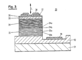
light beam source 21, e.g., a laser providing a beam of appropriate wavelength, emits a light pulse that reaches themodulator 10 via anoptical fiber 23, an opticaldirectional coupler 22 and afurther fiber 24 as indicated by the arrows. In themodulator 10, the light intensity of the beam is modulated in accordance with the data signals 27 applied as control signals Vc and retransmitted viafiber 24,coupler 22 andfiber 25 to the receivingstation 29. Here, the incoming light pulses are received by a light sensitive sensor, such as an optoelectronic photodetector, and, if necessary, restored to regenerate the data signalstream 28. - Fig. 3 shows a detailed cross-sectional representation of an
embodiment 30 of the inventive modulator. The device shown basically comprises the structural elements already described in connection with the conceptual structure illustrated in Fig. 1. - A semi-insulating (Si)
GaAs substrate 31 forms the basis on which the device is deposited. This substrate is covered with a n⁺GaAs buffer layer 32 having a thickness of 1 to 3 microns. It serves to provide a surface that is properly conditioned for the deposition of the ultra-thin alternate layers of thereflector structure 33.Reflector 33 consists, in the embodiment here described, of a sequence of 15 periods of alternate pairs of AlAs and GaxAl(1-x)As layers designated 33a and 33b, respectively. - The reflector structure corresponds to that of known λ/4 reflectors in which the optical thickness d of the
subsequent layers with λ = wavelength of light beam
n = refractive index of the layer material - For a wavelength λ of 0.8 micron and indices n = 3.0 for AlAs and n = 3.55 for Ga0.9Al0.1As one obtains for the AlAs layers 33a: d = 70.8 nm, and for the Ga0.9Al0.1As
layers 33b: d = 59.9 nm. - The total thickness dR of the stack of 15 periods forming the reflector then equals about
dR = 15 × (70.8 + 59.9) nm = about 2 micron. - In the embodiment of Fig. 3, the
absorber 34 is deposited on top of the reflector structure. Theabsorber 34 consists of a sequence of 100 periods of thin alternating GaAs (34a) and Ga0.7Al0.3As (34b) layers of 9.5 nm and 11 nm thickness, respectively. The GaAs layers form quantum wells which are separated by the GaAlAs layers. - Deposited on the upper surface of the absorber structure are p-type Ga0.9Al0.1As contact layers 35 and 36 of 150 nm and 50 nm thickness, respectively. The doping of p⁺ layer 35 is about 5·10¹⁷ to 2·10¹⁸ cm⁻³ whereas the doping of the heavier doped p⁺⁺
layer 36 is about 10²⁰ cm⁻³. Electrical contact to these layers is provided by patterned, ring-shapedmetallization 37 consisting of a Ti-Pt-Au layer of about 200 nm thickness. This metal layer defines the window of the modulator through which both, the incoming as well as the reflected light beam pass. This is illustrated by double arrow L. For proper optical fiber connections the window diameter is 50 to 100 microns. - The chosen thicknesses and p-doping concentrations of the contact layers 35 and 36 result in a low resistance ohmic contact with the
metal layer 37 and in a sufficiently uniform distribution of the electric field, that is created by voltage signals applied to the metal layer, over the whole cross-section of the modulator structure. - The device is topped with an antireflection coating 38 consisting of Si₃N₄ and having a thickness of about 100 nm which corresponds to the optical thickness of λ/4. This coating serves, in a well known manner, to reduce the reflection that would otherwise occur at the fiber-semiconductor interface.
- In the device illustrated in Fig. 3, the n-
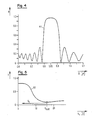
contact 39 is formed on the surface of a groove provided inbuffer layer 32.Contact 39 consists of an Au-Ge-Ni-Au layer of 80 nm thickness which, upon deposition, is alloyed (for 1 min. at 430°C) to form a low resistance ohmic contact with the semiconductor material. - In Fig. 4 the reflectivity R of the
reflector 33 of the modulator of Fig. 3 is plotted versus the wavelength λ of the light beam used. It shows that, for wavelength of λ = 0.85 micron, the reflectivity reaches the value of 0.97, i.e., 97% of the light arriving at thereflector 33 after passing through theabsorber 34 are reflected back - to once more pass through the absorber. - The diagram of Fig. 5 illustrates the operational characteristics of the modulator described above in connection with Fig. 3.
Curve 51 shows, for the modulator that consists of theabsorber 34 and thereflector 33, the transmission coefficient T plotted as a function of the voltage Vc applied between p- and n-type contacts absorber 34 in a reverse-biased condition. With a bias VBIAS as indicated in the diagram of Fig. 5, and with no data voltage signal Vs applied to thecontacts - As soon as a signal Vs of proper magnitude and polarity is applied to the contacts, where it is superimposed with the bias voltage VBIAS, the output intensity increases to about 80% of that of the incoming light beam. It follows, that the described modulator provides for a sufficiently high signal to noise ratio operation making the device well-suited for use, e.g., as a switch, in optical data transfer systems.
- The modulator structure hereinbefore described can be fabricated using technologies that are available and applying the knowledge and understanding disclosed in the art which is represented by the publications referred to in the introduction of the specification. Particularly, the molecular beam epitaxy (MBE) and the metal-organic chemical vapor deposition (MOCVD) processes have been developed to a point where the required ultra-thin layer structures can be produced in a single run, i.e., in the same vacuum without great difficulties and with sufficient accurateness, reliability and reproducibility. The other layers and elements of the described modulator structure can be fabricated using evaporation or epitaxy techniques, masking, patterning and etching processes that are well known in the art.
- The modulator structure of Fig. 3 represents only an example of a device in which the inventive concept, that has been described more generally in connection with Fig. 1, is implemented. Alternative structures, still based on the inventive concept, can be designed to serve particular requirements, e.g., by choosing different semiconductor materials, by using different dimensions and doping concentrations, or by changing the electrical contact and the optical interface design.
- For instance, the modulator may be structured to receive and to modulate not only light beams arriving on a single optical fiber but it may be extended to also handle multiple parallel beams arriving on a plurality of fibers. Matrix arrangements that may be advantageous, e.g., for picture processing applications, are also conceivable.
- In another alternative design, the
absorber 34 may consist of a so-called n-i-p-i doping superlattice structure rather than the quantum well arrangement that is used in the described embodiment. - Also, the n-
contact 39, in Fig. 3 arranged beside the multi-layer stack that comprises thereflector 33 and theabsorber 34, may be placed underneath thesubstrate 31 thus providing a simple structure, but abandoning certain packaging advantages inherent to a planar, mesa-type structure that can be fabricated on the same substrate as associated electronic circuitry. - Structural details may of course be changed as well. As an example, a thin patterned insulating layer (e.g. SiO₂ of 100 nm thickness) may be deposited underneath the n-
contact metal layer 37 in order to reduce the capacitance and thereby to improve the high speed performance of the device. - From the above, it will be evident that many other alternatives, modifications and variations still falling within the scope and spirit of the present invention will be apparent to those skilled in the art.
Claims (13)
- a semiconductor substrate (31),
- a reflector (33) consisting of a layered semiconductor structure epitaxially grown on one surface of said substrate, and
- an absorber (34) consisting of a semiconductor structure epitaxially grown on said reflector structure such that the intensity of a light beam (L), passing through the absorber before and after being reflected, can be modulated by means of electric control signals applied to contacts (37, 39) connecting to said modulator structure.
Priority Applications (3)
| Application Number | Priority Date | Filing Date | Title |
|---|---|---|---|
| DE8686108263T DE3681164D1 (en) | 1986-06-18 | 1986-06-18 | OPTOELECTRONIC VOLTAGE CONTROLLED MODULATOR. |
| EP86108263A EP0249645B1 (en) | 1986-06-18 | 1986-06-18 | Optoelectronic voltage-controlled modulator |
| JP62110915A JPS6324218A (en) | 1986-06-18 | 1987-05-08 | Voltage control type light modulator |
Applications Claiming Priority (1)
| Application Number | Priority Date | Filing Date | Title |
|---|---|---|---|
| EP86108263A EP0249645B1 (en) | 1986-06-18 | 1986-06-18 | Optoelectronic voltage-controlled modulator |
Publications (2)
| Publication Number | Publication Date |
|---|---|
| EP0249645A1 true EP0249645A1 (en) | 1987-12-23 |
| EP0249645B1 EP0249645B1 (en) | 1991-08-28 |
Family
ID=8195201
Family Applications (1)
| Application Number | Title | Priority Date | Filing Date |
|---|---|---|---|
| EP86108263A Expired - Lifetime EP0249645B1 (en) | 1986-06-18 | 1986-06-18 | Optoelectronic voltage-controlled modulator |
Country Status (3)
| Country | Link |
|---|---|
| EP (1) | EP0249645B1 (en) |
| JP (1) | JPS6324218A (en) |
| DE (1) | DE3681164D1 (en) |
Cited By (9)
| Publication number | Priority date | Publication date | Assignee | Title |
|---|---|---|---|---|
| US4915482A (en) * | 1988-10-27 | 1990-04-10 | International Business Machines Corporation | Optical modulator |
| GB2231969A (en) * | 1989-05-12 | 1990-11-28 | Stc Plc | Optical modulator |
| US5026148A (en) * | 1989-12-26 | 1991-06-25 | Hughes Aircraft Company | High efficiency multiple quantum well structure and operating method |
| WO1992000543A1 (en) * | 1990-06-29 | 1992-01-09 | The General Electric Company, Plc | Bipolar junction transistor combined with an optical modulator |
| US5202897A (en) * | 1990-05-25 | 1993-04-13 | British Telecommunications Public Limited Company | Fabry-perot modulator |
| US5426312A (en) * | 1989-02-23 | 1995-06-20 | British Telecommunications Public Limited Company | Fabry-perot modulator |
| US5488231A (en) * | 1994-11-23 | 1996-01-30 | Electronics And Telecommunications Research Institute | Metal/semiconductor junction Schottky diode optical device using a distortion grown layer |
| WO2002061498A1 (en) * | 2001-01-30 | 2002-08-08 | 3Dv Systems, Ltd. | Optical modulator |
| WO2011089243A1 (en) * | 2010-01-22 | 2011-07-28 | Vrije Universiteit Brussel | Evanescent wave absorption based devices |
Citations (2)
| Publication number | Priority date | Publication date | Assignee | Title |
|---|---|---|---|---|
| FR1603131A (en) * | 1968-07-05 | 1971-03-22 | ||
| WO1984003397A1 (en) * | 1983-02-28 | 1984-08-30 | American Telephone & Telegraph | Semiconductor device for controlling light using multiple quantum wells |
Family Cites Families (1)
| Publication number | Priority date | Publication date | Assignee | Title |
|---|---|---|---|---|
| JPS577418A (en) * | 1980-06-16 | 1982-01-14 | Takeda Chem Ind Ltd | Cephalosporin agent composition for oral administration |
-
1986
- 1986-06-18 EP EP86108263A patent/EP0249645B1/en not_active Expired - Lifetime
- 1986-06-18 DE DE8686108263T patent/DE3681164D1/en not_active Expired - Fee Related
-
1987
- 1987-05-08 JP JP62110915A patent/JPS6324218A/en active Granted
Patent Citations (2)
| Publication number | Priority date | Publication date | Assignee | Title |
|---|---|---|---|---|
| FR1603131A (en) * | 1968-07-05 | 1971-03-22 | ||
| WO1984003397A1 (en) * | 1983-02-28 | 1984-08-30 | American Telephone & Telegraph | Semiconductor device for controlling light using multiple quantum wells |
Non-Patent Citations (1)
| Title |
|---|
| JAPANESE JOURNAL OF APPLIED PHYSICS. SUPPLEMENTS 17TH CONF. ON SOLID-STATE DEVICES AND MATERIALS, 25th-27th August 1985, pages 91-94, Tokyo, JP; A. AJISAWA et al.: "Electric field induced absorption changes in InGaAsP/InP multi-quantum well" * |
Cited By (15)
| Publication number | Priority date | Publication date | Assignee | Title |
|---|---|---|---|---|
| US4915482A (en) * | 1988-10-27 | 1990-04-10 | International Business Machines Corporation | Optical modulator |
| US5426312A (en) * | 1989-02-23 | 1995-06-20 | British Telecommunications Public Limited Company | Fabry-perot modulator |
| GB2231969B (en) * | 1989-05-12 | 1993-11-03 | Stc Plc | Optical modulator |
| GB2231969A (en) * | 1989-05-12 | 1990-11-28 | Stc Plc | Optical modulator |
| US5017974A (en) * | 1989-05-12 | 1991-05-21 | Stc Plc | Optical modulator with superlattice having asymmetric barriers |
| US5026148A (en) * | 1989-12-26 | 1991-06-25 | Hughes Aircraft Company | High efficiency multiple quantum well structure and operating method |
| US5202897A (en) * | 1990-05-25 | 1993-04-13 | British Telecommunications Public Limited Company | Fabry-perot modulator |
| US5249074A (en) * | 1990-06-29 | 1993-09-28 | Gec-Marconi Limited | Bipolar junction transistor combined with an optical modulator |
| GB2245758B (en) * | 1990-06-29 | 1994-10-26 | Gen Electric Co Plc | A combined bipolar junction transistor and an optical modulator |
| WO1992000543A1 (en) * | 1990-06-29 | 1992-01-09 | The General Electric Company, Plc | Bipolar junction transistor combined with an optical modulator |
| US5488231A (en) * | 1994-11-23 | 1996-01-30 | Electronics And Telecommunications Research Institute | Metal/semiconductor junction Schottky diode optical device using a distortion grown layer |
| WO2002061498A1 (en) * | 2001-01-30 | 2002-08-08 | 3Dv Systems, Ltd. | Optical modulator |
| US6999219B2 (en) | 2001-01-30 | 2006-02-14 | 3Dv Systems, Ltd. | Optical modulator |
| WO2011089243A1 (en) * | 2010-01-22 | 2011-07-28 | Vrije Universiteit Brussel | Evanescent wave absorption based devices |
| US8921794B2 (en) | 2010-01-22 | 2014-12-30 | Vrije Universiteit Brussel | Evanescent wave absorption based devices |
Also Published As
| Publication number | Publication date |
|---|---|
| JPS6324218A (en) | 1988-02-01 |
| EP0249645B1 (en) | 1991-08-28 |
| DE3681164D1 (en) | 1991-10-02 |
| JPH0350247B2 (en) | 1991-08-01 |
Similar Documents
| Publication | Publication Date | Title |
|---|---|---|
| US5389797A (en) | Photodetector with absorbing region having resonant periodic absorption between reflectors | |
| JP3539977B2 (en) | Photoelectric semiconductor component | |
| US5202897A (en) | Fabry-perot modulator | |
| Miller | Optoelectronic applications of quantum wells | |
| US20060180830A1 (en) | Resonant cavity enhanced multi-quantum well light modulator and detector | |
| US5315430A (en) | Strained layer Fabry-Perot device | |
| EP0385685B1 (en) | Semiconductor device including cascaded modulation-doped quantum well heterostructures | |
| US5146078A (en) | Articles and systems comprising optically communicating logic elements including an electro-optical logic element | |
| US4818079A (en) | Multiple quantum well optical modulator | |
| JP2674626B2 (en) | Quantum well optical device | |
| EP0249645B1 (en) | Optoelectronic voltage-controlled modulator | |
| US5210428A (en) | Semiconductor device having shallow quantum well region | |
| US5027178A (en) | Electrically tunable interference filters and methods for their use | |
| JP2902501B2 (en) | Light modulation semiconductor device | |
| Kasper | Prospects and challenges of silicon/germanium on-chip optoelectronics | |
| US5412226A (en) | Semi-conductor structures | |
| Dutta | III-V device technologies for lightwave applications | |
| Goossen et al. | On the operational and manufacturing tolerances of GaAs-AlAs MQW modulators | |
| US6365430B1 (en) | Angle cavity resonant photodetector | |
| GB2378069A (en) | Vertically integrated optical transmitter and receiver | |
| JPS639163A (en) | Semiconductor photodetector | |
| JPH02199877A (en) | Optical receiver and photoelectric integrated circuit | |
| WO1993022839A1 (en) | Active optical logic device incorporating a surface-emitting laser | |
| Hu et al. | All-optical photonic switches using integrated inverted asymmetric Fabry-Perot modulators and heterojunction phototransistors | |
| EP0385638A2 (en) | Semiconductor superlattice self-electrooptic effect device |
Legal Events
| Date | Code | Title | Description |
|---|---|---|---|
| PUAI | Public reference made under article 153(3) epc to a published international application that has entered the european phase |
Free format text: ORIGINAL CODE: 0009012 |
|
| AK | Designated contracting states |
Kind code of ref document: A1 Designated state(s): DE FR GB IT |
|
| 17P | Request for examination filed |
Effective date: 19880426 |
|
| 17Q | First examination report despatched |
Effective date: 19900531 |
|
| GRAA | (expected) grant |
Free format text: ORIGINAL CODE: 0009210 |
|
| AK | Designated contracting states |
Kind code of ref document: B1 Designated state(s): DE FR GB IT |
|
| PG25 | Lapsed in a contracting state [announced via postgrant information from national office to epo] |
Ref country code: IT Free format text: LAPSE BECAUSE OF FAILURE TO SUBMIT A TRANSLATION OF THE DESCRIPTION OR TO PAY THE FEE WITHIN THE PRE;WARNING: LAPSES OF ITALIAN PATENTS WITH EFFECTIVE DATE BEFORE 2007 MAY HAVE OCCURRED AT ANY TIME BEFORE 2007. THE CORRECT EFFECTIVE DATE MAY BE DIFFERENT FROM THE ONE RECORDED.SCRIBED TIME-LIMIT Effective date: 19910828 |
|
| REF | Corresponds to: |
Ref document number: 3681164 Country of ref document: DE Date of ref document: 19911002 |
|
| ET | Fr: translation filed | ||
| PGFP | Annual fee paid to national office [announced via postgrant information from national office to epo] |
Ref country code: FR Payment date: 19920601 Year of fee payment: 7 |
|
| PGFP | Annual fee paid to national office [announced via postgrant information from national office to epo] |
Ref country code: DE Payment date: 19920619 Year of fee payment: 7 |
|
| PLBE | No opposition filed within time limit |
Free format text: ORIGINAL CODE: 0009261 |
|
| STAA | Information on the status of an ep patent application or granted ep patent |
Free format text: STATUS: NO OPPOSITION FILED WITHIN TIME LIMIT |
|
| 26N | No opposition filed | ||
| PG25 | Lapsed in a contracting state [announced via postgrant information from national office to epo] |
Ref country code: FR Effective date: 19940228 |
|
| PG25 | Lapsed in a contracting state [announced via postgrant information from national office to epo] |
Ref country code: DE Effective date: 19940301 |
|
| REG | Reference to a national code |
Ref country code: FR Ref legal event code: ST |
|
| PGFP | Annual fee paid to national office [announced via postgrant information from national office to epo] |
Ref country code: GB Payment date: 19950522 Year of fee payment: 10 |
|
| PG25 | Lapsed in a contracting state [announced via postgrant information from national office to epo] |
Ref country code: GB Effective date: 19960618 |
|
| GBPC | Gb: european patent ceased through non-payment of renewal fee |
Effective date: 19960618 |