EP0244052A2 - Programmable sampling time base circuit - Google Patents
Programmable sampling time base circuit Download PDFInfo
- Publication number
- EP0244052A2 EP0244052A2 EP87300794A EP87300794A EP0244052A2 EP 0244052 A2 EP0244052 A2 EP 0244052A2 EP 87300794 A EP87300794 A EP 87300794A EP 87300794 A EP87300794 A EP 87300794A EP 0244052 A2 EP0244052 A2 EP 0244052A2
- Authority
- EP
- European Patent Office
- Prior art keywords
- signal
- strobe
- trigger
- producing
- circuit
- Prior art date
- Legal status (The legal status is an assumption and is not a legal conclusion. Google has not performed a legal analysis and makes no representation as to the accuracy of the status listed.)
- Granted
Links
- 238000005070 sampling Methods 0.000 title abstract description 27
- 230000004044 response Effects 0.000 claims abstract description 22
- 238000001514 detection method Methods 0.000 claims abstract description 9
- 230000000737 periodic effect Effects 0.000 claims description 16
- 239000013078 crystal Substances 0.000 claims description 12
- 230000003252 repetitive effect Effects 0.000 claims description 6
- 230000000977 initiatory effect Effects 0.000 abstract description 3
- 238000005259 measurement Methods 0.000 description 5
- 238000000034 method Methods 0.000 description 5
- 230000003111 delayed effect Effects 0.000 description 4
- 230000000368 destabilizing effect Effects 0.000 description 3
- 230000008569 process Effects 0.000 description 3
- 238000012935 Averaging Methods 0.000 description 2
- 239000003990 capacitor Substances 0.000 description 2
- 238000010586 diagram Methods 0.000 description 2
- 238000012986 modification Methods 0.000 description 2
- 230000004048 modification Effects 0.000 description 2
- 230000005540 biological transmission Effects 0.000 description 1
- 230000001934 delay Effects 0.000 description 1
- 230000008520 organization Effects 0.000 description 1
- 230000001960 triggered effect Effects 0.000 description 1
Images
Classifications
-
- G—PHYSICS
- G01—MEASURING; TESTING
- G01R—MEASURING ELECTRIC VARIABLES; MEASURING MAGNETIC VARIABLES
- G01R13/00—Arrangements for displaying electric variables or waveforms
- G01R13/20—Cathode-ray oscilloscopes
- G01R13/22—Circuits therefor
- G01R13/32—Circuits for displaying non-recurrent functions such as transients; Circuits for triggering; Circuits for synchronisation; Circuits for time-base expansion
-
- G—PHYSICS
- G01—MEASURING; TESTING
- G01R—MEASURING ELECTRIC VARIABLES; MEASURING MAGNETIC VARIABLES
- G01R13/00—Arrangements for displaying electric variables or waveforms
- G01R13/20—Cathode-ray oscilloscopes
- G01R13/22—Circuits therefor
- G01R13/34—Circuits for representing a single waveform by sampling, e.g. for very high frequencies
- G01R13/345—Circuits for representing a single waveform by sampling, e.g. for very high frequencies for displaying sampled signals by using digital processors by intermediate A.D. and D.A. convertors (control circuits for CRT indicators)
Definitions
- the present invention relates in general to a time base circuit for producing a sampling strobe signal in a waveform sampling system and in par- - ticular to a time base circuit which provides for an accurately adjustable delay time between a triggering event and the strobe signal.
- Waveform sampling systems typically utilize a strobed sampling gate to sample an input waveform and it is desirable that a strobe signal controlling gate operation be generated a predetermined delay time following a triggering event, such as a zero crossing in the waveform being sampled.
- a triggering event such as a zero crossing in the waveform being sampled.
- an averaging sampling system samples a periodic waveform at a similar point along several repetitive sections of the waveform in order to determine an average value of the waveform at that point.
- each successive strobe signal should be generated at the same relative time with respect to a repetitive triggering event in each section of the waveform.
- an "equivalent time” sampling system samples several points at regular intervals along successive sections of a repetitive waveform by progressively increasing the strobe signal delay by regular, predetermined amounts after each repetitive triggering event in the waveform. This enables the sampling system to obtain samples representing several point along one cycle of the waveform even though the frequency of the waveform is relatively high compared to the sampling rate of the system.
- the accuracy of averaging and equivalent time sampling depends on the accuracy with which the delay between the triggering event and the sampling strobe signal can be controlled.
- the input waveform is applied to a trigger generator which produces a trigger signal on detection of the triggering event in the waveform.
- the trigger produced by the trigger recognizer is then delayed by a programmable delay circuit before being applied to a strobe signal generator and the strobe signal generator produces the strobe signal in response to the strobe drive signal.
- the time delay between the trigger signal and the strobe signal is controlled by programming the delay circuit, taking into account any inherent time delay in the operation of the trigger recognizer circuit.
- a time base circuit for a waveform sampling system produces a strobe signal an adjustable -strobe delay time following a triggering event in an input waveform to be sampled, the strobe signal controlling the time of input waveform sampling.
- the time base circuit includes a strobe control circuit for producing both the strobe signal and a strobe sense signal in response to a strobe drive signal.
- the time base circuit also includes a trigger generator for producing a trigger signal selectively either upon detection of the triggering event or upon detection of the strobe sense signal. The trigger signal is applied to a strobe drive circuit which produces the strobe drive signal an adjustable delay time following the trigger signal.
- the trigger generator initiates the trigger signal in response to the triggering event as the initiating event and the strobe drive circuit produces a single strobe drive signal in response to the trigger signal but delayed thereafter by an adjustable delay time.
- the strobe control circuit then generates a single strobe signal to initiate sampling of the input waveform.
- the trigger generator is set to produce the trigger signal in response to the strobe sense signal rather than in response to the triggering event.
- the trigger signal initiates a strobe drive signal, which in turn initiates another strobe sense signal which in turn initiates yet another trigger signal.
- the time-base circuit acts as an oscillator producing trigger, strobe drive and strobe sense signals periodically.
- the period between successive strobe drive signals is measured by a period timer which provides measurement data to a microprocessor and the microprocessor adjusts the delay time of the strobe drive circuit to adjust the period between successive strobe drive signals to a predetermined delay time.
- the strobe drive circuit includes a voltage controlled oscillator for generating a periodic output signal triggered by the trigger signal and a programmable counter for producing an output pulse an adjustable number of oscillator output signal cycles following the trigger signal.
- the counter output pulse is delayed by a programmable delay circuit to provide the strobe drive signal.
- the microprocessor grossly adjusts the strobe signal delay by adjusting the number of oscillator output signal cycles to be counted and finely adjusts the strobe signal delay by adjusting the pulse delay time of the programmable delay circuit.
- the period timer also measures the period of the voltage controlled oscillator output signal utilizing a crystal controlled oscillator as a references source.
- the microprocessor adjusts the voltage controlled oscillator frequency after each period measurement to compensate for frequency fluctuations due to ambient temperature changes and other destabilizing effects.
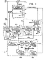
- FIG. 1 is a block diagram of a programmable time base circuit according to the present invention.
- a programmable time base circuit 10 depicted in block diagram form is adapted to produce a sampling strobe signal an adjustable delay time following a triggering event in an input waveform Vin.
- the strobe signal controls the operation of a sampling gate 12 which samples the input waveform Vin to produce an output waveform sample voltage Vo on receipt of the strobe signal.
- a sampling gate may be used,-for example, in a digital oscilloscope or a waveform digitizer to sample an input waveform at selected times relative to the triggering event.
- the time base circuit 10 includes a strobe control circuit 14 for producing both the strobe signal and a "strobe sense" signal in response to a "strobe drive” signal.
- the strobe control circuit 14 includes a strobe generator 15 adapted to produce a short strobe pulse on receipt of the strobe drive signal and a passive network 17 for producing the strobe sense signal.
- Network 17 includes a resistor 17a, and capacitors 17b and 17c connected in series to provide an AC path to ground for the strobe drive signal.
- the strobe sense signal is produced at the junction between the two capacitors in response to the strobe drive signal.
- the time base circuit 10 also includes a trigger generator 16 for producing a trigger signal (TRIG) selectively upon detection of a triggering event ("INT TRIG") in the input waveform Vin (an “internal trigger source”) upon detection of a triggering event (“EX TRIG”) in a waveform from an external trigger source, or upon detection of the strobe sense signal produced by the strobe control circuit 14.
- the trigger signal generated by the trigger generator 16 is applied as input to a strobe drive circuit 18 which produces the strobe drive signal an adjustable delay time following receipt of the trigger signal.
- the trigger generator 16 selects either the internal or the external trigger source to initiate the trigger signal upon detection of a triggering event and the strobe drive circuit 18 produces a single strobe drive signal following the trigger signal by a predetermined delay time.
- the strobe drive signal causes the strobe control circuit 14 to generate a single strobe pulse which in turn causes the gate 12 to sample the input waveform Vin.
- the time base circuit 10 includes provisions for calibrating the sample delay time between the triggering event and initiation of the strobe signal.
- the trigger generator 16 is set to produce the trigger signal in response to the strobe sense signal from the strobe control circuit 14 rather than in response to a triggering event in the internal or external trigger source.
- the trigger generator 16 produces an initial trigger signal to initiate a first strobe drive signal which in turn initiates a first strobe sense signal.
- the first strobe sense signal causes the trigger generator to generate a second trigger signal which in turn initiates a second strobe drive signal.
- the time base circuit 10 acts like an oscillator producing trigger, strobe drive and strobe sense signals periodically.
- the period between successive strobe drive signals is measured by a period timer 20 which provides data to a microprocessor (MPU) 22 indicating the period duration.
- the microprocessor 22 then adjusts the signal delay of the strobe drive circuit 18 according to the period data provided by the period timer 20 to calibrate the period between successive strobe signals to a predetermined delay time.
- the trigger generator 16 subsequently produces a trigger signal in response to a triggering event in the external or internal sources, the strobe signal follows the triggering event by the predetermined delay time.
- the delay time is regularly recalibrated in this fashion between sampling operations, fluctuations in strobe signal timing due to ambient temperature changes or other factors are substantially eliminated.
- the trigger generator 16 includes a trigger select circuit 24, a trigger recognizer 26, and a holdoff counter circuit 28.
- the external and internal trigger sources are applied as inputs to the trigger select circuit 24 which transmits a selected one of its inputs to the trigger recognizer 26 according to selection control signals (SEL) provided by a microprocessor 22.
- the trigger select circuit 24 also produces the first trigger signal during a calibration operation in response to a trigger control signal ("MPU TRIG") from the microprocessor 22.
- the trigger recognizer 26 suitably comprises a programmable level detector which produces the trigger signal as the output signal of the trigger select circuit 24 rises above or falls below a particular voltage level, the voltage level being predetermined by data from the microprocessor 22.
- the trigger signal output of the trigger recognizer 26 is applied as input to the holdoff counter circuit 28 causing the counter to reset its current count to zero, to begin transmitting an inhibit signal to the trigger recognizer 26, and to begin counting cycles of a periodic signal Vs generated by the strobe drive circuit 18.
- the inhibit signal prevents the trigger recognizer 26 from producing a subsequent trigger signal.
- the holdoff counter When the holdoff counter has counted a predetermined number of cycles of the Vs signal, it stops transmitting the inhibit signal to the trigger recognizer 26 and the trigger recognizer is thereupon armed to produce another trigger signal when it recognizes another triggering event.
- the count limit of the holdoff counter circuit 28 is set by data from the microprocessor 22 and is normally set high enough to ensure that a strobe signal is generated before the trigger generator produces another trigger .signal.
- the strobe drive circuit 18 includes a triggerable voltage controlled oscillator (VCO) 30, a programmable counter 32, a programmable delay circuit 34, and a digital to analog converter (DAC) 36.
- VCO 30 produces the previously mentioned periodic signal Vs of frequency controlled by the output voltage Vc of DAC 36.
- the magnitude of this control voltage Vc is determined by data from microprocessor 22 applied as input to DAC 36.
- the trigger signal from the trigger generator 16 "triggers" VCO 30 in that the trigger signal stops the VCO and restarts it, with predetermined phase, at a fixed time after the occurrence of the trigger signal.
- the trigger signal output of trigger generator 16 is also applied to a "clear" input of counter 32 and causes the counter to reset its current count to zero.
- the programmable counter 32 then counts cycles of the VCO 30 output signal Vs starting with the first cycle following the trigger signal and transmits an output pulse to the programmable delay circuit 34 when the number of Vs cycles counted reaches a predetermined count limit.
- the count limit is provided as input data to the programmable counter 32 from microprocessor 22.
- the programmable delay circuit 34 delays the output pulse produced by the programmable counter 32 by an adjustable amount, as determined by data from the microprocessor 22, and the delayed pulse output of the programmable delay circuit 34 is applied to the strobe control circuit 14 as the strobe drive signal output of the strobe drive circuit 18.
- the delay between the trigger signal and the strobe drive signal is equal to the count limit of the programmable counter 32 divided by the frequency of the output signal Vs of VCO 30 in combination with the delay of programmable delay circuit 34.
- the microprocessor 22 adjusts the count limit of programmable counter 32 and to finely adjust the delay, the microprocessor 22 adjusts the delay of programmable delay circuit 34.
- the microprocessor 22 switches the trigger select circuit 24 so that the strobe sense signal from the strobe control circuit 14 is applied to the trigger recognizer 26.
- the microprocessor 22 then transmits an MPU TRIG signal to the trigger select circuit 24, causing the trigger select circuit to transmit a pulse to the trigger recognizer 26.
- This pulse causes the trigger recognizer 26 to send a first trigger signal to the strobe drive circuit 18.
- the strobe drive circuit 18 produces a first strobe drive pulse. This first strobe drive pulse causes the strobe control circuit 14 to produce a first strobe sense pulse.
- the trigger select circuit 24 passes a strobe sense pulses to the trigger recognizer 26, the trigger recognizer generates a second trigger signal which causes the strobe drive circuit 18 to generate a second strobe pulse.
- the time base circuit 10 acts as an oscillator, periodically producing trigger, strobe drive and strobe sense signals.
- the period between strobe sense signals is substantially equal to the delay between a triggering event and a strobe signal when the trigger select circuit 24 is subsequently switched to select the internal or external trigger sources.
- the period timer 20 includes a frequency divider 37, a crystal oscillator 38, a gate circuit 40, and an event counter 42.
- the strobe drive signal is provided as input to the frequency divider 37 which drives its output signal low when it receives a first strobe drive signal pulse and drives its output high after it has received, for example, 1000 subsequent strobe drive signal pulses.
- a multiplexer 44 transmits the output signal of frequency divider 37 to a control input of gate 40 and another multiplexer 46 transmits the periodic output signal of the crystal oscillator 38 to a signal input of gate 40.
- gate 40 transmits the crystal oscillator output signal to event counter 42 and when the control input of gate 40 is driven high, the gate blocks transmission of the oscillator output signal to counter 42.
- the count in counter 42 and the operation of frequency divider 37 are reset by signals from the microprocessor 22 prior to a calibration operation.
- frequency divider 37 drives its output low causing gate 40 to connect the output signal of crystal oscillator 38 (suitably operating at approximately 200 MHz) to the input of the event counter 42.
- Event counter 42 then begins counting cycles of the crystal oscillator 38 output signal.
- frequency divider 37 drives its output high causing gate 40 to disconnect the oscillator 38 output signal from event counter 42.
- the microprocessor 22 reads the count in counter 42 and divides the count by 1000 and by the frequency of the output signal of crystal oscillator 38 to determine a strobe signal delay time resulting from the current adjustments of the programmable counter 32 and delay circuit 34 of the strobe drive circuit 18.
- the microprocessor 22 may then adjust the count limit of programmable counter 32, and/or the delay time of delay circuit 34 to increase or decrease the strobe signal delay time and may repeat the measurement and delay adjustment operations as necessary to accurately calibrate the strobe signal delay time to a predetermined value.
- the period timer 20 also enables the microprocessor 22 to calibrate the frequency of the triggerable VCO 30 of the strobe drive circuit 18.
- the output signal Vs of VCO 30 is connected to a second input of multiplexer 46.
- the output signal of crystal oscillator 38 is frequency divided (for instance by a factor of 10 6 ) by another frequency divider 48 and the output of frequency divider 48 is applied to a second input of multiplexer 44.
- the microprocessor 22 switches multiplexers 44 and 46 such that the output of frequency divider 48 controls the operation of gate 40 and such that Vs is applied as the signal input to gate 40.
- frequency divider 48 and counter 42 are reset by signals from microprocessor 22.
- frequency divider 48 Thereafter the output of frequency divider 48 is driven low for 10 6 cycles of crystal oscillator 38, enabling gate 40 to transmit Vs to event counter 42 for that time.
- the counter 42 counts cycles of Vs during that time and thereafter the microprocessor 42 reads the count, computes the VCO 30 output signal frequency from the count and alters the data applied to DAC 36 to adjust the VCO signal frequency.
- the measurement and adjustment process may continue iteratively until the VCO signal frequency is accurately calibrated.
- the programmable counter 32 and the programmable delay circuit 34 may be of the form described in co-pending Application Serial No.858,490 , filed April 30, 1986 (Attorney Docket No. USA 3906).
- the output signals provided by crystal oscillators are highly stable and are not strongly affected by changes in ambient temperature. Therefore the use of a crystal oscillator 38 to calibrate the strobe signal delay time and the VCO output frequency ensures consistency in timing circuit 10 calibration in spite of relatively large ambient temperature differences or other destabilizing effects between successive sampling operations.
Abstract
Description
- The present invention relates in general to a time base circuit for producing a sampling strobe signal in a waveform sampling system and in par- - ticular to a time base circuit which provides for an accurately adjustable delay time between a triggering event and the strobe signal.
- Waveform sampling systems typically utilize a strobed sampling gate to sample an input waveform and it is desirable that a strobe signal controlling gate operation be generated a predetermined delay time following a triggering event, such as a zero crossing in the waveform being sampled. For example an averaging sampling system samples a periodic waveform at a similar point along several repetitive sections of the waveform in order to determine an average value of the waveform at that point. To ensure that the waveform is sampled at the same point along each repetitive section of the waveform, each successive strobe signal should be generated at the same relative time with respect to a repetitive triggering event in each section of the waveform. As another example, an "equivalent time" sampling system samples several points at regular intervals along successive sections of a repetitive waveform by progressively increasing the strobe signal delay by regular, predetermined amounts after each repetitive triggering event in the waveform. This enables the sampling system to obtain samples representing several point along one cycle of the waveform even though the frequency of the waveform is relatively high compared to the sampling rate of the system.
- The accuracy of averaging and equivalent time sampling depends on the accuracy with which the delay between the triggering event and the sampling strobe signal can be controlled. In sampling system time base circuits of the prior art, the input waveform is applied to a trigger generator which produces a trigger signal on detection of the triggering event in the waveform. The trigger produced by the trigger recognizer is then delayed by a programmable delay circuit before being applied to a strobe signal generator and the strobe signal generator produces the strobe signal in response to the strobe drive signal. The time delay between the trigger signal and the strobe signal is controlled by programming the delay circuit, taking into account any inherent time delay in the operation of the trigger recognizer circuit. However the inherent operating time delay associated with the trigger generator and the programmable time delay of the delay circuit are influenced by ambient temperature fluctuations and therefore the timing of successive strobe signals with respect to successive triggering events can vary with time. What is needed and would be useful is a method and apparatus for continuously and rapidly recalibrating the sampling delay time.
- In accordance with one aspect of the invention, a time base circuit for a waveform sampling system produces a strobe signal an adjustable -strobe delay time following a triggering event in an input waveform to be sampled, the strobe signal controlling the time of input waveform sampling. The time base circuit includes a strobe control circuit for producing both the strobe signal and a strobe sense signal in response to a strobe drive signal. The time base circuit also includes a trigger generator for producing a trigger signal selectively either upon detection of the triggering event or upon detection of the strobe sense signal. The trigger signal is applied to a strobe drive circuit which produces the strobe drive signal an adjustable delay time following the trigger signal. During a sampling operation, the trigger generator initiates the trigger signal in response to the triggering event as the initiating event and the strobe drive circuit produces a single strobe drive signal in response to the trigger signal but delayed thereafter by an adjustable delay time. The strobe control circuit then generates a single strobe signal to initiate sampling of the input waveform.
- To calibrate the delay time between the triggering event and the strobe signal, the trigger generator is set to produce the trigger signal in response to the strobe sense signal rather than in response to the triggering event. The trigger signal initiates a strobe drive signal, which in turn initiates another strobe sense signal which in turn initiates yet another trigger signal. Thus, the time-base circuit acts as an oscillator producing trigger, strobe drive and strobe sense signals periodically. The period between successive strobe drive signals is measured by a period timer which provides measurement data to a microprocessor and the microprocessor adjusts the delay time of the strobe drive circuit to adjust the period between successive strobe drive signals to a predetermined delay time. When the timing circuit is calibrated in this fashion between sampling operations, fluctuations in strobe signal timing due to ambient temperature variations and other destabilizing effects are substantially eliminated.
- According to another aspect of the invention, the strobe drive circuit includes a voltage controlled oscillator for generating a periodic output signal triggered by the trigger signal and a programmable counter for producing an output pulse an adjustable number of oscillator output signal cycles following the trigger signal. The counter output pulse is delayed by a programmable delay circuit to provide the strobe drive signal. The microprocessor grossly adjusts the strobe signal delay by adjusting the number of oscillator output signal cycles to be counted and finely adjusts the strobe signal delay by adjusting the pulse delay time of the programmable delay circuit.
- According to a further aspect of the invention, the period timer also measures the period of the voltage controlled oscillator output signal utilizing a crystal controlled oscillator as a references source. The microprocessor adjusts the voltage controlled oscillator frequency after each period measurement to compensate for frequency fluctuations due to ambient temperature changes and other destabilizing effects.
- It is accordingly an object of the invention to provide a new and improved time base circuit for a waveform sampling system for providing a strobe signal an adjustable strobe signal delay time following a triggering event in a waveform to be sampled.
- It is another object of the invention to provide such a new and improved time base circuit wherein the strobe signal delay time may be accurately calibrated.
- The subject matter of the present invention is particularly pointed out and distinctly claimed in the concluding portion of this specification. However, both the organization and method of operation, together with further advantages and objects thereof, may best be understood by reference to the following description taken in connection with accompanying drawings.
- FIG. 1 is a block diagram of a programmable time base circuit according to the present invention.
- Referring to FIG. 1, a programmable
time base circuit 10, depicted in block diagram form is adapted to produce a sampling strobe signal an adjustable delay time following a triggering event in an input waveform Vin. The strobe signal controls the operation of asampling gate 12 which samples the input waveform Vin to produce an output waveform sample voltage Vo on receipt of the strobe signal. Such a sampling gate may be used,-for example, in a digital oscilloscope or a waveform digitizer to sample an input waveform at selected times relative to the triggering event. Thetime base circuit 10 includes astrobe control circuit 14 for producing both the strobe signal and a "strobe sense" signal in response to a "strobe drive" signal. Thestrobe control circuit 14 includes astrobe generator 15 adapted to produce a short strobe pulse on receipt of the strobe drive signal and apassive network 17 for producing the strobe sense signal.Network 17 includes aresistor 17a, andcapacitors - The
time base circuit 10 also includes atrigger generator 16 for producing a trigger signal (TRIG) selectively upon detection of a triggering event ("INT TRIG") in the input waveform Vin (an "internal trigger source") upon detection of a triggering event ("EX TRIG") in a waveform from an external trigger source, or upon detection of the strobe sense signal produced by thestrobe control circuit 14. The trigger signal generated by thetrigger generator 16 is applied as input to astrobe drive circuit 18 which produces the strobe drive signal an adjustable delay time following receipt of the trigger signal. - During a sampling operation, the
trigger generator 16 selects either the internal or the external trigger source to initiate the trigger signal upon detection of a triggering event and thestrobe drive circuit 18 produces a single strobe drive signal following the trigger signal by a predetermined delay time. The strobe drive signal causes thestrobe control circuit 14 to generate a single strobe pulse which in turn causes thegate 12 to sample the input waveform Vin. - The
time base circuit 10 includes provisions for calibrating the sample delay time between the triggering event and initiation of the strobe signal. During a calibration operation, thetrigger generator 16 is set to produce the trigger signal in response to the strobe sense signal from thestrobe control circuit 14 rather than in response to a triggering event in the internal or external trigger source. Thetrigger generator 16 produces an initial trigger signal to initiate a first strobe drive signal which in turn initiates a first strobe sense signal. The first strobe sense signal causes the trigger generator to generate a second trigger signal which in turn initiates a second strobe drive signal. As the process continues, thetime base circuit 10 acts like an oscillator producing trigger, strobe drive and strobe sense signals periodically. - The period between successive strobe drive signals is measured by a
period timer 20 which provides data to a microprocessor (MPU) 22 indicating the period duration. Themicroprocessor 22 then adjusts the signal delay of thestrobe drive circuit 18 according to the period data provided by theperiod timer 20 to calibrate the period between successive strobe signals to a predetermined delay time. When thetrigger generator 16 subsequently produces a trigger signal in response to a triggering event in the external or internal sources, the strobe signal follows the triggering event by the predetermined delay time. When the delay time is regularly recalibrated in this fashion between sampling operations, fluctuations in strobe signal timing due to ambient temperature changes or other factors are substantially eliminated. - The
trigger generator 16 includes a triggerselect circuit 24, atrigger recognizer 26, and aholdoff counter circuit 28. The external and internal trigger sources are applied as inputs to the triggerselect circuit 24 which transmits a selected one of its inputs to thetrigger recognizer 26 according to selection control signals (SEL) provided by amicroprocessor 22. The triggerselect circuit 24 also produces the first trigger signal during a calibration operation in response to a trigger control signal ("MPU TRIG") from themicroprocessor 22. The trigger recognizer 26 suitably comprises a programmable level detector which produces the trigger signal as the output signal of the triggerselect circuit 24 rises above or falls below a particular voltage level, the voltage level being predetermined by data from themicroprocessor 22. The trigger signal output of thetrigger recognizer 26 is applied as input to theholdoff counter circuit 28 causing the counter to reset its current count to zero, to begin transmitting an inhibit signal to thetrigger recognizer 26, and to begin counting cycles of a periodic signal Vs generated by thestrobe drive circuit 18. The inhibit signal prevents the trigger recognizer 26 from producing a subsequent trigger signal. When the holdoff counter has counted a predetermined number of cycles of the Vs signal, it stops transmitting the inhibit signal to thetrigger recognizer 26 and the trigger recognizer is thereupon armed to produce another trigger signal when it recognizes another triggering event. The count limit of theholdoff counter circuit 28 is set by data from themicroprocessor 22 and is normally set high enough to ensure that a strobe signal is generated before the trigger generator produces another trigger .signal. - The
strobe drive circuit 18 includes a triggerable voltage controlled oscillator (VCO) 30, aprogrammable counter 32, aprogrammable delay circuit 34, and a digital to analog converter (DAC) 36. TheVCO 30 produces the previously mentioned periodic signal Vs of frequency controlled by the output voltage Vc ofDAC 36. The magnitude of this control voltage Vc is determined by data frommicroprocessor 22 applied as input toDAC 36. The trigger signal from thetrigger generator 16 "triggers"VCO 30 in that the trigger signal stops the VCO and restarts it, with predetermined phase, at a fixed time after the occurrence of the trigger signal. The trigger signal output oftrigger generator 16 is also applied to a "clear" input ofcounter 32 and causes the counter to reset its current count to zero. Theprogrammable counter 32 then counts cycles of theVCO 30 output signal Vs starting with the first cycle following the trigger signal and transmits an output pulse to theprogrammable delay circuit 34 when the number of Vs cycles counted reaches a predetermined count limit. The count limit is provided as input data to theprogrammable counter 32 frommicroprocessor 22. Theprogrammable delay circuit 34 delays the output pulse produced by theprogrammable counter 32 by an adjustable amount, as determined by data from themicroprocessor 22, and the delayed pulse output of theprogrammable delay circuit 34 is applied to thestrobe control circuit 14 as the strobe drive signal output of thestrobe drive circuit 18. - The delay between the trigger signal and the strobe drive signal is equal to the count limit of the
programmable counter 32 divided by the frequency of the output signal Vs ofVCO 30 in combination with the delay ofprogrammable delay circuit 34. To grossly adjust the delay between the trigger signal and the strobe drive signal, themicroprocessor 22 adjusts the count limit ofprogrammable counter 32 and to finely adjust the delay, themicroprocessor 22 adjusts the delay ofprogrammable delay circuit 34. - When the delay between the triggering event and the strobe signal is to be measured for calibration purposes, the
microprocessor 22 switches the triggerselect circuit 24 so that the strobe sense signal from thestrobe control circuit 14 is applied to thetrigger recognizer 26. Themicroprocessor 22 then transmits an MPU TRIG signal to the triggerselect circuit 24, causing the trigger select circuit to transmit a pulse to thetrigger recognizer 26. This pulse causes thetrigger recognizer 26 to send a first trigger signal to thestrobe drive circuit 18. After a delay determined by the count limit ofprogrammable counter 32 and the programmable delay ofdelay circuit 34, thestrobe drive circuit 18 produces a first strobe drive pulse. This first strobe drive pulse causes thestrobe control circuit 14 to produce a first strobe sense pulse. Since the triggerselect circuit 24 passes a strobe sense pulses to thetrigger recognizer 26, the trigger recognizer generates a second trigger signal which causes thestrobe drive circuit 18 to generate a second strobe pulse. As the process continues thetime base circuit 10 acts as an oscillator, periodically producing trigger, strobe drive and strobe sense signals. The period between strobe sense signals is substantially equal to the delay between a triggering event and a strobe signal when the triggerselect circuit 24 is subsequently switched to select the internal or external trigger sources. - The
period timer 20 includes afrequency divider 37, acrystal oscillator 38, agate circuit 40, and anevent counter 42. The strobe drive signal is provided as input to thefrequency divider 37 which drives its output signal low when it receives a first strobe drive signal pulse and drives its output high after it has received, for example, 1000 subsequent strobe drive signal pulses. Amultiplexer 44 transmits the output signal offrequency divider 37 to a control input ofgate 40 and anothermultiplexer 46 transmits the periodic output signal of thecrystal oscillator 38 to a signal input ofgate 40. When the control input ofgate 40 is driven low,gate 40 transmits the crystal oscillator output signal toevent counter 42 and when the control input ofgate 40 is driven high, the gate blocks transmission of the oscillator output signal to counter 42. - The count in
counter 42 and the operation offrequency divider 37 are reset by signals from themicroprocessor 22 prior to a calibration operation. After the first strobe drive pulse is generated,frequency divider 37 drives its outputlow causing gate 40 to connect the output signal of crystal oscillator 38 (suitably operating at approximately 200 MHz) to the input of theevent counter 42.Event counter 42 then begins counting cycles of thecrystal oscillator 38 output signal. After 1000 more strobe drive pulses have been generated by thestrobe drive circuit 18,frequency divider 37 drives its outputhigh causing gate 40 to disconnect theoscillator 38 output signal fromevent counter 42. Thereafter themicroprocessor 22 reads the count incounter 42 and divides the count by 1000 and by the frequency of the output signal ofcrystal oscillator 38 to determine a strobe signal delay time resulting from the current adjustments of theprogrammable counter 32 anddelay circuit 34 of thestrobe drive circuit 18. Themicroprocessor 22 may then adjust the count limit ofprogrammable counter 32, and/or the delay time ofdelay circuit 34 to increase or decrease the strobe signal delay time and may repeat the measurement and delay adjustment operations as necessary to accurately calibrate the strobe signal delay time to a predetermined value. - The
period timer 20 also enables themicroprocessor 22 to calibrate the frequency of thetriggerable VCO 30 of thestrobe drive circuit 18. The output signal Vs ofVCO 30 is connected to a second input ofmultiplexer 46. The output signal ofcrystal oscillator 38 is frequency divided (for instance by a factor of 106) by anotherfrequency divider 48 and the output offrequency divider 48 is applied to a second input ofmultiplexer 44. To calibrate the frequency of the triggerable VCO output signal, themicroprocessor 22 switches multiplexers 44 and 46 such that the output offrequency divider 48 controls the operation ofgate 40 and such that Vs is applied as the signal input togate 40. Prior to a measurement operation,frequency divider 48 and counter 42 are reset by signals frommicroprocessor 22. Thereafter the output offrequency divider 48 is driven low for 10 6 cycles ofcrystal oscillator 38, enablinggate 40 to transmit Vs toevent counter 42 for that time. The counter 42 counts cycles of Vs during that time and thereafter themicroprocessor 42 reads the count, computes theVCO 30 output signal frequency from the count and alters the data applied toDAC 36 to adjust the VCO signal frequency. The measurement and adjustment process may continue iteratively until the VCO signal frequency is accurately calibrated. - The
programmable counter 32 and theprogrammable delay circuit 34 may be of the form described in co-pending Application Serial No.858,490 , filed April 30, 1986 (Attorney Docket No. USA 3906). - The output signals provided by crystal oscillators are highly stable and are not strongly affected by changes in ambient temperature. Therefore the use of a
crystal oscillator 38 to calibrate the strobe signal delay time and the VCO output frequency ensures consistency intiming circuit 10 calibration in spite of relatively large ambient temperature differences or other destabilizing effects between successive sampling operations. - While a preferred embodiment of the present invention has been shown and described, it will be apparent to those skilled in the art that many changes and modifications may be made without departing from the invention in its broader aspects. The appended claims are therefore intended to cover all such changes and modifications as fall within the true spirit and scope of the invention.
Claims (7)
Applications Claiming Priority (2)
| Application Number | Priority Date | Filing Date | Title |
|---|---|---|---|
| US06/858,490 US4812769A (en) | 1986-04-30 | 1986-04-30 | Programmable sampling time base circuit |
| US858490 | 1986-04-30 |
Publications (3)
| Publication Number | Publication Date |
|---|---|
| EP0244052A2 true EP0244052A2 (en) | 1987-11-04 |
| EP0244052A3 EP0244052A3 (en) | 1989-02-08 |
| EP0244052B1 EP0244052B1 (en) | 1993-08-11 |
Family
ID=25328436
Family Applications (1)
| Application Number | Title | Priority Date | Filing Date |
|---|---|---|---|
| EP87300794A Expired - Lifetime EP0244052B1 (en) | 1986-04-30 | 1987-01-29 | Programmable sampling time base circuit |
Country Status (4)
| Country | Link |
|---|---|
| US (1) | US4812769A (en) |
| EP (1) | EP0244052B1 (en) |
| JP (1) | JPS62261964A (en) |
| DE (1) | DE3786945T2 (en) |
Cited By (4)
| Publication number | Priority date | Publication date | Assignee | Title |
|---|---|---|---|---|
| EP0425737A1 (en) * | 1989-10-30 | 1991-05-08 | Tektronix Uk Ltd. | Digital storage oscilloscopes |
| EP0539129A1 (en) * | 1991-10-21 | 1993-04-28 | Tektronix, Inc. | Detection of metastability in triggers |
| NL9301502A (en) * | 1993-02-22 | 1994-09-16 | Hewlett Packard Co | Pseudo-random repeated sampling of a signal. |
| GB2329311A (en) * | 1997-09-11 | 1999-03-17 | Hewlett Packard Co | Sampling timebase system |
Families Citing this family (33)
| Publication number | Priority date | Publication date | Assignee | Title |
|---|---|---|---|---|
| US5054490A (en) * | 1988-05-11 | 1991-10-08 | Lunar Corporation | Ultrasonic densitometer device and method |
| US5446650A (en) * | 1993-10-12 | 1995-08-29 | Tektronix, Inc. | Logic signal extraction |
| US6181267B1 (en) | 1998-09-30 | 2001-01-30 | Agilent Technologies Inc. | Internally triggered equivalent-time sampling system for signals having a predetermined data rate |
| US6317842B1 (en) | 1999-02-16 | 2001-11-13 | Qlogic Corporation | Method and circuit for receiving dual edge clocked data |
| US6615345B1 (en) * | 1999-07-29 | 2003-09-02 | Micron Technology, Inc. | System and method for regulating data capture in response to data strobe using preamble, postamble and strobe signature |
| US6564160B2 (en) * | 2001-06-22 | 2003-05-13 | Agilent Technologies, Inc. | Random sampling with phase measurement |
| US7111228B1 (en) | 2002-05-07 | 2006-09-19 | Marvell International Ltd. | System and method for performing parity checks in disk storage system |
| US7007114B1 (en) | 2003-01-31 | 2006-02-28 | Qlogic Corporation | System and method for padding data blocks and/or removing padding from data blocks in storage controllers |
| US7287102B1 (en) | 2003-01-31 | 2007-10-23 | Marvell International Ltd. | System and method for concatenating data |
| US7064915B1 (en) | 2003-03-10 | 2006-06-20 | Marvell International Ltd. | Method and system for collecting servo field data from programmable devices in embedded disk controllers |
| US7457903B2 (en) * | 2003-03-10 | 2008-11-25 | Marvell International Ltd. | Interrupt controller for processing fast and regular interrupts |
| US7039771B1 (en) | 2003-03-10 | 2006-05-02 | Marvell International Ltd. | Method and system for supporting multiple external serial port devices using a serial port controller in embedded disk controllers |
| US7099963B2 (en) * | 2003-03-10 | 2006-08-29 | Qlogic Corporation | Method and system for monitoring embedded disk controller components |
| US7492545B1 (en) | 2003-03-10 | 2009-02-17 | Marvell International Ltd. | Method and system for automatic time base adjustment for disk drive servo controllers |
| US7870346B2 (en) * | 2003-03-10 | 2011-01-11 | Marvell International Ltd. | Servo controller interface module for embedded disk controllers |
| US7339984B1 (en) | 2003-04-10 | 2008-03-04 | Agilent Technologies, Inc. | Method and apparatus for jitter measurement using phase and amplitude undersampling |
| US7526691B1 (en) | 2003-10-15 | 2009-04-28 | Marvell International Ltd. | System and method for using TAP controllers |
| US7284141B2 (en) * | 2004-02-05 | 2007-10-16 | Anritsu Company | Method of and apparatus for measuring jitter and generating an eye diagram of a high speed data signal |
| US7139150B2 (en) * | 2004-02-10 | 2006-11-21 | Marvell International Ltd. | Method and system for head position control in embedded disk drive controllers |
| US7120084B2 (en) * | 2004-06-14 | 2006-10-10 | Marvell International Ltd. | Integrated memory controller |
| US8166217B2 (en) * | 2004-06-28 | 2012-04-24 | Marvell International Ltd. | System and method for reading and writing data using storage controllers |
| US7757009B2 (en) | 2004-07-19 | 2010-07-13 | Marvell International Ltd. | Storage controllers with dynamic WWN storage modules and methods for managing data and connections between a host and a storage device |
| US8032674B2 (en) * | 2004-07-19 | 2011-10-04 | Marvell International Ltd. | System and method for controlling buffer memory overflow and underflow conditions in storage controllers |
| US9201599B2 (en) * | 2004-07-19 | 2015-12-01 | Marvell International Ltd. | System and method for transmitting data in storage controllers |
| US7386661B2 (en) | 2004-10-13 | 2008-06-10 | Marvell International Ltd. | Power save module for storage controllers |
| US7240267B2 (en) * | 2004-11-08 | 2007-07-03 | Marvell International Ltd. | System and method for conducting BIST operations |
| US7802026B2 (en) * | 2004-11-15 | 2010-09-21 | Marvell International Ltd. | Method and system for processing frames in storage controllers |
| US7609468B2 (en) | 2005-04-06 | 2009-10-27 | Marvell International Ltd. | Method and system for read gate timing control for storage controllers |
| US20060241915A1 (en) * | 2005-04-08 | 2006-10-26 | Woodward Mark J | Quadrature phase-shifting timebase system |
| US8654548B2 (en) * | 2010-12-06 | 2014-02-18 | Semtech Corporation | Flyback primary side output voltage sensing system and method |
| US10090057B2 (en) | 2017-02-23 | 2018-10-02 | Sandisk Technologies Llc | Dynamic strobe timing |
| US10534018B1 (en) | 2019-01-16 | 2020-01-14 | Guzik Technical Enterprises | Time base correction method for high accuracy sampling scope-based measurements |
| CN114509589A (en) * | 2020-11-17 | 2022-05-17 | 北京普源精电科技有限公司 | Oscilloscope trigger system, oscilloscope trigger method, oscilloscope and storage medium |
Citations (3)
| Publication number | Priority date | Publication date | Assignee | Title |
|---|---|---|---|---|
| JPS5935155A (en) * | 1982-08-23 | 1984-02-25 | Tohoku Denshi Sangyo Kk | Apparatus for measuring high speed phenomenon |
| EP0119616A2 (en) * | 1983-03-23 | 1984-09-26 | Tektronix, Inc. | Programmable delay circuit |
| US4504749A (en) * | 1981-07-20 | 1985-03-12 | Takeda Riken Co., Ltd. | Delay pulse generating circuit |
Family Cites Families (4)
| Publication number | Priority date | Publication date | Assignee | Title |
|---|---|---|---|---|
| US3646370A (en) * | 1970-07-06 | 1972-02-29 | Honeywell Inc | Stabilized monostable delay multivibrator or one-shot apparatus |
| US4415861A (en) * | 1981-06-08 | 1983-11-15 | Tektronix, Inc. | Programmable pulse generator |
| JPS603561A (en) * | 1983-06-20 | 1985-01-09 | Nissan Motor Co Ltd | Frequency discriminating circuit |
| US4717883A (en) * | 1986-08-04 | 1988-01-05 | Analog Devices, Inc. | Method and apparatus for reducing errors in a sampling system utilizing an error-sampled feedback loop |
-
1986
- 1986-04-30 US US06/858,490 patent/US4812769A/en not_active Expired - Lifetime
-
1987
- 1987-01-29 DE DE87300794T patent/DE3786945T2/en not_active Expired - Fee Related
- 1987-01-29 EP EP87300794A patent/EP0244052B1/en not_active Expired - Lifetime
- 1987-04-17 JP JP62095010A patent/JPS62261964A/en active Granted
Patent Citations (3)
| Publication number | Priority date | Publication date | Assignee | Title |
|---|---|---|---|---|
| US4504749A (en) * | 1981-07-20 | 1985-03-12 | Takeda Riken Co., Ltd. | Delay pulse generating circuit |
| JPS5935155A (en) * | 1982-08-23 | 1984-02-25 | Tohoku Denshi Sangyo Kk | Apparatus for measuring high speed phenomenon |
| EP0119616A2 (en) * | 1983-03-23 | 1984-09-26 | Tektronix, Inc. | Programmable delay circuit |
Non-Patent Citations (4)
| Title |
|---|
| ELECTRONICS ENGINEERING, vol. 56, no. 692, August 1984, page 12, Southend-on-Sea, Essex, GB; C.W.FOTHERBY: "Mystery 'scope front end - a reader's design" * |
| ELEKTRONIK, vol. 25, no. 11, November 1976, pages 115-117; V.DOLCH: "Oszilloskop-Zusatzgerät ermöglicht Trigger-Verzögerung nach Zeit und Ereignis" * |
| PATENT ABSTRACTS OF JAPAN, vol. 8, no. 133 (P-281)[1570], 20th June 1984; & JP-A-59 035 155 (TOUHOKU DENSHI SANGYO K.K.) 25-02-1984 * |
| ULTRASONICS, vol. 11, no. 4, July 1973, pages 165-173; S.LEES et al.: "DONAR: a computer processing system to extend ultrasonic pulse-echo testing" * |
Cited By (4)
| Publication number | Priority date | Publication date | Assignee | Title |
|---|---|---|---|---|
| EP0425737A1 (en) * | 1989-10-30 | 1991-05-08 | Tektronix Uk Ltd. | Digital storage oscilloscopes |
| EP0539129A1 (en) * | 1991-10-21 | 1993-04-28 | Tektronix, Inc. | Detection of metastability in triggers |
| NL9301502A (en) * | 1993-02-22 | 1994-09-16 | Hewlett Packard Co | Pseudo-random repeated sampling of a signal. |
| GB2329311A (en) * | 1997-09-11 | 1999-03-17 | Hewlett Packard Co | Sampling timebase system |
Also Published As
| Publication number | Publication date |
|---|---|
| EP0244052A3 (en) | 1989-02-08 |
| DE3786945D1 (en) | 1993-09-16 |
| EP0244052B1 (en) | 1993-08-11 |
| JPH0573176B2 (en) | 1993-10-13 |
| DE3786945T2 (en) | 1994-02-10 |
| JPS62261964A (en) | 1987-11-14 |
| US4812769A (en) | 1989-03-14 |
Similar Documents
| Publication | Publication Date | Title |
|---|---|---|
| US4812769A (en) | Programmable sampling time base circuit | |
| EP0244537B1 (en) | Equivalent time pseudorandom sampling system | |
| US5959479A (en) | Sampling timebase system | |
| JPH0261811B2 (en) | ||
| EP0103393A1 (en) | Inductive loop vehicle detector | |
| US4637733A (en) | High-resolution electronic chronometry system | |
| JPH056151B2 (en) | ||
| US5463639A (en) | Automatic pattern synchronizing circuit of an error detector | |
| US4968907A (en) | Digital delay generator | |
| US4118698A (en) | Analog-to-digital converter recalibration method and apparatus | |
| US4736351A (en) | Precision semiconductor device timer | |
| EP0123039B1 (en) | Signal detector | |
| US4208626A (en) | Precision timing source for multiple rate sampling of high-speed waveforms | |
| US3979715A (en) | Method and system for achieving vibrator phase lock | |
| EP0182999B1 (en) | Self-arming, prescaling frequency counter system | |
| US2939075A (en) | Delay calibrating apparatus | |
| US4251777A (en) | Method of and apparatus for time-stabilization of sampling pulses | |
| US4868465A (en) | Sweep generator error characterization | |
| US3524993A (en) | Triggering method and apparatus wherein the triggering period is determined | |
| US3965431A (en) | Circuitry for producing pulses with precise predetermined widths | |
| US3509473A (en) | Time measuring system | |
| EP0087874A2 (en) | Apparatus and method for generating pretrigger and trigger signals | |
| US4999573A (en) | Method and apparatus for measurement gate display | |
| US2829250A (en) | Repetition-period limiter | |
| US4386322A (en) | Method and apparatus for producing a trigger signal |
Legal Events
| Date | Code | Title | Description |
|---|---|---|---|
| PUAI | Public reference made under article 153(3) epc to a published international application that has entered the european phase |
Free format text: ORIGINAL CODE: 0009012 |
|
| AK | Designated contracting states |
Kind code of ref document: A2 Designated state(s): DE FR GB NL |
|
| PUAL | Search report despatched |
Free format text: ORIGINAL CODE: 0009013 |
|
| AK | Designated contracting states |
Kind code of ref document: A3 Designated state(s): DE FR GB NL |
|
| 17P | Request for examination filed |
Effective date: 19890715 |
|
| 17Q | First examination report despatched |
Effective date: 19911202 |
|
| GRAA | (expected) grant |
Free format text: ORIGINAL CODE: 0009210 |
|
| AK | Designated contracting states |
Kind code of ref document: B1 Designated state(s): DE FR GB NL |
|
| PG25 | Lapsed in a contracting state [announced via postgrant information from national office to epo] |
Ref country code: NL Effective date: 19930811 |
|
| ET | Fr: translation filed | ||
| REF | Corresponds to: |
Ref document number: 3786945 Country of ref document: DE Date of ref document: 19930916 |
|
| NLV1 | Nl: lapsed or annulled due to failure to fulfill the requirements of art. 29p and 29m of the patents act | ||
| PLBE | No opposition filed within time limit |
Free format text: ORIGINAL CODE: 0009261 |
|
| STAA | Information on the status of an ep patent application or granted ep patent |
Free format text: STATUS: NO OPPOSITION FILED WITHIN TIME LIMIT |
|
| 26N | No opposition filed | ||
| PG25 | Lapsed in a contracting state [announced via postgrant information from national office to epo] |
Ref country code: FR Effective date: 19940930 |
|
| REG | Reference to a national code |
Ref country code: FR Ref legal event code: ST |
|
| PGFP | Annual fee paid to national office [announced via postgrant information from national office to epo] |
Ref country code: GB Payment date: 19951219 Year of fee payment: 10 |
|
| PGFP | Annual fee paid to national office [announced via postgrant information from national office to epo] |
Ref country code: DE Payment date: 19951220 Year of fee payment: 10 |
|
| PG25 | Lapsed in a contracting state [announced via postgrant information from national office to epo] |
Ref country code: GB Effective date: 19970129 |
|
| GBPC | Gb: european patent ceased through non-payment of renewal fee |
Effective date: 19970129 |
|
| PG25 | Lapsed in a contracting state [announced via postgrant information from national office to epo] |
Ref country code: DE Effective date: 19971001 |