EP0232437B1 - Multiplex interface for a communication controller - Google Patents
Multiplex interface for a communication controller Download PDFInfo
- Publication number
- EP0232437B1 EP0232437B1 EP85430041A EP85430041A EP0232437B1 EP 0232437 B1 EP0232437 B1 EP 0232437B1 EP 85430041 A EP85430041 A EP 85430041A EP 85430041 A EP85430041 A EP 85430041A EP 0232437 B1 EP0232437 B1 EP 0232437B1
- Authority
- EP
- European Patent Office
- Prior art keywords
- data
- bits
- bit
- control
- line
- Prior art date
- Legal status (The legal status is an assumption and is not a legal conclusion. Google has not performed a legal analysis and makes no representation as to the accuracy of the status listed.)
- Expired
Links
Images


Classifications
-
- H—ELECTRICITY
- H04—ELECTRIC COMMUNICATION TECHNIQUE
- H04L—TRANSMISSION OF DIGITAL INFORMATION, e.g. TELEGRAPHIC COMMUNICATION
- H04L12/00—Data switching networks
- H04L12/50—Circuit switching systems, i.e. systems in which the path is physically permanent during the communication
- H04L12/52—Circuit switching systems, i.e. systems in which the path is physically permanent during the communication using time division techniques
- H04L12/525—Circuit switching systems, i.e. systems in which the path is physically permanent during the communication using time division techniques involving a stored program control
-
- G—PHYSICS
- G06—COMPUTING; CALCULATING OR COUNTING
- G06F—ELECTRIC DIGITAL DATA PROCESSING
- G06F13/00—Interconnection of, or transfer of information or other signals between, memories, input/output devices or central processing units
- G06F13/38—Information transfer, e.g. on bus
- G06F13/40—Bus structure
- G06F13/4004—Coupling between buses
- G06F13/4022—Coupling between buses using switching circuits, e.g. switching matrix, connection or expansion network
Definitions
- This invention relates to a multiplex interface for the line scanners of a communication controller, allowing the communication controller to be connected to any type of physical or logical attachments.
- the communication controller may be connected to physical attachments such as modems or network standard data interfaces such as V24, V35, Bell 303, X21 or any local attached interface working at any speed or to logical attachments such as Time Division Multiplex links (T1, CEPT (Confrete Europeenne des Postes et Telecommunications) first order mutliplex, Integrated Service Digital Network ISDN basic access, ISDN extended access) or to PBX interfaces.
- T1 Time Division Multiplex links
- CEPT Confimpulses et Telecommunications
- mutliplex Integrated Service Digital Network ISDN basic access
- ISDN extended access ISDN extended access
- Patent Application EP-A 0 077 863 describes a line adapter to be used in a communication controller.
- This line adapter presents one drawback. Since it has to be connected to a plurality of users through line connectors having a quite large size, the adapters are distant from each others and thus the bus-connecting them to the Central Control Unit is long which causes the transit delays on the bus to be long and the performances of the Communication Controller to be degraded.
- EP-A 0 016 426 In the digital telephone exchange field, it is known from EP-A 0 016 426 to allocate a channel at a given rate (64 Kbit/s) for the speech and one at an equal rate for the signalling to each subscriber which has access to the connection network.
- An object of this invention is to provide the line scanners of the communication controller with a multiplex interface which allows the communication controller to be connected to any type of users.
- Another object of the invention is to provide such a multiplex interface which allows the performance of the communication controller to be improved.
- the multiplex interface according to the invention as set forth in claim 1 is to be connected to the scanning means of a communication controller in order to exchange data and control bits between the line scanning means and the user attached to the communication controller.
- the data and control bits are carried in data and control slots respectively, said slots having specific structures which give the communicating controller its versatility.
- the interface comprises transmit and receive synchronous multiplex links connecting the line scanning means to the users through multiplexing means, the data and control bits being exchanged on the transmit and receive multiplex links in synchronous frames wherein at least one data slot and one control slot are assigned to each user, the structures of the two slots being identical for all types of users.
- the data slot comprises n bits which include a variable number x of valid bits depending upon the line speed of the user information carrying medium (line or multiplex link) assigned to the data slot, said number being indicated by a variable delimitation pattern comprising a first delimiting bit set at a first binary value (1) adjacent to the data bits and (n-x-1) bits set at the second binary value (0) adjacent to said first delimiting bit.
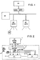
- a communication controller comprises as schematically represented in figure 1, a central control unit CCU connected on the one hand to communication lines through line adapters and on the other hand to central processing units through channel adapters.
- the line adapters serve at least one user line by means of a cyclic scanning device and a random access memory assembly containing the data received or to be sent on the various lines as controlled by the scanning device.
- the line adapter according to the present invention is schematically shown in figure 2. It is comprised of line scanning means 1 which are similar to the line scanning means such as described in above patent application except that a full duplex link 3 is provided at the output of the line scanning means.
- a slot or a plurality of slots, is assigned to each user connected to the adapter so that the data and control bits from/to the line users are exchanged in said slots on synchronous links 3R and 3T.
- the succession of slots assigned to the users attached to an adapter constitutes a frame.
- Link 3 is connected to multiplexing device 5 which generates from the bits received from line scanning means 1, a frame synchronization signal on line 7 and a bit clock signal of line 9 and transmits the data and control bits from the transmit link 3-T to line interface circuits LIC 11 through line 13. It is assumed that there are eight LIC circuits numbered 11-1 to 11-8. This allows to attach from one line at up to 2 megabits per second to thirty two physical or logical channels at up to 64 kilobits per second.
- the bits received from the users through line interface circuits 11 are transmitted to multiplexing circuit 5 which provides them through receive link 3-R, to line scanning means 1.
- line interface circuits 11 may be apart from the communication controller in a separate active tail gate enclosure 17.
- transit delay on the bus connecting the adapters to the CCU is reduced in a significant way, since the bus length is reduced due to the fact that the line adapters may be close together since there is only one connection to the link 3.
- link offerings or link slots allow several types of information (data and control) to be carried.
- the structure of these entities which is shown in figures 3 to 6 is determined in such a way that they can be used easily in terms of cost and efficiently in terms of thruput by the various types of attachments.
- the line interface circuit is in charge of transforming the link entities into information fitting this particular attachment interface, and vice-versa.
- the amount of transformation functions must be minimum.
- the structure of the entities is driven by cost and performance machine requirements rather than external considerations, such as an optimized link bandwidth or a compatibility with a standardized link structure.
- the link must carry three types of information:
- LIC circuits 11 For exchanging data and service bits a basic principle is to let LIC circuits 11 be responsible for bit clocking.
- This service information is either derived from dock signals provided by the attachments or in- temally generated by the LIC circuits 11. This allows the line scanning means to be relieved from the handling of the various clocking types of the low-speed attachments.
- Valid data bits may be placed into blocks, delimited by some types of flags.
- This approach is used in the so called Digital Multiplex Interface DMI proposed by A. T. T. (Described in Digital Multiplex Interface Specification AT & T Information Systems, March 5, 1984) the blocks being similar to HDLC frames. This would allow a large variety of attachment speeds to be accommodated but would have a serious cost drawback at both active tail gate and line scanning means sides in terms of buffering capability and block handling.
- Receive service RS and transmit request TR bits may be generated by LIC circuits. This would lead to the following structure for each link offering: inbound active tail gate to scanning means R RS TR outbound scanning means to active tail gate T
- a byte offering structure would require less overhead, but it would be necessary to indicate how many data bits are valid in this present offering, from 0 to 5. This would systematically waste 3 bits out of 8 and limit the maximum usable speed to 40 kbps for an offering speed of 64 kpbs.
- the present invention makes use of a dynamic variable data delimitation pattern which allows data bits to be transferred in each link offering in the following way:
- variable delimitation pattern The configuration 0..01 preceding the valid data bits is called the variable delimitation pattern or variable delimiter.
- the line scanning means knows the number of valid data bits received in one link offering in the following way.
- the first bit (position 0) is analyzed. If it is found at 1, the following bits are taken as valid data bits. If it is found at 0, the following bit (position 2) is analyzed. If it is found at 1, the following bits are taken as valid data bits if not the following bit (position 3) is analyzed, and so on...
- a data delimiter having the inverted configuration 1.. 10 has the same property.
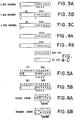
- two kbps slots are needed on the link 3 for each physical line, i.e. one data slot and one control slot.
- Each user has an offering of a two slot period at regular time intervals and the data slot when offered to the user is filled with the available data bits, the location of the delimiter bits 0..01 indicates the number of valid bits.
- FIG. 3-A, 3-B and 3-C represent the G-bit in the control slot and the data slot in cases of a 3-bit exchange, a 7-bit exchange and an 8- bit exchange. With such a structure, 32 users at 64 kbps or less use 64 slots at 64 kbps.
- Logical channels are based on 64-kbps digital slots multiplexed into external multiplex links connected to the LIC circuits.
- Figure 4-A shows the structure of the link slot in that case.
- Figure 4-B shows the data slot in case of a 56 kbps clear channel.
- 32 logical users at 56 kbps use 64 slots at 64 kbps.
- Figure 4-C shows the data and control slots in case of modem, terminal, network interfaces carried by 64 kbps slots.
- the same link offering is used to carry data or control information alternatively, i.e. every second slot relative to a given channel.
- the variable validation delimiter is used in the data slots, and the example shown in figure 4-C corresponds to valid entities of 6 bits.
- data and control slots have the same structure as in the general case in which two consecutive slots are used and the control slot identification is made through the G bit which is set at 1. With such a structure, 64 users at 24 kbps or less use 64 slots at 64 kbps (this includes the conventional 19.2 kb- ps users).
- the receive stream on the link 3-R looks as shown in figure 5-A wherein only the information required for the data transfers is represented.
- the transmit stream on link 3-T looks as shown in figure 5-B.
- G, V, and X have the same meaning as on the receive stream.
- the maximum number of valid bits to be transmitted (X-bits) is known by the line scanning means at the initialization time according to the type of users connected to the line interface circuits.
- the six remaining bits in the control slot are used for carrying the internal control information which can be continuously provided or specifically requested by the line scanning means 1 and external interface control information which must be exchanged with a higher rate than the internal control information, especially error and parity indications.
- control slot structures for the receive stream and for the transmit stream are shown in figures 6-A and 6-B respectively.
- the portion of the link bandwidth relative to this channel i.e. the ratio between the slots allocated to this channel and the total number of slots will be referred to as the link subchannel.
- the N-bit allows a modulo n framing mechanism.
- There is one N-bit per link subchannel, the N-bit being ON in one transmit control slot out of 8 allows to provide on the I-bit the address of an active tail gate 17 resource usually a register, to be read on the subsequent receive control slots relative to this channel.
- the address is provided at a rate of one bit per slot, similarly the contents of the addressed register is given at the rate of one bit per slot, the N-bit is also ON in one receive control slot out of 8.
- the 8 first values of the I-bit of the transmit control slot provide the address of an active tail gate 15 resource to be loaded, the 8 next values give the pattern to be loaded into that resource.
- 8 active tail gate 17 resources of 8 bits each can be permanently read/written at a rate of one bit per slot.
- the addresses of the 8 resources are supposed to be implicitly known.
- bit-N allows to present the modem-in or modem-out information i.e. 6 bits for V.24 interface on two control slots of a given link subchannel, 4 bits at a time placed on the E-bits.
- CRC cyclic redundancy code
- a CRC pattern can be carried on 16 slots of a given link subchannel, this CRC being calculated on 1 024 data bits.
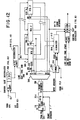
- Figure 7 represents the block diagram of the multiplexing circuit 5. It is connected to line scanning means 1 through interface multiplex transmit and receive links 3-T and 3-R carrying the link entities having the configurations described in reference to figures 3 to 6.
- the entities (control slots and data slots) relative to the users attached to line scanning means 1 constitutes a frame.
- a phase lock oscillator PLO 30 receives the bit stream to be transmitted from Xmit serial link 3-T and provides on line 9, a signal the frequency of which is twice the bit frequency on link 3-T, for example, it is assumed that the bit frequency is equal to 4.096 megahertz so that the PLO output signal has a 8.192 megahertz frequency. This is due to the fact that Manchester coded bits are processed by the line scanning means and that the Manchester code provides in one bit period the true bit value and its complement.
- a frame synchro detection circuit 32 generates the frame synchro signal on line 7 from the bit stream on link 3-T and from the output of the phase lock oscillator 30.
- the bit stream to be sent to line interface circuits 11 on line 13, from the transmit link 3-T is decoded in Manchester decoding circuit 34 and provided to line 13 through driver 36.
- switches SW1 and SW2 are close, since in that case the same synchro signal is used in the receive and the transmit parts of the line interface circuits. If the line scanning means is connected to a T1 multiplex line, these switches are open and switches SW3 and SW4 which were normally open are closed, and the line interface circuit provides a LIC PLO signal on line 9-R and a frame synchronization signal on line 7-R. This allows to have a perfect synchronism between the channels on the T1 line and the two-slots periods on the multiplex link 3. This will be explained later on in reference to figures 15 and 16.
- the bit stream is received from line interface circuits 11 through line 15 by receiver 38 and coded in Manchester encoding circuit 39 to be provided on link 3-R.
- Frame synchronization generating circuit 40 performs a Manchester code violation to send the frame synchro information to line scanning means 1 in order that the slots assigned to the plurality of users may be retrieved in line scanning means 1.
- switch SW1 When switch SW1 is closed frame synchronization generation circuit 40 receives the PLO output signal from PLO 30.
- switch SW1 is open and switches SW3 and 4 are closed, circuit 40 is actuated by the frame synchro receive signal on line 7-R and the LIC PLO output signal on line 9-R.
- Circuit 42 allows the wrap test of the link 3 to be made. This is done by connecting the transmit link to the receive link.
- Multiplexing circuit 5 comprises internal registers 44 in which line scanning means 1 may cause I- bits to be written through the write line WR at the output of decoding circuit 34. These I- bits are placed in control slots assigned to multiplexing circuit 5.
- registers 44 The content of registers 44 is read by line scanning means 1 though line RD connected at the input of encoding circuit 38.
- Registers 44 are shifted under control of the output signal from phase locked oscillator PLO 30 at the link clock rate which is derived from the phase locked oscillator 30 when switch SW2 is closed. When this switch is open in the case line scanning means 1 is connected to multiplex line (T1), the data in register 44 are written under control of PLO output signal on line 9 and are read under control of the LIC PLO output signal on line 9-R.
- This multiplexing circuit will not be described in more details since it has only for a function to make the interface between line interface circuits 11 and line scanning means 1, i.e. it receives the control and data slots from the line interface circuits and builds therefrom the succession of frames to be transmitted to line scanning means 1. Furthermore it causes the succession of frames to be sent through line 13 to the line interface circuit.
- each line interface circuit 11 The function of the receive part of each line interface circuit 11 is to generate from the bits received from the line users attached to it, entities having the configuration shown in figures 5-A and 6-A.
- Line interface address signals A0, A1 and A2 and a LIC type signal on line 51 are provided to slot decoder 50.
- the LIC type signal indicates that the line interface circuit is connected to four physical line users.
- Slot decoders has four output lines 52-1 to 52-4. The signal on each one of these output lines is active during the period including the data and control slots assigned to one user connected to the line interface circuit. For example, assuming that four users are connected to the line interface circuit, the signal on output line 52-1 is active during the period assigned to line 1 user, the signal on output line 52-2 is active during the period assigned to line 2 user, and so on...
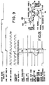
- Circuit 54 comprises flip flop circuit 56 activated by the signal from output line 9 from the multiplexing circuit, byte counter 58 and slot counter 60.
- Circuit 56 provides pulses at the bit clock frequency as shown in C in timing diagram of figure 9, from the PLO output signal shown in F.
- Byte counter 58 counts eight bit periods which correspond to the duration of a slot.
- the slots are counted by counter 60 which is reset by the frame synchro signal on line 7.
- there are 64 slots in a frame i. e. 32 data slots and 32 control slots.
- counter 60 counts up to 64.
- Output 62 of slot counter 60 is compared with the slot number decoded by decoder 50 in comparing circuit 64.
- Comparing circuit 64 has four outputs 66-1 to 66-4 which are active during the time periods (including the data and control slots) assigned on serial ink 3-R to the line users 1, 2, 3, 4 connected to the line interface circuit.
- the data are received from the modem by means of receiver 68, the modem clock receive signal (shown in A in figure 9) generated by the modem interface is provided through receiver 70 to the clock CK input of D-latch 72.
- the data in bits are provided through receiver 68 to the D-input of D-latch 72 acting as a one bit buffer.
- Contention logic 74 generates three clock signals shown in H, J and O in figure 9. These signals are derived from the line 1 slot time signal on line 66-1 which is active during the period assigned to line user 1 and from the modem receive clock B.
- This logic 74 is to synchronize the data bits received from the modem with the data slot time allocated to the line user to prevent a received bit from being lost. This is done by handling the contention between the modem clock receive and the data slot time allocated to the line in such a way that no data bit is lost.
- Shift register 76 is the data slot serializer. It is shifted by serializer clock D shown in figure 9, provided on shift input line 82. Serializer clock D is generated by gating circuit 84 from the link bit clock C and the line 1 slot time signal B. Gating circuit prevents the first bit clock pulse occurring at the beginning of the line slot time from being applied to the shift input of register 76. During this time, when clock 1 (H) is active at the output 86 of contention logic 74, the content of deserializer register 78 is loaded into serializer register 76 through bus 88.
- Deserializer register 78 is a 9-bit shift register in which the received data bits provided by one bit buffer latch 72 are inputted through input 92 under control of modem clock receive resynchro clock 3 (O) generated on output line 94 of contention logic 74. This clock 3 causes the data bit stored in latch 72 to be entered in register 78 and of the variable delimiter pattern to be shifted toward the right in register 78.
- serializer 76 The data bits in serializer 76 are shifted toward the right, under control of serializer clock D on line 82.
- bit 1 of the variable delimitation pattern would have been shifted in the right most position of register 78 to be used as the global validation bit in the control slot associated with the data slot.
- Modem control lines are associated to the modem data line.
- the control bits on these six lines are stored in registers 102 and 104 to be placed in the E-bits positions of the control slot (see figure 6-A). Since, only four E bits are available per control slot, two frames are used to send the six control bits, for example four bits are sent in the odd numbered frames and two bits are sent during the even numbered frames.
- Odd/even frame counter 106 which is controlled by the line 1 slot time signal on line 66-1 causes the content of the four control bits in register 102 to be loaded in control slot senalizer register 108 during the control slot time of a odd numbered frame and the two remaining control bits to be sent to the serializer register 108 during the control slot time of a even numbered frame.
- Control bits: G, TR, N and I are provided to control slot serializer 108 through register 110.
- G-bit is set in the left most position of register 110 to the value stored in the right most position R of register 78. Thus if the number of valid data bits in register 78 is lower than eight a 0 is stored in this position so that the G-bit in register 110 is set at 0.
- the left most bit (1) of the variable validation pattern is stored in the R position of register 78 and a 1 is stored as G-bit in register 110.
- the TR bit is set through line 114 from the transmit part of the line interface circuit.
- the I-bits are filled from line interface control internal registers 112. Assuming that there are eight 8- bit internal registers, 64 frames are required for placing the content of these registers, one bit at a time in the control slot assigned to the line user. The content of the internal registers is shifted in the I-position of register 110 under control of the line 1 slot time signal on line 66-1.
- Frame counter 115 counts the number of frames from the frame synchro signal on line 7, so as to cause the N-bit to be set to 0 every frame out of 64 through line 116. This allows the beginning and the end of the transmission of the internal register content to be determined.
- the internal registers are loaded though a scan/refresh mechanism which will be described in reference to figure 12.
- control of register 110 is loaded in control slot serializer shift register 108 under control of signal on slot line 1 time line 66-1 at the beginning of the time period assigned to the line, by means of clock 1 (H) signal on line 86.
- the data and control slot serializer registers 76 and 108 are serially connected and shifted under control of serializer clock signat (D) on line 82. This clock signal is inactive during the time, the registers are loaded.
- Output 118 which provides the serial control and data bits is gated to the line interface circuit output 15, to be sent to multiplexing circuit 5 through AND gate 120 which is conditioned by the signal on line 66-1.
- the outputs of the AND gates 120 of the receiving arrangements of each user connected to the plurality of line interface circuits are OR dotted so as to provide the data and control bits from the users connected to the line interface circuits in the assigned time periods to multiplexing circuit 5.
- the line interface circuit transmit part will now be described in reference to figures 10 and 11 which show the circuits required for sending the data and control bits from multiplexing circuit 5 to the users and the corresponding timing diagram. It uses the same line slot time signals as the receive part.
- Serializer shift register 200 providing the data bits to the user modem on line 202 through driver 204, during the time slot period assigned to the user, is to be loaded by the data bits coming from multiplexing circuit 5 on line 13.
- the data and control bits from multiplexing circuit 5 on line 13 are provided to data and control slot bit deserializer 206 at the bit clock rate (C in figure 9).
- a transmit clock pulse R (figure 14) is generated from the modem transmit clock P.
- This clock R is active during the next pulse provided by the phase lock oscillator following the leading edge of the modem transmit clock P. It is generated by single pulse generation circuit 208 which receives the modem transmit clock P through receiver 210 and the PLO output signal Q. Circuit 210 will be described in reference to figure 14.
- the data bits and the G bit in register 206 are loaded in data register 212.
- the load pulse is provided by AND gate 214 and is active at the slot time end when there is an active transmit request on line 114.
- the data register 212 content is loaded in 9-bit serializer 200 under control of load pulse U (figure 11) on line 232.
- serializer content is shifted to the right at the rate of Xmit pulse Q provided to the shift input through AND gate 216.
- Zeroes are inputted to replace the data bits shifted to the right, this is schematically represented in the figure by the 0 on input 218.
- comparator 220 compares the content of serializer 200 with the pattern 00000001 indicating that the data slot is empty. Assuming that the data slot has the configuration 0001 XXXX (four valid bits), G-bit is equal to 0. When bit 1 of the variable delimiter is located in the eight-th position of the serializer, comparator 220 detects an equality which means that the four data bits have been sent. If there is eight valid data bits in the data slot, G-bit is equal to 1, so that when G-bit is located in the eight-th position of the serializer, comparator 220 detects an equality which means that the eight data bits have been sent.
- the output signal S of comparator 220 on output line 222 is provided to the D-input of D-latch 224 which receives the PLO output signal (line 226) on its clock CK inputs.
- Latch 224 provides on its Q-output, comparator OUT delayed signal T.
- Signal T is provided at one input of AND gate 230 which receives on its second input, transmit pulse R from line 234.
- serializer 200 is loaded through active signal U.
- AND gate 230 is not conditioned and signal U is inactive.
- the transmit request bit TR is generated by D-latches 240 and 242.
- Latch 242 receives a 1 on its D-input and the load pulse from line 232 inverted in inverter 244. Thus it provides an UP active level on its Q-output on line 114 on the trailing edge of the load pulse (U in figure 11) on line 232, i.e. when data register 212 has been loaded in the serializer 200. Thus at that time the TR-bit is active.
- the clear request latch 240 is set on the next leading edge of the PLO pulses.
- the complemented output 0 of latch 240 is connected to the CLEAR input of D-latch 242 so that at that time latch 240 is reset and the TR-bit is at its inactive DOWN level.
- the transmit request TR bit is sent to the receive part of the line interface circuit.
- control bits in the control slot deserialized in deserializer register 206 are processed in the following way.
- the G and N bits are loaded in register 244.
- the N-bit is used for delimiting the I bit stream which is accumulated in a plurality of frames and loaded in 8-bit deserializer 246.
- the I bit of each control slot is provided at the input of deserializer 246, the content of which is shifted by the slot time end pulse on line 248.
- Deserializer register 246 feeds the internal control registers.
- the E external control bits are loaded in register 250 and 252.
- the first four bits are loaded in register 250 and the remaining two bits are loaded in register 252.
- the register loading control pulses on lines 258 and 260 are provided by AND gates 254 and 256 which receive on one of their inputs the slot time end from line 248 and on their second inputs the odd frame indication and the even frame indication respectively provided by counter 106 shown in the receive part (figure 8).
- register 250 is loaded during the odd numbered frame and register 252 is loaded during the even numbered frame.
- registers 250 and 252 are provided to the modem out control lines trough busses 262 and 264.
- registers 300-1 to 300-8 are loaded with the I-bits from the receive control part of deserializer 206 and 8-bits deserializer 246 through bus 302. The content of registers 300-1 to 300-8 is transferred in 8-bits serializer 112 and control slot serializer 108 of receive part of the line interface control circuit through bus 304.
- Frame counter 306 is connected to the output of byte counter 58 shown in figure 8. It counts the frames modulo 63. Decoder 308 generates from the output of counter 306 signals on its output lines 310 which are active during frames 0 to 63. For example signal on line 310-0 is active during frame 0 and signal on line 310-9 is active during frame 9.
- Line 310-0, line 310-7, line 310-15 ...to line 310-55 are connected to the read input of registers 300-1 to 300-8 respectively so as to cause the content of these registers to be sent on bus 304 when the signals on these output lines of decoder 308 are active.
- Line 310-7, line 310-15, line 310-23 ....to line 310-63 are connected to the write input of registers 300-1 to 300-8 so as to cause the content of deserializer 246 to be transferred in internal registers 300-1 to 300-8 when the signals on these output lines of decoder 308 are active.
- timing circuit causes a loading pulse to be provided on output line 314. This causes the content of one of the internal registers depending upon which read lines is active to be provided to serializer 112.
- each frame from frame 0 to frame 7 eight I-bits are accumulated in deserializer 246.
- write line 310-7 is active and the content of deserializer 246 is loaded into register 300-1.
- the same process occurs for frames 8 to 15, 16 to 23, 24 to 31, 32 to 39, 40 to 47, 48 to 55 and 56 to 63 for loading registers 300-2 to 300-8 when lines 310-15, 300-23, 300-31, 310-39, 310-47, 310-55, 310-63 are active.
- registers 300-1 to 300-8 are transferred to serializer 112 when lines 310-1, 310-7, 310-15, 310-23, 310-31, 310-39, 310-47 and 310-55 are active.
- the bit which is shifted out of the serializer 112 is placed in the I-bit position of control slot serializer 108 of the receive part of the line interface circuit to be sent to the multiplexing circuit.
- the N delimiting bit is set at 0 in deserializer 108, when frame 63 is decoded by decoder 308.
- a 1 is provided on D-input 406 of latch 400 and data slot time early signal K is provided on the CK input.
- Latch 400 is reset by data slot time delayed signal L.
- the complemented 0 output 408 of latch 400 is provided to one input of OR circuit 404.
- the other input of OR circuit 404 is connected to the Q-output 94 of latch 402.
- the CK-input of latch 402 is connected to the PLO output line 9 and its clear input is connected to the modem clock receive line at the output of receiver 70 (signal A in figure 9).
- the modem clock resynch signal goes UP at the next leading edge of the PLO pulse provided that the modem clock inhibit latch 400 is at its UP level.
- This modem clock inhibit latch 400 is used to delay the modem clock in the case of contention with the load serializer signal H.
- the modem clock inhibit latch complemented output n is set to its DOWN level at the leading edge of data slot time early signal K and set back to UP level by the data slot time delayed singal L.
- the data slot serializer 76 is loaded with deserializer 78 content and then the variable delimiter is loaded in the deserializer 78. Then the next data bit coming from the one bit buffer 72 can be shifted into the deserializer 78.
- Figure 14 represents the single pulse generating circuit 208 of figure 10. It generates the R transmit clock pulse from the modem transmit clock P and the PLO output signal Q. It comprises three D-latches 500,502 and 504, AND gates 506 and 508 and inverter 510.
- D-input of latch 500 receives the modem transmit clock signal P and its CK-input receives the PLO output signal Q.
- Output of latch 500 is connected to D-input of latch 502.
- CK-input of latch 500 receives the PLO output signal inverted by inverter 510.
- Output of latch 502 is connected to one input of AND gate 506. The other input of AND gate 506 is connected to the Q-output of latch 500.
- the output of AND gate 506 is connected to the CK-input of latch 504, the D-input of which is set to 1.
- the complemented 0 output of latch 504 is provided to one input of AND gate 508, the other input of which receives the modem transmit clock P signal.
- the clear inputs of latches 500 and 502 are connected to the output of AND gate 508 and the clear input of latch 504 receives the modem transmit clock P signal.
- the multiplexing circuit 5 is attached to one line interface circuit only and switches SW3 and SW4 are closed and switches SW1 and SW2 are open. This allows the frame synchro on link 3-R to be generated in synchronism with the frame synchro signal retrieved from the received data.
- the same frame synchro signal must be used in the transmit part on link 3-T and the T1 line and in the receive part on the T1 line and link 3-R.
- the bit clocks have to be inphase, the clock frequency on link 3 is twice the clock frequency on the T1 line since two eight-bit slots (data and control) correspond to one T1 channel (data or signalling).
- the G bit may be permanently coded in the control slot to 1 indicating that eight bits are valid in the data slot or this indication may be permanently provided to the line interface circuit and the G-bit position may be used for exchanging additional control information.
- T1 line controls the frame synchro generation and the bit clock signal in receive and the line scanning means controls the frame synchro generation and the bit clock signal in transmit.
- contention logic 74 shown in figure 8 is no more required in the receive part of the line interface circuit.
- Phase locked oscillator retrieves the clock signal on the T1 line at a frequency equal to 16-324 megahertz in the chosen example.
- the output of PLO 602 is provided to a frequency divider made of two flip-flop circuits 604 and 606.
- Phase locked oscillator 600 output line constitutes line 9-R which is provided to the multiplexing circuit 5.
- the output of flip-flop 604 provides the link bit clock on line 608 and the output of flip-flop 606 provides the T1 bit clock on line 610.
- Link bit clock frequency is twice the T1 bit clock i.e. 8.192 and 4.096 MHz respectively.
- T1 bit clock is provided to the shift input of deserializer 612 in which the received data bits are inputted by receiver 600.
- the content of deserializer 612 is provided to a synchro pattern detection circuit 615 through bus 616.
- Circuit 614 works under control of the T1 bit clock signal and generates on its output line 7-R the frame synchro receive signal which is provided to multiplexing circuit 5. This signal is active when circuit 614 recognizes in deserializer 612 the synchro pattern which is sent in the channel 0 of the T1 line.
- Byte counter 616 connected to flip-flop 618 generates a channel selection signal on line 620.
- Byte counter counts the link bit clock pulses from line 608. Each time the selection signal is active the content of deserializer 612 is loaded into link data slot deserializer 622.
- T1 channel counter 624 which provides active signals on output lines 626 and 628 when channel 1 and channel 16 are decoded. These channels are used for exchanging signalling information which is to be loaded in the E-bit position of the link control slots. Consequently, these signals are provided through OR gate 627 to gating circuit 630 which causes the content of deserializer 612 to be provided to control slot serializer 632 when the channel selection signal on line 620 is active.
- Byte counter 616 and channel counter 624 are reset by the frame synchro signal from line 7-R.
- Data slot serializer 622 and control slot serializer 632 are serially connected and shifted under control of the link bit clock signal on line 608, so as to provide the serial data and control bits to the multiplexing circuits 5 on link 15.
- the I and N bits are loaded in the control slot as described in reference to figure 8. This mechanism is schematically shown in box 634 and is inhibited through inverter 636 when the signals on line 626 and 628 are active.
- the transmit part of the T1 line interface circuit is shown in figure 16.
- control and data slot deserializer 700 which receives the serial data and control bits from transmit link 13 at the output of multiplexing circuit 5.
- the content of deserializer 700 is shifted under control of the PLO output signal on line 9 i.e. at a frequency of 8.192 MHz.
- the PLO output signal is provided to flip flop circuit which provides on its output line a signal at a frequency equal to 4.096 MHz which is applied on the shift input of serializer 706 so as to cause serializer 706 to be shifted at the T1 bit rate.
- the PLO output signal is also provided to byte counter 708, the output of which is applied to flip-flop 710 which provides on its output line a channel selection signal which is active to cause the content of the data slot in deserializer 700 to be loaded into serializer 706 through gating circuit 714.
- OR gate 718 The inputs of OR gate 718 are provided with the channel 1 and channel 16 indications from counter 716 and the inputs of NOR gate 720 are provided with the output of OR gate 718 and channel 0 indication from counter 716.
- gating circuit 714 is inhibited and gating circuit 724 is provided with an active gating signal which causes the content of the external control bits E in the control slot to be transferred into serializer 706.
- Gating circuit 714 When channel 0 is decoded, gating circuit 714 is inhibited so that the data slot content is not transferred to serializer 706. Gating circuit 726 causes the synchro pattern which is generated in frame synchro pattern generation circuit 728 under control of the frame transmit control signal on line 7 to be sent to serializer 706.
- serializer 706 The bits shifted out of serializer 706 are provided through driver 730 to the T1 link.
- I control bits are processed in the way described in reference to figure 12. This is schematically shown by logic 730. I-bits are provided to the internal control logic through gating circuit 732. The output of OR gate 718 is inverted in inverter 734. Thus, when channel 1 or channel 16 is decoded, the transfer of I-bits to logic 730 is inhibited.
Description
- This invention relates to a multiplex interface for the line scanners of a communication controller, allowing the communication controller to be connected to any type of physical or logical attachments.
- To day, the communication controller may be connected to physical attachments such as modems or network standard data interfaces such as V24, V35, Bell 303, X21 or any local attached interface working at any speed or to logical attachments such as Time Division Multiplex links (T1, CEPT (Conférence Europeenne des Postes et Telecommunications) first order mutliplex, Integrated Service Digital Network ISDN basic access, ISDN extended access) or to PBX interfaces.
- Patent Application EP-
A 0 077 863 describes a line adapter to be used in a communication controller. This line adapter presents one drawback. Since it has to be connected to a plurality of users through line connectors having a quite large size, the adapters are distant from each others and thus the bus-connecting them to the Central Control Unit is long which causes the transit delays on the bus to be long and the performances of the Communication Controller to be degraded. - Furthermore, such a line adapter cannot accommodate user lines at a speed higher than 256 kilobits per second.
- In the digital telephone exchange field, it is known from EP-
A 0 016 426 to allocate a channel at a given rate (64 Kbit/s) for the speech and one at an equal rate for the signalling to each subscriber which has access to the connection network. - An object of this invention is to provide the line scanners of the communication controller with a multiplex interface which allows the communication controller to be connected to any type of users.
- Another object of the invention is to provide such a multiplex interface which allows the performance of the communication controller to be improved.
- The multiplex interface according to the invention as set forth in
claim 1 is to be connected to the scanning means of a communication controller in order to exchange data and control bits between the line scanning means and the user attached to the communication controller. - The data and control bits are carried in data and control slots respectively, said slots having specific structures which give the communicating controller its versatility.
- The interface comprises transmit and receive synchronous multiplex links connecting the line scanning means to the users through multiplexing means, the data and control bits being exchanged on the transmit and receive multiplex links in synchronous frames wherein at least one data slot and one control slot are assigned to each user, the structures of the two slots being identical for all types of users.
- The data slot comprises n bits which include a variable number x of valid bits depending upon the line speed of the user information carrying medium (line or multiplex link) assigned to the data slot, said number being indicated by a variable delimitation pattern comprising a first delimiting bit set at a first binary value (1) adjacent to the data bits and (n-x-1) bits set at the second binary value (0) adjacent to said first delimiting bit.
- The control slot also comprises n bits, wherein a first bit is used as global validation bit in case the data slot comprises n valid bits (x=n), this bit being set at the first binary value (1) when the data slot comprises n valid bits and at the second binary value (0) if it comprises less than n valid bits, and the n-1 other bits being used for exchanging control information.
-
- Figure 1 shows schematically a communication controller wherein the present invention may be embodied.
- Figure 2 shows the block diagram of the line adapter incorporating the multiplex interface according to the present invention.
- Figures 3A-3C represent the link entities in cases of a 3-valid bit exchange, a 7-valid bit exchange and an 8-valid bit exchange.
- Figure 4-A and 4-b show the link entities in case of an 8-bit exchange and a 7-bit exchange for a logical 64 kbps user and a 56 kbps user, and figure 4-C shows the data and control slots in case of low speed users.
- Figure 5-A and 5-B show the receive stream and the transmit stream respectively with only the control information required for the data transfer.
- Figure 6-A and 6-B show the control slots for the receive stream and the transmit stream respectively.
- Figure 7 shows the block diagram of the multiplexing circuit.
- Figure 8 shows the receive part of the line interface circuit.
- Figure 9 shows the timing diagram of the receive part of line interface circuit shown in figure 8.
- Figure 10 shows the transmit part of the line interface circuit
- Figure 11 shows the timing diagram of the transmit part of the line interface circuit.
- Figure 12 shows the scan and refresh circuit used for arranging the bits to be exchanged in the control slots.
- Figure 13 shows the modem clock resynchro signal generating circuit of the receive part of the line interface circuit.
- Figure 14 shows the single
pulse generating circuit 208 of the transmit part of the line interface circuit. - Figure 15 shows the receive part of the line interface circuit to be used for connecting the line scanning means to a multiplex user link.
- Figure 16 shows the transmit part of the line interface circuit to be used for connecting the line scanning means to a multiplex user link.
- As described in European Patent Application 81 430 037.2 filed on October 28, 1981 and published under
number 0 077 863, a communication controller comprises as schematically represented in figure 1, a central control unit CCU connected on the one hand to communication lines through line adapters and on the other hand to central processing units through channel adapters. The line adapters serve at least one user line by means of a cyclic scanning device and a random access memory assembly containing the data received or to be sent on the various lines as controlled by the scanning device. - The line adapter according to the present invention is schematically shown in figure 2. It is comprised of line scanning means 1 which are similar to the line scanning means such as described in above patent application except that a
full duplex link 3 is provided at the output of the line scanning means. A slot or a plurality of slots, is assigned to each user connected to the adapter so that the data and control bits from/to the line users are exchanged in said slots on synchronous links 3R and 3T. The succession of slots assigned to the users attached to an adapter constitutes a frame. -
Link 3 is connected tomultiplexing device 5 which generates from the bits received from line scanning means 1, a frame synchronization signal online 7 and a bit clock signal ofline 9 and transmits the data and control bits from the transmit link 3-T to lineinterface circuits LIC 11 throughline 13. It is assumed that there are eight LIC circuits numbered 11-1 to 11-8. This allows to attach from one line at up to 2 megabits per second to thirty two physical or logical channels at up to 64 kilobits per second. - The bits received from the users through
line interface circuits 11 are transmitted tomultiplexing circuit 5 which provides them through receive link 3-R, to line scanning means 1. - Thanks to the provision of the
serial link 3,line interface circuits 11 may be apart from the communication controller in a separate active tail gate enclosure 17. Thus the transit delay on the bus connecting the adapters to the CCU is reduced in a significant way, since the bus length is reduced due to the fact that the line adapters may be close together since there is only one connection to thelink 3. - According to the present invention, elementary entities called link offerings or link slots allow several types of information (data and control) to be carried. The structure of these entities which is shown in figures 3 to 6 is determined in such a way that they can be used easily in terms of cost and efficiently in terms of thruput by the various types of attachments. For a given attachment, the line interface circuit is in charge of transforming the link entities into information fitting this particular attachment interface, and vice-versa. The amount of transformation functions must be minimum. The structure of the entities is driven by cost and performance machine requirements rather than external considerations, such as an optimized link bandwidth or a compatibility with a standardized link structure.
- The link must carry three types of information:
- Data and service bits
- External interface control (In and Out)
- LIC/Multiplex internal control
- For exchanging data and service bits a basic principle is to let
LIC circuits 11 be responsible for bit clocking.. This service information is either derived from dock signals provided by the attachments or in- temally generated by theLIC circuits 11. This allows the line scanning means to be relieved from the handling of the various clocking types of the low-speed attachments. - The valid data bits between active tail gate 17 and line scanning means 1 could be exchanged in different ways according to the known techniques, as described hereafter.
- Valid data bits may be placed into blocks, delimited by some types of flags. This approach is used in the so called Digital Multiplex Interface DMI proposed by A. T. T. (Described in Digital Multiplex Interface Specification AT & T Information Systems, March 5, 1984) the blocks being similar to HDLC frames. This would allow a large variety of attachment speeds to be accommodated but would have a serious cost drawback at both active tail gate and line scanning means sides in terms of buffering capability and block handling.
- Data may be individually be validated by service bits: Receive service RS and transmit request TR bits may be generated by LIC circuits. This would lead to the following structure for each link offering: inbound active tail gate to scanning means R RS TR outbound scanning means to active tail gate T
- R is the receive data bit and T is the transmit data bit.
- RS=1 means that the present R-bit is valid and must be taken by the line scanning means.
- RS=0 means that the present link offering does not carry any valid data bit.
- TR=1 means that a new data bit is requested by the active tail gate. The T data bit of the next offerings relative to this channel will contain a valid transmit data bit. The line scanning means must serve the bit requested by the active tail gate before the next active tail gate request to avoid underrun conditions. The active tail gate can thus systematically takes the transmit bit into account each time it requests a new bit, thus eliminating the need to validate the T-bit.
- TR=0 means that the active tail gate does not request any data bit.
- Such an offering scheme based on the transfer of single bits, would introduce a ratio of 3 between offering bits R, TR, RS and valid data bits. This is not acceptable for high speed attachments, as this implies a too high data rate on the link.
- A byte offering structure would require less overhead, but it would be necessary to indicate how many data bits are valid in this present offering, from 0 to 5. This would systematically waste 3 bits out of 8 and limit the maximum usable speed to 40 kbps for an offering speed of 64 kpbs.
- According to the Computer to PBX Interface CPI specifications, developed by Digital Equipment Corp DEC and Northern Telecom Inc NT, and described in PBX Systems proposal for an enhanced, γ-low Interface for the transmission of data (CPI), Digital Equipment Corp. (DEC) Northern Telecom Inc. (NT) March 1984 data bits could be buffered until a predetermined number of them forming a character are ready to be carried in a link offering at 64 kbps. This means that it is necessary to distinguish between empty and valid bit slots by using one bit per offering for that purpose. Thus the maximum allowable speed is limited to 56 kbps and data buffering is needed for each channel. Furthermore, this kind of data transfer suffers important delay distortions.
- To overcome this drawback, the present invention makes use of a dynamic variable data delimitation pattern which allows data bits to be transferred in each link offering in the following way:

- The
configuration 0..01 preceding the valid data bits is called the variable delimitation pattern or variable delimiter. Thus, the line scanning means knows the number of valid data bits received in one link offering in the following way. The first bit (position 0) is analyzed. If it is found at 1, the following bits are taken as valid data bits. If it is found at 0, the following bit (position 2) is analyzed. If it is found at 1, the following bits are taken as valid data bits if not the following bit (position 3) is analyzed, and so on... A data delimiter having theinverted configuration 1.. 10 has the same property. - For 8 valid bits, a global validation bit is needed as will be described later on.
- For physical channels at up to 64 kpbs, two kbps slots are needed on the
link 3 for each physical line, i.e. one data slot and one control slot. Each user has an offering of a two slot period at regular time intervals and the data slot when offered to the user is filled with the available data bits, the location of thedelimiter bits 0..01 indicates the number of valid bits. - Most of the bits in the control slot will be described later on, but one bit called the global validation bit or G bit indicates whether the whole data slot is valid (G=1) or not (G=0). Figures 3-A, 3-B and 3-C represent the G-bit in the control slot and the data slot in cases of a 3-bit exchange, a 7-bit exchange and an 8- bit exchange. With such a structure, 32 users at 64 kbps or
less use 64 slots at 64 kbps. - Logical channels are based on 64-kbps digital slots multiplexed into external multiplex links connected to the LIC circuits.
- In case of a 64 kbps clear channel, no extemal control information must be carried on a channel basis. Figure 4-A shows the structure of the link slot in that case. The global validation bit G=1 is permanently provided in the control slot which may also be used for exchanging internal control information or diagnostic information. This information is coded as will be described in reference to figure 6-A and 6-B.
- It is to be noted that data are exchanged by bytes on both the external multiplex links and
link 3. - Figure 4-B shows the data slot in case of a 56 kbps clear channel. The global validation bit G=0 is permanently provided in the control slot and there are 7 valid bits in the data slot. With such a
structure 32 logical users at 56 kbps use 64 slots at 64 kbps. - Figure 4-C shows the data and control slots in case of modem, terminal, network interfaces carried by 64 kbps slots. For such low speed attachments, up to 24 kbps, the same link offering is used to carry data or control information alternatively, i.e. every second slot relative to a given channel. The first bit in the slot distinguishes between data (first bit=0) and control (first bit=1). The variable validation delimiter is used in the data slots, and the example shown in figure 4-C corresponds to valid entities of 6 bits. This shows that data and control slots have the same structure as in the general case in which two consecutive slots are used and the control slot identification is made through the G bit which is set at 1. With such a structure, 64 users at 24 kbps or
less use 64 slots at 64 kbps (this includes the conventional 19.2 kb- ps users). - For each channel, the receive stream on the link 3-R looks as shown in figure 5-A wherein only the information required for the data transfers is represented.
- G is the global validation bit
- G=0 see variable validation delimiter in the data slot
-
G =1 8 bits of the data slot are valid
- TR (Transmit Request) is set by the active tail gate 17 transmit leg to request a new data slot.
- TR=1: transmit data slot requested
- TR=O: no request
- V-bits constitute the variable delimiter
- X-bits are the valid data bits
- For each channel, the transmit stream on link 3-T looks as shown in figure 5-B. G, V, and X have the same meaning as on the receive stream. The maximum number of valid bits to be transmitted (X-bits) is known by the line scanning means at the initialization time according to the type of users connected to the line interface circuits.
- The six remaining bits in the control slot are used for carrying the internal control information which can be continuously provided or specifically requested by the line scanning means 1 and external interface control information which must be exchanged with a higher rate than the internal control information, especially error and parity indications.
- The control slot structures for the receive stream and for the transmit stream are shown in figures 6-A and 6-B respectively.
- Bit N is used for the control slot numbering.
- I is used as an internal control bit
- E are used as external control bits.
- Once one or several link offerings have been allocated to a given physical or logical channel, the portion of the link bandwidth relative to this channel, i.e. the ratio between the slots allocated to this channel and the total number of slots will be referred to as the link subchannel.
- The N-bit allows a modulo n framing mechanism. There is one N-bit per link subchannel, the N-bit being ON in one transmit control slot out of 8 allows to provide on the I-bit the address of an active tail gate 17 resource usually a register, to be read on the subsequent receive control slots relative to this channel. In this case, the address is provided at a rate of one bit per slot, similarly the contents of the addressed register is given at the rate of one bit per slot, the N-bit is also ON in one receive control slot out of 8.
- Similarly, if the N-bit is ON in one transmit control slot out of 16, the 8 first values of the I-bit of the transmit control slot provide the address of an
active tail gate 15 resource to be loaded, the 8 next values give the pattern to be loaded into that resource. - Similarly, if this bit is ON in one receive/transmit control slot out of 64, 8 active tail gate 17 resources of 8 bits each can be permanently read/written at a rate of one bit per slot. The addresses of the 8 resources are supposed to be implicitly known.
- When users are connected to the line interface circuits through modems, bit-N allows to present the modem-in or modem-out information i.e. 6 bits for V.24 interface on two control slots of a given link subchannel, 4 bits at a time placed on the E-bits.
- Similarly, as far as error isolation is concerned, the N-bit can indicate that the I-bit carries a parity bit or a bit of a CRC pattern (CRC= cyclic redundancy code), calculated on data and/or control bits.
- As an example, a CRC pattern can be carried on 16 slots of a given link subchannel, this CRC being calculated on 1 024 data bits.
- Figure 7 represents the block diagram of the
multiplexing circuit 5. It is connected to line scanning means 1 through interface multiplex transmit and receive links 3-T and 3-R carrying the link entities having the configurations described in reference to figures 3 to 6. The entities (control slots and data slots) relative to the users attached to line scanning means 1 constitutes a frame. A phaselock oscillator PLO 30 receives the bit stream to be transmitted from Xmit serial link 3-T and provides online 9, a signal the frequency of which is twice the bit frequency on link 3-T, for example, it is assumed that the bit frequency is equal to 4.096 megahertz so that the PLO output signal has a 8.192 megahertz frequency. This is due to the fact that Manchester coded bits are processed by the line scanning means and that the Manchester code provides in one bit period the true bit value and its complement. - A frame
synchro detection circuit 32 generates the frame synchro signal online 7 from the bit stream on link 3-T and from the output of thephase lock oscillator 30. The bit stream to be sent toline interface circuits 11 online 13, from the transmit link 3-T is decoded inManchester decoding circuit 34 and provided toline 13 throughdriver 36. - When the line scanning means is connected to physical or logical user lines except a multiplex line of the T1 type for example, switches SW1 and SW2 are close, since in that case the same synchro signal is used in the receive and the transmit parts of the line interface circuits. If the line scanning means is connected to a T1 multiplex line, these switches are open and switches SW3 and SW4 which were normally open are closed, and the line interface circuit provides a LIC PLO signal on line 9-R and a frame synchronization signal on line 7-R. This allows to have a perfect synchronism between the channels on the T1 line and the two-slots periods on the
multiplex link 3. This will be explained later on in reference to figures 15 and 16. - The bit stream is received from
line interface circuits 11 throughline 15 byreceiver 38 and coded inManchester encoding circuit 39 to be provided on link 3-R. Framesynchronization generating circuit 40 performs a Manchester code violation to send the frame synchro information to line scanning means 1 in order that the slots assigned to the plurality of users may be retrieved in line scanning means 1. When switch SW1 is closed framesynchronization generation circuit 40 receives the PLO output signal fromPLO 30. When switch SW1 is open and switches SW3 and 4 are closed,circuit 40 is actuated by the frame synchro receive signal on line 7-R and the LIC PLO output signal on line 9-R. Circuit 42 allows the wrap test of thelink 3 to be made. This is done by connecting the transmit link to the receive link. - Multiplexing
circuit 5 comprisesinternal registers 44 in which line scanning means 1 may cause I- bits to be written through the write line WR at the output ofdecoding circuit 34. These I- bits are placed in control slots assigned to multiplexingcircuit 5. - The content of
registers 44 is read by line scanning means 1 though line RD connected at the input of encodingcircuit 38. -
Registers 44 are shifted under control of the output signal from phase lockedoscillator PLO 30 at the link clock rate which is derived from the phase lockedoscillator 30 when switch SW2 is closed. When this switch is open in the case line scanning means 1 is connected to multiplex line (T1), the data inregister 44 are written under control of PLO output signal online 9 and are read under control of the LIC PLO output signal on line 9-R. - This multiplexing circuit will not be described in more details since it has only for a function to make the interface between
line interface circuits 11 and line scanning means 1, i.e. it receives the control and data slots from the line interface circuits and builds therefrom the succession of frames to be transmitted to line scanning means 1. Furthermore it causes the succession of frames to be sent throughline 13 to the line interface circuit. - It will now be described in reference to figure 8, the receive part of a line interface circuit which is connected to physical users through a modem. In the line interface circuits connected to logical users, the data input means are different and another type of line interface circuit will be described later on.
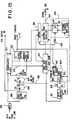
- The function of the receive part of each
line interface circuit 11 is to generate from the bits received from the line users attached to it, entities having the configuration shown in figures 5-A and 6-A. - Line interface address signals A0, A1 and A2 and a LIC type signal on
line 51 are provided to slotdecoder 50. In figure 8 it is assumed that the LIC type signal indicates that the line interface circuit is connected to four physical line users. Slot decoders has four output lines 52-1 to 52-4. The signal on each one of these output lines is active during the period including the data and control slots assigned to one user connected to the line interface circuit. For example, assuming that four users are connected to the line interface circuit, the signal on output line 52-1 is active during the period assigned toline 1 user, the signal on output line 52-2 is active during the period assigned toline 2 user, and so on... -
Circuit 54 comprisesflip flop circuit 56 activated by the signal fromoutput line 9 from the multiplexing circuit,byte counter 58 andslot counter 60.Circuit 56 provides pulses at the bit clock frequency as shown in C in timing diagram of figure 9, from the PLO output signal shown in F. Byte counter 58 counts eight bit periods which correspond to the duration of a slot. The slots are counted by counter 60 which is reset by the frame synchro signal online 7. In the case where there are eight line interface circuits 11-1 to 11-8 and where each line interface circuit may be connected to four users, there are 64 slots in a frame, i. e. 32 data slots and 32 control slots. Thus counter 60 counts up to 64. - Output 62 of
slot counter 60 is compared with the slot number decoded bydecoder 50 in comparingcircuit 64. Comparingcircuit 64 has four outputs 66-1 to 66-4 which are active during the time periods (including the data and control slots) assigned on serial ink 3-R to theline users - The data are received from the modem by means of
receiver 68, the modem clock receive signal (shown in A in figure 9) generated by the modem interface is provided throughreceiver 70 to the clock CK input of D-latch 72. The data in bits are provided throughreceiver 68 to the D-input of D-latch 72 acting as a one bit buffer. -
Contention logic 74 generates three clock signals shown in H, J and O in figure 9. These signals are derived from theline 1 slot time signal on line 66-1 which is active during the period assigned toline user 1 and from the modem receive clock B. - The purpose of this
logic 74 is to synchronize the data bits received from the modem with the data slot time allocated to the line user to prevent a received bit from being lost. This is done by handling the contention between the modem clock receive and the data slot time allocated to the line in such a way that no data bit is lost. - Three
registers Shift register 76 is the data slot serializer. It is shifted by serializer clock D shown in figure 9, provided onshift input line 82. Serializer clock D is generated by gatingcircuit 84 from the link bit clock C and theline 1 slot time signal B. Gating circuit prevents the first bit clock pulse occurring at the beginning of the line slot time from being applied to the shift input ofregister 76. During this time, when clock 1 (H) is active at theoutput 86 ofcontention logic 74, the content ofdeserializer register 78 is loaded intoserializer register 76 throughbus 88. - Then when clock 2 (J) is active on
output line 90 ofcontention logic 74, the variable validation pattern 100000000 stored inregister 80 is loaded indeserializer register 78.Deserializer register 78 is a 9-bit shift register in which the received data bits provided by onebit buffer latch 72 are inputted throughinput 92 under control of modem clock receive resynchro clock 3 (O) generated onoutput line 94 ofcontention logic 74. Thisclock 3 causes the data bit stored inlatch 72 to be entered inregister 78 and of the variable delimiter pattern to be shifted toward the right inregister 78. - Thus when the line slot time signal becomes UP, the three following steps are performed:
- -
loading deserializer 78 intoserializer 76 - -loading the variable data delimiter into
deserializer 76 - -entering a new bit (if any) from modem into the data deserializer using the
resynchronized modem clock 3, - At that time the three steps described above are resumed.
- The data bits in
serializer 76 are shifted toward the right, under control of serializer clock D online 82. - If there were eight valid data bits in
register 78, thebit 1 of the variable delimitation pattern would have been shifted in the right most position ofregister 78 to be used as the global validation bit in the control slot associated with the data slot. - It will now be described how the control slot is built.
- Modem control lines are associated to the modem data line. There are usually six control lines schematically represented as
bus 100. The control bits on these six lines are stored inregisters - Odd/even
frame counter 106 which is controlled by theline 1 slot time signal on line 66-1 causes the content of the four control bits inregister 102 to be loaded in controlslot senalizer register 108 during the control slot time of a odd numbered frame and the two remaining control bits to be sent to theserializer register 108 during the control slot time of a even numbered frame. - Control bits: G, TR, N and I are provided to control
slot serializer 108 throughregister 110. G-bit is set in the left most position ofregister 110 to the value stored in the right most position R ofregister 78. Thus if the number of valid data bits inregister 78 is lower than eight a 0 is stored in this position so that the G-bit inregister 110 is set at 0. - If there are eight valid data bits in
deserializer register 78, the left most bit (1) of the variable validation pattern is stored in the R position ofregister 78 and a 1 is stored as G-bit inregister 110. - The TR bit is set through
line 114 from the transmit part of the line interface circuit. - The I-bits are filled from line interface control
internal registers 112. Assuming that there are eight 8- bit internal registers, 64 frames are required for placing the content of these registers, one bit at a time in the control slot assigned to the line user. The content of the internal registers is shifted in the I-position ofregister 110 under control of theline 1 slot time signal on line 66-1. -
Frame counter 115 counts the number of frames from the frame synchro signal online 7, so as to cause the N-bit to be set to 0 every frame out of 64 through line 116. This allows the beginning and the end of the transmission of the internal register content to be determined. - The internal registers are loaded though a scan/refresh mechanism which will be described in reference to figure 12.
- The control of
register 110 is loaded in control slotserializer shift register 108 under control of signal onslot line 1 time line 66-1 at the beginning of the time period assigned to the line, by means of clock 1 (H) signal online 86. - The data and control slot serializer registers 76 and 108 are serially connected and shifted under control of serializer clock signat (D) on
line 82. This clock signal is inactive during the time, the registers are loaded. -
Output 118 which provides the serial control and data bits is gated to the lineinterface circuit output 15, to be sent to multiplexingcircuit 5 through ANDgate 120 which is conditioned by the signal on line 66-1. - In the line interface circuit, similar arrangements are provided for each input line users.
Only circuits - The outputs of the AND
gates 120 of the receiving arrangements of each user connected to the plurality of line interface circuits are OR dotted so as to provide the data and control bits from the users connected to the line interface circuits in the assigned time periods to multiplexingcircuit 5. - The line interface circuit transmit part will now be described in reference to figures 10 and 11 which show the circuits required for sending the data and control bits from multiplexing
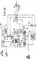
circuit 5 to the users and the corresponding timing diagram. It uses the same line slot time signals as the receive part. - Serializer shift register 200 providing the data bits to the user modem on
line 202 throughdriver 204, during the time slot period assigned to the user, is to be loaded by the data bits coming from multiplexingcircuit 5 online 13. The data and control bits from multiplexingcircuit 5 online 13 are provided to data and control slot bit deserializer 206 at the bit clock rate (C in figure 9). - As shown in figure 11, a transmit clock pulse R (figure 14) is generated from the modem transmit clock P. This clock R is active during the next pulse provided by the phase lock oscillator following the leading edge of the modem transmit clock P. It is generated by single
pulse generation circuit 208 which receives the modem transmit clock P throughreceiver 210 and the PLO outputsignal Q. Circuit 210 will be described in reference to figure 14. - At the line slot time signal end, the data bits and the G bit in
register 206 are loaded in data register 212. The load pulse is provided by ANDgate 214 and is active at the slot time end when there is an active transmit request online 114. - The data register 212 content is loaded in 9-bit serializer 200 under control of load pulse U (figure 11) on line 232.
- Once loaded, the serializer content is shifted to the right at the rate of Xmit pulse Q provided to the shift input through AND
gate 216. Zeroes are inputted to replace the data bits shifted to the right, this is schematically represented in the figure by the 0 on input 218. - To signal that the last bit has been sent,
comparator 220 compares the content of serializer 200 with the pattern 00000001 indicating that the data slot is empty. Assuming that the data slot has the configuration 0001 XXXX (four valid bits), G-bit is equal to 0. Whenbit 1 of the variable delimiter is located in the eight-th position of the serializer,comparator 220 detects an equality which means that the four data bits have been sent. If there is eight valid data bits in the data slot, G-bit is equal to 1, so that when G-bit is located in the eight-th position of the serializer,comparator 220 detects an equality which means that the eight data bits have been sent. - The output signal S of
comparator 220 onoutput line 222 is provided to the D-input of D-latch 224 which receives the PLO output signal (line 226) on its clock CK inputs. -
Latch 224 provides on its Q-output, comparator OUT delayed signal T. Signal T is provided at one input of ANDgate 230 which receives on its second input, transmit pulse R fromline 234. Thus when the valid data bits have been sent, serializer 200 is loaded through active signal U. - When no equality is detected, AND
gate 230 is not conditioned and signal U is inactive. - The Q-output of
latch 224 is inverted ininverter 236, thus ANDgate 216 is conditioned and transmit pulse signal R is provided to the shift input of serializer 200. - The transmit request bit TR is generated by D-
latches Latch 242 receives a 1 on its D-input and the load pulse from line 232 inverted ininverter 244. Thus it provides an UP active level on its Q-output online 114 on the trailing edge of the load pulse (U in figure 11) on line 232, i.e. when data register 212 has been loaded in the serializer 200. Thus at that time the TR-bit is active. - At the next slot time end detected by AND
gate 214, when the load data register pulse W becomes at an UP level, theclear request latch 240 is set on the next leading edge of the PLO pulses. The complementedoutput 0 oflatch 240 is connected to the CLEAR input of D-latch 242 so that at thattime latch 240 is reset and the TR-bit is at its inactive DOWN level. - The transmit request TR bit is sent to the receive part of the line interface circuit.
- The control bits in the control slot deserialized in
deserializer register 206 are processed in the following way. - At the slot time end, i.e. when the control and data bits relative to the line user are assembled in
register 206, the G and N bits are loaded inregister 244. The N-bit is used for delimiting the I bit stream which is accumulated in a plurality of frames and loaded in 8-bit deserializer 246. - The I bit of each control slot is provided at the input of
deserializer 246, the content of which is shifted by the slot time end pulse online 248. Deserializer register 246 feeds the internal control registers. - The E external control bits are loaded in
register register 250 and the remaining two bits are loaded inregister 252. The register loading control pulses onlines gates line 248 and on their second inputs the odd frame indication and the even frame indication respectively provided bycounter 106 shown in the receive part (figure 8). Thus register 250 is loaded during the odd numbered frame and register 252 is loaded during the even numbered frame. - The content of
registers - The scan/refresh mechanism will now be described in reference to figure 12.
- It is assumed that eight 8-bits internal registers are provided in the line interface circuit per user. Only one I bit relative to one user is provided to this assembly of registers per frame, thus 64 frames are needed to complete the loading of these registers with the I-bits relative to the user.
- Internal registers 300-1 to 300-8 are loaded with the I-bits from the receive control part of
deserializer 206 and 8-bits deserializer 246 throughbus 302. The content of registers 300-1 to 300-8 is transferred in 8-bits serializer 112 andcontrol slot serializer 108 of receive part of the line interface control circuit throughbus 304. -
Frame counter 306 is connected to the output ofbyte counter 58 shown in figure 8. It counts the frames modulo 63.Decoder 308 generates from the output ofcounter 306 signals on itsoutput lines 310 which are active duringframes 0 to 63. For example signal on line 310-0 is active duringframe 0 and signal on line 310-9 is active duringframe 9. - Line 310-0, line 310-7, line 310-15 ...to line 310-55 are connected to the read input of registers 300-1 to 300-8 respectively so as to cause the content of these registers to be sent on
bus 304 when the signals on these output lines ofdecoder 308 are active. - Line 310-7, line 310-15, line 310-23 ....to line 310-63 are connected to the write input of registers 300-1 to 300-8 so as to cause the content of
deserializer 246 to be transferred in internal registers 300-1 to 300-8 when the signals on these output lines ofdecoder 308 are active. - Each time eight bits are counted by
byte counter 58, timing circuit causes a loading pulse to be provided onoutput line 314. This causes the content of one of the internal registers depending upon which read lines is active to be provided toserializer 112. - During each frame from
frame 0 toframe 7, eight I-bits are accumulated indeserializer 246. Whenframe 7 is decoded, write line 310-7 is active and the content ofdeserializer 246 is loaded into register 300-1. The same process occurs forframes 8 to 15, 16 to 23, 24 to 31, 32 to 39, 40 to 47, 48 to 55 and 56 to 63 for loading registers 300-2 to 300-8 when lines 310-15, 300-23, 300-31, 310-39, 310-47, 310-55, 310-63 are active. - The content of these registers 300-1 to 300-8 are transferred to serializer 112 when lines 310-1, 310-7, 310-15, 310-23, 310-31, 310-39, 310-47 and 310-55 are active.
- Then as described in reference to figure 8, the bit which is shifted out of the
serializer 112 is placed in the I-bit position ofcontrol slot serializer 108 of the receive part of the line interface circuit to be sent to the multiplexing circuit. - The N delimiting bit is set at 0 in
deserializer 108, whenframe 63 is decoded bydecoder 308. - The circuit which allows the modem clock resynchro signal O in figure 9 to be generated is described in reference to figure 13.
- It comprises two D-
latches circuit 404. A 1 is provided on D-input 406 oflatch 400 and data slot time early signal K is provided on the CK input.Latch 400 is reset by data slot time delayed signal L. The complemented 0output 408 oflatch 400 is provided to one input of ORcircuit 404. The other input of ORcircuit 404 is connected to the Q-output 94 oflatch 402. The CK-input oflatch 402 is connected to thePLO output line 9 and its clear input is connected to the modem clock receive line at the output of receiver 70 (signal A in figure 9). - When the modem clock receive signal becomes at its UP level, the modem clock resynch signal goes UP at the next leading edge of the PLO pulse provided that the modem clock inhibit
latch 400 is at its UP level. This modem clock inhibitlatch 400 is used to delay the modem clock in the case of contention with the load serializer signal H. In this case the modem clock inhibit latch complemented output n is set to its DOWN level at the leading edge of data slot time early signal K and set back to UP level by the data slot time delayed singal L. During the time the modem clock inhibitlatch 400 complemented output is at DOWN level, thedata slot serializer 76 is loaded withdeserializer 78 content and then the variable delimiter is loaded in thedeserializer 78. Then the next data bit coming from the onebit buffer 72 can be shifted into thedeserializer 78. - Figure 14 represents the single
pulse generating circuit 208 of figure 10. It generates the R transmit clock pulse from the modem transmit clock P and the PLO output signal Q. It comprises three D-latches 500,502 and 504, ANDgates inverter 510. - D-input of
latch 500 receives the modem transmit clock signal P and its CK-input receives the PLO output signal Q. Output oflatch 500 is connected to D-input oflatch 502. CK-input oflatch 500 receives the PLO output signal inverted byinverter 510. Output oflatch 502 is connected to one input of ANDgate 506. The other input of ANDgate 506 is connected to the Q-output oflatch 500. - The output of AND
gate 506 is connected to the CK-input oflatch 504, the D-input of which is set to 1. The complemented 0 output oflatch 504 is provided to one input of ANDgate 508, the other input of which receives the modem transmit clock P signal. The clear inputs oflatches gate 508 and the clear input oflatch 504 receives the modem transmit clock P signal. - This arrangement allows one pulse from the PLO pulse stream to be provided on
output line 234 taken at the output oflatch 500 when the modem transmit clock signal is UP. This pulse which is provided to ANDgate 506 prevents the following pulses from the PLO from being provided onoutput 234. Thus signal R is generated onoutput line 234. - It will now be described in reference to figures 15 and 16 the receive and transmit part of the line interface circuit which is used for attaching the line scanning means to a digital multiplex line at 2.048 megabits per second such as a T1 line using the CEPT framing.
- In that case, the
multiplexing circuit 5 is attached to one line interface circuit only and switches SW3 and SW4 are closed and switches SW1 and SW2 are open. This allows the frame synchro on link 3-R to be generated in synchronism with the frame synchro signal retrieved from the received data. To insure a . perfect synchronism between the T1 channels and the two-slot periods on themultiplex link 3, the same frame synchro signal must be used in the transmit part on link 3-T and the T1 line and in the receive part on the T1 line and link 3-R. The bit clocks have to be inphase, the clock frequency onlink 3 is twice the clock frequency on the T1 line since two eight-bit slots (data and control) correspond to one T1 channel (data or signalling). It is no more required to use the global validation bit in the control slot since there are always eight bits to be sent or received in each data slot. Consequently the G bit may be permanently coded in the control slot to 1 indicating that eight bits are valid in the data slot or this indication may be permanently provided to the line interface circuit and the G-bit position may be used for exchanging additional control information. - Thus the T1 line controls the frame synchro generation and the bit clock signal in receive and the line scanning means controls the frame synchro generation and the bit clock signal in transmit.
- Consequently, the
contention logic 74 shown in figure 8 is no more required in the receive part of the line interface circuit. - The data in bits are received from the T1 line by
receiver 600. Phase locked oscillator retrieves the clock signal on the T1 line at a frequency equal to 16-324 megahertz in the chosen example. The output ofPLO 602 is provided to a frequency divider made of two flip-flop circuits oscillator 600 output line constitutes line 9-R which is provided to themultiplexing circuit 5. The output of flip-flop 604 provides the link bit clock online 608 and the output of flip-flop 606 provides the T1 bit clock online 610. Link bit clock frequency is twice the T1 bit clock i.e. 8.192 and 4.096 MHz respectively. - T1 bit clock is provided to the shift input of
deserializer 612 in which the received data bits are inputted byreceiver 600. - The content of
deserializer 612 is provided to a synchropattern detection circuit 615 throughbus 616.Circuit 614 works under control of the T1 bit clock signal and generates on its output line 7-R the frame synchro receive signal which is provided tomultiplexing circuit 5. This signal is active whencircuit 614 recognizes indeserializer 612 the synchro pattern which is sent in thechannel 0 of the T1 line. - Byte counter 616 connected to flip-
flop 618 generates a channel selection signal online 620. Byte counter counts the link bit clock pulses fromline 608. Each time the selection signal is active the content ofdeserializer 612 is loaded into linkdata slot deserializer 622. - The output of flip-
flop 618 is provided toT1 channel counter 624 which provides active signals onoutput lines channel 1 andchannel 16 are decoded. These channels are used for exchanging signalling information which is to be loaded in the E-bit position of the link control slots. Consequently, these signals are provided through ORgate 627 to gatingcircuit 630 which causes the content ofdeserializer 612 to be provided to controlslot serializer 632 when the channel selection signal online 620 is active. -
Byte counter 616 andchannel counter 624 are reset by the frame synchro signal from line 7-R. -
Data slot serializer 622 andcontrol slot serializer 632 are serially connected and shifted under control of the link bit clock signal online 608, so as to provide the serial data and control bits to themultiplexing circuits 5 onlink 15. - The I and N bits are loaded in the control slot as described in reference to figure 8. This mechanism is schematically shown in
box 634 and is inhibited throughinverter 636 when the signals online - No TR bit is required as shown in reference to figures 4-A and 4-B.
- The transmit part of the T1 line interface circuit is shown in figure 16.
- It comprises control and
data slot deserializer 700 which receives the serial data and control bits from transmitlink 13 at the output of multiplexingcircuit 5. The content ofdeserializer 700 is shifted under control of the PLO output signal online 9 i.e. at a frequency of 8.192 MHz. - The PLO output signal is provided to flip flop circuit which provides on its output line a signal at a frequency equal to 4.096 MHz which is applied on the shift input of
serializer 706 so as to causeserializer 706 to be shifted at the T1 bit rate. - The PLO output signal is also provided to
byte counter 708, the output of which is applied to flip-flop 710 which provides on its output line a channel selection signal which is active to cause the content of the data slot indeserializer 700 to be loaded intoserializer 706 throughgating circuit 714. - When signalling
channels channel counter 716 which is connected to the output offlip flop 710, the transfer of the data slot intoserializer 706 is inhibited by means of the logic circuit comprising ORgate 718 and NORgate 720. - The inputs of OR
gate 718 are provided with thechannel 1 andchannel 16 indications fromcounter 716 and the inputs of NORgate 720 are provided with the output of ORgate 718 andchannel 0 indication fromcounter 716. Thus whenchannel 1 orchannel 16 is decoded, gatingcircuit 714 is inhibited andgating circuit 724 is provided with an active gating signal which causes the content of the external control bits E in the control slot to be transferred intoserializer 706. - When
channel 0 is decoded, gatingcircuit 714 is inhibited so that the data slot content is not transferred toserializer 706.Gating circuit 726 causes the synchro pattern which is generated in frame synchropattern generation circuit 728 under control of the frame transmit control signal online 7 to be sent toserializer 706. - The bits shifted out of
serializer 706 are provided throughdriver 730 to the T1 link. - The I control bits are processed in the way described in reference to figure 12. This is schematically shown by
logic 730. I-bits are provided to the internal control logic throughgating circuit 732. The output of ORgate 718 is inverted ininverter 734. Thus, whenchannel 1 orchannel 16 is decoded, the transfer of I-bits tologic 730 is inhibited. - Two different types of receiving and transmitting means have been described in detail in reference to figures 8 and 15 and to figures 10 and 16, allowing the line scanning means to be attached to a modem user and to T1 type user, it will be easy for the man skilled in the art to implement the receiving and transmitting means allowing the line scanning means to be attached to other types of users.
then, the data bits which are received until the next active line slot time signal, are inputted into the
Claims (11)
Priority Applications (5)
| Application Number | Priority Date | Filing Date | Title |
|---|---|---|---|
| EP85430041A EP0232437B1 (en) | 1985-12-04 | 1985-12-04 | Multiplex interface for a communication controller |
| DE8585430041T DE3578240D1 (en) | 1985-12-04 | 1985-12-04 | MULTIPLEX INTERFACE FOR A TRANSMISSION CONTROL. |
| JP61266810A JPS62133839A (en) | 1985-12-04 | 1986-11-11 | Interface apparatus |
| US06/930,164 US4760573A (en) | 1985-12-04 | 1986-11-13 | Multiplex interface for a communication controller |
| US08/052,189 USRE34896E (en) | 1985-12-04 | 1991-05-29 | Multiplex interface for a communication controller |
Applications Claiming Priority (1)
| Application Number | Priority Date | Filing Date | Title |
|---|---|---|---|
| EP85430041A EP0232437B1 (en) | 1985-12-04 | 1985-12-04 | Multiplex interface for a communication controller |
Publications (2)
| Publication Number | Publication Date |
|---|---|
| EP0232437A1 EP0232437A1 (en) | 1987-08-19 |
| EP0232437B1 true EP0232437B1 (en) | 1990-06-13 |
Family
ID=8194586
Family Applications (1)
| Application Number | Title | Priority Date | Filing Date |
|---|---|---|---|
| EP85430041A Expired EP0232437B1 (en) | 1985-12-04 | 1985-12-04 | Multiplex interface for a communication controller |
Country Status (4)
| Country | Link |
|---|---|
| US (1) | US4760573A (en) |
| EP (1) | EP0232437B1 (en) |
| JP (1) | JPS62133839A (en) |
| DE (1) | DE3578240D1 (en) |
Families Citing this family (35)
| Publication number | Priority date | Publication date | Assignee | Title |
|---|---|---|---|---|
| US4939725A (en) * | 1987-11-30 | 1990-07-03 | Furukawa Electric Co., Ltd. | Multiplex transmission system |
| US4888765A (en) * | 1988-08-22 | 1989-12-19 | Rockwell International Corporation | Digital loop carrier system having programmable timeslot and bandwidth allocation circuit |
| US4881225A (en) * | 1988-08-31 | 1989-11-14 | Rockwell International Corporation | Digital loop carrier system having multiplexed interrupt structure |
| US5033064A (en) * | 1988-12-09 | 1991-07-16 | Transwitch Corporation | Clock dejitter circuit for regenerating DS1 signal |
| US5040170A (en) * | 1988-12-09 | 1991-08-13 | Transwitch Corporation | System for cross-connecting high speed digital signals |
| US4967405A (en) * | 1988-12-09 | 1990-10-30 | Transwitch Corporation | System for cross-connecting high speed digital SONET signals |
| US5142529A (en) * | 1988-12-09 | 1992-08-25 | Transwitch Corporation | Method and means for transferring a data payload from a first SONET signal to a SONET signal of different frequency |
| US5237572A (en) * | 1989-04-25 | 1993-08-17 | International Business Machines Corporation | Active remote module for the attachment of user equipments to a communication processing unit |
| EP0394596B1 (en) * | 1989-04-25 | 1996-06-26 | International Business Machines Corporation | Interconnection system for the attachment of user equipments to a communication processing unit |
| DE69017198T2 (en) * | 1990-05-15 | 1995-08-17 | Ibm | Hybrid switching system for a communication node. |
| EP0499762A1 (en) * | 1991-02-21 | 1992-08-26 | International Business Machines Corporation | Synchronization device for performing synchronous circuit switching functions thru an asynchronous communication node |
| US5627879A (en) | 1992-09-17 | 1997-05-06 | Adc Telecommunications, Inc. | Cellular communications system with centralized base stations and distributed antenna units |
| FR2709896B1 (en) * | 1993-09-08 | 1996-07-05 | Alcatel Mobile Comm France | Reduced ambiguity data transmission frame, transmitter and receiver adapted to such a frame. |
| CN100593294C (en) * | 1996-03-18 | 2010-03-03 | 株式会社东芝 | Coding device and coding method |
| US6011801A (en) * | 1997-10-09 | 2000-01-04 | Timeplex, Inc. | Rate control of channels on a time division multiplex bus |
| US6141691A (en) * | 1998-04-03 | 2000-10-31 | Avid Technology, Inc. | Apparatus and method for controlling transfer of data between and processing of data by interconnected data processing elements |
| US6327253B1 (en) | 1998-04-03 | 2001-12-04 | Avid Technology, Inc. | Method and apparatus for controlling switching of connections among data processing devices |
| JP2001352318A (en) * | 2000-04-05 | 2001-12-21 | Sony Corp | Transmission circuit and its method, reception circuit and its method, and data communication equipment |
| KR20010095265A (en) * | 2000-04-05 | 2001-11-03 | 이데이 노부유끼 | Transmission apparatus and method thereof, reception apparatus and method thereof, and data communication device |
| US6704545B1 (en) * | 2000-07-19 | 2004-03-09 | Adc Telecommunications, Inc. | Point-to-multipoint digital radio frequency transport |
| US7184728B2 (en) * | 2002-02-25 | 2007-02-27 | Adc Telecommunications, Inc. | Distributed automatic gain control system |
| US8958789B2 (en) * | 2002-12-03 | 2015-02-17 | Adc Telecommunications, Inc. | Distributed digital antenna system |
| US7599711B2 (en) * | 2006-04-12 | 2009-10-06 | Adc Telecommunications, Inc. | Systems and methods for analog transport of RF voice/data communications |
| US7805073B2 (en) | 2006-04-28 | 2010-09-28 | Adc Telecommunications, Inc. | Systems and methods of optical path protection for distributed antenna systems |
| US7844273B2 (en) * | 2006-07-14 | 2010-11-30 | Lgc Wireless, Inc. | System for and method of for providing dedicated capacity in a cellular network |
| US7848770B2 (en) * | 2006-08-29 | 2010-12-07 | Lgc Wireless, Inc. | Distributed antenna communications system and methods of implementing thereof |
| US7817958B2 (en) * | 2006-12-22 | 2010-10-19 | Lgc Wireless Inc. | System for and method of providing remote coverage area for wireless communications |
| US8583100B2 (en) * | 2007-01-25 | 2013-11-12 | Adc Telecommunications, Inc. | Distributed remote base station system |
| US8737454B2 (en) * | 2007-01-25 | 2014-05-27 | Adc Telecommunications, Inc. | Modular wireless communications platform |
| US8005050B2 (en) * | 2007-03-23 | 2011-08-23 | Lgc Wireless, Inc. | Localization of a mobile device in distributed antenna communications system |
| US8010116B2 (en) | 2007-06-26 | 2011-08-30 | Lgc Wireless, Inc. | Distributed antenna communications system |
| US9112547B2 (en) * | 2007-08-31 | 2015-08-18 | Adc Telecommunications, Inc. | System for and method of configuring distributed antenna communications system |
| US9001811B2 (en) * | 2009-05-19 | 2015-04-07 | Adc Telecommunications, Inc. | Method of inserting CDMA beacon pilots in output of distributed remote antenna nodes |
| AU2015219260A1 (en) | 2014-02-18 | 2016-08-25 | Commscope Technologies Llc | Selectively combining uplink signals in distributed antenna systems |
| US10499269B2 (en) | 2015-11-12 | 2019-12-03 | Commscope Technologies Llc | Systems and methods for assigning controlled nodes to channel interfaces of a controller |
Family Cites Families (5)
| Publication number | Priority date | Publication date | Assignee | Title |
|---|---|---|---|---|
| US4156111A (en) * | 1977-05-18 | 1979-05-22 | Honeywell Information Systems Inc. | Apparatus for transition between network control and link control |
| IT1118433B (en) * | 1979-03-15 | 1986-03-03 | Cselt Centro Studi Lab Telecom | NUMERICAL TELEPHONE SELF-SWITCH FOR LOW DENSITY AREAS |
| DE3070386D1 (en) * | 1980-09-26 | 1985-05-02 | Ibm | Communication line adapter for a communication controller |
| US4530088A (en) * | 1983-02-15 | 1985-07-16 | Sperry Corporation | Group coding system for serial data transmission |
| US4665517A (en) * | 1983-12-30 | 1987-05-12 | International Business Machines Corporation | Method of coding to minimize delay at a communication node |
-
1985
- 1985-12-04 EP EP85430041A patent/EP0232437B1/en not_active Expired
- 1985-12-04 DE DE8585430041T patent/DE3578240D1/en not_active Expired - Fee Related
-
1986
- 1986-11-11 JP JP61266810A patent/JPS62133839A/en active Granted
- 1986-11-13 US US06/930,164 patent/US4760573A/en not_active Ceased
Also Published As
| Publication number | Publication date |
|---|---|
| JPH0440903B2 (en) | 1992-07-06 |
| EP0232437A1 (en) | 1987-08-19 |
| DE3578240D1 (en) | 1990-07-19 |
| US4760573A (en) | 1988-07-26 |
| JPS62133839A (en) | 1987-06-17 |
Similar Documents
| Publication | Publication Date | Title |
|---|---|---|
| EP0232437B1 (en) | Multiplex interface for a communication controller | |
| US4953180A (en) | Bit rate adaptation system for digital transmission systems | |
| US5805595A (en) | System and method for communicating packetized data over a channel bank | |
| US4597077A (en) | Integrated voice/data/control switching system | |
| CA2041222C (en) | Pulse width modulated self-clocking and self-synchronizing data transmission telephonic switching system | |
| USRE39216E1 (en) | Asynchronous processor access to a switch table in a network with isochronous capability | |
| US4761781A (en) | Adaptative packet/circuit switched transportation method and system | |
| US4598397A (en) | Microtelephone controller | |
| US3862373A (en) | Adaptive sampling rate time division multiplexer and method | |
| EP0146292B1 (en) | Fast circuit switching system | |
| US5333132A (en) | Connecting apparatus for plural channel digital communication network | |
| EP0258514B1 (en) | Optimized bandwidth allocation apparatus between circuit slots and packet bit stream in a communication network | |
| US5524111A (en) | Method and apparatus for transmitting an unique high rate digital data flow over N multiple different independent digital communication channels between two different primary terminal adapters | |
| JPH0738654B2 (en) | ISDN multi-protocol communication controller | |
| WO1985002735A1 (en) | Time-slot interchanger for fast circuit switching | |
| USRE34896E (en) | Multiplex interface for a communication controller | |
| CA2031785C (en) | Apparatus for programmably accessing and assigning time slots in a time division multiplexed communication system | |
| US4805171A (en) | Unitary PCM rate converter and multiframe buffer | |
| US5371740A (en) | Method for data transmission over an internal bus of a workstation, apparatus with an internal bus for implementing the method, and an adapter circuit for the internal bus | |
| EP0257168B1 (en) | Pseudo synchronous transportation apparatus in a communication network | |
| US5289465A (en) | Method for data transmission over an internal bus of a workstation apparatus with an internal bus for implementing the method, and an adapter circuit for the internal bus | |
| AU571236B2 (en) | Variable bandwidth / transmission rate system | |
| US3749841A (en) | Time division multiplexing for telex signals | |
| US4712217A (en) | System for transmitting digital information and maintaining a minimum paulse density | |
| US6621830B1 (en) | Variable rate subscriber bus |
Legal Events
| Date | Code | Title | Description |
|---|---|---|---|
| PUAI | Public reference made under article 153(3) epc to a published international application that has entered the european phase |
Free format text: ORIGINAL CODE: 0009012 |
|
| AK | Designated contracting states |
Kind code of ref document: A1 Designated state(s): DE FR GB IT |
|
| 17P | Request for examination filed |
Effective date: 19871023 |
|
| 17Q | First examination report despatched |
Effective date: 19890201 |
|
| GRAA | (expected) grant |
Free format text: ORIGINAL CODE: 0009210 |
|
| AK | Designated contracting states |
Kind code of ref document: B1 Designated state(s): DE FR GB IT |
|
| REF | Corresponds to: |
Ref document number: 3578240 Country of ref document: DE Date of ref document: 19900719 |
|
| ITF | It: translation for a ep patent filed |
Owner name: IBM - DR. ALFREDO BRAVI |
|
| ET | Fr: translation filed | ||
| ITTA | It: last paid annual fee | ||
| PLBE | No opposition filed within time limit |
Free format text: ORIGINAL CODE: 0009261 |
|
| STAA | Information on the status of an ep patent application or granted ep patent |
Free format text: STATUS: NO OPPOSITION FILED WITHIN TIME LIMIT |
|
| 26N | No opposition filed | ||
| PGFP | Annual fee paid to national office [announced via postgrant information from national office to epo] |
Ref country code: DE Payment date: 19991118 Year of fee payment: 15 |
|
| PGFP | Annual fee paid to national office [announced via postgrant information from national office to epo] |
Ref country code: GB Payment date: 19991122 Year of fee payment: 15 |
|
| PGFP | Annual fee paid to national office [announced via postgrant information from national office to epo] |
Ref country code: FR Payment date: 19991217 Year of fee payment: 15 |
|
| PG25 | Lapsed in a contracting state [announced via postgrant information from national office to epo] |
Ref country code: GB Free format text: LAPSE BECAUSE OF NON-PAYMENT OF DUE FEES Effective date: 20001204 |
|
| GBPC | Gb: european patent ceased through non-payment of renewal fee |
Effective date: 20001204 |
|
| PG25 | Lapsed in a contracting state [announced via postgrant information from national office to epo] |
Ref country code: FR Free format text: LAPSE BECAUSE OF NON-PAYMENT OF DUE FEES Effective date: 20010831 |
|
| REG | Reference to a national code |
Ref country code: FR Ref legal event code: ST |
|
| PG25 | Lapsed in a contracting state [announced via postgrant information from national office to epo] |
Ref country code: DE Free format text: LAPSE BECAUSE OF NON-PAYMENT OF DUE FEES Effective date: 20011002 |