EP0202786A2 - Piezoresistive pressure transducer - Google Patents
Piezoresistive pressure transducer Download PDFInfo
- Publication number
- EP0202786A2 EP0202786A2 EP86303078A EP86303078A EP0202786A2 EP 0202786 A2 EP0202786 A2 EP 0202786A2 EP 86303078 A EP86303078 A EP 86303078A EP 86303078 A EP86303078 A EP 86303078A EP 0202786 A2 EP0202786 A2 EP 0202786A2
- Authority
- EP
- European Patent Office
- Prior art keywords
- diaphragm
- assembly according
- housing
- pressure
- piezoresistive
- Prior art date
- Legal status (The legal status is an assumption and is not a legal conclusion. Google has not performed a legal analysis and makes no representation as to the accuracy of the status listed.)
- Granted
Links
Images

Classifications
-
- G—PHYSICS
- G01—MEASURING; TESTING
- G01L—MEASURING FORCE, STRESS, TORQUE, WORK, MECHANICAL POWER, MECHANICAL EFFICIENCY, OR FLUID PRESSURE
- G01L19/00—Details of, or accessories for, apparatus for measuring steady or quasi-steady pressure of a fluent medium insofar as such details or accessories are not special to particular types of pressure gauges
- G01L19/14—Housings
- G01L19/142—Multiple part housings
-
- G—PHYSICS
- G01—MEASURING; TESTING
- G01L—MEASURING FORCE, STRESS, TORQUE, WORK, MECHANICAL POWER, MECHANICAL EFFICIENCY, OR FLUID PRESSURE
- G01L19/00—Details of, or accessories for, apparatus for measuring steady or quasi-steady pressure of a fluent medium insofar as such details or accessories are not special to particular types of pressure gauges
- G01L19/0061—Electrical connection means
- G01L19/0084—Electrical connection means to the outside of the housing
-
- G—PHYSICS
- G01—MEASURING; TESTING
- G01L—MEASURING FORCE, STRESS, TORQUE, WORK, MECHANICAL POWER, MECHANICAL EFFICIENCY, OR FLUID PRESSURE
- G01L19/00—Details of, or accessories for, apparatus for measuring steady or quasi-steady pressure of a fluent medium insofar as such details or accessories are not special to particular types of pressure gauges
- G01L19/14—Housings
- G01L19/145—Housings with stress relieving means
- G01L19/146—Housings with stress relieving means using flexible element between the transducer and the support
-
- G—PHYSICS
- G01—MEASURING; TESTING
- G01L—MEASURING FORCE, STRESS, TORQUE, WORK, MECHANICAL POWER, MECHANICAL EFFICIENCY, OR FLUID PRESSURE
- G01L19/00—Details of, or accessories for, apparatus for measuring steady or quasi-steady pressure of a fluent medium insofar as such details or accessories are not special to particular types of pressure gauges
- G01L19/14—Housings
- G01L19/147—Details about the mounting of the sensor to support or covering means
-
- Y—GENERAL TAGGING OF NEW TECHNOLOGICAL DEVELOPMENTS; GENERAL TAGGING OF CROSS-SECTIONAL TECHNOLOGIES SPANNING OVER SEVERAL SECTIONS OF THE IPC; TECHNICAL SUBJECTS COVERED BY FORMER USPC CROSS-REFERENCE ART COLLECTIONS [XRACs] AND DIGESTS
- Y10—TECHNICAL SUBJECTS COVERED BY FORMER USPC
- Y10T—TECHNICAL SUBJECTS COVERED BY FORMER US CLASSIFICATION
- Y10T29/00—Metal working
- Y10T29/49—Method of mechanical manufacture
- Y10T29/49002—Electrical device making
- Y10T29/49082—Resistor making
- Y10T29/49103—Strain gauge making
Definitions
- the present invention relates to semiconductor pressure sensing apparatus employing a piezoresistive stress sensitive element.
- piezoresistive stress sensitive elements so that they are adapted to sense fluid pressure.
- a stress sensitive element In order to obtain an output indicative of fluid pressure, such a stress sensitive element must be interfaced with other structure in at least two respects which may have significant effects on the output of the element. Specifically, the element must be mechanically supported, and a fluid tight joint must be provided between the element and the support structure to enable fluid pressures to produce a force difference between different portions (typically opposite sides) of the element.
- the quality requirements for the fluid tight joint may vary depending on the intended application of the pressure sensing assembly.
- a hermetic seal is generally required for high pressures or sensing pressures from low capacity static sources.
- Hermetic sealing can normally be achieved only with a hard seal, such as produced by soldering, welding thermocompression bonding, electrostatic bonding, etc.
- a hard seal such as produced by soldering, welding thermocompression bonding, electrostatic bonding, etc.
- forming the joint with an adhesive or soft seal may be suitable for lower pressure applications involving constantly changing pressures or high capacity static sources.
- a further disadvantage associated with adhesives is that they must be applied in an uncured form in which they are relatively fluid. Consequently, it is difficult to assure close control over the cured adhesive configuration, as is necessary to achieve satisfactory and consistent performance from piezoresistive transducers.
- the small size of the semiconductor chips and other transducer parts typically a few mm or less) increases the difficulty in achieving adequate control over the adhesive.
- the uncured adhesive may tend to flow into depressions and cavities in which it is unwanted.
- the most common adhesives which exhibit satisfactory elasticity and other required characteristics when cured are not compatible with some fluids whose pressures must be sensed.
- a further consideration in the design of a piezoresistive pressure transducer involves insuring that the transducer is compatible with fluids whose pressures are to be sensed, and providing that the sensor design is compatible with as wide a range of fluids as possible.
- the most critical area is that at which external electrical connections are made with the doped circuit elements. It is known to use a variety of conformal coatings to protect the electrical connections, as well as other chip features. For silicon substrates such coatings include varnishes, dimethyl silicon, silicon dioxide and silicon nitride.
- Coatings such as varnishes are subject to aging effects and can affect transducer sensitivity and repeatability. Dimethyl silicon can also affect transducer sensitivity, repeatability, and response.
- silicon dioxide and silicon nitride in order to facilitate the application, the coating is normally formed over the entire silicon surface rather than just the interface between the doped circuit elements and external conductors.
- most metals are at least somewhat soluble in silicon, and silicon dioxide or silicon nitride will, during its formation, take up some kinds of dopants from the semiconductor substrate.
- pressure transducer design A further important consideration in pressure transducer design is an increasing demand for general cost reductions and for low cost transducers which meet moderate performance requirements. Thus, it has become increasingly important to devise piezoresistive pressure transducer designs which are adaptable for various modes of operation and usable with a variety of fluid media. Finally, low cost generally implies a design which utilizes low cost materials and is adaptable to automated assembly.
- the present invention provides a pressure transducer assembly comprising a diaphragm of semiconductor material having piezoresistive means formed thereon, and a housing in which the diaphragm is mounted so as to form a fluid tight divider between two pressure chambers and having a pressure port to at least one of the chambers,
- the present transducer is a low cost piezoresistive pressure transducer utilizing premoulded elastomeric seals.
- the design reduces the need for protective coatings by locating the piezoresistive element-external circuitry interface outside of the area contacted by the fluid whose presure is being sensed, and is well suited for automated assembly.
- the transducer assembly basically comprises a semiconductor diaphragm having a piezoresistive device on a central portion thereof and conductive regions extending from the piezoresistive device to a peripheral portion of the diaphragm, the diaphragm being contained in a housing having a pressure port therein and a pair of opposing internal surfaces on opposite sides of the diaphragm configured to form seats for seals.
- a premoulded elastomeric seal is located between each seat and the adjacent side of the diaphragm, and electrical conductors extend from the conductive regions at the peripheral portion of the diaphragm to the exterior of the housing.
- the housing may comprise a side wall having a pair of opposing openings which are sealed with covers formed with the seats and one or more pressure ports.
- the diaphragm may be configured with a thickened rim so as to form a depression which may be evacuated and sealed with a glass plate to provide an absolute pressure reference.
- the electrical conductors may be arranged to pass through the side wall of the housing along an indirect route to reduce the possibility of leakage.
- the method of manufacture basically comprises fabricating a semiconductor diaphragm having a piezoresistive stress sensitive device formed on its central portion and a peripheral portion to which electrically conductive regions are extended, and forming an enclosure having at least one opening and a cover for closing the opening.
- the enclosure is configured to house the diaphragm and has a pair of internal surfaces on opposite sides thereof, the internal surfaces each being formed with a seat for a seal.
- the stress sensitive element is positioned within the housing and electrical jumpers are connected between the conductive regions on the element and conductors in the enclosure.
- a premoulded elastomeric seal is then positioned between each of the internal surfaces and the adjacent side of the diaphragm, and finally the opening in the enclosure is closed with the cover.
- the jumpers may be formed as part of a lead frame in a connected succession of such lead frames.
- the enclosure, exclusive of the covers may be one of a succession of such items on a carrier strip used in an automated assembly process in which a semiconductor diaphragm is bonded to each lead frame, the jumpers severed from the remainder of the lead frame, the diaphragm with jumpers attached positioned within the enclosure, the jumpers bonded to electrical conductors in the enclosure, the seals fitted to the covers, the covers bonded to the remainder of the enclosure, and the completed transducer severed from the carrier strip.
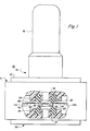
- a piezoresistive pressure transducer 10 includes an enclosure or housing comprising a body 11 having a side wall 12 and open at the top 13 and the bottom.
- Body 11 also includes a plurality of electrical conductors extending through wall 12, the conductors having outer ends 14a and inner ends 14b. The conductors pass through wall 12 along an indirect route as will be described in greater detail later.
- a cover 16 closes first opening 13, and comprises a plate 17 which at least partially fits into opening 13 and a tubing connector 18 formed to snugly fit into the end of a section of tubing carrying pressure to be measured.
- a hole 19 passes through cover 16 into the interior of body 11.
- the bottom opening in body 11 is closed with a cover 20, identical to cover 16 except that cover 20 is not provided with a tubing connector such as connector 18, but is instead provided with a hole 21 for providing an atmospheric pressure reference against which the gauge pressure in the tubing connected to connector 18 can be measured.
- the top and bottom openings in body 11 are identical and covers 16 and 20 may be interchanged, or two identical covers of either type may be used depending on the intended application of the transducer.
- Body 11 and covers 16 and 20 are formed of a thermoplastic material and may be ultrasonically welded together.
- Opening 13 has an intermediate shoulder 22 which forms the transition between the outer part of opening 13 and a slightly smaller inner part of the opening. Such a configuration facilitates the insertion of cover 16 and provides a close tolerance fit when the cover is inserted, to produce a secure weld when the parts are ultrasonically joined.
- cover 20 is formed with a circular channel or groove 25 around hole 21, and cover 16 has a similar channel.
- the channels comprise seats for circular elastomeric seals 26 and 27, which are premoulded to a desired configuration which will be described in greater detail, and cured in that configuration.
- covers 16 and 20 are configured with lips 28 and 29 surrounding channels 24 and 25 respectively.
- the lips are initially formed so that the outer walls of the channels are straight. However, after insertion of seals 26 and 27, the lips are swaged against the bevelled surfaces of the seals to insure that the seals remain securely seated.
- a square chip 32 of semiconductor material, such as silicon, has a circular area of reduced thickness therein to form a central diaphragm 33.
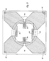
- the upper surface of chip 32 is doped to provide an arrangement of piezoresistors and other conductive regions therein. The dopant pattern will be described in greater detail in connection with Figure 3.
- Chip 32 with the piezoresistors therein forms a stress sensitive element comprising a central diaphragm portion and a thickened rim.
- Chip 32 is gripped at its rim or peripheral portion between seals 26 and 27 whose ends in contact with the chip have reduced outer diameters corresponding to the dimension between the edges of the chip.
- the seals are formed with increased diameters remote from chip 32 to facilitate handling of the seals because the dimensions of the chip and other transducer parts are small (typically a few mm or less).
- the electrically conductive regions in chip 32 are brought to the surface of the chip at the corners thereof outside seal 26. Electrical jumpers 34 are bonded to the chip at the corners thereof, and extend to interior ends of conductors 14b.
- the various parts of transducer 10 are designed so that. the dimensions and spacings of the parts provide for a 10 to 35% compression of seals 26 and 27. This has been found sufficient to provide a satisfactory seal while avoiding the imposition of mechancial stresses on chip 32 which are large enough to adversely affect its output signal.
- the shading represents the doped pattern in the upper surface of chip 32.
- the portions 34 and 35 of the pattern form piezoresistors sensitive to radial and lateral strain respectively.
- These piezoresistors are interconnected by means of conductive regions 36 into a Wheatstone bridge configuration. Regions 36 also provide for electrical communication with external circuitry. Specifically, electrically conductive regions 36 are brought to the surface of chip 32. at locations 37, where they are bonded to jumpers 34 as indicated in connection with Figures 1 and 2. It is pointed out that because of the locations at which the jumpers are bonded to conductive regions 36, these connections are not exposed to fluids or contaminants which might cause adverse effects.
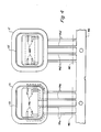
- FIG. 4 illustrates two identical enclosure bodies 11 and 11' connected to a carrier strip 40 of which portions form electrical conductors 14a, 14b and 14a', 14b'.
- the condutors are formed and the bodies are moulded around the conductors so that the conductors follow an indirect route, as shown in the left hand enclosure body, between the exterior and interior thereof. This indirect routing helps to insure a good seal between the body and the conductors.
- the bodies can be reeled onto a reel used in an automatic assembly machine.
- a metal tape 42 of which portions have been etched away provides a lead from 43 comprising electrical jumpers 34 attached to a carrier.
- Jumpers 34 are configured with stress relief sections 44 which minimize the transmission of any stresses to chip 32.
- the output signal of the stress sensitive element is not unduly affected by stresses transmitted through the electrical connections.
- a chip 32 is positioned in registration with jumpers 34 in a lead frame 43 and the free ends of the jumpers are thermocompression bonded to the corner conductive pads on the chip.
- Jumpers 34 are then severed from the remainder of lead frame 34 as indicated at 45.
- a chip with jumpers attached is then positioned within an enclosure body 11 and the outer ends of jumpers 34 are soldered to the inner ends of conductors 14b.
- a pair of elastomeric seals 26 and 27 are then inserted into the channel seats in covers such as 16 and 20, and the lips surrounding the channels swaged to secure the seals in place.
- the covers are then inserted into the openings in the enclosure body and ultrasonically welded in place. Finally, the electrical conductors are severed from carrier strip 40, as indicated at 46 in Figure 4.
- the seals may be formed of any of a wide variety of elastomeric materials. Since some known elastomeric material compatible with almost any fluid can be produced in premoulded form, the present design is adaptable to a wide range of applications. In addition, minor alterations in the selection of parts permits a pressure transducer of the present design to be used in measuring gauge, difference or absolute pressure applications.
- Figure 6 illustrates the modifications necessary for use in absolute pressure sensing applications; the parts common to the embodiment of Figures 1 and 2 are identified by the same reference numerals with the addition of double prime notations.
- the embodiment of Figure 6 differs from the embodiment of Figures 1 and 2 primarily in that glass cover 48 is bonded to the side of chip 32" opposite diaphragm 33" while the space within the rim of the chip is evacuated so as to provide a vacuum reference. The only remaining difference involves minor alterations of parts, dimensions and/or spacings to accommodate the thickness of glass plate 48.
Abstract
Description
- The present invention relates to semiconductor pressure sensing apparatus employing a piezoresistive stress sensitive element.
- It is well known to package piezoresistive stress sensitive elements so that they are adapted to sense fluid pressure. In order to obtain an output indicative of fluid pressure, such a stress sensitive element must be interfaced with other structure in at least two respects which may have significant effects on the output of the element. Specifically, the element must be mechanically supported, and a fluid tight joint must be provided between the element and the support structure to enable fluid pressures to produce a force difference between different portions (typically opposite sides) of the element.
- The quality requirements for the fluid tight joint may vary depending on the intended application of the pressure sensing assembly. A hermetic seal is generally required for high pressures or sensing pressures from low capacity static sources. Hermetic sealing can normally be achieved only with a hard seal, such as produced by soldering, welding thermocompression bonding, electrostatic bonding, etc. For lower pressure applications involving constantly changing pressures or high capacity static sources, forming the joint with an adhesive or soft seal may be suitable.
- In any event, care must be taken to minimize stresses applied to the stress sensitive element by the seal and/or any mounting structure. Stresses in the stress sensitive element may be created by differences in the thermal coefficients of expansion of the element and any structure bonded thereto. Such stresses may also result from aging and contraction of adhesives and/or the force required to grip the stress sensitive element between seals.
- A further disadvantage associated with adhesives is that they must be applied in an uncured form in which they are relatively fluid. Consequently, it is difficult to assure close control over the cured adhesive configuration, as is necessary to achieve satisfactory and consistent performance from piezoresistive transducers. The small size of the semiconductor chips and other transducer parts (typically a few mm or less) increases the difficulty in achieving adequate control over the adhesive. Further, depending on the geometry of the parts, the uncured adhesive may tend to flow into depressions and cavities in which it is unwanted. Finally, the most common adhesives which exhibit satisfactory elasticity and other required characteristics when cured are not compatible with some fluids whose pressures must be sensed.
- It should be noted that because the basic differences in the mechanisms by which pressure is sensed in piezoresistive stress sensitive elements and in other sensors, such as capacitive pressure cells, mounting and pressure seal techniques suitable for capacitive and other types of transducers may be difficult to implement satisfactorily in piezoresistive transducers. A reason for this is that in a capacitive transducer, the region of maximum sensitivity is at the center of a diaphragm structure. Therefore, a capacitive pressure cell may be readily gripped or supported and/or a pressure seal provided at the periphery of the cell without producing an unacceptable effect on the transducer output signal. Conversely, a piezoresistive stress sensitive element is quite sensitive to forces applied at the periphery of its diaphragm. Therefore, the materials used for mounting means and pressure seals must be carefully chosen and the mounting means and seals carefully designed to avoid unaccaptable effects on the output signal.
- An apparent solution is to design the piezoresistive stress sensitive element such that the active diaphragm area with the piezoresesitve device thereon is relatively small in diameter, and that the mounting and pressure seal is located at a substantially larger distance from the centre of the diaphragm. Such an approach has several problems, including a requirement for a larger semiconductor chip which is expensive, increased physical size of the completed transducer when miniaturization may be preferred or required, and/or reduced sensitivity due to the small active diaphragm area.
- A further consideration in the design of a piezoresistive pressure transducer involves insuring that the transducer is compatible with fluids whose pressures are to be sensed, and providing that the sensor design is compatible with as wide a range of fluids as possible. With reference to the semiconductor chip, the most critical area is that at which external electrical connections are made with the doped circuit elements. It is known to use a variety of conformal coatings to protect the electrical connections, as well as other chip features. For silicon substrates such coatings include varnishes, dimethyl silicon, silicon dioxide and silicon nitride.
- Coatings such as varnishes are subject to aging effects and can affect transducer sensitivity and repeatability. Dimethyl silicon can also affect transducer sensitivity, repeatability, and response. With regard to silicon dioxide and silicon nitride, in order to facilitate the application, the coating is normally formed over the entire silicon surface rather than just the interface between the doped circuit elements and external conductors. As noted in U.S. patent 3,417,361 issued to H. Heller et al on 17th December, 1968, and discussed in detail in U.S. patent 4,125,820 to J. Marshall on 14th November, 1978, most metals are at least somewhat soluble in silicon, and silicon dioxide or silicon nitride will, during its formation, take up some kinds of dopants from the semiconductor substrate. This may alter the dopant concentration in the piezoresistors and/or other doped elements, and affect transducer performance. In addition, most usual coating materials (including silicon dioxide and silicon nitride) have significantly different thermal coefficients of expansion from silicon. The use of such coatings may result in thermal stresses which, in turn, will be reflected in the transducer output signal.
- A further important consideration in pressure transducer design is an increasing demand for general cost reductions and for low cost transducers which meet moderate performance requirements. Thus, it has become increasingly important to devise piezoresistive pressure transducer designs which are adaptable for various modes of operation and usable with a variety of fluid media. Finally, low cost generally implies a design which utilizes low cost materials and is adaptable to automated assembly.
- Accordingly, the present invention provides a pressure transducer assembly comprising a diaphragm of semiconductor material having piezoresistive means formed thereon, and a housing in which the diaphragm is mounted so as to form a fluid tight divider between two pressure chambers and having a pressure port to at least one of the chambers,
- characterized in that
- the housing has two inner end surfaces each configured to form a seal seat;
- there are two elastomeric sealing rings each mounted between a respective seal seat and the central region of the diaphragm to form the two pressure chambers;
- and the diaphragm has its piezoresistive means disposed in its cental region and electrically coupled to its periphery, with connecting leads being connected through the housing to its periphery.
- Two embodiments of the invention and a method of manufacture will now be described, by way of example, with reference to the drawings in which:
- Figure 1 is a side view of one embodiment of a piezoresistive pressure transducer, a portion of the housing being broken away to show internal details;
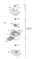
- Figure 2 is an exploded view of the transducer of Figure 1;
- Figure 3 is a plan view of a semiconductor stress sensitive element used in the transducer of Figures 1 and 2;
- Figure 4 is a plan view of two indentical enclosure bodies with electrical conductors connected to a continuous carrier strip used in assembling the transducer of Figure 1 and 2 by automatic assembly processes;
- Figure 5 is a plan view of a section of continuous metal tape which forms connected lead frames used in automatic assembly of the transducer of Figures 1 and 2; and
- Figure 6 is a partial sectional view of a piezoresistive pressure transducer configured for sensing absolute pressure.
- The present transducer is a low cost piezoresistive pressure transducer utilizing premoulded elastomeric seals. The design reduces the need for protective coatings by locating the piezoresistive element-external circuitry interface outside of the area contacted by the fluid whose presure is being sensed, and is well suited for automated assembly.
- The transducer assembly basically comprises a semiconductor diaphragm having a piezoresistive device on a central portion thereof and conductive regions extending from the piezoresistive device to a peripheral portion of the diaphragm, the diaphragm being contained in a housing having a pressure port therein and a pair of opposing internal surfaces on opposite sides of the diaphragm configured to form seats for seals. A premoulded elastomeric seal is located between each seat and the adjacent side of the diaphragm, and electrical conductors extend from the conductive regions at the peripheral portion of the diaphragm to the exterior of the housing.
- The housing may comprise a side wall having a pair of opposing openings which are sealed with covers formed with the seats and one or more pressure ports. The diaphragm may be configured with a thickened rim so as to form a depression which may be evacuated and sealed with a glass plate to provide an absolute pressure reference. The electrical conductors may be arranged to pass through the side wall of the housing along an indirect route to reduce the possibility of leakage.
- The method of manufacture basically comprises fabricating a semiconductor diaphragm having a piezoresistive stress sensitive device formed on its central portion and a peripheral portion to which electrically conductive regions are extended, and forming an enclosure having at least one opening and a cover for closing the opening. The enclosure is configured to house the diaphragm and has a pair of internal surfaces on opposite sides thereof, the internal surfaces each being formed with a seat for a seal. The stress sensitive element is positioned within the housing and electrical jumpers are connected between the conductive regions on the element and conductors in the enclosure. A premoulded elastomeric seal is then positioned between each of the internal surfaces and the adjacent side of the diaphragm, and finally the opening in the enclosure is closed with the cover.
- The jumpers may be formed as part of a lead frame in a connected succession of such lead frames. Similarly, the enclosure, exclusive of the covers, may be one of a succession of such items on a carrier strip used in an automated assembly process in which a semiconductor diaphragm is bonded to each lead frame, the jumpers severed from the remainder of the lead frame, the diaphragm with jumpers attached positioned within the enclosure, the jumpers bonded to electrical conductors in the enclosure, the seals fitted to the covers, the covers bonded to the remainder of the enclosure, and the completed transducer severed from the carrier strip.
- Referring to Figures 1 and 2, a
piezoresistive pressure transducer 10 includes an enclosure or housing comprising a body 11 having aside wall 12 and open at thetop 13 and the bottom. Body 11 also includes a plurality of electrical conductors extending throughwall 12, the conductors havingouter ends 14a andinner ends 14b. The conductors pass throughwall 12 along an indirect route as will be described in greater detail later. - A
cover 16 closes first opening 13, and comprises aplate 17 which at least partially fits intoopening 13 and atubing connector 18 formed to snugly fit into the end of a section of tubing carrying pressure to be measured. Ahole 19 passes throughcover 16 into the interior of body 11. - The bottom opening in body 11 is closed with a
cover 20, identical to cover 16 except thatcover 20 is not provided with a tubing connector such asconnector 18, but is instead provided with ahole 21 for providing an atmospheric pressure reference against which the gauge pressure in the tubing connected toconnector 18 can be measured. - As shown, the top and bottom openings in body 11 are identical and covers 16 and 20 may be interchanged, or two identical covers of either type may be used depending on the intended application of the transducer. Body 11 and covers 16 and 20 are formed of a thermoplastic material and may be ultrasonically welded together.
Opening 13 has anintermediate shoulder 22 which forms the transition between the outer part ofopening 13 and a slightly smaller inner part of the opening. Such a configuration facilitates the insertion ofcover 16 and provides a close tolerance fit when the cover is inserted, to produce a secure weld when the parts are ultrasonically joined. - The inner surface of
cover 20 is formed with a circular channel or groove 25 aroundhole 21, and cover 16 has a similar channel. The channels comprise seats for circularelastomeric seals - The interior surfaces of
covers lips channels seals - A
square chip 32 of semiconductor material, such as silicon, has a circular area of reduced thickness therein to form acentral diaphragm 33. The upper surface ofchip 32 is doped to provide an arrangement of piezoresistors and other conductive regions therein. The dopant pattern will be described in greater detail in connection with Figure 3. -
Chip 32 with the piezoresistors therein forms a stress sensitive element comprising a central diaphragm portion and a thickened rim.Chip 32 is gripped at its rim or peripheral portion betweenseals chip 32 to facilitate handling of the seals because the dimensions of the chip and other transducer parts are small (typically a few mm or less). - The electrically conductive regions in
chip 32 are brought to the surface of the chip at the corners thereof outsideseal 26.Electrical jumpers 34 are bonded to the chip at the corners thereof, and extend to interior ends ofconductors 14b. The various parts oftransducer 10 are designed so that. the dimensions and spacings of the parts provide for a 10 to 35% compression ofseals chip 32 which are large enough to adversely affect its output signal. - With reference to Figure 3, the shading represents the doped pattern in the upper surface of
chip 32. Theportions conductive regions 36 into a Wheatstone bridge configuration.Regions 36 also provide for electrical communication with external circuitry. Specifically, electricallyconductive regions 36 are brought to the surface ofchip 32. atlocations 37, where they are bonded tojumpers 34 as indicated in connection with Figures 1 and 2. It is pointed out that because of the locations at which the jumpers are bonded toconductive regions 36, these connections are not exposed to fluids or contaminants which might cause adverse effects. - A piezoresistive pressure transducer of the present design is well adapted for production from inexpensive materials by means of automatic assembly processes. Figure 4 illustrates two identical enclosure bodies 11 and 11' connected to a
carrier strip 40 of which portions formelectrical conductors - In Figure 5, a
metal tape 42 of which portions have been etched away provides a lead from 43 comprisingelectrical jumpers 34 attached to a carrier.Jumpers 34 are configured withstress relief sections 44 which minimize the transmission of any stresses to chip 32. Thus, the output signal of the stress sensitive element is not unduly affected by stresses transmitted through the electrical connections. - In the automatic assembly process, a
chip 32 is positioned in registration withjumpers 34 in alead frame 43 and the free ends of the jumpers are thermocompression bonded to the corner conductive pads on the chip.Jumpers 34 are then severed from the remainder oflead frame 34 as indicated at 45. A chip with jumpers attached is then positioned within an enclosure body 11 and the outer ends ofjumpers 34 are soldered to the inner ends ofconductors 14b. - A pair of
elastomeric seals carrier strip 40, as indicated at 46 in Figure 4. - It will be apparent that all electrical connections are made at a location not exposed to a fluid whose pressure is being measured. Further, the electrical connections are made in an area sealed from the environment surrounding the pressure transducer. Thus, the need for and problems associated with protective coatings are reduced. In addition, the seals may be formed of any of a wide variety of elastomeric materials. Since some known elastomeric material compatible with almost any fluid can be produced in premoulded form, the present design is adaptable to a wide range of applications. In addition, minor alterations in the selection of parts permits a pressure transducer of the present design to be used in measuring gauge, difference or absolute pressure applications.
- Figure 6 illustrates the modifications necessary for use in absolute pressure sensing applications; the parts common to the embodiment of Figures 1 and 2 are identified by the same reference numerals with the addition of double prime notations. The embodiment of Figure 6 differs from the embodiment of Figures 1 and 2 primarily in that
glass cover 48 is bonded to the side ofchip 32" oppositediaphragm 33" while the space within the rim of the chip is evacuated so as to provide a vacuum reference. The only remaining difference involves minor alterations of parts, dimensions and/or spacings to accommodate the thickness ofglass plate 48.
Claims (9)
Applications Claiming Priority (2)
| Application Number | Priority Date | Filing Date | Title |
|---|---|---|---|
| US06/726,743 US4656454A (en) | 1985-04-24 | 1985-04-24 | Piezoresistive pressure transducer with elastomeric seals |
| US726743 | 2000-11-30 |
Publications (3)
| Publication Number | Publication Date |
|---|---|
| EP0202786A2 true EP0202786A2 (en) | 1986-11-26 |
| EP0202786A3 EP0202786A3 (en) | 1987-09-30 |
| EP0202786B1 EP0202786B1 (en) | 1990-06-27 |
Family
ID=24919826
Family Applications (1)
| Application Number | Title | Priority Date | Filing Date |
|---|---|---|---|
| EP86303078A Expired - Lifetime EP0202786B1 (en) | 1985-04-24 | 1986-04-23 | Piezoresistive pressure transducer |
Country Status (4)
| Country | Link |
|---|---|
| US (1) | US4656454A (en) |
| EP (1) | EP0202786B1 (en) |
| JP (1) | JPS61247933A (en) |
| DE (1) | DE3672301D1 (en) |
Cited By (9)
| Publication number | Priority date | Publication date | Assignee | Title |
|---|---|---|---|---|
| FR2619446A1 (en) * | 1987-08-14 | 1989-02-17 | Gulton Ind Inc | STRAIN GAUGE |
| EP0317664A1 (en) * | 1987-11-27 | 1989-05-31 | Kristal Instrumente AG | Measurement cell, particularly for measurements of relative and differential pressure |
| EP0519817A1 (en) * | 1991-06-18 | 1992-12-23 | Jaeger | Supporting device for the capsule of an electrical transducer |
| EP0552017A2 (en) * | 1992-01-13 | 1993-07-21 | Mitsubishi Denki Kabushiki Kaisha | Semiconductor pressure sensor and method of manufacturing same |
| WO1998000692A1 (en) * | 1996-06-28 | 1998-01-08 | Siemens Aktiengesellschaft | Pressure sensor for mounting on the components side of a printed circuit board |
| WO1998000691A1 (en) * | 1996-06-28 | 1998-01-08 | Siemens Aktiengesellschaft | Semiconductor device |
| WO2015038320A1 (en) * | 2013-09-12 | 2015-03-19 | Honeywell International Inc. | Media isolated pressure sensor |
| EP2120029A3 (en) * | 2008-05-14 | 2016-06-29 | Honeywell International Inc. | Asic compensated pressure sensor with soldered sense die attach |
| WO2019190796A1 (en) * | 2018-03-29 | 2019-10-03 | Veoneer Us Inc. | Rectangular snap fit pressure sensor unit |
Families Citing this family (53)
| Publication number | Priority date | Publication date | Assignee | Title |
|---|---|---|---|---|
| EP0215140B1 (en) * | 1985-09-11 | 1989-04-26 | Kunz, Manfred | Pressure sensor |
| US4772217A (en) * | 1987-06-30 | 1988-09-20 | Augat Inc. | Pressure sensor connector system |
| US4756193A (en) * | 1987-09-11 | 1988-07-12 | Delco Electronics Corporation | Pressure sensor |
| US4879903A (en) * | 1988-09-02 | 1989-11-14 | Nova Sensor | Three part low cost sensor housing |
| US5048181A (en) * | 1988-09-19 | 1991-09-17 | Ford Motor Company | Method for making thick film circuit housing assembly design |
| US4923444A (en) * | 1988-12-19 | 1990-05-08 | Ivac Corporation | Negative pressure measurement system |
| US4942383A (en) * | 1989-03-06 | 1990-07-17 | Honeywell Inc. | Low cost wet-to-wet pressure sensor package |
| DE3937522A1 (en) * | 1989-11-10 | 1991-05-16 | Texas Instruments Deutschland | SEMICONDUCTOR PRESSURE SENSOR CONNECTED TO A CARRIER ELEMENT |
| US5121627A (en) * | 1990-05-21 | 1992-06-16 | Aoust Brian G D | Integrated miniaturized sensor for measuring total dissolved gas and liquid vapor |
| CA2058916C (en) * | 1991-01-28 | 2000-03-21 | Dean Joseph Maurer | Piezoresistive pressure transducer with a conductive elastomeric seal |
| US5184107A (en) * | 1991-01-28 | 1993-02-02 | Honeywell, Inc. | Piezoresistive pressure transducer with a conductive elastomeric seal |
| US5187985A (en) * | 1991-09-19 | 1993-02-23 | Honeywell Inc. | Amplified pressure transducer |
| US5351550A (en) * | 1992-10-16 | 1994-10-04 | Honeywell Inc. | Pressure sensor adapted for use with a component carrier |
| US5327785A (en) * | 1993-03-09 | 1994-07-12 | Honeywell Inc. | Pressure sensor with improved heat dissipation characteristics |
| US5410916A (en) * | 1994-06-24 | 1995-05-02 | Honeywell Inc. | Flowthrough pressure sensor |
| US5644285A (en) * | 1995-02-01 | 1997-07-01 | Honeywell Inc. | Pressure transducer with media isolation |
| US5483994A (en) * | 1995-02-01 | 1996-01-16 | Honeywell, Inc. | Pressure transducer with media isolation and negative pressure measuring capability |
| US5763787A (en) * | 1996-09-05 | 1998-06-09 | Rosemont Inc. | Carrier assembly for fluid sensor |
| DE19707503B4 (en) * | 1997-02-25 | 2007-01-04 | Infineon Technologies Ag | Pressure sensor component and method of manufacture |
| US6076409A (en) * | 1997-12-22 | 2000-06-20 | Rosemount Aerospace, Inc. | Media compatible packages for pressure sensing devices |
| US6311561B1 (en) | 1997-12-22 | 2001-11-06 | Rosemount Aerospace Inc. | Media compatible pressure sensor |
| US20020003274A1 (en) * | 1998-08-27 | 2002-01-10 | Janusz Bryzek | Piezoresistive sensor with epi-pocket isolation |
| US6006607A (en) * | 1998-08-31 | 1999-12-28 | Maxim Integrated Products, Inc. | Piezoresistive pressure sensor with sculpted diaphragm |
| US6351996B1 (en) | 1998-11-12 | 2002-03-05 | Maxim Integrated Products, Inc. | Hermetic packaging for semiconductor pressure sensors |
| US6346742B1 (en) | 1998-11-12 | 2002-02-12 | Maxim Integrated Products, Inc. | Chip-scale packaged pressure sensor |
| US6229190B1 (en) | 1998-12-18 | 2001-05-08 | Maxim Integrated Products, Inc. | Compensated semiconductor pressure sensor |
| US6255728B1 (en) | 1999-01-15 | 2001-07-03 | Maxim Integrated Products, Inc. | Rigid encapsulation package for semiconductor devices |
| DE19909069C2 (en) * | 1999-03-02 | 2001-08-30 | Hahn Schickard Ges | Micro valve arrangement |
| CA2310149C (en) | 2000-05-30 | 2004-12-07 | International Road Dynamics Inc. | In road vehicle axle sensor |
| US6612175B1 (en) | 2000-07-20 | 2003-09-02 | Nt International, Inc. | Sensor usable in ultra pure and highly corrosive environments |
| US7152478B2 (en) * | 2000-07-20 | 2006-12-26 | Entegris, Inc. | Sensor usable in ultra pure and highly corrosive environments |
| US6883874B2 (en) | 2000-09-14 | 2005-04-26 | New York Air Brake Corporation | Pressure sensor module |
| US6889568B2 (en) * | 2002-01-24 | 2005-05-10 | Sensarray Corporation | Process condition sensing wafer and data analysis system |
| US7757574B2 (en) * | 2002-01-24 | 2010-07-20 | Kla-Tencor Corporation | Process condition sensing wafer and data analysis system |
| JP3479064B1 (en) * | 2002-04-12 | 2003-12-15 | 北陸電気工業株式会社 | Semiconductor force sensor |
| JP2004004069A (en) * | 2002-04-12 | 2004-01-08 | Hokuriku Electric Ind Co Ltd | Semiconductor force sensor |
| AU2003295811A1 (en) * | 2002-11-22 | 2004-06-18 | Knowles Electronics, Llc | An apparatus for energy transfer in a balanced receiver assembly and manufacturing method thereof |
| DE10343498A1 (en) * | 2003-02-07 | 2005-05-04 | Univ Leipzig | Method for determining at least one state parameter of a sealing system and sealing system |
| US20040209699A1 (en) * | 2003-04-18 | 2004-10-21 | Olson Roger Allred | Electronic putting target apparatus |
| US7204010B2 (en) * | 2004-04-28 | 2007-04-17 | Measurement Specialties, Inc. | Method of making a load sensor plate |
| US8604361B2 (en) * | 2005-12-13 | 2013-12-10 | Kla-Tencor Corporation | Component package for maintaining safe operating temperature of components |
| JP4939110B2 (en) * | 2006-05-16 | 2012-05-23 | 株式会社ミツトヨ | Probe and surface texture measuring device |
| US8164007B2 (en) * | 2008-07-16 | 2012-04-24 | Honeywell International | Conductive elastomeric seal and method of fabricating the same |
| US7900521B2 (en) * | 2009-02-10 | 2011-03-08 | Freescale Semiconductor, Inc. | Exposed pad backside pressure sensor package |
| US8371176B2 (en) | 2011-01-06 | 2013-02-12 | Honeywell International Inc. | Media isolated pressure sensor |
| US8681493B2 (en) | 2011-05-10 | 2014-03-25 | Kla-Tencor Corporation | Heat shield module for substrate-like metrology device |
| US8516897B1 (en) | 2012-02-21 | 2013-08-27 | Honeywell International Inc. | Pressure sensor |
| US9003897B2 (en) * | 2012-05-10 | 2015-04-14 | Honeywell International Inc. | Temperature compensated force sensor |
| EP2972173A1 (en) | 2013-03-14 | 2016-01-20 | TRL Enterprises LLC | Fully swept pressure sensor |
| WO2015199228A1 (en) * | 2014-06-27 | 2015-12-30 | 北陸電気工業株式会社 | Force detector |
| KR102637239B1 (en) * | 2017-02-27 | 2024-02-19 | 현대모비스 주식회사 | Pressure sensing apparatus for vehicle |
| KR102413739B1 (en) * | 2017-09-15 | 2022-06-29 | 현대모비스 주식회사 | Pressure sensing apparatus for air bag |
| US11292101B2 (en) * | 2017-11-22 | 2022-04-05 | Taiwan Semiconductor Manufacturing Co., Ltd. | Chemical mechanical polishing apparatus and method |
Citations (1)
| Publication number | Priority date | Publication date | Assignee | Title |
|---|---|---|---|---|
| DE3200448A1 (en) * | 1982-01-09 | 1983-07-21 | Philips Patentverwaltung Gmbh, 2000 Hamburg | Semiconductor pressure transducer device |
Family Cites Families (15)
| Publication number | Priority date | Publication date | Assignee | Title |
|---|---|---|---|---|
| US2751530A (en) * | 1954-01-04 | 1956-06-19 | Honeywell Regulator Co | Differential pressure sensing unit |
| US2830698A (en) * | 1955-04-25 | 1958-04-15 | Erie Resistor Corp | Condenser |
| US3315201A (en) * | 1965-03-31 | 1967-04-18 | Bailey Meter Co | Strain transducer |
| US3455165A (en) * | 1965-12-22 | 1969-07-15 | Pierre Huet | Pressure sensitive devices |
| US3417361A (en) * | 1966-03-07 | 1968-12-17 | Conrac Corp | Semiconductive pressure transducer |
| US3466513A (en) * | 1968-01-24 | 1969-09-09 | William R Belko Jr | Electrical capacitor |
| US3739315A (en) * | 1972-05-18 | 1973-06-12 | Kulite Semiconductors Prod Inc | Semiconductor transducers having h shaped cross-sectional configurations |
| NL7415668A (en) * | 1974-12-02 | 1976-06-04 | Philips Nv | PRESSURE TRANSMITTER. |
| US4125820A (en) * | 1975-10-06 | 1978-11-14 | Honeywell Inc. | Stress sensor apparatus |
| US4128006A (en) * | 1976-12-13 | 1978-12-05 | Bunker Ramo Corporation | Packaging of pressure sensor cells |
| US4173900A (en) * | 1977-03-07 | 1979-11-13 | Hitachi, Ltd. | Semiconductor pressure transducer |
| JPS54131892A (en) * | 1978-04-05 | 1979-10-13 | Hitachi Ltd | Semiconductor pressure converter |
| ATE7737T1 (en) * | 1980-02-06 | 1984-06-15 | Hans W. Dipl.-Phys. Keller | PIEZORESISTIVE CYLINDER CAN LIKE PRESSURE GAUGE. |
| US4528855A (en) * | 1984-07-02 | 1985-07-16 | Itt Corporation | Integral differential and static pressure transducer |
| US4600912A (en) * | 1985-01-25 | 1986-07-15 | Bourns Instruments, Inc. | Diaphragm pressure sensor with improved tensile loading characteristics |
-
1985
- 1985-04-24 US US06/726,743 patent/US4656454A/en not_active Expired - Lifetime
-
1986
- 1986-04-23 DE DE8686303078T patent/DE3672301D1/en not_active Expired - Fee Related
- 1986-04-23 EP EP86303078A patent/EP0202786B1/en not_active Expired - Lifetime
- 1986-04-23 JP JP61094406A patent/JPS61247933A/en active Pending
Patent Citations (1)
| Publication number | Priority date | Publication date | Assignee | Title |
|---|---|---|---|---|
| DE3200448A1 (en) * | 1982-01-09 | 1983-07-21 | Philips Patentverwaltung Gmbh, 2000 Hamburg | Semiconductor pressure transducer device |
Non-Patent Citations (2)
| Title |
|---|
| ELECTRONIC ENGINEERING, vol. 53, no. 659, November 1981, page 169, London, GB; E. BOSE: "Fluid pressure transducers" * |
| MACHINE DESIGN, vol. 55, no. 5, March 1983, page 64, Cleveland, Ohio, US; "Upside-down sensor takes turbocharger-abuse" * |
Cited By (16)
| Publication number | Priority date | Publication date | Assignee | Title |
|---|---|---|---|---|
| FR2619446A1 (en) * | 1987-08-14 | 1989-02-17 | Gulton Ind Inc | STRAIN GAUGE |
| GB2208715A (en) * | 1987-08-14 | 1989-04-12 | Gulton Ind Inc | Improved strain gage |
| GB2208715B (en) * | 1987-08-14 | 1991-10-23 | Gulton Ind Inc | Improved strain gage |
| EP0317664A1 (en) * | 1987-11-27 | 1989-05-31 | Kristal Instrumente AG | Measurement cell, particularly for measurements of relative and differential pressure |
| EP0519817A1 (en) * | 1991-06-18 | 1992-12-23 | Jaeger | Supporting device for the capsule of an electrical transducer |
| FR2678066A1 (en) * | 1991-06-18 | 1992-12-24 | Jaeger | SUPPORT DEVICE FOR AN ELECTRIC SENSOR CAPSULE. |
| EP0552017A2 (en) * | 1992-01-13 | 1993-07-21 | Mitsubishi Denki Kabushiki Kaisha | Semiconductor pressure sensor and method of manufacturing same |
| EP0552017A3 (en) * | 1992-01-13 | 1994-02-09 | Mitsubishi Electric Corp | |
| WO1998000692A1 (en) * | 1996-06-28 | 1998-01-08 | Siemens Aktiengesellschaft | Pressure sensor for mounting on the components side of a printed circuit board |
| WO1998000691A1 (en) * | 1996-06-28 | 1998-01-08 | Siemens Aktiengesellschaft | Semiconductor device |
| US6313729B1 (en) | 1996-06-28 | 2001-11-06 | Siemens Aktiengesellschaft | Semiconductor device |
| EP2120029A3 (en) * | 2008-05-14 | 2016-06-29 | Honeywell International Inc. | Asic compensated pressure sensor with soldered sense die attach |
| WO2015038320A1 (en) * | 2013-09-12 | 2015-03-19 | Honeywell International Inc. | Media isolated pressure sensor |
| US9470593B2 (en) | 2013-09-12 | 2016-10-18 | Honeywell International Inc. | Media isolated pressure sensor |
| WO2019190796A1 (en) * | 2018-03-29 | 2019-10-03 | Veoneer Us Inc. | Rectangular snap fit pressure sensor unit |
| US10942079B2 (en) | 2018-03-29 | 2021-03-09 | Veoneer Us Inc. | Rectangular snap fit pressure sensor unit |
Also Published As
| Publication number | Publication date |
|---|---|
| EP0202786B1 (en) | 1990-06-27 |
| DE3672301D1 (en) | 1990-08-02 |
| US4656454A (en) | 1987-04-07 |
| JPS61247933A (en) | 1986-11-05 |
| EP0202786A3 (en) | 1987-09-30 |
Similar Documents
| Publication | Publication Date | Title |
|---|---|---|
| EP0202786B1 (en) | Piezoresistive pressure transducer | |
| US5184107A (en) | Piezoresistive pressure transducer with a conductive elastomeric seal | |
| US6351996B1 (en) | Hermetic packaging for semiconductor pressure sensors | |
| US5522267A (en) | Modular diaphragm pressure sensor with peripherally mounted electrical terminals | |
| EP0386959B1 (en) | Low cost wet-to-wet pressure sensor package | |
| US4578735A (en) | Pressure sensing cell using brittle diaphragm | |
| US7183620B2 (en) | Moisture resistant differential pressure sensors | |
| US4790192A (en) | Silicon side by side coplanar pressure sensors | |
| US4572000A (en) | Pressure sensor with a substantially flat overpressure stop for the measuring diaphragm | |
| US5483834A (en) | Suspended diaphragm pressure sensor | |
| EP0311612B1 (en) | Capacitance pressure sensor | |
| EP2189773B1 (en) | Design of wet/wet differential pressure sensor based on microelectronic packaging process | |
| US4773269A (en) | Media isolated differential pressure sensors | |
| US6813956B2 (en) | Double stop structure for a pressure transducer | |
| US20030107096A1 (en) | Combined absolute differential transducer | |
| US6612178B1 (en) | Leadless metal media protected pressure sensor | |
| EP0497534B1 (en) | Piezoresistive pressure transducer with a conductive elastomeric seal | |
| US6591686B1 (en) | Oil filled pressure transducer | |
| US5034848A (en) | Low pressure sensor | |
| JPH01248033A (en) | Semiconductor type pressure sensor | |
| JPH07209119A (en) | Pressure sensor | |
| WO2000057151A1 (en) | Capacitive differential pressure sensor | |
| JPH05302863A (en) | Semiconductor pressure sensor | |
| JP2000146736A (en) | Pressure-detecting device | |
| JPH05142077A (en) | Differential pressure measuring device |
Legal Events
| Date | Code | Title | Description |
|---|---|---|---|
| PUAI | Public reference made under article 153(3) epc to a published international application that has entered the european phase |
Free format text: ORIGINAL CODE: 0009012 |
|
| AK | Designated contracting states |
Kind code of ref document: A2 Designated state(s): CH DE LI NL |
|
| PUAL | Search report despatched |
Free format text: ORIGINAL CODE: 0009013 |
|
| AK | Designated contracting states |
Kind code of ref document: A3 Designated state(s): CH DE LI NL |
|
| 17P | Request for examination filed |
Effective date: 19880317 |
|
| 17Q | First examination report despatched |
Effective date: 19881227 |
|
| GRAA | (expected) grant |
Free format text: ORIGINAL CODE: 0009210 |
|
| AK | Designated contracting states |
Kind code of ref document: B1 Designated state(s): CH DE LI NL |
|
| REF | Corresponds to: |
Ref document number: 3672301 Country of ref document: DE Date of ref document: 19900802 |
|
| PLBE | No opposition filed within time limit |
Free format text: ORIGINAL CODE: 0009261 |
|
| STAA | Information on the status of an ep patent application or granted ep patent |
Free format text: STATUS: NO OPPOSITION FILED WITHIN TIME LIMIT |
|
| 26N | No opposition filed | ||
| PGFP | Annual fee paid to national office [announced via postgrant information from national office to epo] |
Ref country code: DE Payment date: 19920321 Year of fee payment: 7 |
|
| PGFP | Annual fee paid to national office [announced via postgrant information from national office to epo] |
Ref country code: CH Payment date: 19920324 Year of fee payment: 7 |
|
| PGFP | Annual fee paid to national office [announced via postgrant information from national office to epo] |
Ref country code: NL Payment date: 19920430 Year of fee payment: 7 |
|
| PG25 | Lapsed in a contracting state [announced via postgrant information from national office to epo] |
Ref country code: LI Effective date: 19930430 Ref country code: CH Effective date: 19930430 |
|
| PG25 | Lapsed in a contracting state [announced via postgrant information from national office to epo] |
Ref country code: NL Effective date: 19931101 |
|
| NLV4 | Nl: lapsed or anulled due to non-payment of the annual fee | ||
| REG | Reference to a national code |
Ref country code: CH Ref legal event code: PL |
|
| PG25 | Lapsed in a contracting state [announced via postgrant information from national office to epo] |
Ref country code: DE Effective date: 19940101 |