EP0193856A2 - IC card - Google Patents
IC card Download PDFInfo
- Publication number
- EP0193856A2 EP0193856A2 EP86102478A EP86102478A EP0193856A2 EP 0193856 A2 EP0193856 A2 EP 0193856A2 EP 86102478 A EP86102478 A EP 86102478A EP 86102478 A EP86102478 A EP 86102478A EP 0193856 A2 EP0193856 A2 EP 0193856A2
- Authority
- EP
- European Patent Office
- Prior art keywords
- sheet
- chip
- card
- connection pads
- card according
- Prior art date
- Legal status (The legal status is an assumption and is not a legal conclusion. Google has not performed a legal analysis and makes no representation as to the accuracy of the status listed.)
- Granted
Links
Images


Classifications
-
- G—PHYSICS
- G06—COMPUTING; CALCULATING OR COUNTING
- G06K—GRAPHICAL DATA READING; PRESENTATION OF DATA; RECORD CARRIERS; HANDLING RECORD CARRIERS
- G06K19/00—Record carriers for use with machines and with at least a part designed to carry digital markings
- G06K19/06—Record carriers for use with machines and with at least a part designed to carry digital markings characterised by the kind of the digital marking, e.g. shape, nature, code
- G06K19/067—Record carriers with conductive marks, printed circuits or semiconductor circuit elements, e.g. credit or identity cards also with resonating or responding marks without active components
- G06K19/07—Record carriers with conductive marks, printed circuits or semiconductor circuit elements, e.g. credit or identity cards also with resonating or responding marks without active components with integrated circuit chips
- G06K19/077—Constructional details, e.g. mounting of circuits in the carrier
- G06K19/07745—Mounting details of integrated circuit chips
-
- G—PHYSICS
- G06—COMPUTING; CALCULATING OR COUNTING
- G06K—GRAPHICAL DATA READING; PRESENTATION OF DATA; RECORD CARRIERS; HANDLING RECORD CARRIERS
- G06K19/00—Record carriers for use with machines and with at least a part designed to carry digital markings
- G06K19/06—Record carriers for use with machines and with at least a part designed to carry digital markings characterised by the kind of the digital marking, e.g. shape, nature, code
- G06K19/067—Record carriers with conductive marks, printed circuits or semiconductor circuit elements, e.g. credit or identity cards also with resonating or responding marks without active components
- G06K19/07—Record carriers with conductive marks, printed circuits or semiconductor circuit elements, e.g. credit or identity cards also with resonating or responding marks without active components with integrated circuit chips
- G06K19/077—Constructional details, e.g. mounting of circuits in the carrier
- G06K19/07743—External electrical contacts
-
- H—ELECTRICITY
- H01—ELECTRIC ELEMENTS
- H01L—SEMICONDUCTOR DEVICES NOT COVERED BY CLASS H10
- H01L2924/00—Indexing scheme for arrangements or methods for connecting or disconnecting semiconductor or solid-state bodies as covered by H01L24/00
- H01L2924/0001—Technical content checked by a classifier
- H01L2924/0002—Not covered by any one of groups H01L24/00, H01L24/00 and H01L2224/00
-
- Y—GENERAL TAGGING OF NEW TECHNOLOGICAL DEVELOPMENTS; GENERAL TAGGING OF CROSS-SECTIONAL TECHNOLOGIES SPANNING OVER SEVERAL SECTIONS OF THE IPC; TECHNICAL SUBJECTS COVERED BY FORMER USPC CROSS-REFERENCE ART COLLECTIONS [XRACs] AND DIGESTS
- Y10—TECHNICAL SUBJECTS COVERED BY FORMER USPC
- Y10S—TECHNICAL SUBJECTS COVERED BY FORMER USPC CROSS-REFERENCE ART COLLECTIONS [XRACs] AND DIGESTS
- Y10S283/00—Printed matter
- Y10S283/904—Credit card
Abstract
Description
- This invention relates to IC cards.
- Recently, various IC cards have been developed, and their improvements have been proposed. United States patent specification 4,216,577 (Bernard et al) discloses such an IC card.. In the disclosed IC card, an IC chip is mounted on a circuit board with terminals, to which signal and power source voltage are supplied. The circuit board with the IC chip is secured to a hard resin sheet, and is covered by a sheet or film having holes, which correspond to and expose the terminals of the circuit board. In this prior art IC card, the terminals which are provided in the holes of the cover sheet are depressed in level from the top surface of the film to an extend substantially corresponding to the thickness of the cover sheet. Therefore, dust is liable to be collected in the holes, giving rise to failure of the electric connection between the IC card terminals and external device.
- The ISO (International Standardization Organization) proposes that four contact segments formed in the IC card are arranged in two rows and the internal between the two rows is 5.62 mm. In the disclosed IC chip noted above, on the other hand, an IC chip is provided between contact rows. With this structure, it is necessary to provided in a 5.62-mm space if the ISO standards are to be conformed. To do so, however, involves difficulties in actual manufacture. In addition, in this structure, probes are contacted to the contacts and the pressure is applied to the contacts from the probes, and this will lead to rupture of the IC chip.
- Further, recently it has been considered to store transaction data in IC chips. Doing so, however, requires an increased memory capacity. This is said to require provision of two IC chips in the IC card.
- An object of the invention is to provide a highly reliable IC card, which can eliminate connection failure due to collection of dust between the IC card terminals and external device.
- According to the invention, there is provided an IC card comprising:
- at least one IC chip having electrical terminals to be connected to an external device;
- a sheet-like structure having one surface and supporting said IC chip;
- internal connecting members formed on said one surface of said sheet-like structure and including a plurality of connection pads and wiring patterns connecting said.connection pads to said electrical terminals of said IC chip;
- a sheet film having openings facing said connection pads and covering said one surface of said sheet-like structure; and
- contact segments formed on said connection pads, having a thickness substantially equal to the thickness of said sheet film and fitted in said first openings.
- This invention can be more fuly understood from the following detailed description when taken in conjunction with the accompanying drawings, in which:
- Fig. 1 is a schematic perspective view showing an embodiment of the IC card according to the invention;
- Fig. 2 is a perspective view showing an IC card shown in Fig. l;
- Fig. 3 is a sectional view taken along line III-III in Fig. 1;
- Fig. 4 is a block diagram showing a circuit struc-_ ture of a main chip and a sub-chip assembled in the structure shown in Fig. 4;
- Fig. 5 is a schematic view showing memory areas of EP-ROM shown in Fig. 4;
- Fig. 6 is a perspective view showing a different embodiment of the IC card according to the invention; and
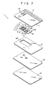
- Fig. 7 is an exploded perspective view showing the IC card shown in Fig. 6.
- Fig. 1 is a perspective view showing an embodiment of IC card 1 according to the invention. This IC card, as shown in Fig. 1, is a rectangular plate having flexibility. It is 85.5 mm in length, 54 mm in width and 0.8 mm in thickness. One of its surfaces, e.g., the front surface, has embossing 2 of the owner's code or name. The other surface, e.g., back surface, has
magnetic stripe 3 having owner's information, e.g., code number or account number. Embossing 2 andmagnetic stripe 3 are provided such that they extend in the longitudinal direction of IC card 1. IC card 1 has a plurality of holes orrecesses 11A, which are formed in an area of the back surface near a longitudinal end portion and substantially in a transversal center. Contacts to be connected to an external device are accommodated inholes 11A. The back surface is substantially flat. IC card 1 accommodatessubstrate 4 withmain chip 5 andsub-chip 6 mounted thereon. - The structure of IC chip 1 shown in Fig. 1 will be described in detail with reference to Figs. 2 and 3. The structure comprises
transparent top sheet 11 of vinyl chloride or polyester. It hasmagnetic stripe 3 formed on the front surface and a decorative impression provided on the rear surface. It has eightholes 11A arranged in two rows each of four holes, the rows being spaced apart by a distance of t = 5.62 mm.Holes 11A have a size conforming to or slightly greater than the ISO standards and are formed at position conforming to the ISO standards. - Disposed under
top sheet 11 issubstrate 4 made of bismaleimide-triazine, glass epoxy resin, etc.Substrate 4 hasholes Main chip 5 andsub-chip 6 having respective internal LSIs (large scale integrated circuits) are accommodated inholes Substrate 4 hasconductor 7.Conductor 7 has connection terminals orpads 7A to be connected to an external circuit and a wiringpattern connecting terminals 7A to terminals ofmain chip 5 andsub-chip 6.Conductor 7 is made of a copper foil. Eachterminal 7A has a greater size than opening llA provided intop sheet 11. Contact segments 7-1 to 7-8 are formed by copper plating onterminals 7A such that they project from the surface ofsubstrate 4. More specifically,conductive foil 7 is formed by copper plating on the substrate, then a plating resist is provided except for portions provided with the contact sections, and then copper plating is provided once again, so that contact segments 7-1 to 7-8 project.Terminals 7A and contact segments 7-1 to 7-8 are preferably covered by gold plating. Contact segments 7-1 to 7-8 have a size substantially equal to or slightly smaller thanhole 11A oftop film 11. More specifically, contact segments 7-1 to 7-8 have a size substantially conforming to ISO standards of a length of 2 mm and a width of 1.7 mm. - Contact segments 7-1 to 7-8 are arranged at interval similar to the case of
holes 11A in two rows each of four lines. When contact segments 7-1 to 7-8 are fitted in holes llA oftop sheet 11,holes 11A are filled with contact segments 7-1 to 7-8. Besides, the areas oftop film 11 whereholes 11A are flush with the rest of the surface, that is, there is no step.. Therefore, no dust particles are collected inholes 11A. In the above described embodiment, each connectingterminals 7A is formed in a larger size than that of each contact segments 7-1, 7-8 so that even it small gaps are produced between the opening 11A and the contact segments, parts of theconnecting terminals 7A are exposed through the gaps. Thereby, IC card always has a good appearance. Contact segments 7-1 to 7-8 constitute VDD terminal 7-1 for power supply, reset terminal 7-2, clock terminal 7-3, GND terminal 7-5, VCC terminal 7-6, to which a voltage is applied when writing transaction information to be described later, and address data input terminal 7-7. Contact segments 7-4 and 7-8 are provided as spare contact sections, and no signal is fed to them in this embodiment. - The connection between terminal of
main chip 5 and wiring pattern 7b is effected when providingpellet 5A on the substrate during manufacture ofmain chip 5.Main chip 5 is fablicated by forming an integrated circuit in a wafer, then providinggold bumpers 5B on the wafer, then dicing the system to separatepellet 5A, then providinglead 5C made of a tin-plated copper foil such that it faces eachgold bumper 5B, and finally effecting inner lead bonding. During this process, lead 5C which is bonded to a tape carrier (not shown) is cut to be separated from the tape carrier. At the time of the separation, one end portion is connected by inner lead bonding togold bumper 5B, and the other end is overlapped overwiring pattern 7B surrounding hole 4A and connected by outer lead bonding thereto. After completion of the connection, a resin is molded on the surface ofmain chip 5, thus completing the main chip. The fablication ofsub-chip 6 and mounting thereof onsubstrate 4 are the same as for the main chip, so their description is omitted.Pellet 6A,gold bumper 6B, lead 6C andresin molding 6D ofsub-chip 6 shown in Fig. 3 correspond topellet 5A,gold bumper 5B, lead 5C andresin molding 5D ofmain chip 5, respectively. - As shown in Fig. 3,
terminals 7A which are connected to contact segments 7-1 to 7-8 extend into throughhole 8.Terminals 7A which are connected to contact segments 7-1 to 7-4, although not clearly shown in Fig. 3, are connected leads ofmain chip 5 throughwiring pattern 7B provided on the back surface ofsubstrate 4.Terminals 7A connected to contact segments 7-5 to 7-8 are connected to leads ofmain chip 5 throughwiring pattern 7B provided on the top surface ofsubstrate 4. -
Substrate 4 withmain chip 5 andsub-chip 6 mounted thereon, is accommodated in anopening 12A ofupper sheet 12, opening 12A having substantially the same size thesubstrate 4.Upper sheet 12 is made of a hard vinyl chloride resin or a polyester resin. It has substantially the same thickness assubstrate 4.Substrate 4 thus is accommodated in opening 12A ofupper sheet 12 substantially in close contact therewith, that is, it has a substantially fixed position relative toupper sheet 12.Main chip 5 andsub-chip 6,. however, have a greater thickness thansubstrate 4. They are thus retained in the substrate with their lower portion projecting therefrom. Therefore, lower portions ofpellets upper sheet 12 with the substrate mounted therein, as shown in Fig. 3.Lower sheet 13 is laminated in close contact with the lower surface ofupper sheet 12.Lower sheet 13 hasholes holes 12A ofupper sheet 12 and substantially the same aspellets holes 12A. When upper andlower sheets pellets upper sheet 12 are snugly received inholes -
Transparent back sheet 14 is provided in close contact with the back surface oflower resin sheet 13. The inner surface ofback sheet 14 has a print of owner's code and owner'sname 14A. Although not shown, the entire surface ofbottom sheet 14 is provided with a decorative print in colors different from the print of owner's code and owner's name. - IC card 1 having the above construction is assembled as follows.
- As has been described above,
conductor 7 consisting of terminal sections orcontact pads 7A andwiring pattern sections 7B are formed onsubstrate 4. Contact segments 7-1 to 7-8 are formed on terminal section 7a such that they projected therefrom.Main chip 5 andsub-chip 6 are then mounted onsubstrate 4 in the manner as described before. Then,bottom sheet 14,lower resin sheet 13 andupper resin sheet 12 are laminated in the mentioned order, andsubstrate 4 withmain chip 5 andsub-chip 6 is set in opening 12A ofupper resin sheet 12. In this state, holes 13A and 13B oflower resin sheet 13correspond pellets upper resin sheet 13 are received inholes Top sheet 11 then is laminated from above. The system thus obtained is then treated with a thermal press. Wheretop sheet 11, upper andlower resin sheets bottom sheet 14 are made of a vinyl chloride resin, the individual sheets are bonded together with the melting of the vinyl chloride resin in the thermal press. Where the sheets are made of polyester, they may be bonded together with an adhesive provided between adjacent ones of them using a press. - Afterwards,
top sheet 11 is embossed to form embossing 14A of the owner's code and owner's name. The electric circuit ofmain chip 5 andsub-chip 6 will now be described with reference to Fig. 4. - In the above embodiment of IC card 1, a data memory part is provided as a separate chip in order to provided an increased data storage capacity of the IC card.
- More specifically,
main chip 5 includesCPU 51,memory 52,decryption circuit 53 andcomparator 54.Subchip 6 has EP-ROM (erasable and programmable read-only memory) 61. Of contact segments 7-1 to 7-8 ofsubstrate 4, those constituting I/O (input/output) terminal, RST (reset) terminal, CLK (clock) terminal and GND terminal are connected tomain chip 5, that constituting Vcc terminal is connected tosub-chip 6, and that constituting VDD terminal is connected tomain chip 5 andsub-chip 6. - EP-
ROM 61 has memory areas as shown in Fig. 5. More specifically, EP-ROM 61 hasidentification data area 70, in which owner's identification data is stored, andapplication data area 80, in which data of the history of transactions using the IC card is stored.Identification data area 70 includes manufacturer's data section, in which data is written by the manufacturer of the IC card, issuer'sdata section 72,' in which data is written by issuer, and owner'sdata section 73, in which data is written by the owner of the IC card. Manufacturer'sdata section 71 has CA (card authenticator)memory area 71 and MPRK (manufacturer's private key code)memory area 71B. InCA memory area 71A is stored an CA code consisting of 64 bits, for instance, which is peculier to each IC card. The CA code is transmitted to a card terminal (not shown) to be used for the computation of SAN (sales approval number). - Issuer's
data section 72 has IPRK (issuer's private key code)memory area 72A, CHN (card holder is name) memory area 72B and ED (expiration date)memory area 72C. Owner'ssection 73 has PIN (private identification number)memory area 73A. Inapplication data area 80, transaction data when a transaction is done using the IC card, e.g., data of the amount of the transaction, date of the transaction, SAN, etc., are stored whenever a transaction is done. The SAN is computed on the terminal side using date data, transaction amount data, etc. as well as the CA code noted above after a predetermined argorithm. The result of the computation is transmitted to and stored in the IC card. - The operation of the circuit shown in Fig. 5 will now be described. According to an input signal from a terminal, identification stored in
PIN memory area 73A of EP-ROM 61 ofsub-chip 6 is read out intodecryption circuit 53 ofmain chip 5 for decryption of a cry- tograph. The resultant data is temporarily stored indecryption circuit 53. When the identification code memorized by the owner is input from a terminal, it is fed tomemory 52 ofmain chip 5. Incomparator 54, the identification code stored indecryption circuit 53 and the identification code stored inmemory 52 are compared. If the two codes compared are coincident, a coincidence signal is provided fromcomparator 54 toCPU 51 to be transmitted to terminal. Subsequently, a high voltage is applied to Vcc terminal, and transaction data is recorded in EP-ROM 61 ofsub-chip 6. - In this embodiment,
main chip 5 andsub-chip 6 are provided as separate IC chips in IC chard 1. Therefore, it is only necessary to alter only sub-chip 6 for different formats for the recording of transaction data required from the credit company, andmain chip 5 can be used commonly. It is thus possible to efficiently use the apparatus for manufacturing IC chips. - In the above embodiment
main chip 5 andsub-chip 6 are provided as separate IC chips. However, this is by no means limitative. Figs. 6 and 7 show a different embodiment, which uses only a single IC chip. - Since this embodiment has only a
single IC chip 105,substrate 104 is only as large as is sufficient to mountIC chip 105. For this reason, opening 12C provided inupper resin sheet 12 has a small size corresponding to the shape ofsubstrate 104.Lower resin sheet 13 is provided withopening 13C corresponding toIC chip 105. The rest of the structure is the same as the preceding first embodiment, and corresponding parts are designated by like reference symbols. - With the IC card according to the invention, upper and
lower resin sheets substrate 4 by forming a conductor on such an integral sheet corresponding to the upper and lower resin sheets. Further, while the foregoing description has concerned with EP-ROM as transaction data memory means, it is possible to obtain entirely the same operation using EEP-ROM (electronic erasable and programmable read-only memory). However, with the IC card according to the invention the EP-ROM or EEP-ROM is by no means limitative, and the IC chip need to have a mere memory. - As has been described in the foregoing, with the IC card according to the invention a contact segment is formed on each connection pads to an external circuit such that such that it has substantially the same thickness as the top sheet with a hole corresponding to each of the terminals. Therefore, the holes of the top sheet are substantially filled by the contact segments. It is thus possible to prevent collection of dust in the holes and ensure reliable connection of the IC chip to the external device.
Claims (13)
Applications Claiming Priority (2)
| Application Number | Priority Date | Filing Date | Title |
|---|---|---|---|
| JP60043301A JPS61201390A (en) | 1985-03-04 | 1985-03-04 | Ic card |
| JP43301/85 | 1985-03-04 |
Publications (3)
| Publication Number | Publication Date |
|---|---|
| EP0193856A2 true EP0193856A2 (en) | 1986-09-10 |
| EP0193856A3 EP0193856A3 (en) | 1989-06-07 |
| EP0193856B1 EP0193856B1 (en) | 1993-09-08 |
Family
ID=12659967
Family Applications (1)
| Application Number | Title | Priority Date | Filing Date |
|---|---|---|---|
| EP86102478A Revoked EP0193856B1 (en) | 1985-03-04 | 1986-02-26 | Ic card |
Country Status (4)
| Country | Link |
|---|---|
| US (1) | US4697073A (en) |
| EP (1) | EP0193856B1 (en) |
| JP (1) | JPS61201390A (en) |
| DE (1) | DE3688984T2 (en) |
Cited By (2)
| Publication number | Priority date | Publication date | Assignee | Title |
|---|---|---|---|---|
| EP0216366A2 (en) * | 1985-09-24 | 1987-04-01 | Casio Computer Company Limited | Memory card |
| EP0535436A2 (en) * | 1991-10-01 | 1993-04-07 | GAO Gesellschaft für Automation und Organisation mbH | Chipcard and a method for their production |
Families Citing this family (76)
| Publication number | Priority date | Publication date | Assignee | Title |
|---|---|---|---|---|
| US4845351A (en) * | 1985-09-30 | 1989-07-04 | Casio Computer Co., Ltd. | IC card |
| JPS62179994A (en) * | 1986-02-04 | 1987-08-07 | カシオ計算機株式会社 | Electronic card |
| US4874935A (en) * | 1986-03-10 | 1989-10-17 | Data Card Coprporation | Smart card apparatus and method of programming same |
| FR2604274B1 (en) * | 1986-09-22 | 1991-01-11 | Flonic Sa | MULTI-FUNCTION ELECTRONIC MEMORY CARD AND DEVICES FOR PROCESSING SAID CARDS |
| GB2205186B (en) * | 1987-05-23 | 1991-02-13 | Motorola Inc | Memory cards |
| FR2631200B1 (en) * | 1988-05-09 | 1991-02-08 | Bull Cp8 | FLEXIBLE PRINTED CIRCUIT, IN PARTICULAR FOR ELECTRONIC MICROCIRCUIT CARDS, AND CARD INCORPORATING SUCH A CIRCUIT |
| US5157244A (en) * | 1989-12-19 | 1992-10-20 | Amp Incorporated | Smart key system |
| FR2660465B1 (en) * | 1990-04-02 | 1992-06-12 | Gemplus Card Int | SECURITY CARD COMBINING A HIGH DENSITY STORAGE INFORMATION MEDIUM AND A MICROCIRCUIT, AND ITS USE IN A CARD READER. |
| US5623547A (en) * | 1990-04-12 | 1997-04-22 | Jonhig Limited | Value transfer system |
| JPH05294093A (en) * | 1991-03-22 | 1993-11-09 | Toshiba Corp | Portable memory medium |
| US5453601A (en) * | 1991-11-15 | 1995-09-26 | Citibank, N.A. | Electronic-monetary system |
| DE4234158A1 (en) * | 1992-10-10 | 1994-04-14 | Walter Holzer | Dual memory data card having magnetic strip and chip memorye.g. for health insurance - has strip used for confidential data and chip memory for non confidential data |
| FR2704704B1 (en) * | 1993-04-28 | 1995-09-01 | Gemplus Card Int | COMMUNICATION SYSTEM. |
| DE9310057U1 (en) * | 1993-07-06 | 1993-08-26 | Bayerische Motoren Werke Ag | Telephone card for a card telephone |
| US5530232A (en) * | 1993-12-22 | 1996-06-25 | Datamark Services, Inc. | Multi-application data card |
| US5557516A (en) * | 1994-02-04 | 1996-09-17 | Mastercard International | System and method for conducting cashless transactions |
| US5799087A (en) * | 1994-04-28 | 1998-08-25 | Citibank, N.A. | Electronic-monetary system |
| US6868408B1 (en) | 1994-04-28 | 2005-03-15 | Citibank, N.A. | Security systems and methods applicable to an electronic monetary system |
| KR960032232A (en) * | 1995-02-25 | 1996-09-17 | 김광호 | Card read / write unit compatible with memory cards and smart cards |
| DE29510947U1 (en) * | 1995-07-06 | 1995-09-14 | Stocko Metallwarenfab Henkels | Contact field assembly for arrangement on a contacting unit |
| US5817207A (en) | 1995-10-17 | 1998-10-06 | Leighton; Keith R. | Radio frequency identification card and hot lamination process for the manufacture of radio frequency identification cards |
| DE19611237A1 (en) * | 1996-03-21 | 1997-09-25 | Siemens Ag | Multichip card e.g. telephone card |
| US5704046A (en) * | 1996-05-30 | 1997-12-30 | Mastercard International Inc. | System and method for conducting cashless transactions |
| EP0993645A4 (en) | 1997-07-03 | 2004-11-17 | Citicorp Dev Ct | System and method for transferring value to a magnetic stripe on a transaction card |
| US7040533B1 (en) | 1998-04-17 | 2006-05-09 | Diebold, Incorporated | Cash withdrawal from ATM via videophone |
| US6315195B1 (en) * | 1998-04-17 | 2001-11-13 | Diebold, Incorporated | Transaction apparatus and method |
| US7207477B1 (en) | 2004-03-08 | 2007-04-24 | Diebold, Incorporated | Wireless transfer of account data and signature from hand-held device to electronic check generator |
| FR2779850A1 (en) * | 1998-06-16 | 1999-12-17 | Roland Moreno | METHOD AND SYSTEM FOR USING A MICROCIRCUIT CARD IN A PLURALITY OF APPLICATIONS |
| US6160719A (en) * | 1998-10-26 | 2000-12-12 | Hewlett-Packard Company | Custom docking tray for EMI reduction |
| JP3517374B2 (en) * | 1999-05-21 | 2004-04-12 | 新光電気工業株式会社 | Method for manufacturing non-contact type IC card |
| US7306158B2 (en) | 2001-07-10 | 2007-12-11 | American Express Travel Related Services Company, Inc. | Clear contactless card |
| US20030141373A1 (en) * | 2000-09-01 | 2003-07-31 | Ellen Lasch | Transaction card with dual IC chips |
| US7837116B2 (en) * | 1999-09-07 | 2010-11-23 | American Express Travel Related Services Company, Inc. | Transaction card |
| US8066190B2 (en) * | 1999-09-07 | 2011-11-29 | American Express Travel Related Services Company, Inc. | Transaction card |
| US6764014B2 (en) * | 1999-09-07 | 2004-07-20 | American Express Travel Related Services Company, Inc. | Transaction card |
| US7093767B2 (en) * | 1999-09-07 | 2006-08-22 | American Express Travel Related Services Company, Inc. | System and method for manufacturing a punch-out RFID transaction device |
| US7070112B2 (en) * | 1999-09-07 | 2006-07-04 | American Express Travel Related Services Company, Inc. | Transparent transaction device |
| US7156301B1 (en) | 1999-09-07 | 2007-01-02 | American Express Travel Related Services Company, Inc. | Foldable non-traditionally-sized RF transaction card system and method |
| US7889052B2 (en) | 2001-07-10 | 2011-02-15 | Xatra Fund Mx, Llc | Authorizing payment subsequent to RF transactions |
| US6749123B2 (en) | 1999-09-07 | 2004-06-15 | American Express Travel Related Services Company, Inc. | Transaction card |
| US6296188B1 (en) * | 1999-10-01 | 2001-10-02 | Perfect Plastic Printing Corporation | Transparent/translucent financial transaction card including an infrared light filter |
| GB9925227D0 (en) * | 1999-10-25 | 1999-12-22 | Internet Limited | Data storage retrieval and access system |
| US7725427B2 (en) * | 2001-05-25 | 2010-05-25 | Fred Bishop | Recurrent billing maintenance with radio frequency payment devices |
| US7735725B1 (en) | 2001-07-10 | 2010-06-15 | Fred Bishop | Processing an RF transaction using a routing number |
| US7827106B2 (en) | 2001-07-10 | 2010-11-02 | American Express Travel Related Services Company, Inc. | System and method for manufacturing a punch-out RFID transaction device |
| US7543738B1 (en) | 2001-07-10 | 2009-06-09 | American Express Travel Related Services Company, Inc. | System and method for secure transactions manageable by a transaction account provider |
| US8284025B2 (en) * | 2001-07-10 | 2012-10-09 | Xatra Fund Mx, Llc | Method and system for auditory recognition biometrics on a FOB |
| US9454752B2 (en) | 2001-07-10 | 2016-09-27 | Chartoleaux Kg Limited Liability Company | Reload protocol at a transaction processing entity |
| US8001054B1 (en) | 2001-07-10 | 2011-08-16 | American Express Travel Related Services Company, Inc. | System and method for generating an unpredictable number using a seeded algorithm |
| US7303120B2 (en) * | 2001-07-10 | 2007-12-04 | American Express Travel Related Services Company, Inc. | System for biometric security using a FOB |
| US20040236699A1 (en) | 2001-07-10 | 2004-11-25 | American Express Travel Related Services Company, Inc. | Method and system for hand geometry recognition biometrics on a fob |
| US9024719B1 (en) | 2001-07-10 | 2015-05-05 | Xatra Fund Mx, Llc | RF transaction system and method for storing user personal data |
| US7668750B2 (en) | 2001-07-10 | 2010-02-23 | David S Bonalle | Securing RF transactions using a transactions counter |
| US9031880B2 (en) | 2001-07-10 | 2015-05-12 | Iii Holdings 1, Llc | Systems and methods for non-traditional payment using biometric data |
| US7705732B2 (en) | 2001-07-10 | 2010-04-27 | Fred Bishop | Authenticating an RF transaction using a transaction counter |
| US8548927B2 (en) | 2001-07-10 | 2013-10-01 | Xatra Fund Mx, Llc | Biometric registration for facilitating an RF transaction |
| US7249112B2 (en) * | 2002-07-09 | 2007-07-24 | American Express Travel Related Services Company, Inc. | System and method for assigning a funding source for a radio frequency identification device |
| US6857566B2 (en) * | 2001-12-06 | 2005-02-22 | Mastercard International | Method and system for conducting transactions using a payment card with two technologies |
| US20030225623A1 (en) * | 2002-01-04 | 2003-12-04 | John Wankmueller | Method and system for conducting transactions using a payment card with account information encoded in bar code |
| US8396809B1 (en) | 2002-05-14 | 2013-03-12 | Hewlett-Packard Development Company, L.P. | Method for reducing purchase time |
| US6934664B1 (en) | 2002-05-20 | 2005-08-23 | Palm, Inc. | System and method for monitoring a security state of an electronic device |
| US6805287B2 (en) | 2002-09-12 | 2004-10-19 | American Express Travel Related Services Company, Inc. | System and method for converting a stored value card to a credit card |
| AU2004220390B8 (en) * | 2003-03-12 | 2009-12-17 | Bundesdruckerei Gmbh | Method for production of a book cover insert and a book cover insert and a book-type security document comprising a book cover insert |
| US7743882B2 (en) * | 2003-08-18 | 2010-06-29 | Vinh Thanh Vu | Vibration-control platform |
| US7634448B1 (en) | 2004-03-08 | 2009-12-15 | Diebold Self-Service Systems Division Of Diebold, Incorporated | Self-service checkout during item purchase via videophone |
| US7314165B2 (en) | 2004-07-01 | 2008-01-01 | American Express Travel Related Services Company, Inc. | Method and system for smellprint recognition biometrics on a smartcard |
| US7318550B2 (en) | 2004-07-01 | 2008-01-15 | American Express Travel Related Services Company, Inc. | Biometric safeguard method for use with a smartcard |
| US7669772B2 (en) * | 2004-07-15 | 2010-03-02 | Mastercard International Incorporated | Method and system using a bitmap for passing contactless payment card transaction variables in standardized data formats |
| US8439271B2 (en) | 2004-07-15 | 2013-05-14 | Mastercard International Incorporated | Method and system using a bitmap for passing contactless payment card transaction variables in standardized data formats |
| US7424977B2 (en) * | 2004-07-15 | 2008-09-16 | Mastercard International Incorporated | Method and system for conducting contactless payment card transactions |
| US20070185820A1 (en) * | 2006-02-08 | 2007-08-09 | Talker Albert I | Multi-account security verification system with a virtual account and linked multiple real accounts |
| TW200905753A (en) * | 2007-07-18 | 2009-02-01 | Yuen Foong Yu Paper Mfg Co Ltd | Flexible and super-thin smart card and packaging method thereof |
| US20090045257A1 (en) * | 2007-08-17 | 2009-02-19 | Maus Christopher T | Federated ID Secure Virtual Terminal Emulation Smartcard |
| JP2012059101A (en) * | 2010-09-10 | 2012-03-22 | Dainippon Printing Co Ltd | Card embedded with base plate having electronic component mounted thereon and manufacturing method of the same |
| US20140012599A1 (en) * | 2012-07-05 | 2014-01-09 | Sheldon G. Weiss | System and Method for Storing Health Information and Adjudicating Insurance Claims |
| EP3168788A1 (en) * | 2015-11-11 | 2017-05-17 | Mastercard International Incorporated | Integrated circuit card |
Citations (6)
| Publication number | Priority date | Publication date | Assignee | Title |
|---|---|---|---|---|
| US4216577A (en) * | 1975-12-31 | 1980-08-12 | Compagnie Internationale Pour L'informatique Cii-Honeywell Bull (Societe Anonyme) | Portable standardized card adapted to provide access to a system for processing electrical signals and a method of manufacturing such a card |
| GB2081950A (en) * | 1980-07-09 | 1982-02-24 | Philips Nv | A portable identifying element |
| GB2096541A (en) * | 1981-04-14 | 1982-10-20 | Gao Ges Automation Org | An identification card having an ic module |
| EP0071255A2 (en) * | 1981-07-30 | 1983-02-09 | Siemens Aktiengesellschaft | Portable card for information processing |
| JPS60209886A (en) * | 1984-04-02 | 1985-10-22 | Toshiba Corp | Ic card |
| EP0163534A2 (en) * | 1984-05-30 | 1985-12-04 | Kabushiki Kaisha Toshiba | IC card and method for manufacturing the same |
Family Cites Families (3)
| Publication number | Priority date | Publication date | Assignee | Title |
|---|---|---|---|---|
| JPS591463B2 (en) * | 1976-07-01 | 1984-01-12 | 鐘淵化学工業株式会社 | Foaming composition |
| US4592870A (en) * | 1978-12-21 | 1986-06-03 | Union Carbide Corporation | Production of methyl esters and ethylene glycol esters from reaction of carbon monoxide and hydrogen in presence of ruthenium catalyst |
| JPS5811198A (en) * | 1981-07-15 | 1983-01-21 | 共同印刷株式会社 | Discriminating card and its manufacture |
-
1985
- 1985-03-04 JP JP60043301A patent/JPS61201390A/en active Pending
-
1986
- 1986-02-24 US US06/833,058 patent/US4697073A/en not_active Expired - Lifetime
- 1986-02-26 EP EP86102478A patent/EP0193856B1/en not_active Revoked
- 1986-02-26 DE DE86102478T patent/DE3688984T2/en not_active Revoked
Patent Citations (6)
| Publication number | Priority date | Publication date | Assignee | Title |
|---|---|---|---|---|
| US4216577A (en) * | 1975-12-31 | 1980-08-12 | Compagnie Internationale Pour L'informatique Cii-Honeywell Bull (Societe Anonyme) | Portable standardized card adapted to provide access to a system for processing electrical signals and a method of manufacturing such a card |
| GB2081950A (en) * | 1980-07-09 | 1982-02-24 | Philips Nv | A portable identifying element |
| GB2096541A (en) * | 1981-04-14 | 1982-10-20 | Gao Ges Automation Org | An identification card having an ic module |
| EP0071255A2 (en) * | 1981-07-30 | 1983-02-09 | Siemens Aktiengesellschaft | Portable card for information processing |
| JPS60209886A (en) * | 1984-04-02 | 1985-10-22 | Toshiba Corp | Ic card |
| EP0163534A2 (en) * | 1984-05-30 | 1985-12-04 | Kabushiki Kaisha Toshiba | IC card and method for manufacturing the same |
Non-Patent Citations (1)
| Title |
|---|
| PATENT ABSTRACTS OF JAPAN, vol. 10, no. 72 (P-438)[2129], 22nd March 1986; & JP-A-60 209 886 (TOSHIBA K.K.) 22-10-1985 * |
Cited By (5)
| Publication number | Priority date | Publication date | Assignee | Title |
|---|---|---|---|---|
| EP0216366A2 (en) * | 1985-09-24 | 1987-04-01 | Casio Computer Company Limited | Memory card |
| EP0216366A3 (en) * | 1985-09-24 | 1989-05-31 | Casio Computer Company Limited | Memory card |
| EP0535436A2 (en) * | 1991-10-01 | 1993-04-07 | GAO Gesellschaft für Automation und Organisation mbH | Chipcard and a method for their production |
| EP0535436A3 (en) * | 1991-10-01 | 1993-07-07 | Gao Gesellschaft Fuer Automation Und Organisation Mbh | Chipcard and a method for their production |
| US5677524A (en) * | 1991-10-01 | 1997-10-14 | Gao Gesellschaft Fur Automation Und Organisation Mbh | Chip card and a method for producing it |
Also Published As
| Publication number | Publication date |
|---|---|
| US4697073A (en) | 1987-09-29 |
| DE3688984D1 (en) | 1993-10-14 |
| EP0193856A3 (en) | 1989-06-07 |
| EP0193856B1 (en) | 1993-09-08 |
| DE3688984T2 (en) | 1994-04-28 |
| JPS61201390A (en) | 1986-09-06 |
Similar Documents
| Publication | Publication Date | Title |
|---|---|---|
| US4697073A (en) | IC card | |
| US4719140A (en) | Electronic memory card | |
| EP0216366B1 (en) | Memory card | |
| EP0163534B1 (en) | Ic card and method for manufacturing the same | |
| EP0646895A2 (en) | Thin IC card and method for producing the same | |
| JPH0199894A (en) | Manufacture of electronic module | |
| JPS6211696A (en) | Integrated circuit card | |
| US5969415A (en) | Data carrier with a component-containing module and with a coil, method of producing such a data carrier and module therefor | |
| US6081025A (en) | Data carrier with a component-containing module and with a coil, method of producing such a data carrier and module therefor | |
| JP2982286B2 (en) | Data carrier | |
| US6472733B1 (en) | Electronic circuit support comprising tear resistant means | |
| RU2160468C2 (en) | Data carrier which is equipped with integral circuit | |
| JPH0241073B2 (en) | ||
| JPS6337429B2 (en) | ||
| JPH072225Y2 (en) | IC card | |
| EP0212020B1 (en) | Data processing card system and method of forming same | |
| JP2588548B2 (en) | IC card | |
| KR19990042742A (en) | Contact and contactless combined IC card | |
| JPS63288797A (en) | Ic module | |
| JPS62558B2 (en) | ||
| JPH0752462B2 (en) | Card-shaped electronic device | |
| JPS6132456Y2 (en) | ||
| JPS61201388A (en) | Ic card | |
| JPH0416836B2 (en) | ||
| JPS6211695A (en) | Contact structure for external connection of integrated circuit card |
Legal Events
| Date | Code | Title | Description |
|---|---|---|---|
| PUAI | Public reference made under article 153(3) epc to a published international application that has entered the european phase |
Free format text: ORIGINAL CODE: 0009012 |
|
| AK | Designated contracting states |
Kind code of ref document: A2 Designated state(s): DE FR NL SE |
|
| PUAL | Search report despatched |
Free format text: ORIGINAL CODE: 0009013 |
|
| AK | Designated contracting states |
Kind code of ref document: A3 Designated state(s): DE FR NL SE |
|
| 17P | Request for examination filed |
Effective date: 19890802 |
|
| 17Q | First examination report despatched |
Effective date: 19910121 |
|
| GRAA | (expected) grant |
Free format text: ORIGINAL CODE: 0009210 |
|
| AK | Designated contracting states |
Kind code of ref document: B1 Designated state(s): DE FR NL SE |
|
| REF | Corresponds to: |
Ref document number: 3688984 Country of ref document: DE Date of ref document: 19931014 |
|
| ET | Fr: translation filed | ||
| PLBI | Opposition filed |
Free format text: ORIGINAL CODE: 0009260 |
|
| 26 | Opposition filed |
Opponent name: SIEMENS AG Effective date: 19940608 |
|
| NLR1 | Nl: opposition has been filed with the epo |
Opponent name: SIEMENS AG. |
|
| EAL | Se: european patent in force in sweden |
Ref document number: 86102478.4 |
|
| PLAW | Interlocutory decision in opposition |
Free format text: ORIGINAL CODE: EPIDOS IDOP |
|
| APAA | Appeal reference recorded |
Free format text: ORIGINAL CODE: EPIDOS REFN |
|
| APAC | Appeal dossier modified |
Free format text: ORIGINAL CODE: EPIDOS NOAPO |
|
| APAC | Appeal dossier modified |
Free format text: ORIGINAL CODE: EPIDOS NOAPO |
|
| PGFP | Annual fee paid to national office [announced via postgrant information from national office to epo] |
Ref country code: FR Payment date: 19980210 Year of fee payment: 13 |
|
| PGFP | Annual fee paid to national office [announced via postgrant information from national office to epo] |
Ref country code: SE Payment date: 19980218 Year of fee payment: 13 |
|
| PGFP | Annual fee paid to national office [announced via postgrant information from national office to epo] |
Ref country code: NL Payment date: 19980226 Year of fee payment: 13 |
|
| PGFP | Annual fee paid to national office [announced via postgrant information from national office to epo] |
Ref country code: DE Payment date: 19980306 Year of fee payment: 13 |
|
| APAC | Appeal dossier modified |
Free format text: ORIGINAL CODE: EPIDOS NOAPO |
|
| RDAH | Patent revoked |
Free format text: ORIGINAL CODE: EPIDOS REVO |
|
| RDAG | Patent revoked |
Free format text: ORIGINAL CODE: 0009271 |
|
| STAA | Information on the status of an ep patent application or granted ep patent |
Free format text: STATUS: PATENT REVOKED |
|
| 27W | Patent revoked |
Effective date: 19981023 |
|
| NLR2 | Nl: decision of opposition | ||
| APAH | Appeal reference modified |
Free format text: ORIGINAL CODE: EPIDOSCREFNO |