EP0191280A2 - Bit adressable multidimensional array - Google Patents
Bit adressable multidimensional array Download PDFInfo
- Publication number
- EP0191280A2 EP0191280A2 EP86100033A EP86100033A EP0191280A2 EP 0191280 A2 EP0191280 A2 EP 0191280A2 EP 86100033 A EP86100033 A EP 86100033A EP 86100033 A EP86100033 A EP 86100033A EP 0191280 A2 EP0191280 A2 EP 0191280A2
- Authority
- EP
- European Patent Office
- Prior art keywords
- memory
- array
- bit
- memory array
- module
- Prior art date
- Legal status (The legal status is an assumption and is not a legal conclusion. Google has not performed a legal analysis and makes no representation as to the accuracy of the status listed.)
- Granted
Links
Images

Classifications
-
- G—PHYSICS
- G09—EDUCATION; CRYPTOGRAPHY; DISPLAY; ADVERTISING; SEALS
- G09G—ARRANGEMENTS OR CIRCUITS FOR CONTROL OF INDICATING DEVICES USING STATIC MEANS TO PRESENT VARIABLE INFORMATION
- G09G5/00—Control arrangements or circuits for visual indicators common to cathode-ray tube indicators and other visual indicators
- G09G5/36—Control arrangements or circuits for visual indicators common to cathode-ray tube indicators and other visual indicators characterised by the display of a graphic pattern, e.g. using an all-points-addressable [APA] memory
- G09G5/39—Control of the bit-mapped memory
-
- G—PHYSICS
- G06—COMPUTING; CALCULATING OR COUNTING
- G06F—ELECTRIC DIGITAL DATA PROCESSING
- G06F12/00—Accessing, addressing or allocating within memory systems or architectures
- G06F12/02—Addressing or allocation; Relocation
- G06F12/0207—Addressing or allocation; Relocation with multidimensional access, e.g. row/column, matrix
-
- G—PHYSICS
- G09—EDUCATION; CRYPTOGRAPHY; DISPLAY; ADVERTISING; SEALS
- G09G—ARRANGEMENTS OR CIRCUITS FOR CONTROL OF INDICATING DEVICES USING STATIC MEANS TO PRESENT VARIABLE INFORMATION
- G09G2360/00—Aspects of the architecture of display systems
- G09G2360/12—Frame memory handling
- G09G2360/123—Frame memory handling using interleaving
Landscapes
- Engineering & Computer Science (AREA)
- Physics & Mathematics (AREA)
- Theoretical Computer Science (AREA)
- General Physics & Mathematics (AREA)
- Computer Hardware Design (AREA)
- Mathematical Physics (AREA)
- General Engineering & Computer Science (AREA)
- Memory System (AREA)
- Information Retrieval, Db Structures And Fs Structures Therefor (AREA)
- Controls And Circuits For Display Device (AREA)
- Dram (AREA)
- Image Input (AREA)
Abstract
Description
- array in which no word or byte boundaries exist. That is, for each of the picture elements (pels) addressable in the memory array, there exists an X-Y address pair which uniquely locates that pel. Furthermore, whenever the array is accessed, multiple pels are written to or read from the memory array in a bit vector parallel to the direction of access to the array. A predetermined number of pels can be written into or read from the memory array in a single memory cycle beginning at any X-Y position without concern for what would ordinarily be the memory array's word boundary constraints.
- With this addressing technique, hardware associated with the memory array recognizes which memory module in the array will be the starting point. The starting memory module is given the address n. Each memory module from the starting memory module to the module immediately following the starting point in the refresh operation is then given the address n+1. As a consequence, access to as many pels as there are memory modules in the refresh array in a single cycle is provided beginning at any X-Y pel position without concern for word boundaries.
- A second technique for enhancing accessing of a memory array is the ability to support variable width write operations. To this end, a width control register can be provided to control the number of bits actually modified by a write cycle. Using this technique, once the starting point is identified for a given write cycle, a write operation is enabled to all the modules in the memory array. The modules in the memory array are written sequentially until the last module is reached. At this point, the write operation wraps back to the first module and continues until the specified width control register value is reached. Combining these two techniques provides the capability to access any number of pels up to the refresh array width at any arbitrary X-Y pel position. This is done as a bit vector parallel The present invention relates to the accessing of information in a memory array and, more particularly, to the two dimensional accessing of information in a memory array associated with a display.
- Typical information processing systems include one or more video display terminals for providing a visual output of information. This visual output is in the form of an image. Such an image can be represented by any two dimensional array of image points represented by bit values stored at predetermined positions in a memory array made up of columns and rows of memory modules or chips. In order to process an imaging operation on the display terminal, it is required that an image or some part of an image be stored in a memory system which typically includes a memory array. Means must be provided for permitting access to sequences of image points along any row or column of the memory array. Such access to the memory array is required in order to write new information on the face of the display terminal as well as to refresh such information as required by a cathode ray tube (CRT) display terminal. Some other typical operations include rotating the image on the display as well as filling in a pattern on the display.
- A problem that exists with raster scan displays, such as CRTs, which are all points addressable (APA), is updating the display memory array. In an all points addressable display system, hardware is required during memory update in order to perform detailed operations such as bit shift, mask, and merge.
- One technique for implementing a refresh operation involves providing a two dimensionally addressed memory to the direction of access in a single cycle without regard to the memory array word boundaries.
- U.S. Patent 4,249,172 describes a display addressing system for accommodating vertically and horizontally bearing entry points in a video memory. A memory link table has display memory addresses stored therein which point to first character bytes of video display rows. Logic circuitry transfers the memory address stored in the table to a memory address counter which, upon initialization, points to a first character byte of a first row of video information. The counter is then incremented to point to and thus display successive rows of video information.
- In U.S. Patent 4,442,503, assigned to the same assignee as the present invention, there is described a technique for enabling the two dimensional addressing of a display memory. The technique utilizes a storage unit for storing both blocks and rows of data and for retrieving rows of data. The storage unit operates in an interleaved mode, thus permitting two dimensional addressing over a plurality of separately addressable modules within the storage unit.
- In an article entitled "Memory Systems for Image Processing", IEEE Transactions on Computers, Vol. C-27, No. 2, February 1978, pages 113-125, there is described an image supporting memory system which can be accessed in only the horizontal direction. The accessing of information in the horizontal direction in a memory array is quite typical in the prior art. Heretofore, the accessing of information in a memory array for a display in both the horizontal and vertical directions has not been disclosed. The accessing of memory arrays in both a horizontal and vertical direction would greatly enhance memory array performance. For example, structures, such as lines on a display, that are represented as near colinear sequences of bits, which are either near vertical or near horizontal, can be written or refreshed as multiple bits per cycle. Structures, such as characters, which naturally tend to be taller than they are wide, can be written to a memory array as vertical slices instead of horizontal slices, thereby requiring fewer accesses to the memory array.
- Accordingly, it is an object of this invention to provide an improved method and apparatus for accessing a memory array associated with an image processing system.
- It is another object of this invention to provide a method and apparatus for enabling horizontal and vertical accessing of a memory array in an image processing system.
- In accordance with these and other objects, there is disclosed a technique for restructuring a memory array so that it may be accessed for writing and refreshing, as well as reading, in either the horizontal or vertical direction. The array comprises a plurality of separate memory modules. The vertical and horizontal accessing capability is accomplished by arranging representations of pel positions in the array so that vertically sequential pel positions in a given column are represented by data in sequential modules rather than by data in the same module.
- The memory array is structured such that both X and Y accessing into and out of the memory array is accomplished on a bit addressable X, Y field. This enables any bit string in the array to be addressed and to be read from or written into the array in either the X or Y direction. The dimensional access input to the array allows the switching between X direction accessing and Y direction accessing. No word or byte boundaries exist in either the X direction of access or the Y direction of access.
- The number of bits that can be written into the memory array in either the X direction or the Y direction can be controlled by using a write width input to the memory array. This write width input controls the number of bits that are written into the array. The total number of bits is dependent upon the memory width of the array, that is, one, up to the memory width of the array number of bits may be written into the array. Additionally, a partition select input associated with the array allows the bits in the array to be logically positioned in different X, Y sizes. Combined with the dimensional access input capability, switching from landscape to portrait type profiles in an all points addressable display system is readily effected. By a landscape display is meant one that is wider than it is long, while a portrait type display refers to a display that is longer than it is wide.
-
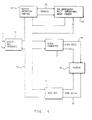
- Fig. 1 is an overall block diagram of a display system according to the present invention.
- Fig. 2 is an illustrative example of the logical placement of bits in an addressable memory array according to the present invention.
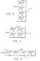
- Fig. 3 is an illustrative example of a memory array having four partition sectors according to the present invention.
- Fig. 4 is another illustrative example of a memory array having four partition sectors according to the present invention.
- Fig. 5 is yet another illustrative example of a memory array having four partition sectors according to the present invention.
- Fig. 6 is a logic diagram of the addressing circuitry associated with the memory array of the present invention.
- Fig. 1 illustrates in functional block form a video display system in which information is input over
system bus 11 tosystem bus interface 12 anddisplay system bus 13.Raster operation control 14 receives such information and generates addresses overaddress bus 15 which are input to bit addressable multidimensional array (BAMDA) 16. Data that is either read out of or written into BAMDA 16 is then provided to display 22 throughvideo formatter 17 viavideo drive 19. Sync generator 18 controls the horizontal and vertical synchronization ofdisplay 22 oversync drive bus 21. The invention disclosed herein is embodied primarily inBAMDA 16. The operation ofraster operation control 14,video formatter 17, sync generator 18, anddisplay 22 is well known in the visual display art and will not be detailed further herein. - Fig..2, which illustrates the logical placement of bits in
BAMDA 16, represents a four-bit wide memory structure but is easily expandable to an n-bit wide memory structure. M0, Ml, M2, and M3 represent four different memory array modules withinBAMDA 16. Each of modules MO-M3 has eight independent addresses and each has an independent write line. The bits inBAMDA 16 are arranged on a diagonal so that all four bits of memory modules MO-M3 are accessed each memory cycle independent of the direction of access. A key concept of the present invention is that the bits inBAMDA 16 may be accessed either horizontally or vertically. - The smallest element in
BAMDA 16 is square matrix 23. The size of square matrix 23 is nxn where n is the number of memory modules inBAMDA 16. In Fig. 2, sinceBAMDA 16 has four memory modules, then the size of matrix 23 is 4x4. Matrix 23 is the smallest repeatable array element contained withinBAMDA 16. - The next biggest element in
BAMDA 16 is apartition sector 24 which comprises several matrices such as matrix 23. The number of bits inpartition sector 24 is equal to the number of bits in a single memory module. Since each memory module has eight independent addresses, the number of bits inpartition sector 24 is equal to 28, or 256 bits. As shown in Fig. 2,partition sector 24 is a 16x16 matrix. The size of a partition sector inBAMDA 16 depends upon the size of the address field in memory modules MO-M3. The 16x16 matrix ofpartition sector 24 is addressed with two 4-bit address fields, that is, there exists a matrix that is 24x24. The number of partition sectors contained withinBAMDA 16 is equal to the number of memory modules contained withinBAMDA 16. Therefore, for an array with four memory modules, there would be four partition sectors. Note that due to space constraints, only one partition sector, that is,partition sector 24, is shown in Fig. 2. - Figs. 3, 4, and 5 depict three different array configurations for
BAMDA 16.Array 25, which comprises partition sectors 26-29, is a 16x64 array.Array 35, which comprises partition sectors 31-34, is a 32x32 bit array.Array 41, which comprises partition sectors 36-39, is a 64x16 bit array. Each of the partition sectors 26-29 inarray 25, partition sectors 31-34 inarray 35, and sectors 36-39 inarray 41, are 16x16 bit in size. A partition select input value represents the number of partition sectors in the X direction. Thus,array 25 has a partition select input value of 1, whilearray 41 has a partition select input value of 4. The partitioning of an array can easily be extended to any array size with any number of memory modules. For example, if the number of memory modules is equal to eight, then the possible partition select input values may be 1, 2, 4, or 8. These four input values would represent array sizes of 1x8, 2x4, 4x2, and 8x1, respectively. - In Fig. 6 is shown the logic necessary to generate the addresses and the write lines for each of modules MO-M3 in
BAMDA 16. A four-bit row and a four-bit column address are generated to each of modules MO-M3 on a common set of multiplexed address lines, 61-66, which are controlled by the rowcolumn strobe input 53. When changing access direction from x to y or vice versa, the row/column address fields are switched by the exclusive OR function embodied ingate 52. The two address inputs shown in Fig. 6 are same direction address (SDA) 42 and opposite direction address (ODA) 43.SDA 42 provides the x direction address when xdirection access input 44 is equal to 1.SDA 42 provides the y direction address when xdirection access input 44 is equal to 0. Likewise,ODA 43 provides the y direction address when xdirection access input 44 is equal to 1, and provides the x direction address when xdirection access 44 is equal to 0. The x,y address presented to BAMDA 16 represents the exact starting bit location regardless of the direction of access. Additionally, the two dimensional x,y address indicates which of memory modules MO-M3 is to be the starting position from which the first bit is accessed. The direction of access has no effect on the module starting position. The module start is generated by adding the two least significant bits of bothSDA 42 andODA 43, and dropping any carry outs that occur during the two-bit add operation. - An
SDA 42 offset value is output frommultiplexor 48. WhenBAMDA 16 is operating in the x directional access mode, the offset value ofSDA 42 is equal to the two most significant bits inODA 43 times the input value of partition select 45. This multiplication takes place in multiplier 46. WhenBAMDA 16 is in the y directional access mode, the offset value ofSDA 42 is equal to the two most significant bits ofODA 43. An offset value forODA 43 is generated in much the same manner as the offset value forSDA 42, except the conditions for choosing the most significant bits versus the least significant bits are switched. The two offset values generated thusly enable the addressing of different partition sectors withinBAMDA 16. Both offset values are equal to 0 when accessingpartition sector 0. The starting bit depicted by the x,y address input will always fall within the partition sector generated by the sum of the offset values ofSDA 42 andODA 43. - The starting position for
SDA 42 is generated by adding the four least significant bits ofSDA 42 to the offset value ofSDA 42. The starting position forODA 43 is generated by adding the four least significant bits ofODA 43 to the offset value ofODA 43. As can be seen in Fig. 6, the SDA starting value is generated byadder 71, while the ODA starting value is generated byadder 72. Only the four least significant bits of theSDA 42 andODA 43 fields are used because each of memory modules MO-M3 has two four-bit wide addresses that are multiplexed into the array modules. These two starting values represent the exact row/column address of the starting bit to be accessed. Together with these start addresses and the module start value, which is generated by two-bit adder 48, the exact starting bit in the proper memory module is accessed. - A module pointer is generated from the module start (output of adder 48) and the module number. For example, a module start value is output from
adder 48 and added withmodule 0 inadder 75 which is then output to one'scomplement 74. The output of one'scomplement 74 is then the module pointer formodule 0. The module pointer represents a sequential string of numbers starting from 0 up to the total number of memory modules inBAMDA 16. There is one and only one module pointer that has a 0 value during a memory access. The module pointer that has this value of 0 also points to the one of memory modules MO-M3 where the starting bit is located. For example, if memory module M2 has the starting bit in it, then memory module M3 has the next consecutive bit in it. Similarly, memory module MO has the third consecutive bit in it. When starting with memory module M2, the module pointer for that M2 is equal to 0. Subsequently, the module pointer value formemory module 3 has a value of 3, the next memory module which is MO then uses a module pointer value of 0 to generate its addresses. The values of such module pointers supply the sequential offsets to generate the sequential address and also the appropriate starting point in the memory modules. - When accessing a four-bit string in the x- direction, there are only two unique row addresses required, the starting address and the starting address plus one. These two addresses are represented by the
ODA 43 start value, which is output fromadder 72, and theODA 43 next value, which is output fromadder 76. TheODA 43 next value is generated by adding the ODA starting value output fromadder 72 to one whenBAMDA 16 is in the x-directional access mode. - The column address field remains constant within a partition sector when accessing in the y direction. Therefore, when accessing a four-bit string in the y direction, there are only two unique column addresses needed for the four memory modules, MO-M3. These two unique column addresses are the starting address and the starting address plus the partition select value. The start address and the start address plus partition select value are represented by the ODA start value and the ODA next value when operating in the y directional access mode. The ODA next value is generated by adding the ODA start value to the partition select value when in this y directional access mode. For accesses to BAMDA 16 that are contained in a given partition sector, the ODA next address is not used. For accesses that cross partition sector boundaries, both the ODA and the ODA next values are used.
- The selection of which one of
ODA 43 addresses is to be used for each independent memory module is generated by the carry select signal for that module. The carry select value, ranging from 0 to 3, is generated from the four least significant bits ofSDA 42 and the module pointer for that module. These two quantities are added together to form a carry bit. For example, formodule 0, the module pointer output from one'scomplement 74 is input to four-bit carrygenerator 81. The other input to carrygenerator 81 is the four least significant bits ofSDA 42. A carry bit is then output fromcarry generator 81 and input to 2:1multiplexor 82. When the carry select signal becomes active, the ODA next value is input to the appropriate memory module. When the carry select signal is inactive, the ODA start value is presented to the appropriate module. This operation frommodule 0 is accomplished by 2:1multiplexor 82. - The column address field and the row address field in
BAMDA 16 are both sequential in nature when going in the x and y directions, respectively. This sequential nature of the address field also applies when crossing the boundaries ofpartition sector 24. In order to generate the proper sequential same direction address to the memory module containing the starting bit, the same direction address starting bit generated at the output ofadder 71 is used. In order to generate the proper sequential same direction address to the second bit in the memory access string, the same direction address starting bit generated at the output ofadder 71 is incremented by one. Consequently, for each consecutive bit in the access string, a new sequential same direction address bit must be generated. The sequential same direction address fields are swapped from row to column address fields and vice versa, depending on the direction of access to BAMDA 16. When accessingBAMDA 16 in the x-direction, the sequential same direction address forms the column addresses. While accessingBAMDA 16 in the y-direction, the sequential same direction address forms the row addresses. Thus, a sequential same direction address bit is generated by adding the same direction address starting bit to the module pointer value of the memory module that is to receive the sequential address. - Write
width input 51 indicates how many bits are to be written intoBAMDA 16. Whenwrite width 51 is set to 0, all bits are written intoBAMDA 16. Whenwrite width 51 is set to 1, all bits except one are written intoBAMDA 16. A write module signal for each of memory modules MO-M3 is generated by writing thewrite width input 51 to the module pointer value for the given memory module. For example, for memory module MO this addition takes place inadder 83, which haswrite width input 51 and the output of one'scomplement 74 as its inputs. Thewrite module 0 signal is then provided over line 84. If a carry condition does not occur from the add operation that takes place inadder 83, then the memory bit is written intoBAMDA 16 over line 84. - While this invention has been particularly shown and described with reference to a preferred embodiment thereof, it will be understood by those skilled in the art that the foregoing and other changes in form and detail may be made therein without departing from the spirit and scope of the invention.
Claims (9)
Applications Claiming Priority (2)
| Application Number | Priority Date | Filing Date | Title |
|---|---|---|---|
| US701328 | 1985-02-13 | ||
| US06/701,328 US4740927A (en) | 1985-02-13 | 1985-02-13 | Bit addressable multidimensional array |
Publications (3)
| Publication Number | Publication Date |
|---|---|
| EP0191280A2 true EP0191280A2 (en) | 1986-08-20 |
| EP0191280A3 EP0191280A3 (en) | 1989-10-18 |
| EP0191280B1 EP0191280B1 (en) | 1993-06-02 |
Family
ID=24816925
Family Applications (1)
| Application Number | Title | Priority Date | Filing Date |
|---|---|---|---|
| EP86100033A Expired - Lifetime EP0191280B1 (en) | 1985-02-13 | 1986-01-02 | Bit adressable multidimensional array |
Country Status (4)
| Country | Link |
|---|---|
| US (1) | US4740927A (en) |
| EP (1) | EP0191280B1 (en) |
| JP (1) | JPH0731489B2 (en) |
| DE (1) | DE3688513T2 (en) |
Cited By (4)
| Publication number | Priority date | Publication date | Assignee | Title |
|---|---|---|---|---|
| GB2193019A (en) * | 1986-07-24 | 1988-01-27 | Gec Avionics | Data storage |
| EP0428327A1 (en) * | 1989-11-14 | 1991-05-22 | Amt(Holdings) Limited | Processor array system |
| GB2245394A (en) * | 1990-06-18 | 1992-01-02 | Rank Cintel Ltd | Video framestore selective addressing system |
| EP0887802A2 (en) * | 1993-08-30 | 1998-12-30 | Xerox Corporation | Method for operating a memory |
Families Citing this family (6)
| Publication number | Priority date | Publication date | Assignee | Title |
|---|---|---|---|---|
| CA1262969A (en) * | 1985-06-25 | 1989-11-14 | Ascii Corporation | Memory system |
| US4864544A (en) * | 1986-03-12 | 1989-09-05 | Advanced Micro Devices, Inc. | A Ram cell having means for controlling a bidirectional shift |
| JPS63163645A (en) * | 1986-12-26 | 1988-07-07 | Ricoh Co Ltd | Two-dimensionally arranged memory device |
| US6604166B1 (en) * | 1998-12-30 | 2003-08-05 | Silicon Automation Systems Limited | Memory architecture for parallel data access along any given dimension of an n-dimensional rectangular data array |
| US7093137B1 (en) * | 1999-09-30 | 2006-08-15 | Casio Computer Co., Ltd. | Database management apparatus and encrypting/decrypting system |
| US11307977B2 (en) * | 2018-09-27 | 2022-04-19 | Intel Corporation | Technologies for direct matrix read and write operations |
Citations (4)
| Publication number | Priority date | Publication date | Assignee | Title |
|---|---|---|---|---|
| US3936664A (en) * | 1973-09-25 | 1976-02-03 | Fuji Xerox Co., Ltd. | Method and apparatus for generating character patterns |
| JPS58103063A (en) * | 1981-12-16 | 1983-06-18 | Hitachi Ltd | Matrix storage device |
| EP0085210A1 (en) * | 1982-01-29 | 1983-08-10 | International Business Machines Corporation | Image processing system |
| JPS58169665A (en) * | 1982-03-31 | 1983-10-06 | Fujitsu Ltd | Vertical-horizontal converting circuit of image array for image memory system |
Family Cites Families (7)
| Publication number | Priority date | Publication date | Assignee | Title |
|---|---|---|---|---|
| US2736880A (en) * | 1951-05-11 | 1956-02-28 | Research Corp | Multicoordinate digital information storage device |
| US3772658A (en) * | 1971-02-05 | 1973-11-13 | Us Army | Electronic memory having a page swapping capability |
| US3763480A (en) * | 1971-10-12 | 1973-10-02 | Rca Corp | Digital and analog data handling devices |
| JPS5216935A (en) * | 1975-07-30 | 1977-02-08 | Hitachi Ltd | Memory system |
| JPS5534790A (en) * | 1978-09-05 | 1980-03-11 | Fuji Photo Film Co Ltd | Ruled line generation method |
| US4249172A (en) * | 1979-09-04 | 1981-02-03 | Honeywell Information Systems Inc. | Row address linking control system for video display terminal |
| DE3015125A1 (en) * | 1980-04-19 | 1981-10-22 | Ibm Deutschland Gmbh, 7000 Stuttgart | DEVICE FOR STORING AND DISPLAYING GRAPHIC INFORMATION |
-
1985
- 1985-02-13 US US06/701,328 patent/US4740927A/en not_active Expired - Lifetime
- 1985-09-24 JP JP60208984A patent/JPH0731489B2/en not_active Expired - Lifetime
-
1986
- 1986-01-02 EP EP86100033A patent/EP0191280B1/en not_active Expired - Lifetime
- 1986-01-02 DE DE86100033T patent/DE3688513T2/en not_active Expired - Lifetime
Patent Citations (4)
| Publication number | Priority date | Publication date | Assignee | Title |
|---|---|---|---|---|
| US3936664A (en) * | 1973-09-25 | 1976-02-03 | Fuji Xerox Co., Ltd. | Method and apparatus for generating character patterns |
| JPS58103063A (en) * | 1981-12-16 | 1983-06-18 | Hitachi Ltd | Matrix storage device |
| EP0085210A1 (en) * | 1982-01-29 | 1983-08-10 | International Business Machines Corporation | Image processing system |
| JPS58169665A (en) * | 1982-03-31 | 1983-10-06 | Fujitsu Ltd | Vertical-horizontal converting circuit of image array for image memory system |
Non-Patent Citations (2)
| Title |
|---|
| PATENT ABSTRACTS OF JAPAN, vol. 7, no. 210 (P-223)[1355], 16th September 1983; & JP-A-58 103 063 (HITACHI SEISAKUSHO K.K.) 18-06-1983 * |
| PATENT ABSTRACTS OF JAPAN, vol. 8, no. 10 (P-248)[1447], 18th January 1984; & JP-A-58 169 665 (FUJITSU K.K.) 06-10-1983 * |
Cited By (5)
| Publication number | Priority date | Publication date | Assignee | Title |
|---|---|---|---|---|
| GB2193019A (en) * | 1986-07-24 | 1988-01-27 | Gec Avionics | Data storage |
| EP0428327A1 (en) * | 1989-11-14 | 1991-05-22 | Amt(Holdings) Limited | Processor array system |
| GB2245394A (en) * | 1990-06-18 | 1992-01-02 | Rank Cintel Ltd | Video framestore selective addressing system |
| EP0887802A2 (en) * | 1993-08-30 | 1998-12-30 | Xerox Corporation | Method for operating a memory |
| EP0887802A3 (en) * | 1993-08-30 | 1999-02-10 | Xerox Corporation | Method for operating a memory |
Also Published As
| Publication number | Publication date |
|---|---|
| US4740927A (en) | 1988-04-26 |
| JPS61186991A (en) | 1986-08-20 |
| EP0191280A3 (en) | 1989-10-18 |
| EP0191280B1 (en) | 1993-06-02 |
| DE3688513D1 (en) | 1993-07-08 |
| DE3688513T2 (en) | 1993-12-23 |
| JPH0731489B2 (en) | 1995-04-10 |
Similar Documents
| Publication | Publication Date | Title |
|---|---|---|
| EP0492939B1 (en) | Method and apparatus for arranging access of VRAM to provide accelerated writing of vertical lines to an output display | |
| US5233689A (en) | Methods and apparatus for maximizing column address coherency for serial and random port accesses to a dual port ram array | |
| US5442748A (en) | Architecture of output switching circuitry for frame buffer | |
| EP0398510B1 (en) | Video random access memory | |
| US4745407A (en) | Memory organization apparatus and method | |
| EP0492938A2 (en) | Method and apparatus for increasing the speed of operation of a double buffered display system | |
| US4903217A (en) | Frame buffer architecture capable of accessing a pixel aligned M by N array of pixels on the screen of an attached monitor | |
| US4670752A (en) | Hard-wired circuit for handling screen windows | |
| US4740927A (en) | Bit addressable multidimensional array | |
| US4876663A (en) | Display interface system using buffered VDRAMs and plural shift registers for data rate control between data source and display | |
| US4870491A (en) | Display control apparatus for supplying display data to raster scanning type display device | |
| EP0525986A2 (en) | Apparatus for fast copying between frame buffers in a double buffered output display system | |
| EP0431581A2 (en) | Method and apparatus for changing the orientation of a video display | |
| US5412740A (en) | Signal processing system having reduced memory space | |
| US5870085A (en) | Generating text strings | |
| US4716546A (en) | Memory organization for vertical and horizontal vectors in a raster scan display system | |
| JPH06167958A (en) | Memory device | |
| US5119331A (en) | Segmented flash write | |
| US4559611A (en) | Mapping and memory hardware for writing horizontal and vertical lines | |
| JPH0740242B2 (en) | Data transfer method | |
| JPH08211849A (en) | Display control device | |
| KR20000018627A (en) | Semiconductor memory device having high multi-bit degree of freedom | |
| JP2708841B2 (en) | Writing method of bitmap memory | |
| JPS63250689A (en) | Raster scan display system | |
| JP2633251B2 (en) | Image memory device |
Legal Events
| Date | Code | Title | Description |
|---|---|---|---|
| PUAI | Public reference made under article 153(3) epc to a published international application that has entered the european phase |
Free format text: ORIGINAL CODE: 0009012 |
|
| AK | Designated contracting states |
Kind code of ref document: A2 Designated state(s): DE FR GB IT |
|
| 17P | Request for examination filed |
Effective date: 19861212 |
|
| PUAL | Search report despatched |
Free format text: ORIGINAL CODE: 0009013 |
|
| AK | Designated contracting states |
Kind code of ref document: A3 Designated state(s): DE FR GB IT |
|
| 17Q | First examination report despatched |
Effective date: 19910412 |
|
| GRAA | (expected) grant |
Free format text: ORIGINAL CODE: 0009210 |
|
| AK | Designated contracting states |
Kind code of ref document: B1 Designated state(s): DE FR GB IT |
|
| REF | Corresponds to: |
Ref document number: 3688513 Country of ref document: DE Date of ref document: 19930708 |
|
| ITF | It: translation for a ep patent filed |
Owner name: IBM - DR. ING. FABRIZIO LETTIERI |
|
| ET | Fr: translation filed | ||
| PLBE | No opposition filed within time limit |
Free format text: ORIGINAL CODE: 0009261 |
|
| STAA | Information on the status of an ep patent application or granted ep patent |
Free format text: STATUS: NO OPPOSITION FILED WITHIN TIME LIMIT |
|
| 26N | No opposition filed | ||
| REG | Reference to a national code |
Ref country code: GB Ref legal event code: IF02 |
|
| PGFP | Annual fee paid to national office [announced via postgrant information from national office to epo] |
Ref country code: DE Payment date: 20041213 Year of fee payment: 20 |
|
| PGFP | Annual fee paid to national office [announced via postgrant information from national office to epo] |
Ref country code: GB Payment date: 20050104 Year of fee payment: 20 |
|
| PGFP | Annual fee paid to national office [announced via postgrant information from national office to epo] |
Ref country code: FR Payment date: 20050124 Year of fee payment: 20 |
|
| PGFP | Annual fee paid to national office [announced via postgrant information from national office to epo] |
Ref country code: IT Payment date: 20050128 Year of fee payment: 20 |
|
| PG25 | Lapsed in a contracting state [announced via postgrant information from national office to epo] |
Ref country code: GB Free format text: LAPSE BECAUSE OF EXPIRATION OF PROTECTION Effective date: 20060101 |
|
| REG | Reference to a national code |
Ref country code: GB Ref legal event code: PE20 |