EP0146513A2 - Current source for arc welding - Google Patents
Current source for arc welding Download PDFInfo
- Publication number
- EP0146513A2 EP0146513A2 EP84850364A EP84850364A EP0146513A2 EP 0146513 A2 EP0146513 A2 EP 0146513A2 EP 84850364 A EP84850364 A EP 84850364A EP 84850364 A EP84850364 A EP 84850364A EP 0146513 A2 EP0146513 A2 EP 0146513A2
- Authority
- EP
- European Patent Office
- Prior art keywords
- voltage
- welding
- inverters
- current source
- inverter
- Prior art date
- Legal status (The legal status is an assumption and is not a legal conclusion. Google has not performed a legal analysis and makes no representation as to the accuracy of the status listed.)
- Withdrawn
Links
Images
Classifications
-
- B—PERFORMING OPERATIONS; TRANSPORTING
- B23—MACHINE TOOLS; METAL-WORKING NOT OTHERWISE PROVIDED FOR
- B23K—SOLDERING OR UNSOLDERING; WELDING; CLADDING OR PLATING BY SOLDERING OR WELDING; CUTTING BY APPLYING HEAT LOCALLY, e.g. FLAME CUTTING; WORKING BY LASER BEAM
- B23K9/00—Arc welding or cutting
- B23K9/10—Other electric circuits therefor; Protective circuits; Remote controls
- B23K9/1006—Power supply
-
- B—PERFORMING OPERATIONS; TRANSPORTING
- B23—MACHINE TOOLS; METAL-WORKING NOT OTHERWISE PROVIDED FOR
- B23K—SOLDERING OR UNSOLDERING; WELDING; CLADDING OR PLATING BY SOLDERING OR WELDING; CUTTING BY APPLYING HEAT LOCALLY, e.g. FLAME CUTTING; WORKING BY LASER BEAM
- B23K9/00—Arc welding or cutting
- B23K9/06—Arrangements or circuits for starting the arc, e.g. by generating ignition voltage, or for stabilising the arc
-
- H—ELECTRICITY
- H02—GENERATION; CONVERSION OR DISTRIBUTION OF ELECTRIC POWER
- H02J—CIRCUIT ARRANGEMENTS OR SYSTEMS FOR SUPPLYING OR DISTRIBUTING ELECTRIC POWER; SYSTEMS FOR STORING ELECTRIC ENERGY
- H02J1/00—Circuit arrangements for dc mains or dc distribution networks
- H02J1/10—Parallel operation of dc sources
- H02J1/102—Parallel operation of dc sources being switching converters
-
- H—ELECTRICITY
- H02—GENERATION; CONVERSION OR DISTRIBUTION OF ELECTRIC POWER
- H02J—CIRCUIT ARRANGEMENTS OR SYSTEMS FOR SUPPLYING OR DISTRIBUTING ELECTRIC POWER; SYSTEMS FOR STORING ELECTRIC ENERGY
- H02J1/00—Circuit arrangements for dc mains or dc distribution networks
- H02J1/10—Parallel operation of dc sources
- H02J1/108—Parallel operation of dc sources using diodes blocking reverse current flow
Definitions
- the invention relates to a welding current source for arc welding with a rectifier that can be connected to an AC network, a parallel circuit connected to its DC terminals, consisting of a smoothing capacitor device and an inverter device for converting the DC voltage into an AC voltage, the frequency of which is significantly higher than the mains frequency, whereby the inverter device is equipped with semiconductor elements which are controlled by a control unit and is equipped with a transformer device for the galvanic isolation of the input of the inverter device from its output, to which, after an optional series connection of a rectifier, a welding point formed from a workpiece and a welding electrode can be connected.
- Welding current sources are usually equipped with a transformer for reducing the mains voltage to the lower welding voltage. Thanks to the use of a significantly higher frequency, the size of the transformer is significantly reduced compared to the size of a transformer of the same power for the mains frequency. Frequencies of at least 0.5 kHz are understood here as significantly higher frequencies. It is particularly expedient to choose a frequency which is more than 15 kHz and is therefore above the audibility threshold. The higher frequency allows a faster regulation of the welding parameters, in particular the welding current and the welding voltage, compared to the mains frequency. Welding current sources of this type are known for example from US 4 159 409 and GB 2 046 535.
- controllable semiconductor elements for higher frequencies are expensive and in some respects have poorer operating values than corresponding semiconductor elements for normal network frequencies. In particular, these semiconductor elements have poorer characteristic values, which undermines their overload capacity through compensating processes, e.g. rapid current and voltage changes. Such semiconductor elements for normal line voltages are particularly expensive.
- mains voltage of 380 V the smoothed DC voltage is approximately 530 V. Since the dimensioning of the semiconductor elements also has to take into account the fluctuation in the mains voltage and compensation processes, it is necessary to design the semiconductor elements for approximately 600 V at a mains voltage of 380 V and for approximately 800 V at a mains voltage of 500 V.
- the present invention has therefore set itself the task of a cheap welding power source with change richter to create, in which these less expensive semiconductor elements can be used at common line voltages.
- the solution to this problem is that the inverter device consists of two or more inverters, the inputs of which are connected in series, and that the smoothing capacitor device serves as a voltage divider that consists of two or more capacitors connected in series, with connections arranged between the capacitors with corresponding connections are connected between the inverters connected in series.
- Each inverter is therefore only a part of the total voltage and it is therefore possible to use semiconductor elements which are only to be designed for these partial voltages.
- the inputs of two inverters of the same type are connected in series and control devices of the two inverters are provided for controlling the semiconductor elements for alternately generating voltage pulses at the outputs of the two inverters, a circuit consisting of between each output and the welding point a series connection of rectifier and welding inductor and one with the Welding inductor interacting free-wheeling diode is switched on.
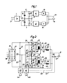
- a rectifier 1 is connected to a single-phase network 2.
- Two to a line 3 in series g esch ALTENE inverters 4, 5 are connected to lines 6, 7 to the rectifier. 1
- the inverters are equipped with controllable semiconductor elements. Inverter circuits of this type are generally known.
- the semiconductor elements can be thyristors and transistors.
- the frequency of the AC voltage output by the inverters 4, 5 is preferably 15 kHz or higher.
- the AC voltage is rectified in the corresponding rectifier 13, 14 and fed to a welding point consisting of electrode 15 and workpiece 16.
- the resistors 10, 11 are the same size and the voltage across each of the two inverters is therefore also approximately the same size. Slight deviations from these voltage values occur due to the charging and discharging of the capacitors taking place in time with the inverter frequency.
- FIG. 2 shows a three-phase rectifier 17 which is connected to a three-phase network 18.
- Two smoothing capacitors 21, 22 connected in series and two inverters 23, 24 connected in series with their inputs 25, 26, 27, 28 are connected to the output 19, 20 of the rectifier.
- the inputs 26, 27 are connected by a terminal 29 which is connected to a terminal 30 of the connecting line of the two capacitors 21, 22.
- the outputs 31, 32, 33, 34 of the inverters are connected in series with one diode 35, 36 and one welding inductor 37, 38 each.
- a free-wheeling diode 39, 40 for each output takes over the welding current when the energy flow is interrupted by the inverter.
- the two output circuits 35, 37, 39 and 36, 38, 40 are connected in parallel and connected to a welding electrode 41 and a workpiece 42.
- the circuit of the two inverters 23, 24 is identical and therefore only one of the two inverters is described in more detail.
- the parts of the inverters 23, 24 are provided with the same reference symbols.
- the inverter 23 is an asymmetrical half-bridge inverter. Two in parallel Circles each contain a diode 43, 44 and a semiconductor element 46, 47 which can be controlled by a control device 45.
- MOS field effect transistors also called Mosfet for short, are used as semiconductor elements which, in contrast to the normal bipolar transistors, are controlled practically without power will.
- the mosfet has a positive temperature coefficient, i.e. its resistance increases with increasing temperature.
- the Mosfet can therefore be connected in parallel without special switching elements or auxiliary circuits, the current being distributed over the Mosfets connected in parallel in the ratio of the resistances. Due to the positive temperature coefficient, overloads in the Mosfet cannot cause an uncontrollable increase in current, since local heating in the overloaded area of the Mosfet leads to a corresponding decrease in current.
- the Mosfet thus has several advantages over the bipolar transistor.
- a disadvantage is the low dielectric strength.
- Mosfets with blocking voltages up to 800 V are currently available.
- these mosfets are expensive, especially for the high currents for which welding current sources have to be dimensioned. It is therefore understandable that the use of cheap mosfets with low dielectric strength is desirable.
- the primary winding 49 of a transformer 48 is connected between the two MOSFETs.
- Resistors 51, 52 are connected between one connection of transformer 48 and the two connections 25, 29.
- the secondary winding 50 of the transformer is connected directly to the output 31, 32 of the inverter.
- the resistors 51, 52 in the two inverters act in the same way as described above for the resistors 10, 11 in FIG. 1.
- the DC voltage of the rectifier 17 is divided into two equal partial voltages between the terminals 25, 29 and 29, 28 by the two pairs of resistors 51, 52, which have the same resistance.
- the potential of the connection points 29, 30 is therefore theoretically between the two potentials of the rectifier outputs 19, 20.
- slight fluctuations in the potential of the connection points 29, 30 are caused, for example, by different pulse lengths of the control signals to the Mosfets and by different charge and discharge currents of the capacitors .
- the Mosfets of the two inverters 23, 24 are thus only exposed to half the operating DC voltage occurring between the terminals 25, 29 and 29, 28 plus a small surcharge for the potential fluctuations occurring in the terminal 29.
- the potential of the terminal 29 can deviate greatly from its operating value, as a result of which the voltage at one of the inverters can be increased such that the Mosfets are exposed to a destructive surge.
- the occurrence of such an overvoltage on the mosfet is avoided with the help of a monitoring circuit.
- the voltage of the capacitor 22 is compared in a comparator 53 with a voltage set by means of an actuator 54. If the difference between the capacitor voltage and the set voltage exceeds a certain value, the comparator 53 emits a signal to the control device, which immediately blocks the MOSFET 46, 47 via the control lines 55.
- each Mosfet is therefore only loaded with about a quarter of the DC voltage between the output terminals 19, 20 as long as the capacitors are free of defects.
- the voltage between the terminals 19, 20 is divided between the two capacitors in the inverse proportion to their capacitance. Since the mass-produced capacitors available on the market have capacitance values that can deviate significantly from their nominal value within the permissible tolerances, it can be expected that the inverters will not be at the same instant, as intended, but at very different partial voltages. After a short time, however, the partial voltages will set to a value which is determined by the resistors 51, 52 in the inverters 23, 24. The surge voltages at the moment of switching on can damage the Mosfets. It would now be possible to select suitable capacitors with the same capacitance values, but this incurs additional costs.
- the voltage of the capacitor 22 is running from the comparator If an overvoltage is monitored on one of the two capacitors 21, 22, the difference between the voltage of the capacitor 22 and the voltage set on the actuator 54 of the comparator exceeds a predetermined value. A corresponding output signal from the comparator 53 to the control unit 45 leads to an immediate blocking of the Mosfets.
- the voltage across a MOSFET can therefore in the worst case - if, for example, one of the two capacitors 21, 22 is defective and short-circuited - make up at most half the voltage between the terminals 19, 20, since, as assumed above, the resistors 51, 52 are the same are big.
- a voltage corresponding to the welding current is tapped at a shunt 56, which voltage is fed together with the welding voltage via lines 51, 58, 59 to the control device 45 common to both inverters.
- An actuator 60 is provided on the control device for setting the setpoint value of welding current and / or welding voltage. In contrast to the illustration shown here, it is also conceivable to provide each inverter with its own control unit.
- the two inverters 23, 24 are expediently operated by the control device as pulse-width-modulated inverters in push-pull mode.
- the inverters emit alternating voltage pulses of a certain length at their outputs 31, 32 and 33, 34. If the inverters are loaded in this way, it has proven to be advantageous to use the inverters 23, 24 with their rectifiers 35, 36, their welding inductors 37, 38 and each to connect their freewheeling diode 39, 40 before the two inverters are connected in parallel and connected to the common welding point 41, 42.
Landscapes
- Engineering & Computer Science (AREA)
- Physics & Mathematics (AREA)
- Plasma & Fusion (AREA)
- Mechanical Engineering (AREA)
- Power Engineering (AREA)
- Arc Welding Control (AREA)
- Inverter Devices (AREA)
- Arc Welding In General (AREA)
Abstract
Eine Schweissstromquelle für das Lichtbogenschweissen ist über einen Gleichrichter (1) an ein Wechselstromnetz angeschlossen. An die Gleichspannungsklemmen ist eine Glättungskondensatoreinrichtung (8, 9) und eine Wechselrichtereinrichtung angeschlossen, in der die Gleichspannung in eine Wechselspannung mit höherer Frequenz, von beispielsweise über 15 kHz, umgewandelt wird. Die Wechselrichtereinrichtung besteht aus mehreren einzelnen Wechselrichtern (4, 5), deren Eingänge in Serie geschaltet sind. Die Glättungskondensatoreinrichtung besteht aus zwei oder mehreren in Serie geschaltenen Kondensatoren (8, 9) und dient als Spannungsteiler. Die zwischen den Kondensatoren angeordneten Anschlüsse (12) sind mit entsprechenden Anschlüssen (3) zwischen den in Serie geschaltenen Wechselrichtern (4, 5) verbunden. Die parallelgeschalteten Ausgänge der Wechselrichter sind an eine Schweissstelle (15, 16) angeschlossen.
Description
Die Erfindung bezieht sich auf eine Schweissstromquelle für das Lichtbogenschweissen mit einem an ein Wechselstromnetz anschliessbaren Gleichrichter, einer an dessen Gleichstromklemmen angeschlossenen Parallelschaltung bestehend aus einer Glättungskondensatoreinrichtung und einer Wechselrichtereinrichtung für die Umwandlung der Gleichspannung in eine Wechselspannung,deren Frequenz wesentlich höher als die Netzfrequenz ist, wobei die Wechselrichtereinrichtung mit Halbleiterelementen, die von einem Steuergerät gesteuert werden, und mit einer Transformatoreinrichtung für die galvanische Trennung des Einganges der Wechselrichtereinrichtung von ihrem Ausgang ausgerüstet ist, an den nach fakultativer Serienschaltung eines Gleichrichters eine aus einem Werkstück und einer Schweisselektrode gebildete Schweissstelle anschliessbar ist.The invention relates to a welding current source for arc welding with a rectifier that can be connected to an AC network, a parallel circuit connected to its DC terminals, consisting of a smoothing capacitor device and an inverter device for converting the DC voltage into an AC voltage, the frequency of which is significantly higher than the mains frequency, whereby the inverter device is equipped with semiconductor elements which are controlled by a control unit and is equipped with a transformer device for the galvanic isolation of the input of the inverter device from its output, to which, after an optional series connection of a rectifier, a welding point formed from a workpiece and a welding electrode can be connected.
Schweissstromquellen sind üblicherweise mit einem Transformator für die Herabsetzung der Netzspannung auf die geringere Schweissspannung ausgerüstet. Dank der Verwendung einer wesentlich höheren Frequenz wird die Baugrösse des Transformators im Vergleich zu der Baugrösse eines Transformators gleicher Leistung für Netzfrequenz wesentlich verringert. Als wesentlich höhere Frequenzen werden hier Frequenzen von mindestens 0,5 kHz verstanden. Es ist besonders zweckmässig eine Frequenz zu wählen, die mehr als 15 kHz beträgt und somit über der Hörbarkeitsschwelle liegt. Die höhere Frequenz gestattet im Vergleich zur Netzfrequenz eine raschere Regelung der Schweissparameter, insbesondere von Schweissstrom und Schweissspannung. Schweissstromquellen dieser Gattung sind beispielsweise durch US 4 159 409 und GB 2 046 535 bekannt geworden.Welding current sources are usually equipped with a transformer for reducing the mains voltage to the lower welding voltage. Thanks to the use of a significantly higher frequency, the size of the transformer is significantly reduced compared to the size of a transformer of the same power for the mains frequency. Frequencies of at least 0.5 kHz are understood here as significantly higher frequencies. It is particularly expedient to choose a frequency which is more than 15 kHz and is therefore above the audibility threshold. The higher frequency allows a faster regulation of the welding parameters, in particular the welding current and the welding voltage, compared to the mains frequency. Welding current sources of this type are known for example from US 4 159 409 and GB 2 046 535.
Die Verwendung einer höheren Frequenz bringt allerdings auch Nachteile mit sich. Die steuerbaren Halbleiterelemente für höhere Frequenzen sind teuer und haben in mancher Beziehung schlechtere Betriebswerte als entsprechende Halbleiterelemente für normale Netzfrequenzen. Insbesondere haben diese Halbleiterelemente schlechtere Kennwerte, was ihre Überlastungsfähigkeit durch Ausgleichsvorgänge, z.B. rasche Strom- und Spannungsänderungen, betrifft. Derartige Halbleiterelemente für normale Netzspannungen sind besonders teuer. Es ist dabei zu beachten, dass bei einer Netzwechselspannung von 380 V die geglättete Gleichspannung etwa 530 V beträgt. Da man bei der Dimensionierung der Halbleiterelemente auch auf die Schwankung der Netzspannung und auf Ausgleichsvorgänge Rücksicht nehmen muss, ist es erforderlich bei einer Netzspannung von 380 V die Halbleiterelemente für etwa 600 V und bei einer Netzspannung von 500 V für etwa 800 V auszulegen.However, the use of a higher frequency also has disadvantages. The controllable semiconductor elements for higher frequencies are expensive and in some respects have poorer operating values than corresponding semiconductor elements for normal network frequencies. In particular, these semiconductor elements have poorer characteristic values, which undermines their overload capacity through compensating processes, e.g. rapid current and voltage changes. Such semiconductor elements for normal line voltages are particularly expensive. It should be noted that with a mains voltage of 380 V the smoothed DC voltage is approximately 530 V. Since the dimensioning of the semiconductor elements also has to take into account the fluctuation in the mains voltage and compensation processes, it is necessary to design the semiconductor elements for approximately 600 V at a mains voltage of 380 V and for approximately 800 V at a mains voltage of 500 V.
Insbesondere bei kleineren Schweissstromquellen, die in grossen Serien hergestellt werden, beeinflussen die Kosten der Halbleiterelemente für diese hohen Spannungen wesentlich den Gesamtpreis der Stromquelle. Es war daher besonders wünschenswert eine Stromquelle zu entwickeln, für die bei gleicher Netzspannung die billigeren Halbleiterelemente für niedrigere Betriebsspannungen verwendet können. Die weitere Entwicklung der Halbleiterelemente wird in der Zukunft wohl zu einer Verbilligung der Halbleiterelemente für hohe Spannungen führen. Es ist aber zu erwarten, dass sich das Preisverhältnis zwischen Halbleiterelementenfür hohe und für niedrige Spannungen kaum ändern wird und somit die Halbleiterelemente für niedrige Spannungen auch weiterhin preislich wesentlich vorteilhafter sein werden.Particularly in the case of smaller welding current sources which are produced in large series, the costs of the semiconductor elements for these high voltages have a significant influence on the total price of the current source. It was therefore particularly desirable to develop a current source for which the cheaper semiconductor elements for lower operating voltages can be used for the same mains voltage. The further development of semiconductor elements in the future will probably lead to cheaper semiconductor elements for high voltages. However, it is to be expected that the price ratio between semiconductor elements for high and for low voltages will hardly change, and thus the semiconductor elements for low voltages will continue to be significantly more advantageous in terms of price.
Die vorliegende Erfindung hat sich somit zur Aufgabe gestellt eine billige Schweissstromquelle mit Wechselrichter zu schaffen, bei der diese preisgünstigeren Halbleiterelemente bei üblichen Netzspannungen verwendet werden könnne. Die Lösung dieser Aufgabe besteht darin, dass die Wechselrichtereinrichtung aus zwei oder mehreren Wechselrichtern besteht, deren Eingänge in Serie geschaltet sind, und dass die Glättungskondensatoreinrichtung als Spannungsteiler dient, der aus zwei oder mehreren in Serie geschalteten Kondensatoren besteht, wobei zwischen den Kondensatoren angeordnete Anschlüssen mit entsprechenden Anschlüssen zwischen den in Serie geschalteten Wechselrichtern verbunden sind. Jeder Wechselrichter liegt daher nur an einem Teil der Gesamtspannung und es können daher Halbleiterelemente verwendet werden, die lediglich für diese Teilspannungen auszulegen sind.The present invention has therefore set itself the task of a cheap welding power source with change richter to create, in which these less expensive semiconductor elements can be used at common line voltages. The solution to this problem is that the inverter device consists of two or more inverters, the inputs of which are connected in series, and that the smoothing capacitor device serves as a voltage divider that consists of two or more capacitors connected in series, with connections arranged between the capacitors with corresponding connections are connected between the inverters connected in series. Each inverter is therefore only a part of the total voltage and it is therefore possible to use semiconductor elements which are only to be designed for these partial voltages.
Es ist zweckmässig die Gesamtspannung durch den Spannungsteiler gleichmässig auf die in Serie geschalteten Wechselrichter aufzuteilen. Diese Aufteilung der Spannung wird allerdings im Leerlauf gestört, wenn die Magnetisierungsströme der Transformatoren ungleich sind. In ähnlicher Weise wird die gewünschte Aufteilung der Spannung auch durch unterschiedliche Leckströme der Kondensatoren nachteilig beeinflusst. Dieser Störung wird gemäss der Ausführungsform der Erfindung dadurch abgeholfen, dass jedem Glättungskondensator ein Widerstand parallel geschaltet ist. Die Aufteilung der Spannung richtet sich im Leerlauf im wesentlichen nach der Grösse der Widerstände.It is advisable to distribute the total voltage evenly across the series connected inverters through the voltage divider. This distribution of the voltage is disturbed in no-load operation if the magnetizing currents of the transformers are unequal. Similarly, the desired distribution of the voltage is also adversely affected by different leakage currents of the capacitors. According to the embodiment of the invention, this disturbance is remedied in that a resistor is connected in parallel to each smoothing capacitor. The distribution of the voltage in idle depends essentially on the size of the resistors.
Gemäss einer weiteren vorteilhaften Ausführungsform der Erfindung sind die Eingänge von zwei gleichartigen Wechselrichtern in Serie geschaltet und Steuergeräte der beiden Wechselrichter für die Steuerung der Halbleiterelemente zur wechselweisenErzeugung von Spannungspulsen an den Ausgängen der beiden Wechselrichter vorgesehen, wobei zwischen jedem Ausgang und der Schweissstelle ein Stromkreis bestehend aus einer Serienschaltung von Gleichrichter und Schweissinduktor und einer mit dem Schweissinduktor zusammenwirkenden Freilaufdiode eingeschaltet ist.According to a further advantageous embodiment of the invention, the inputs of two inverters of the same type are connected in series and control devices of the two inverters are provided for controlling the semiconductor elements for alternately generating voltage pulses at the outputs of the two inverters, a circuit consisting of between each output and the welding point a series connection of rectifier and welding inductor and one with the Welding inductor interacting free-wheeling diode is switched on.
Es hat sich gezeigt, dass ein Anschluss der beiden Wechselrichter an einen gemeinsamen Schweissinduktor bei ungleichen Steuerpulsen an die Halbleiterelemente der Wechselrichter zu einer Instabilität des Potentiales der Verbindungsklemme zwischen den beiden seriengeschalteten Wechselrichtern führt, was eine ungleiche Spannungsverteilung auf die beiden Wechselrichter und eine unerwünschte Spannungsbelastung zur Folge hat. Wenn an die Ausgänge der beiden Wechselrichter je ein Schweissinduktor in Serie geschaltet wird, tritt diese Instabilität nicht auf.It has been shown that connecting the two inverters to a common welding inductor with unequal control pulses to the semiconductor elements of the inverters leads to instability in the potential of the connecting terminal between the two series-connected inverters, which leads to an uneven voltage distribution between the two inverters and an undesirable voltage load Consequence. If a welding inductor is connected in series to the outputs of the two inverters, this instability does not occur.
Weitere Vorteile der Erfindung sind der nachfolgenden Beschreibung einer Ausführungsform der Erfindung im Zusammenhang mit der beigefügten Zeichnung zu entnehmen.
- Fig. 1 zeigt etwas schematisch das Schaltbild einer Stromquelle.
- Fig. 2 ist ein detailliertes und etwas modifiziertes Schaltbild der Stromquelle.
- Fig. 1 shows somewhat schematically the circuit diagram of a current source.
- Figure 2 is a detailed and somewhat modified circuit diagram of the current source.
Ein Gleichrichter 1 ist an ein Einphasennetz 2 angeschlossen. Zwei mit einer Leitung 3 in Serie geschaltene Wechselrichter 4, 5 sind mit Leitungen 6, 7 an den Gleichrichter 1 angeschlossen. Die Wechselrichter sind mit steuerbaren Halbleiterelementen ausgerüstet. Wechselrichterschaltungen dieser Art sind allgemein bekannt. Die Halbleiterelemente können Thyristoren und Transistoren sein.A rectifier 1 is connected to a single-phase network 2. Two to a line 3 in series g esch ALTENE
Zwei in Serie geschaltene Glättungskondensatoren 8, 9 und mit diesen parallelgeschaltene Widerstände 10, 11 sind mit den Leitungen 6, 7 verbunden. Die Klemme 12 zwischen den Kondensatoren 8, 9 ist an die Leitung 3 angeschlossen.Two
Die Frequenz der von den Wechselrichtern 4, 5 abgegebenen Wechselspannung ist vorzugsweise 15 kHz oder höher. Die Wechselspannung wird in den entsprechenden Gleichrichter 13, 14 gleichgerichtet und einer aus Elektrode 15 und Werkstück 16 bestehenden Schweissstelle zugeführt. Die Widerstände 10, 11 sind gleich gross und die Spannung über jeden der beiden Wechselrichter ist daher auch ungefähr gleich gross. Geringfügige Abweichungen von diesen Spannungswerten treten auf wegen der im Takt mit der Wechselrichterfrequenz stattfindenden Ladung und Entladung der Kondensatoren.The frequency of the AC voltage output by the
In Fig. 2 ist ein Dreiphasengleichrichter 17 dargestellt, der an ein Dreiphasennetz 18 angeschlossen ist. An den Ausgang 19, 20 des Gleichrichters sind zwei in Serie geschaltene Glättungskondensatoren 21, 22 und zwei mit ihren Eingängen 25, 26, 27, 28 in Serie geschaltene Wechselrichter 23, 24 angeschlossen. Die Eingänge 26, 27 sind durch eine Klemme 29 verbunden, die mit einer Klemme 30 der Verbindungsleitung der beiden Kondensatoren 21, 22 verbunden ist.2 shows a three-phase rectifier 17 which is connected to a three-phase network 18. Two
Die Ausgänge 31, 32, 33, 34 der Wechselrichter sind mit je einer Diode 35, 36 und je einem Schweissinduktor 37, 38 in Serie geschaltet. Eine Freilaufdiode 39, 40 je Ausgang übernimmt den Schweissstrom, wenn der Energiefluss vom Wechselrichter unterbrochen wird. Die beiden Ausgangskreise 35, 37, 39 bzw. 36, 38, 40 sind parallel geschaltet und an eine Schweisselektrode 41 und ein Werkstück 42 angeschlossen.The
Die Schaltung der beiden Wechselrichter 23, 24 ist identisch und es wird daher nur einer der beiden Wechselrichter näher beschrieben. Die Teile der Wechselrichter 23, 24 sind mit den gleichen Bezugszeichen versehen. Der Wechselrichter 23 ist ein asymmetricher Halbbrückenwechselrichter. Zwei parallele Kreise enthalten je eine Diode 43, 44 und je ein von einem Steuergerät 45 steuerbares Halbleiterelement 46, 47. In der vorliegenden Schaltung werden MOS-Feldeffekttransistoren, auch kurz Mosfet genannt, als Halbleiterelemente verwendet, die im Gegensatz zu den normalen bipolaren Transistoren praktisch leistüngslos gesteuert werden.The circuit of the two
Der Mosfet besitzt einen positiven Temperaturkoeffizienten, d.h. sein Widerstand steigt mit zunehmender Temperatur. Der Mosfet kann daher, im Gegensatz zum bipolaren Transistor, ohne besondere Schaltelemente oder Hilfskreise parallel geschaltet werden, wobei sich der Strom im Verhältnis der Widerstände auf die parallelgeschaltenen Mosfets verteilt. Wegen des positiven Temperaturkoeffizienten können Überlastungen im Mosfet keine unkontrollierbare Stromzunahme verursachen, da lokale Erwärmungen im überlasteten Bereich des Mosfet zu einer entsprechenden Stromabnahme führen.The mosfet has a positive temperature coefficient, i.e. its resistance increases with increasing temperature. In contrast to the bipolar transistor, the Mosfet can therefore be connected in parallel without special switching elements or auxiliary circuits, the current being distributed over the Mosfets connected in parallel in the ratio of the resistances. Due to the positive temperature coefficient, overloads in the Mosfet cannot cause an uncontrollable increase in current, since local heating in the overloaded area of the Mosfet leads to a corresponding decrease in current.
Bei den bipolaren Transistoren besteht die Gefahr einer solchen unkontrollierbaren Stromzunahme, da die bipolaren Transistoren einen negativen Temperaturkoeffizienten aufweisen. Der Mosfet besitzt somit gegenüber dem bipolaren Transistor einige Vorteile. Ein Nachteil ist jedoch die geringe Spannungsfestigkeit. Derzeit sind wohl Mosfets mit Sperrspannungen bis zu 800 V erhältlich. Diese Mosfets sind jedoch teuer, insbesondere für die hohen Ströme, für die Schweissstromquellen dimensioniert werden müssen. Es ist daher verständlich , dass die Verwendung von billiger Mosfets mit geringer Spannungsfestigkeit erstrebenswert ist.With the bipolar transistors there is a risk of such an uncontrollable increase in current since the bipolar transistors have a negative temperature coefficient. The Mosfet thus has several advantages over the bipolar transistor. A disadvantage is the low dielectric strength. Mosfets with blocking voltages up to 800 V are currently available. However, these mosfets are expensive, especially for the high currents for which welding current sources have to be dimensioned. It is therefore understandable that the use of cheap mosfets with low dielectric strength is desirable.
Im vorliegenden Schaltbild ist lediglich je ein einziger Mosfet 46, 47 in Serie mit seiner Diode 43, 44 dargestellt. Im Hinblick auf die hohen Schweissströme und die oben erwähnte geringe Strombelastbarkeit eines einzelnen Mosfet müssen im allgemeinen mehrere Mosfets parallel geschaltet werden.In the present circuit diagram, only a single Mosfet 46, 47 is shown in series with its
Die Primärwicklung 49 eines Transformators 48 ist zwischen den beiden Mosfet eingeschaltet. Widerstände 51, 52 sind zwischen einem Anschluss des Transformators 48 und den beiden Anschlüssen25, 29 eingeschaltet. Die Sekundärwicklung 50 des Transformators ist direkt mit dem Ausgang 31, 32 des Wechselrichters verbunden. Die Widerstände 51, 52 in den beiden Wechselrichtern wirken in gleicher Weise wie dies oben für die Widerstände 10, 11 in Fig. 1 beschrieben wurde.The
Die Gleichspannung des Gleichrichters 17 wird durch die beiden Widerstandspaare 51, 52, die den gleichen Widerstand haben, in zwei gleiche Teilspannungen zwischen den Klemmen 25, 29 und 29, 28 aufgeteilt. Das Potential der Anschlusspunkte 29, 30 liegt daher theoretisch zwischen den beiden Potentialen der Gleichrichterausgänge 19, 20. Geringfügige Schwankungen des Potentials der Anschlusspunkte 29, 30 werden jedoch beispielsweise durch verschiedene Impulslängen der Steuersignale an die Mosfets und durch unterschiedliche Ladungs- und Entladungsströme der Kondensatoren verursacht. Die Mosfets der beiden Wechselrichter 23, 24 werden somit nur der halben zwischen den Klemmen 25, 29 bzw. 29, 28 auftretenden Betriebsgleichspannung plus einem geringen Zuschlag für die auftretenden Potentialschwankungen der Klemme 29 ausgesetzt.The DC voltage of the rectifier 17 is divided into two equal partial voltages between the
Infolge Fehler durch schadhafte Schaltelemente kann das Potential der Klemme 29 allerdings von seinem Betriebswert stark abweichen, wodurch die Spannung an einem der Wechselrichter derart erhöht werden kann, dass die Mosfets einer zerstörenden Überspannung ausgesetzt werden. Das Auftreten einer solchen Überspannung am Mosfet wird jedoch mit Hilfe eines Uberwachungskreises vermieden. Die Spannung des Kondensators 22 wird in einem Komparator 53 mit einer mittels eines Stellers 54 eingestellten Spannung verglichen. Überschreitet die Differenz zwischen Kondensatorspannung und der eingestellten Spannung einen bestimmten Wert gibt der Komparator 53 ein Signal an das Steuergerätab, das über die Steuerleitungen 55 die Mosfet 46, 47 sofort sperrt. Wenn der Strom durch die Mosfets unterbrochen ist,richtet sich die Aufteilung der Spannung nur nach den Widerständen 51, 52, die hier als gleich gross vorausgesetzt sind. Jeder Mosfet wird daher nur mit etwa einem Viertel der Gleichspannung zwischen den Ausgangsklemmen 19, 20 belastet, soferne die Kondensatoren fehlerfrei sind.As a result of faults due to defective switching elements, the potential of the terminal 29 can deviate greatly from its operating value, as a result of which the voltage at one of the inverters can be increased such that the Mosfets are exposed to a destructive surge. However, the occurrence of such an overvoltage on the mosfet is avoided with the help of a monitoring circuit. The voltage of the
Wenn die unbelastete Schweissstromquelle an die Netzspannung angeschlossen wird, teilt sich im ersten Augenblick die Spannung zwischen den Klemmen 19, 20 auf die beiden Kondensatoren im umgekehrten Verhältnis zu deren Kapazität auf. Da die im Handel erhältlichen massenpröduzierten Kondensatoren Kapazitätswerte aufweisen, die im Rahmen der zulässigen Toleranzen wesentlich von ihrem Nennwert abweichen können, ist zu erwarten, dass die Wechselrichter im Einschaltaugenblick nicht, wie vorgesehen an gleichen, sondern an stark unterschiedlichen Teilspannungen liegen werden. Nach kurzer Zeit werden sich allerdings die Teilspannungen auf einen Wert einstellen der durch die Widerstände 51, 52 in den Wechselrichtern 23, 24 bestimmt ist. Die Überspannungen im Einschaltaugenblick können zu einer Beschädigung der Mosfets führen. Es wäre nun möglich passende Kondensatoren mit gleichen Kapazitätswerten auszuwählen, was jedoch zusätzliche Kosten verursacht.When the unloaded welding current source is connected to the mains voltage, the voltage between the
Da die Spannung des Kondensators 22 vom Komparator laufend überwacht wird führt eine Überspannung an einem der beiden Kondensatoren 21, 22 dazu, dass die Differenz zwischen der Spannung des Kondensators 22 und der am Stellgerät 54 des Komparators eingestellten Spannung einen vorgegebenen Wert überschreitet. Ein entsprechendes Ausgangssignal vom Komparator 53 an das Steuergerät 45 führt zu einer unmittelbaren Sperrung der Mosfets. Die Spannung über einen Mosfet kann somit im ungünstigen Fall - wenn z.B. einer der beiden Kondensatoren 21, 22 schadhaft und kurzgeschlossen ist - höchstens die Hälfte der Spannung zwischen der Klemmen 19, 20 ausmachen, da, wie oben vorausgesetzt, die Widerstände 51, 52 gleich gross sind.Since the voltage of the
Es ist auch denkbar das Potential der Klemme 19 ebenfalls an einen Eingang des Komparators anzuschliessen und in diesem die Spannungen an beiden Kondensatoren 21 mit einer vorgegebenen Spannung zu vergleichen.It is also conceivable to also connect the potential of the terminal 19 to an input of the comparator and to compare the voltages on both
An einem Shunt 56 wird eine dem Schweissstrom entsprechende Spannung abgegriffen, die zusammen mit der Schweissspannung über Leitungen 51, 58, 59 dem für beide Wechselrichter gemeinsammen Steuergerät 45 zugeführt werden. An das Steuergerät ist ein Steller 60 für die Einstellung des Sollwertes von Schweissstrom und/oder Schweissspannung vorgesehen. Im Gegensatz zu der hier gezeigten Darstellung ist es auch denkbar jeden Wechselrichter mit einem eigenen Steuergerät zu versehen.A voltage corresponding to the welding current is tapped at a
Die beiden Wechselrichter 23, 24 werden zweckmässigerweise vom Steuergerät als pulsbreitenmodulierte Wechselrichter, im Gegentakt betrieben. Die Wechselrichter geben dabei an ihren Ausgängen 31, 32 bzw. 33, 34 wechselweise Spannungsimpulse von bestimmter Länge ab. Wenn die Wechelsrichter derart belastet werden, hat es sich als vorteilhaft erwiesen, die Wechselrichter 23, 24 mit je ihrem Gleichrichter 35, 36 je ihrem Schweissinduktor 37, 38 und je ihrer Freilaufdiode 39, 40 zu beschalten, bevor die beiden Wechselrichter parallel geschaltet und an die gemeinsame Schweissstelle 41, 42 angeschlossen werden.The two
Claims (6)
Applications Claiming Priority (2)
| Application Number | Priority Date | Filing Date | Title |
|---|---|---|---|
| SE8306550 | 1983-11-28 | ||
| SE8306550A SE438109B (en) | 1983-11-28 | 1983-11-28 | STROMKELLA FOR LIGHT REAR WELDING |
Publications (2)
| Publication Number | Publication Date |
|---|---|
| EP0146513A2 true EP0146513A2 (en) | 1985-06-26 |
| EP0146513A3 EP0146513A3 (en) | 1987-12-02 |
Family
ID=20353488
Family Applications (1)
| Application Number | Title | Priority Date | Filing Date |
|---|---|---|---|
| EP84850364A Withdrawn EP0146513A3 (en) | 1983-11-28 | 1984-11-26 | Current source for arc welding |
Country Status (7)
| Country | Link |
|---|---|
| US (1) | US4564742A (en) |
| EP (1) | EP0146513A3 (en) |
| JP (1) | JPS60133978A (en) |
| DK (1) | DK149664B (en) |
| FI (1) | FI75513C (en) |
| NO (1) | NO163395C (en) |
| SE (1) | SE438109B (en) |
Cited By (3)
| Publication number | Priority date | Publication date | Assignee | Title |
|---|---|---|---|---|
| GB2225909A (en) * | 1988-11-17 | 1990-06-13 | Honda Motor Co Ltd | DC resistance welding apparatus |
| US5196668A (en) * | 1988-11-17 | 1993-03-23 | Honda Giken Kogyo Kabushiki Kaisha | DC resistance welding apparatus |
| US5229567A (en) * | 1988-11-17 | 1993-07-20 | Honda Giken Kogyo Kabushiki Kaisha | Switching control system for controlling an inverter of a spot resistance welding apparatus |
Families Citing this family (31)
| Publication number | Priority date | Publication date | Assignee | Title |
|---|---|---|---|---|
| US4763237A (en) * | 1986-10-17 | 1988-08-09 | Wieczorek John P | DC/AC/DC Power conversion system including parallel transformers |
| DE3803447C1 (en) * | 1988-02-05 | 1989-05-24 | B & V Beschichten Und Verbinden Gmbh, 6800 Mannheim, De | |
| DE3804387C1 (en) * | 1988-02-12 | 1989-08-24 | B & V Beschichten Und Verbinden Gmbh, 6800 Mannheim, De | Arc welding device having an extended drive range |
| US4916599A (en) * | 1989-03-29 | 1990-04-10 | Hyperpower, Inc. | Switching power supply |
| EP0410088B1 (en) * | 1989-07-26 | 1992-12-02 | EMW ELEKTROWERK MÜNDERSBACH VERWALTUNGSGESELLSCHAFT mbH | Welding or plasma cutting device with stabilized voltage of indirect circuit |
| JP3003159B2 (en) * | 1989-12-28 | 2000-01-24 | 株式会社ダイヘン | AC arc welding power supply |
| DE59003559D1 (en) * | 1990-11-27 | 1993-12-23 | Siemens Ag | High frequency x-ray generator. |
| US5319533A (en) * | 1992-01-17 | 1994-06-07 | Miller Electric Mfg. Co. | Power selection and protection circuit responsive to an input voltage for providing series or parallel connected inverters |
| US5351175A (en) * | 1993-02-05 | 1994-09-27 | The Lincoln Electric Company | Inverter power supply for welding |
| US5601741A (en) * | 1994-11-18 | 1997-02-11 | Illinois Tool Works, Inc. | Method and apparatus for receiving a universal input voltage in a welding power source |
| JP3302581B2 (en) * | 1996-11-29 | 2002-07-15 | 日立ビアメカニクス株式会社 | Power supply for arc welding |
| JP3231705B2 (en) * | 1998-07-08 | 2001-11-26 | 株式会社三社電機製作所 | Power supply for arc machining |
| US6023037A (en) | 1998-11-05 | 2000-02-08 | Lincoln Global, Inc. | Electric ARC welder and plasma cutter |
| US6111216A (en) * | 1999-01-19 | 2000-08-29 | Lincoln Global, Inc. | High current welding power supply |
| US6291798B1 (en) * | 1999-09-27 | 2001-09-18 | Lincoln Global, Inc. | Electric ARC welder with a plurality of power supplies |
| DE10001344A1 (en) * | 2000-01-14 | 2001-07-19 | Emhart Inc | Method and device for multi-stage arc welding |
| US6268587B1 (en) * | 2000-02-22 | 2001-07-31 | Lincoln Global, Inc. | Current feedback device for electric arc welder |
| US6329636B1 (en) * | 2000-03-31 | 2001-12-11 | Illinois Tool Works Inc. | Method and apparatus for receiving a universal input voltage in a welding plasma or heating power source |
| US6713721B2 (en) * | 2001-09-19 | 2004-03-30 | Illinois Tool Works Inc. | Method of designing and manufacturing welding-type power supplies |
| US20040179923A1 (en) * | 2002-12-23 | 2004-09-16 | Lockheed Martin Corporation | Automated transportation mechanism for conveyence and positioning of test containers |
| US9956639B2 (en) | 2005-02-07 | 2018-05-01 | Lincoln Global, Inc | Modular power source for electric ARC welding and output chopper |
| US8785816B2 (en) * | 2004-07-13 | 2014-07-22 | Lincoln Global, Inc. | Three stage power source for electric arc welding |
| US8581147B2 (en) * | 2005-03-24 | 2013-11-12 | Lincoln Global, Inc. | Three stage power source for electric ARC welding |
| US8269141B2 (en) * | 2004-07-13 | 2012-09-18 | Lincoln Global, Inc. | Power source for electric arc welding |
| US9855620B2 (en) | 2005-02-07 | 2018-01-02 | Lincoln Global, Inc. | Welding system and method of welding |
| US9647555B2 (en) * | 2005-04-08 | 2017-05-09 | Lincoln Global, Inc. | Chopper output stage for arc welder power source |
| US9908199B2 (en) * | 2013-03-07 | 2018-03-06 | GM Global Technology Operations LLC | Programmable polarity module for DC resistance spot welding |
| US9584024B2 (en) | 2013-06-24 | 2017-02-28 | Illinois Tool Works Inc. | Metal working power supply converter system and method |
| US9539661B2 (en) | 2013-06-24 | 2017-01-10 | Illinois Tool Works Inc. | Welding power supply extended range system and method |
| US20180207741A1 (en) * | 2017-01-25 | 2018-07-26 | Lincoln Global, Inc. | Battery jump and charge system and method for a welder |
| US20200030904A1 (en) * | 2018-07-25 | 2020-01-30 | Illinois Tool Works Inc. | Systems and methods to mitigate audible noise in welding-type power supplies |
Citations (4)
| Publication number | Priority date | Publication date | Assignee | Title |
|---|---|---|---|---|
| US4062057A (en) * | 1977-04-15 | 1977-12-06 | The United States Of America As Represented By The Secretary Of The Navy | Regulated power supply having a series arrangement of inverters |
| GB2019135A (en) * | 1978-04-12 | 1979-10-24 | Migatronic Svejsemask | Direct current arc welding apparatus |
| GB2064891A (en) * | 1979-11-20 | 1981-06-17 | Hirschmann F | Thyristor converter circuit for welding apparatus |
| JPS58159979A (en) * | 1982-03-19 | 1983-09-22 | Hitachi Seiko Ltd | Power source for arc welding |
Family Cites Families (3)
| Publication number | Priority date | Publication date | Assignee | Title |
|---|---|---|---|---|
| US3728516A (en) * | 1970-10-16 | 1973-04-17 | A Daspit | Welding power source |
| US4276590A (en) * | 1979-04-30 | 1981-06-30 | The Perkin-Elmer Corporation | Current sharing modular power system |
| US4503316A (en) * | 1981-08-13 | 1985-03-05 | Kabushiki Kaisha Kobe Seiko Sho | DC Welding power supply system |
-
1983
- 1983-11-28 SE SE8306550A patent/SE438109B/en not_active IP Right Cessation
-
1984
- 1984-11-15 FI FI844488A patent/FI75513C/en not_active IP Right Cessation
- 1984-11-19 US US06/672,720 patent/US4564742A/en not_active Expired - Fee Related
- 1984-11-22 DK DK555984A patent/DK149664B/en not_active Application Discontinuation
- 1984-11-26 JP JP59248253A patent/JPS60133978A/en active Granted
- 1984-11-26 EP EP84850364A patent/EP0146513A3/en not_active Withdrawn
- 1984-11-27 NO NO844724A patent/NO163395C/en unknown
Patent Citations (4)
| Publication number | Priority date | Publication date | Assignee | Title |
|---|---|---|---|---|
| US4062057A (en) * | 1977-04-15 | 1977-12-06 | The United States Of America As Represented By The Secretary Of The Navy | Regulated power supply having a series arrangement of inverters |
| GB2019135A (en) * | 1978-04-12 | 1979-10-24 | Migatronic Svejsemask | Direct current arc welding apparatus |
| GB2064891A (en) * | 1979-11-20 | 1981-06-17 | Hirschmann F | Thyristor converter circuit for welding apparatus |
| JPS58159979A (en) * | 1982-03-19 | 1983-09-22 | Hitachi Seiko Ltd | Power source for arc welding |
Non-Patent Citations (4)
| Title |
|---|
| AUTOMATIC WELDING, vol. 35, no. 7, Juli 1983, Seiten 24-28, Cambridge, GB; I.V. PENTEGOV et al.: "Power sources for arc welding using inverters (review)" * |
| ELECTRONIQUE INDUSTRIELLE, Nr. 2, September 1980, Seiten 49-51, Paris, FR; "MOS FET de puissance pour alimentation de système de soudage et pour commande de tubes fluorescents" * |
| IBM TECHNICAL DISCLOSURE BULLETIN, Band 14, Nr. 12, Mai 1972, Seite 3831, New York, US; W.P. MARPLE: "DC-DC converter" * |
| PATENT ABSTRACTS OF JAPAN, Band 7, Nr. 283 (M-263)[1428], 16. Dezember 1983; & JP-A-58 159 979 (HITACHI SEIKO K.K.) 22-09-1983 * |
Cited By (5)
| Publication number | Priority date | Publication date | Assignee | Title |
|---|---|---|---|---|
| GB2225909A (en) * | 1988-11-17 | 1990-06-13 | Honda Motor Co Ltd | DC resistance welding apparatus |
| US5120929A (en) * | 1988-11-17 | 1992-06-09 | Honda Giken Kogyo Kabushiki Kaisha | Dc resistance welding apparatus |
| US5196668A (en) * | 1988-11-17 | 1993-03-23 | Honda Giken Kogyo Kabushiki Kaisha | DC resistance welding apparatus |
| US5229567A (en) * | 1988-11-17 | 1993-07-20 | Honda Giken Kogyo Kabushiki Kaisha | Switching control system for controlling an inverter of a spot resistance welding apparatus |
| GB2225909B (en) * | 1988-11-17 | 1993-11-24 | Honda Motor Co Ltd | DC resistance welding apparatus |
Also Published As
| Publication number | Publication date |
|---|---|
| DK149664B (en) | 1986-09-01 |
| FI844488A0 (en) | 1984-11-15 |
| DK555984A (en) | 1985-05-29 |
| JPS60133978A (en) | 1985-07-17 |
| NO163395B (en) | 1990-02-12 |
| DK555984D0 (en) | 1984-11-22 |
| NO163395C (en) | 1990-05-23 |
| EP0146513A3 (en) | 1987-12-02 |
| SE438109B (en) | 1985-04-01 |
| JPH0245952B2 (en) | 1990-10-12 |
| SE8306550D0 (en) | 1983-11-28 |
| FI75513B (en) | 1988-03-31 |
| FI75513C (en) | 1988-07-11 |
| NO844724L (en) | 1985-05-29 |
| US4564742A (en) | 1986-01-14 |
| FI844488L (en) | 1985-05-29 |
Similar Documents
| Publication | Publication Date | Title |
|---|---|---|
| EP0146513A2 (en) | Current source for arc welding | |
| EP3280052B1 (en) | Method and device for driving a voltage-controlled turn-off power semiconductor switch | |
| DE19702134A1 (en) | Protection circuit for high-performance switch components | |
| DE102008039593A1 (en) | Control circuit for a generator, a generator assembly, and methods for controlling the output voltage of a generator | |
| DE69733679T2 (en) | Switching Power Supply | |
| DE19926642A1 (en) | Power factor improvement circuit | |
| DE2524367A1 (en) | CIRCUIT FOR THE CONVERSION OF AC VOLTAGES INTO A DC VOLTAGE OF CONSTANT SIZE | |
| DE3724649A1 (en) | DEVICE FOR A UNIPOLAR OPERATED, ENERGY STORAGE COMPONENT | |
| EP2945257B1 (en) | Balancing electric voltages of electric capacitors connected in series | |
| EP0162374A1 (en) | Circuit arrangement for a converter | |
| DE10045093A1 (en) | Circuit arrangement for energy supply for a control circuit of a power semiconductor switch and method for providing the control energy for a power semiconductor switch | |
| EP3269031B1 (en) | Converter containing a transformer with center tap and measurement of the output voltage | |
| DE3915510C2 (en) | ||
| EP0243948B1 (en) | Control circuit for an arc lamp | |
| EP0189775B1 (en) | Inverter | |
| DE112016001109B4 (en) | RESONANCE CONVERTER WITH A CENTER-TAP TRANSFORMER | |
| DE2755607C2 (en) | ||
| WO2019105745A1 (en) | Group of dc link converters having deliberate coupling of the dc link converters to each other | |
| DE4042378C2 (en) | ||
| LU101979B1 (en) | Boost converter circuitry, power supply and method of stepping up an input voltage | |
| DE1026850B (en) | Device for connecting circuits of different voltages | |
| DE2647417C3 (en) | Device for stabilizing and regulating an electrical voltage | |
| DE2849575C2 (en) | Clocked power supply | |
| DE3837561A1 (en) | DC voltage converter operating on the principle of a single-ended forward converter | |
| AT374310B (en) | CIRCUIT ARRANGEMENT FOR THE SUPPLY OF DC CONSUMERS FROM AN AC NETWORK |
Legal Events
| Date | Code | Title | Description |
|---|---|---|---|
| PUAI | Public reference made under article 153(3) epc to a published international application that has entered the european phase |
Free format text: ORIGINAL CODE: 0009012 |
|
| AK | Designated contracting states |
Designated state(s): AT BE CH DE FR GB IT LI NL |
|
| ITCL | It: translation for ep claims filed |
Representative=s name: DR. ING. A. RACHELI & C. |
|
| EL | Fr: translation of claims filed | ||
| TCNL | Nl: translation of patent claims filed | ||
| 17P | Request for examination filed |
Effective date: 19851127 |
|
| PUAL | Search report despatched |
Free format text: ORIGINAL CODE: 0009013 |
|
| AK | Designated contracting states |
Kind code of ref document: A3 Designated state(s): AT BE CH DE FR GB IT LI NL |
|
| 17Q | First examination report despatched |
Effective date: 19900516 |
|
| STAA | Information on the status of an ep patent application or granted ep patent |
Free format text: STATUS: THE APPLICATION HAS BEEN WITHDRAWN |
|
| 18W | Application withdrawn |
Withdrawal date: 19901117 |
|
| R18W | Application withdrawn (corrected) |
Effective date: 19901117 |
|
| RIN1 | Information on inventor provided before grant (corrected) |
Inventor name: KARLSSON, ROLF LENNART |