EP0108812A1 - Analog/digital converter - Google Patents
Analog/digital converter Download PDFInfo
- Publication number
- EP0108812A1 EP0108812A1 EP83900968A EP83900968A EP0108812A1 EP 0108812 A1 EP0108812 A1 EP 0108812A1 EP 83900968 A EP83900968 A EP 83900968A EP 83900968 A EP83900968 A EP 83900968A EP 0108812 A1 EP0108812 A1 EP 0108812A1
- Authority
- EP
- European Patent Office
- Prior art keywords
- analogue
- integrator
- supplied
- switch
- constant current
- Prior art date
- Legal status (The legal status is an assumption and is not a legal conclusion. Google has not performed a legal analysis and makes no representation as to the accuracy of the status listed.)
- Granted
Links
Images


Classifications
-
- H—ELECTRICITY
- H03—ELECTRONIC CIRCUITRY
- H03M—CODING; DECODING; CODE CONVERSION IN GENERAL
- H03M1/00—Analogue/digital conversion; Digital/analogue conversion
- H03M1/12—Analogue/digital converters
- H03M1/1205—Multiplexed conversion systems
- H03M1/122—Shared using a single converter or a part thereof for multiple channels, e.g. a residue amplifier for multiple stages
- H03M1/1225—Shared using a single converter or a part thereof for multiple channels, e.g. a residue amplifier for multiple stages using time-division multiplexing
-
- H—ELECTRICITY
- H03—ELECTRONIC CIRCUITRY
- H03M—CODING; DECODING; CODE CONVERSION IN GENERAL
- H03M1/00—Analogue/digital conversion; Digital/analogue conversion
- H03M1/12—Analogue/digital converters
- H03M1/14—Conversion in steps with each step involving the same or a different conversion means and delivering more than one bit
- H03M1/16—Conversion in steps with each step involving the same or a different conversion means and delivering more than one bit with scale factor modification, i.e. by changing the amplification between the steps
- H03M1/162—Conversion in steps with each step involving the same or a different conversion means and delivering more than one bit with scale factor modification, i.e. by changing the amplification between the steps the steps being performed sequentially in a single stage, i.e. recirculation type
-
- H—ELECTRICITY
- H03—ELECTRONIC CIRCUITRY
- H03M—CODING; DECODING; CODE CONVERSION IN GENERAL
- H03M1/00—Analogue/digital conversion; Digital/analogue conversion
- H03M1/12—Analogue/digital converters
- H03M1/50—Analogue/digital converters with intermediate conversion to time interval
- H03M1/52—Input signal integrated with linear return to datum
Definitions
- This invention relates to an analogue to digital converter for use in a PCM audio system and the like using a digital audio signal which is obtained by a pulse code modulation (PCM) technique.
- PCM pulse code modulation
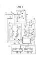
- FIG. 1 An analogue to digital converter of the counter type having characteristics high in accuracy has been frequenctly employed in audio systems such as a PCM audio system.
- FIG. 1 is a typical example of such a counter type analogue to digital converter.
- reference numeral 1 designates an integrator which is composed of an operational amplifier 1A and a capacitor 1B.
- An input terminal 3 is coupled through a sampling switch 2 to the input terminal of the integrator 1 together with a constant current source section 4.
- the sampling switch 2 is subjected to an ON-OFF control operation in response to a predetermined sampling pulse P thereby to switch an input analogue signal applied to the input terminal 3.
- the integrator 1 is operative to carry out an integrating operation for the input analogue signal applied through the sampling switch 2.
- both a constant current I from a first constant current source 4A and a constant current I 1 from a second constant current source 4B are supplied to the integrator 1 through current switches 4C and 4D, respectively, to be integrated therein.
- the constant current sources 4A and 4B and the current switches 4C and 4D constitute the constant current source section 4.
- the output terminal of the integrator 1 is coupled to the input terminal of a comparing section 5.
- the comparing section 5 is composed of a first comparator 5A, a second comparator 5B and a reference voltage source 5C.
- the output voltage of the integrator 1 is supplied to both ocmparison input terminals of the first and second comparator 5A and 5B, respectively.
- the reference voltage of the reference voltage source 5C is supplied to a reference input terminal of the first comparator 5A whereas a reference input terminal of the second comparator 5B is grounded.
- the output terminals of the first and second comparators 5A and 5B are connected to both a control section 6 and a counter section 7.
- the control section 6 is operative to produce the above-described sampling pulse P s to be supplied to a control terminal of the sampling switch 2. Further, the control section 6 is operative to produce a control signal P1 to be supplied to control terminals of the first and second comparator 5A and 5B and to produce control signals P 2 and P 3 to be supplied to control terminals of the current switches 4C and 4D, respectively.
- a comparison output C1 of the first comparator 5A and a comparison output C 2 of the second comparator 5B are supplied to the control section 6.
- the counter section 7 includes a first counter 7A for higher bits and a second counter 7B for lower bits.
- a control signal C 0 is supplied from the control section 6 to a start terminal of the first counter 7A and the comparison output C 1 of the first comparator 5A is supplied to a stop terminal of the first counter 7A and a start terminal of the second counter 7B. Further, the comparison output C 2 is supplied to a stop terminal of the second counter 7B.
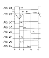
- the sampling pulse P s takes a high level as shown in Fig. 2A and this results in that the sampling switch 2 is turned on. Accordingly, the integration is carried out in.accordance with the input analogue signal in the integrator 1, so that an output voltage V 0 of the integrator 1 decreases as shown in Fig. 2B.
- This output voltage V 0 corresponds to the level of the input analog signal supplied to the input terminal 3 during the period of the time t 0 to t l .
- the sampling switch 2 When the sampling pulse P s falls down to a lower level at the time t l , the sampling switch 2 is thus turned off. At this time, the control signal P 1 from the control section 6 rises up to a high level as shown in.Fig. 2C so that both first and second comparators 5A and 5B in the comparing section 5 are turned into the active state. Simultaneously, the first counter 7A is supplied with the control signal C 0 as shown in Fig. 2F from the control section 6 thereby to commence the counting operation thereof. Further, upon falling down of the sampling pulse P s , the control signals P 2 and P 3 both having a high level as shown in Figs.
- the first counter 7A carries out the counting operation during the period of the time t 1 to t 2 . Since the control signal P 2 falls to a low level when the output voltage V 0 is equal to the reference voltage V 1 , the current switch 4C is turned off at the time t 2 , and as a result of this, the constant current I 1 is only supplied from the second constant current source 4B to the integrator 1.
- the integration is carried out in accordance with the constant current I1 in the integrator 1, and the output voltage V 0 increases linearly again during the period of the time t 2 to t 3 and is compared with the reference voltage V 2 (0V in this embodiment) in the second comparator 5B.
- the second comparator 5B At the time t 3 when the output voltage V 0 becomes equal to the reference voltage V 2 , the second comparator 5B generates the comparison output C 2 as shown in Fig. 2H.
- the comparison output C 2 rises up to a high level
- the second counter 7B is stopped. Accordingly, the second counter 7B carries out the counting operation during the period of the time t 2 to t 3 . Thereafter, when the comparison output C 2 falls down to a low level and the rising edge of the subsequent sampling pulse P appears at time t 4 , the above-described operation is performed repeatedly.
- the count result of the counter 7A at the time t 2 and the count result of the counter 7B at the time t 3 are latched and loaded to a shift register. Then, the results are derived in a serial mode, so that digital data consisting of higher bits and lower bits, which represent the integration output of the constant current (I 0 + I 1 ) and the integration output in response to the constant current I 1 , respectively, can be obtained.
- analogue to digital converter as shown in Fig. 3, in which a pair of circuit blocks containing the integrator 1 to the counter section 7 as shown in Fig. 1 and an integrator 1' to a counter section 7' similar to those shown in Fig. 1, respectively, are provided and the left and right channel signals are applied to input terminals of the circuit blocks, respectively, has been employed.
- a pair of circuit blocks containing the integrator 1 to the counter section 7 as shown in Fig. 1 and an integrator 1' to a counter section 7' similar to those shown in Fig. 1, respectively are provided and the left and right channel signals are applied to input terminals of the circuit blocks, respectively, has been employed.
- a parallel/serial converter 8 such as a shift register is further provided to the output ends of the respective counter sections 7 and 7', so that digital data obtained by subjecting the right channel audio signal to the analogue to digital conversion and that obtained by processing the left channel audio signal similarly are produced alternately as serial data.
- an analogue to digital converter of a different type in which a single analogue to digital conversion circuit arrangement is provided and, as shown in Fig. 4, an input end of an integrator 1 therein is connected to both input terminal 11 and 11' through two sampling switches 10 and 10' which are turned on alternately by a control section 9, has been proposed.
- the input terminals 11 and 11' are supplied with respectively left and right channel audio signals which are subjected alternately to an analogue to digital conversion through integrating operation and counting operation so as to produce digital data representing the both audio signals.
- the single analogue to digital conversion circuit arrangement is only required and therefore the circuit construction is made simple.
- the single analogue to digital conversion circuit arrangement is used in common with respect to two input analogue signals alternately to produce outputs converted to digital signals, there is disadvantage that a relatively long time is required to achieve analogue to digital conversion for the two input analogue signals.
- an object of the present invention is to provide an analogue to digital converter which is capable of carrying out analogue to digital conversion for two input analogue signals within a processing period substantially equal to that required for performing analogue to digital conversion for one input analogue signal with a single analogue to digital conversion circuit arrangement, and is not required to have two independent analogue to digital conversion circuit arrangements for the analogue to digital conversion for two input analogue signals.
- an analogue to digital converter comprising first and second switches for sampling first and second analogue signals alternately, first and second integrators to which the first and second analogue signals sampled by the first and second switches alternately are supplied, respectively, a constant current source section operative to supply with a constant current to the first integrator when the first switch is in the OFF state and to the second integrator when the second switch is in the OFF state, and a digital signal generating section which is supplied alternately with comparison outputs obtained by comparing output voltages of the first and second integrators derived therefrom when the constant current is supplied thereto with a predetermined voltage, respectively, and operative to generate a digital signal corresponding to a duration defined by an instant at which the constant current source section commences supplying the constant current to either the first or second integrator and an instant at which the output voltage of either the first or second integrator to which the constant current is supplied becomes equal to the predetermined voltage.
- a sampling and integrating section is independently provided for each of two input analogue signals and comparison outputs which are obtained by comparing integration outputs from both the sampling and integrating sections with a predetermined voltage, respectively, are alternately supplied to a single digital signal generating section so that analogue to digital conversion in respect of one of the two input analogue signals is carried out during each period in which sampling and integrating operation in respect of the other of the two input analogue signals is performed.
- the device it is unnecessary for the device to have two independent analogue to digital conversion circuit arrangements for two input analogue signals, and this results in that the circuit configuration of the device is simplified and analogue to digital conversion in respect of two input analogue signals can be achieved within a period substantially equal to that required for analogue to digital conversion in respect of a single input analogue signal.
- Fig. 1 is a block diagram showing an example of a conventional counter type analogue to digital converter
- Figs. 2A to 2H are waveform diagrams used for explaining the operation of the example of Fig. 1
- Figs. 3 and 4 are block diagrams each showing an example of a conventional analogue to digital converter used for analogue to digital conversion in respect of two input analogue signals
- Fig. 5 is a block diagram showing a preferred embodiment of an analogue to digital converter according to the present invention
- Figs. 6A to 61 are waveform diagrams used for explaining the operation of the embodiment shown in Fig. 5.
- Fig. 5 shows an example of an analogue to digital converter according to the present invention.
- reference numeral 20 denotes an input terminal to which a first analogue signal is delivered.
- the input terminal 20 is connected through a switch 21 formed with a field effective transistor (hereinafter referred to merely as FET) to the input terminal of a first integrator 22.
- the output terminal of the first integrator 22 is connected to a terminal provided at the input side of a switch 23 formed with an FET.
- Reference numeral 25 denotes an input terminal to which a second analog signal is delivered.
- the input terminal 25 is connected through a switch 26 formed with an FET to the input terminal of a second integrator 27.
- the output terminal of the second integrator 27 is connected to a terminal provided at the input side of a switch 28 formed with an FET.
- a junction between the switch 21 and the input terminal of the first integrator 22 and a junction between the switch 26 and the input terminal of the second integrator 27 are respectively coupled through switches 24 and 29 formed with FETs to an current output terminal of a constant current source section 32 which is similar to the constant current source section 4 shown in Fig. 1,
- the constant current source section 32 includes first and second current sources 32A and 32B and current switches 32C and 32D. Further, an inverter 30 is provided between the control terminals of the switches 23 and 28.
- the output terminals of the switches 23 and 28 are connected in common, and the common connecting point thereof is connected to a comparing section 31 which is similar to the comparing section 5 shown in Fig. 1.
- the two output terminals of the comparing section 31, that is, the output terminal from which a comparison output C 1 from a first comparator 31A is obtained and the output terminal from which a comparison output C 2 from a second comparator 31B is obtained, are connected to the input terminals of a signal processing circuit 34.
- the signal processing circuit 34 includes a first counter for higher bits, a second counter for lower bits and latch circuits provided to each of the first and second counters. Further, the output terminal of the signal processing circuit 34 is connected to a shift register 35.
- the control terminals of the switches 21, 28 and 29 and the input terminal of the inverter 30 are connected in common and the common junction thereamong is connected to the input terminal of an inverter 33.
- the output terminal of the inverter 33 is connected to both control terminals of the switches 24 and 26.
- the output terminal of a bit-clock generating circuit 36 is connected to the input terminal of a 1/8 frequency divider 37, the output terminal of which is connected through an inverter 38 to a shift clock supply terminal of the shift register 35.
- the output terminal of the 1/8 frequency devider 37 is further connected through a 1/2 frequency divider 39 to the input terminal of the inverter 33.
- a bit clock signal BC as shown in Fig. 6A which is generated by the bit clock generating circuit 36, is subjected to 1/8 frequency division in the 1/8 frequency divider 37 so that a double-frequency word clock signal 2 WC as shown in Fig. 6B is obtained.
- the signal 2 ⁇ WC is then subjected to 1/2 frequency division in the 1/2 frequency divider 39 so as to produce a word clock signal WC as shown in Fig. 6C.
- the signal WC is inverted by the inverter 33 and, as a result of this, a word clock signal WC as shown in Fig. 6D is obtained.
- the word clock signal WC takes a low level and the word clock signal WC takes a high level during a period of time T 0 to T 2 . Accordingly, the switches 26, 24 and 23 are rendered nonconductive whereas the switches 21, 29 and 28 are rendered conductive.
- the second analogue signal delivered to the input terminal 25 is supplied to the input terminal of the second integrator 27 through the switch 26. In the second integrator 27, integration in accordance with the second analogue signal is carried out, and an output voltage V L of the second integrator 27 decreases gradually as shown in Fig. 6E. This output voltage V L corresponds to the level of the second analogue signal delivered to the input terminal 25 during the period of the time T 0 to T 2 .
- the first analogue signal delivered to the input terminal 20 has been supplied through the switch 21 rendered conductive to the first integrator 22 before the time T 0 and integration in accordance therewith has been carried out in the first integrator 22 so as to produce an output voltage V R thereof.
- the output voltage V R is then supplied through the switch 23 to the input terminal of the comparing section 31.
- both the switches 32C and 32D are simultaneously turned on at the time T 0 and a sum of constant currents i 0 and i 1 supplied from the constant current sources 32A and 32B, respectively, is allowed to flow into the first integrator 22.
- the output voltage V R of the first integrator 22 increases linearly as shown in Fig. 6F.
- a control signal C c falls sown to a low level and the first counter contained in the signal processing circuit 34 is caused to start counting.
- the comparing section 31 is in the operative state.
- the level of the output voltage V R is compared with the reference voltage v 1 from the reference voltage source 31C at the first comparator 31A.
- the comparison output C 1 is supplied to the signal processing circuit 34, so that the first counter which has been caused to start counting in response to the falling edge of the control signal C c shown in Fig. 6G, is stopped counting and the second counter is caused to start counting. Simultaneously, the control signal P 2 falls down to the low level thereby to turn the current switch 32C off. As a result, the constant current i o from the constant current source 32A is interrupted to be supplied to the first integrator 22 and the constant current i 1 from the second constant current source 32B is only supplied to the integrator 22.
- the output voltage V R Due to the supply of the constant current i 1 from the second constant current source 32B, the output voltage V R further increases linearly.
- the output voltage V R is compared with the reference voltage v 2 (0V) in the comparing section 31 at the second comparator 31B.
- the comparison output C 2 is supplied from the second comparator 31B to the signal processing circuit 34 thereby to cause the second counter contained therein to stop counting.
- the contents of the first and second counters are latched by the latch circuit in the signal processing circuit 34 upon an the rising edge of the control signal C c and the first counter is reset and then caused to start counting upon the falling edge of the control signal C c .
- the word clock signals WC and WC are put in the reversed state with respect to that during the period of the time T 0 to T 2 . Accordingly, the switches 26, 24 and 23 are turned off, while the switches 21, 29 and 28 are turned on. Consequently, the output voltage V L obtained as a result of the integration carried out in the second integrator 27 during the period of the time T 0 to T 2 is supplied through the switch 28 to the input terminal of the comparing section 31.
- the supply of the constant current from the constant current source section 32 to the second integrator 27 is initiated in response to the control signals P 2 and P 3 at the time T 2 . Then, the counting and latching operations of the first and second counters in respect of the second analogue signal are carried out in the signal processing circuit 34.
- Data D R obtained from both the first and second counters and representative of the first analogue signal in the period of time T 0 to T 2' which have been latched in the signal processing circuit 34 before the time T 2' are loaded to the shift register 35 during the period of the time T 2 to T 3 within a period of time T 2 to T 4 , in which the double-frequency word clock signal 2 - WC takes the high level. Further, during a period of the time T 3 to T 4 in which the signal 2 ⁇ WC takes the low level, the data thus stored in the shift register 35 are then derived in serial mode to produce a digital conversion output DATA R in respect of the first analogue signal as shown in Fig. 6I.
- the sampling operation in respect of the second analogue signal is performed and further higher bit data and lower bit data in respect of the first analogue signal are obtained to be latched.
- the sampling operation in respect of the first analogue signal is performed, and further higher bit data and lower bit data in respect of the second analogue signal are obtained to be latched.
- the digital conversion output which is composed of the higher bit data and the lower bit data representing the second analogue signal is obtained during the period in which the word clock signal WC takes the lower level.
- the digital conversion output which is composed of the higher bit data and the lower bit data representing the first analogue signal is obtained during the period in which the word clock signal WC takes the lower level.
- the output voltages from the first and second integrators are alternatetly subjected to comparison with a predetermined certain voltage and the resultant comparison outputs are supplied to the common comparing section whose comparison output is supplied to the signal processing circuit including the counters and the latch circuits, it is possible to have such modifications that two comparing sections are respectively provided to the output sides of the first and second integrators to compare the outputs of the integrators with predetermined voltage values independently, and the comparison results from the two comparing sections are alternately supplied to the signal processing circuit including the counters and the latch circuits.
- timing at which the latched data of first and second counters are loaded to the shift register and then derived therefrom, and the duration of the above data processing may be selectively determined according to requirements within a half period of the word clock signal.
- sampling and integrating sections are independently provided in respect of respective two input analogue signals, and futher signal outputs representative of integration outputs from the sampling and integrating sections are alternately supplied to a common digital conversion output supplying section so that sampling and integrating operation in respect of one of input analogue signal is carried out during each period in which analogue to digital conversion in respect of the other of the input analogue signal is performed.
- An analogue to digital converter according to the present invention is advantageous in that analogue to digital conversion in respect of two input analogue signals is carried out accurately and therefore is suitable, for example, to be used to form an analogue to digital conversion section for recording PCM audio signals in PCM audio disk systems or PCM audio tape systems, in which analogue audio signals of left and right channels are respectively converted to PCM digital audio signals to be recorded onto either a disk medium or a magnetic tape medium.
Abstract
Description
- This invention relates to an analogue to digital converter for use in a PCM audio system and the like using a digital audio signal which is obtained by a pulse code modulation (PCM) technique.
- An analogue to digital converter of the counter type having characteristics high in accuracy has been frequenctly employed in audio systems such as a PCM audio system. Shown in Fig. 1 is a typical example of such a counter type analogue to digital converter. In Fig. 1,
reference numeral 1 designates an integrator which is composed of anoperational amplifier 1A and acapacitor 1B. Aninput terminal 3 is coupled through asampling switch 2 to the input terminal of theintegrator 1 together with a constantcurrent source section 4. Thesampling switch 2 is subjected to an ON-OFF control operation in response to a predetermined sampling pulse P thereby to switch an input analogue signal applied to theinput terminal 3. Theintegrator 1 is operative to carry out an integrating operation for the input analogue signal applied through thesampling switch 2. Further, both a constant current I from a first constantcurrent source 4A and a constant current I1 from a second constantcurrent source 4B are supplied to theintegrator 1 throughcurrent switches 4C and 4D, respectively, to be integrated therein. The constantcurrent sources current switches 4C and 4D constitute the constantcurrent source section 4. The constant currents I0 and I1 are determined to satisfy the relation of (I0 + I1) /I 1 = 27 and I0 = 127 · I1. The output terminal of theintegrator 1 is coupled to the input terminal of acomparing section 5. - The comparing
section 5 is composed of afirst comparator 5A, asecond comparator 5B and areference voltage source 5C. The output voltage of theintegrator 1 is supplied to both ocmparison input terminals of the first andsecond comparator reference voltage source 5C is supplied to a reference input terminal of thefirst comparator 5A whereas a reference input terminal of thesecond comparator 5B is grounded. The output terminals of the first andsecond comparators control section 6 and acounter section 7. - The
control section 6 is operative to produce the above-described sampling pulse Ps to be supplied to a control terminal of thesampling switch 2. Further, thecontrol section 6 is operative to produce a control signal P1 to be supplied to control terminals of the first andsecond comparator current switches 4C and 4D, respectively. A comparison output C1 of thefirst comparator 5A and a comparison output C2 of thesecond comparator 5B are supplied to thecontrol section 6. - The
counter section 7 includes afirst counter 7A for higher bits and asecond counter 7B for lower bits. A control signal C0 is supplied from thecontrol section 6 to a start terminal of thefirst counter 7A and the comparison output C1 of thefirst comparator 5A is supplied to a stop terminal of thefirst counter 7A and a start terminal of thesecond counter 7B. Further, the comparison output C2 is supplied to a stop terminal of thesecond counter 7B. - The operation of the analogue to digital converter described above will be explained hereinafter with reference to the accompanying Fig. 2.
- Now, when the input analogue signal is applied to the
input terminal 3, during a period of time t0 to t1 shown in Figs. 2A to 2H, the sampling pulse Ps takes a high level as shown in Fig. 2A and this results in that thesampling switch 2 is turned on. Accordingly, the integration is carried out in.accordance with the input analogue signal in theintegrator 1, so that an output voltage V0 of theintegrator 1 decreases as shown in Fig. 2B. This output voltage V0 corresponds to the level of the input analog signal supplied to theinput terminal 3 during the period of the time t0 to tl. When the sampling pulse Ps falls down to a lower level at the time tl, thesampling switch 2 is thus turned off. At this time, the control signal P1 from thecontrol section 6 rises up to a high level as shown in.Fig. 2C so that both first andsecond comparators section 5 are turned into the active state. Simultaneously, thefirst counter 7A is supplied with the control signal C0 as shown in Fig. 2F from thecontrol section 6 thereby to commence the counting operation thereof. Further, upon falling down of the sampling pulse Ps, the control signals P2 and P3 both having a high level as shown in Figs. 2D and 2E are supplied from thecontrol section 6 to thecurrent switches 4C and 4D so as to render thecurrent switches 4C and 4D conductive. Consequently, the sum of the constant currents I0 and I1 is allowed to flow into theintegrator 1 through theswitches 4C and 4D and theintegrator 1 carries out the integration in accordance therewith. This results in that the output voltage V0 of theintegrator 1 increases linearly. The output voltage V0 is compared with the reference voltage V1 supplied from thereference voltage source 5C in thefirst comparator 5A. Then, at the time t2 when the output voltage V0 exceeds the reference voltage V1, thefirst comparator 5A operates to produce the comparison output C1 as shown in Fig. 2G and thefirst counter 7A is stopped in response to the rising edge of the comparison output C1 whereas thesecond counter 7B is caused to commence the counting operation thereof. Accordingly, thefirst counter 7A carries out the counting operation during the period of the time t1 to t2. Since the control signal P2 falls to a low level when the output voltage V0 is equal to the reference voltage V1, thecurrent switch 4C is turned off at the time t2, and as a result of this, the constant current I1 is only supplied from the second constantcurrent source 4B to theintegrator 1. Then, the integration is carried out in accordance with the constant current I1 in theintegrator 1, and the output voltage V0 increases linearly again during the period of the time t2 to t3 and is compared with the reference voltage V2 (0V in this embodiment) in thesecond comparator 5B. At the time t3 when the output voltage V0 becomes equal to the reference voltage V2, thesecond comparator 5B generates the comparison output C2 as shown in Fig. 2H. When the comparison output C2 rises up to a high level, thesecond counter 7B is stopped. Accordingly, thesecond counter 7B carries out the counting operation during the period of the time t2 to t3. Thereafter, when the comparison output C2 falls down to a low level and the rising edge of the subsequent sampling pulse P appears at time t4, the above-described operation is performed repeatedly. - The count result of the
counter 7A at the time t2 and the count result of thecounter 7B at the time t3 are latched and loaded to a shift register. Then, the results are derived in a serial mode, so that digital data consisting of higher bits and lower bits, which represent the integration output of the constant current (I0 + I1) and the integration output in response to the constant current I1, respectively, can be obtained. - In case that, with such a conventional counter type analogue to digital converter described above, analogue to digital conversions with respect to a plurality of input analogue signals, for instance, a left-channel audio signal and a right channel audio signal contained in a stereophonic audio signal, are achieved, an analogue to digital converter as shown in Fig. 3, in which a pair of circuit blocks containing the
integrator 1 to thecounter section 7 as shown in Fig. 1 and an integrator 1' to a counter section 7' similar to those shown in Fig. 1, respectively, are provided and the left and right channel signals are applied to input terminals of the circuit blocks, respectively, has been employed. In the device of Fig. 3, a parallel/serial converter 8 such as a shift register is further provided to the output ends of therespective counter sections 7 and 7', so that digital data obtained by subjecting the right channel audio signal to the analogue to digital conversion and that obtained by processing the left channel audio signal similarly are produced alternately as serial data. - However, such a conventional device is required to have a couple of analogue to digital conversion circuit arrangements which are identical in circuit construction, and this results in the disadvantages that the device is intricate in circuit construction and the manufacturing cost thereof is increased.
- In order to eliminate the drawbacks accomanying the above-described conventional device, an analogue to digital converter of a different type in which a single analogue to digital conversion circuit arrangement is provided and, as shown in Fig. 4, an input end of an
integrator 1 therein is connected to bothinput terminal 11 and 11' through twosampling switches 10 and 10' which are turned on alternately by acontrol section 9, has been proposed. In such a device, theinput terminals 11 and 11' are supplied with respectively left and right channel audio signals which are subjected alternately to an analogue to digital conversion through integrating operation and counting operation so as to produce digital data representing the both audio signals. - In this conventional device, excepting the sampling switches, the single analogue to digital conversion circuit arrangement is only required and therefore the circuit construction is made simple. However, since the single analogue to digital conversion circuit arrangement is used in common with respect to two input analogue signals alternately to produce outputs converted to digital signals, there is disadvantage that a relatively long time is required to achieve analogue to digital conversion for the two input analogue signals.
- In view of the above, an object of the present invention is to provide an analogue to digital converter which is capable of carrying out analogue to digital conversion for two input analogue signals within a processing period substantially equal to that required for performing analogue to digital conversion for one input analogue signal with a single analogue to digital conversion circuit arrangement, and is not required to have two independent analogue to digital conversion circuit arrangements for the analogue to digital conversion for two input analogue signals.
- According to an aspect of the present invention, there is provided an analogue to digital converter comprising first and second switches for sampling first and second analogue signals alternately, first and second integrators to which the first and second analogue signals sampled by the first and second switches alternately are supplied, respectively, a constant current source section operative to supply with a constant current to the first integrator when the first switch is in the OFF state and to the second integrator when the second switch is in the OFF state, and a digital signal generating section which is supplied alternately with comparison outputs obtained by comparing output voltages of the first and second integrators derived therefrom when the constant current is supplied thereto with a predetermined voltage, respectively, and operative to generate a digital signal corresponding to a duration defined by an instant at which the constant current source section commences supplying the constant current to either the first or second integrator and an instant at which the output voltage of either the first or second integrator to which the constant current is supplied becomes equal to the predetermined voltage.
- In the analogue to digital converter thus constituted in accordance with the present invention, a sampling and integrating section is independently provided for each of two input analogue signals and comparison outputs which are obtained by comparing integration outputs from both the sampling and integrating sections with a predetermined voltage, respectively, are alternately supplied to a single digital signal generating section so that analogue to digital conversion in respect of one of the two input analogue signals is carried out during each period in which sampling and integrating operation in respect of the other of the two input analogue signals is performed. Accordingly, it is unnecessary for the device to have two independent analogue to digital conversion circuit arrangements for two input analogue signals, and this results in that the circuit configuration of the device is simplified and analogue to digital conversion in respect of two input analogue signals can be achieved within a period substantially equal to that required for analogue to digital conversion in respect of a single input analogue signal.
- In the accompanying drawings, Fig. 1 is a block diagram showing an example of a conventional counter type analogue to digital converter; Figs. 2A to 2H are waveform diagrams used for explaining the operation of the example of Fig. 1; Figs. 3 and 4 are block diagrams each showing an example of a conventional analogue to digital converter used for analogue to digital conversion in respect of two input analogue signals; Fig. 5 is a block diagram showing a preferred embodiment of an analogue to digital converter according to the present invention; and Figs. 6A to 61 are waveform diagrams used for explaining the operation of the embodiment shown in Fig. 5.
- A preferred embodiment of the present invention will be described with reference to Figs. 5 and 6 hereinafter.
- Fig. 5 shows an example of an analogue to digital converter according to the present invention.
- Initially, the circuit construction thereof will be described. In Fig. 5,
reference numeral 20 denotes an input terminal to which a first analogue signal is delivered. Theinput terminal 20 is connected through aswitch 21 formed with a field effective transistor (hereinafter referred to merely as FET) to the input terminal of afirst integrator 22. The output terminal of thefirst integrator 22 is connected to a terminal provided at the input side of aswitch 23 formed with an FET.Reference numeral 25 denotes an input terminal to which a second analog signal is delivered. Theinput terminal 25 is connected through aswitch 26 formed with an FET to the input terminal of asecond integrator 27. The output terminal of thesecond integrator 27 is connected to a terminal provided at the input side of aswitch 28 formed with an FET. A junction between theswitch 21 and the input terminal of thefirst integrator 22 and a junction between theswitch 26 and the input terminal of thesecond integrator 27 are respectively coupled throughswitches current source section 32 which is similar to the constantcurrent source section 4 shown in Fig. 1, The constantcurrent source section 32 includes first and secondcurrent sources current switches inverter 30 is provided between the control terminals of theswitches - The output terminals of the
switches section 31 which is similar to the comparingsection 5 shown in Fig. 1. The two output terminals of the comparingsection 31, that is, the output terminal from which a comparison output C1 from afirst comparator 31A is obtained and the output terminal from which a comparison output C2 from asecond comparator 31B is obtained, are connected to the input terminals of asignal processing circuit 34. Thesignal processing circuit 34 includes a first counter for higher bits, a second counter for lower bits and latch circuits provided to each of the first and second counters. Further, the output terminal of thesignal processing circuit 34 is connected to ashift register 35. - The control terminals of the
switches inverter 30 are connected in common and the common junction thereamong is connected to the input terminal of aninverter 33. The output terminal of theinverter 33 is connected to both control terminals of theswitches - The output terminal of a bit-
clock generating circuit 36 is connected to the input terminal of a 1/8frequency divider 37, the output terminal of which is connected through aninverter 38 to a shift clock supply terminal of theshift register 35. The output terminal of the 1/8frequency devider 37 is further connected through a 1/2frequency divider 39 to the input terminal of theinverter 33. - The operation of the analogue to digital converter constructed in such a manner as described above will be described with reference to the waveform diagrams of Figs. 6A to 6I.
- A bit clock signal BC as shown in Fig. 6A, which is generated by the bit
clock generating circuit 36, is subjected to 1/8 frequency division in the 1/8frequency divider 37 so that a double-frequencyword clock signal 2 WC as shown in Fig. 6B is obtained. Thesignal 2 · WC is then subjected to 1/2 frequency division in the 1/2frequency divider 39 so as to produce a word clock signal WC as shown in Fig. 6C. Thereafter, the signal WC is inverted by theinverter 33 and, as a result of this, a word clock signalWC as shown in Fig. 6D is obtained. - When the first analogue signal is delivered to the
input terminal 20 and the second analogue signal is delivered to theinput terminal 25, the word clock signal WC takes a low level and the word clock signal WC takes a high level during a period of time T0 to T2. Accordingly, theswitches switches input terminal 25 is supplied to the input terminal of thesecond integrator 27 through theswitch 26. In thesecond integrator 27, integration in accordance with the second analogue signal is carried out, and an output voltage VL of thesecond integrator 27 decreases gradually as shown in Fig. 6E. This output voltage VL corresponds to the level of the second analogue signal delivered to theinput terminal 25 during the period of the time T0 to T2. - The first analogue signal delivered to the
input terminal 20 has been supplied through theswitch 21 rendered conductive to thefirst integrator 22 before the time T0 and integration in accordance therewith has been carried out in thefirst integrator 22 so as to produce an output voltage VR thereof. The output voltage VR is then supplied through theswitch 23 to the input terminal of the comparingsection 31. Simultaneously, due to the application of such control signals P2 and P3 as used in the case described above with reference to Fig. 1 and Figs. 2A to 2H, both theswitches current sources first integrator 22. As a result, the output voltage VR of thefirst integrator 22 increases linearly as shown in Fig. 6F. At the time T0, a control signal C c falls sown to a low level and the first counter contained in thesignal processing circuit 34 is caused to start counting. At this time, since such a control signal P1 as used in the case described with reference to Fig., 1 and Figs. 2A to 2H is supplied to the comparingsection 31 with the high level, the comparingsection 31 is in the operative state. The level of the output voltage VR is compared with the reference voltage v1 from thereference voltage source 31C at thefirst comparator 31A. When the levels of both voltages compared in thefirst comparator 31C coincide with each other, the comparison output C1 is supplied to thesignal processing circuit 34, so that the first counter which has been caused to start counting in response to the falling edge of the control signal Cc shown in Fig. 6G, is stopped counting and the second counter is caused to start counting. Simultaneously, the control signal P2 falls down to the low level thereby to turn thecurrent switch 32C off. As a result, the constant current io from the constantcurrent source 32A is interrupted to be supplied to thefirst integrator 22 and the constant current i1 from the second constantcurrent source 32B is only supplied to theintegrator 22. Due to the supply of the constant current i1 from the second constantcurrent source 32B, the output voltage VR further increases linearly. The output voltage VR is compared with the reference voltage v2(0V) in the comparingsection 31 at thesecond comparator 31B. When the output voltage VR and the reference voltage v2 coincide with each other, the comparison output C2 is supplied from thesecond comparator 31B to thesignal processing circuit 34 thereby to cause the second counter contained therein to stop counting. It should be noted that the contents of the first and second counters are latched by the latch circuit in thesignal processing circuit 34 upon an the rising edge of the control signal Cc and the first counter is reset and then caused to start counting upon the falling edge of the control signal Cc. - Data DL obtained from both the first and second counters and representative of the second analogue signal, which have been latched in the
signal porocessing circuit 34 before the time T0, are loaded to theshift register 35 during the period of the time T0 to T1 within a period of the time T0 to T21 in which the double-frequencyword clock signal 2 · WC takes a high level as shown in Fig. 6H. Further, during a period of the time T1 to T2 in which thesignal 2 · WC takes a low level, the data thus stored in theshift register 35 are then derived in serial mode to produce a digital conversion output DATA L in respect of the second analogue signal as shown in Fig. 6I. - Then, during a period of the time T2 to T4, the word clock signals WC and
WC are put in the reversed state with respect to that during the period of the time T0 to T2. Accordingly, theswitches switches second integrator 27 during the period of the time T0 to T2 is supplied through theswitch 28 to the input terminal of the comparingsection 31. Simultaneously, as is similar to the case during the period of the time T0 to T2 described above, the supply of the constant current from the constantcurrent source section 32 to thesecond integrator 27 is initiated in response to the control signals P2 and P3 at the time T2. Then, the counting and latching operations of the first and second counters in respect of the second analogue signal are carried out in thesignal processing circuit 34. - Data DR obtained from both the first and second counters and representative of the first analogue signal in the period of time T0 to T2' which have been latched in the
signal processing circuit 34 before the time T2' are loaded to theshift register 35 during the period of the time T2 to T3 within a period of time T2 to T4, in which the double-frequency word clock signal 2 - WC takes the high level. Further, during a period of the time T3 to T4 in which thesignal 2 · WC takes the low level, the data thus stored in theshift register 35 are then derived in serial mode to produce a digital conversion output DATA R in respect of the first analogue signal as shown in Fig. 6I. - After the time T4, the above-described operation during the period of the time T0 to T4 is repeatedly carried out.
- In summary, during the period in which the word clock signal WC takes the lower level, the sampling operation in respect of the second analogue signal is performed and further higher bit data and lower bit data in respect of the first analogue signal are obtained to be latched. On the other hand, during the period in which the word clock signal WC takes the higher level, the sampling operation in respect of the first analogue signal is performed, and further higher bit data and lower bit data in respect of the second analogue signal are obtained to be latched. As a result, the digital conversion output which is composed of the higher bit data and the lower bit data representing the second analogue signal is obtained during the period in which the word clock signal WC takes the lower level. In contrast, during the period in which the word clock signal WC takes the higher level, the digital conversion output which is composed of the higher bit data and the lower bit data representing the first analogue signal is obtained.
- In the above described embodiment, although the output voltages from the first and second integrators are alternatetly subjected to comparison with a predetermined certain voltage and the resultant comparison outputs are supplied to the common comparing section whose comparison output is supplied to the signal processing circuit including the counters and the latch circuits, it is possible to have such modifications that two comparing sections are respectively provided to the output sides of the first and second integrators to compare the outputs of the integrators with predetermined voltage values independently, and the comparison results from the two comparing sections are alternately supplied to the signal processing circuit including the counters and the latch circuits.
- Furthermore, the timing at which the latched data of first and second counters are loaded to the shift register and then derived therefrom, and the duration of the above data processing may be selectively determined according to requirements within a half period of the word clock signal.
- As described above, in an analogue to digital converter according to the present invention, sampling and integrating sections are independently provided in respect of respective two input analogue signals, and futher signal outputs representative of integration outputs from the sampling and integrating sections are alternately supplied to a common digital conversion output supplying section so that sampling and integrating operation in respect of one of input analogue signal is carried out during each period in which analogue to digital conversion in respect of the other of the input analogue signal is performed.
- An analogue to digital converter according to the present invention is advantageous in that analogue to digital conversion in respect of two input analogue signals is carried out accurately and therefore is suitable, for example, to be used to form an analogue to digital conversion section for recording PCM audio signals in PCM audio disk systems or PCM audio tape systems, in which analogue audio signals of left and right channels are respectively converted to PCM digital audio signals to be recorded onto either a disk medium or a magnetic tape medium.
Claims (4)
Applications Claiming Priority (2)
| Application Number | Priority Date | Filing Date | Title |
|---|---|---|---|
| JP57047607A JPS58164318A (en) | 1982-03-25 | 1982-03-25 | Analog/digital converter |
| JP47607/82 | 1982-03-25 |
Publications (3)
| Publication Number | Publication Date |
|---|---|
| EP0108812A1 true EP0108812A1 (en) | 1984-05-23 |
| EP0108812A4 EP0108812A4 (en) | 1988-06-15 |
| EP0108812B1 EP0108812B1 (en) | 1990-06-13 |
Family
ID=12779917
Family Applications (1)
| Application Number | Title | Priority Date | Filing Date |
|---|---|---|---|
| EP83900968A Expired EP0108812B1 (en) | 1982-03-25 | 1983-03-25 | Analog/digital converter |
Country Status (9)
| Country | Link |
|---|---|
| US (1) | US4649372A (en) |
| EP (1) | EP0108812B1 (en) |
| JP (1) | JPS58164318A (en) |
| KR (1) | KR900008798B1 (en) |
| AU (1) | AU558940B2 (en) |
| DE (1) | DE3338544T1 (en) |
| GB (1) | GB2128826B (en) |
| NL (1) | NL190258C (en) |
| WO (1) | WO1983003501A1 (en) |
Cited By (8)
| Publication number | Priority date | Publication date | Assignee | Title |
|---|---|---|---|---|
| EP0206443A2 (en) * | 1985-06-20 | 1986-12-30 | Eaton-Kenway, Inc. | Decoder for digital radio-received data and method |
| AT390158B (en) * | 1984-06-29 | 1990-03-26 | Siemens Ag | SIGNALER |
| US5127486A (en) * | 1990-11-23 | 1992-07-07 | Eaton-Kenway, Inc. | System for sensing arrival of an automatic guided vehicle at a wire |
| US5175415A (en) * | 1990-11-27 | 1992-12-29 | Eaton-Kenway, Inc. | Combination drive-wheel mechanism and travel-sensor mechanism |
| US5187664A (en) * | 1990-11-27 | 1993-02-16 | Eaton-Kenway, Inc. | Proportional position-sensing system for an automatic guided vehicle |
| US5216605A (en) * | 1990-06-28 | 1993-06-01 | Eaton-Kenway, Inc. | Update marker system for navigation of an automatic guided vehicle |
| US5341130A (en) * | 1990-12-03 | 1994-08-23 | Eaton-Kenway, Inc. | Downward compatible AGV system and methods |
| US5539646A (en) * | 1993-10-26 | 1996-07-23 | Hk Systems Inc. | Method and apparatus for an AGV inertial table having an angular rate sensor and a voltage controlled oscillator |
Families Citing this family (9)
| Publication number | Priority date | Publication date | Assignee | Title |
|---|---|---|---|---|
| JPS6271335A (en) * | 1985-09-24 | 1987-04-02 | Sony Corp | Analog-digital or digital-analog converter |
| EP0320525B1 (en) * | 1987-12-15 | 1991-10-16 | Deutsche ITT Industries GmbH | Sample- and hold-stage and its application in parallel a/d converters |
| US5047665A (en) * | 1989-02-08 | 1991-09-10 | Burr-Brown Corporation | Low noise, low offset, high speed CMOS differential amplifier |
| US4940981A (en) * | 1989-02-08 | 1990-07-10 | Burr-Brown Corporation | Dual analog-to-digital converter with single successive approximation register |
| US4942399A (en) * | 1989-03-15 | 1990-07-17 | International Business Machines Corporation | Adaptive flash analog/digital converter for differential input signal |
| JPH03174818A (en) * | 1989-09-28 | 1991-07-30 | Nec Corp | Integration type a/d conversion circuit |
| US7336213B2 (en) * | 2004-12-17 | 2008-02-26 | Stmicroelectronics Pvt. Ltd. | Polarity independent precision measurement of an input voltage signal |
| JP5953225B2 (en) * | 2012-12-27 | 2016-07-20 | オリンパス株式会社 | AD conversion circuit and solid-state imaging device |
| EP3829058A1 (en) | 2019-11-26 | 2021-06-02 | ams International AG | Switched-capacitor amplifier and pipelined analog-to-digital converter comprising the same |
Family Cites Families (12)
| Publication number | Priority date | Publication date | Assignee | Title |
|---|---|---|---|---|
| US3242327A (en) * | 1961-10-27 | 1966-03-22 | Phillips Petroleum Co | Analysis and ratio computing apparatus |
| US3476924A (en) * | 1966-06-20 | 1969-11-04 | Electronic Associates | Integrator rate test system for an analog computer |
| US3749894A (en) * | 1971-03-19 | 1973-07-31 | R Avdeef | Analog to digital conversion and computation method |
| US4024533A (en) * | 1975-07-10 | 1977-05-17 | Analogic Corporation | Ratiometric analog-to-digital converter |
| JPS53137659A (en) * | 1977-05-09 | 1978-12-01 | Toshiba Corp | A/d conversion system |
| US4128885A (en) * | 1977-05-18 | 1978-12-05 | Motorola, Inc. | Digital circuitry for spark timing and exhaust gas recirculation control |
| JPS5821229B2 (en) * | 1977-07-30 | 1983-04-27 | 株式会社東芝 | computing device |
| JPS5442969A (en) * | 1977-09-09 | 1979-04-05 | Nec Corp | Analog-digital converter |
| JPS5827445B2 (en) * | 1978-07-14 | 1983-06-09 | タケダ理研工業株式会社 | Analog ↓-digital converter |
| US4404545A (en) * | 1979-02-13 | 1983-09-13 | Sharp Kabushiki Kaisha | Analog-to-digital converter of the dual slope type |
| US4342983A (en) * | 1980-08-11 | 1982-08-03 | Westinghouse Electric Corp. | Dynamically calibrated successive ranging A/D conversion system and D/A converter for use therein |
| JPS5868317A (en) * | 1981-10-19 | 1983-04-23 | Toshiba Corp | Analog to digital converter |
-
1982
- 1982-03-25 JP JP57047607A patent/JPS58164318A/en active Pending
-
1983
- 1983-03-25 EP EP83900968A patent/EP0108812B1/en not_active Expired
- 1983-03-25 DE DE19833338544 patent/DE3338544T1/en active Granted
- 1983-03-25 KR KR1019830001222A patent/KR900008798B1/en not_active IP Right Cessation
- 1983-03-25 NL NLAANVRAGE8320085,A patent/NL190258C/en not_active IP Right Cessation
- 1983-03-25 GB GB08330907A patent/GB2128826B/en not_active Expired
- 1983-03-25 US US06/556,710 patent/US4649372A/en not_active Expired - Fee Related
- 1983-03-25 WO PCT/JP1983/000090 patent/WO1983003501A1/en active IP Right Grant
- 1983-03-25 AU AU13715/83A patent/AU558940B2/en not_active Ceased
Non-Patent Citations (1)
| Title |
|---|
| See references of WO8303501A1 * |
Cited By (10)
| Publication number | Priority date | Publication date | Assignee | Title |
|---|---|---|---|---|
| AT390158B (en) * | 1984-06-29 | 1990-03-26 | Siemens Ag | SIGNALER |
| EP0206443A2 (en) * | 1985-06-20 | 1986-12-30 | Eaton-Kenway, Inc. | Decoder for digital radio-received data and method |
| EP0206443A3 (en) * | 1985-06-20 | 1987-10-14 | Eaton-Kenway, Inc. | Decoder for digital radio-received data and method |
| US5216605A (en) * | 1990-06-28 | 1993-06-01 | Eaton-Kenway, Inc. | Update marker system for navigation of an automatic guided vehicle |
| US5127486A (en) * | 1990-11-23 | 1992-07-07 | Eaton-Kenway, Inc. | System for sensing arrival of an automatic guided vehicle at a wire |
| US5175415A (en) * | 1990-11-27 | 1992-12-29 | Eaton-Kenway, Inc. | Combination drive-wheel mechanism and travel-sensor mechanism |
| US5187664A (en) * | 1990-11-27 | 1993-02-16 | Eaton-Kenway, Inc. | Proportional position-sensing system for an automatic guided vehicle |
| US5341130A (en) * | 1990-12-03 | 1994-08-23 | Eaton-Kenway, Inc. | Downward compatible AGV system and methods |
| US5539646A (en) * | 1993-10-26 | 1996-07-23 | Hk Systems Inc. | Method and apparatus for an AGV inertial table having an angular rate sensor and a voltage controlled oscillator |
| US5617320A (en) * | 1993-10-26 | 1997-04-01 | Hk Systems, Inc. | Method and apparatus for an AGV inertial table having an angular rate sensor and a voltage controlled oscillator |
Also Published As
| Publication number | Publication date |
|---|---|
| NL190258B (en) | 1993-07-16 |
| NL8320085A (en) | 1984-02-01 |
| EP0108812A4 (en) | 1988-06-15 |
| US4649372A (en) | 1987-03-10 |
| NL190258C (en) | 1993-12-16 |
| WO1983003501A1 (en) | 1983-10-13 |
| AU1371583A (en) | 1983-10-24 |
| GB2128826B (en) | 1986-01-29 |
| AU558940B2 (en) | 1987-02-12 |
| EP0108812B1 (en) | 1990-06-13 |
| DE3338544T1 (en) | 1984-03-22 |
| GB8330907D0 (en) | 1983-12-29 |
| KR900008798B1 (en) | 1990-11-29 |
| JPS58164318A (en) | 1983-09-29 |
| KR840004333A (en) | 1984-10-10 |
| GB2128826A (en) | 1984-05-02 |
| DE3338544C2 (en) | 1993-01-14 |
Similar Documents
| Publication | Publication Date | Title |
|---|---|---|
| US4649372A (en) | Analogue to digital converter | |
| US4773096A (en) | Digital switching power amplifier | |
| EP0047955A2 (en) | Wave-shaping circuit | |
| EP0063443A2 (en) | A digital waveform conditioning circuit | |
| GB2206009A (en) | Cmos digital-to-analog converter | |
| US3902078A (en) | Analog switch | |
| US4009475A (en) | Delta-sigma converter and decoder | |
| JPS6159015B2 (en) | ||
| US5633637A (en) | Digital-to-analog converter circuit | |
| US5613008A (en) | Hearing aid | |
| EP0208371A1 (en) | Digital-to-analog converter | |
| US4746900A (en) | Signal processing circuit | |
| US3535458A (en) | Analog multiplexing system using a separate comparator for each analog input | |
| US4573039A (en) | Digital to analog converter | |
| EP0156305B1 (en) | Digital/analogue converter | |
| KR890004226B1 (en) | Devices for processing colour signals | |
| US3656007A (en) | Voltage dependent phase switch | |
| EP0201982A2 (en) | A delta modulation decoder | |
| KR19980028843A (en) | Digital / Pulse Width Modulation (PWM) Signal Converters | |
| SU1056221A1 (en) | Function generator | |
| JPH0314827Y2 (en) | ||
| SU1056464A1 (en) | Multichannel switching device | |
| SU1041984A1 (en) | Voltage difference converter | |
| SU1378063A1 (en) | Codec of adaptive delta-modulator | |
| KR960008369Y1 (en) | Digital analog converter |
Legal Events
| Date | Code | Title | Description |
|---|---|---|---|
| PUAI | Public reference made under article 153(3) epc to a published international application that has entered the european phase |
Free format text: ORIGINAL CODE: 0009012 |
|
| 17P | Request for examination filed |
Effective date: 19840119 |
|
| AK | Designated contracting states |
Designated state(s): FR |
|
| EL | Fr: translation of claims filed | ||
| A4 | Supplementary search report drawn up and despatched |
Effective date: 19880615 |
|
| 17Q | First examination report despatched |
Effective date: 19890811 |
|
| GRAA | (expected) grant |
Free format text: ORIGINAL CODE: 0009210 |
|
| AK | Designated contracting states |
Kind code of ref document: B1 Designated state(s): FR |
|
| ET | Fr: translation filed | ||
| PLBE | No opposition filed within time limit |
Free format text: ORIGINAL CODE: 0009261 |
|
| STAA | Information on the status of an ep patent application or granted ep patent |
Free format text: STATUS: NO OPPOSITION FILED WITHIN TIME LIMIT |
|
| 26N | No opposition filed | ||
| PGFP | Annual fee paid to national office [announced via postgrant information from national office to epo] |
Ref country code: FR Payment date: 19930329 Year of fee payment: 11 |
|
| PG25 | Lapsed in a contracting state [announced via postgrant information from national office to epo] |
Ref country code: FR Effective date: 19941130 |
|
| REG | Reference to a national code |
Ref country code: FR Ref legal event code: ST |