EP0087368A2 - Interchangeable interface circuit structure - Google Patents
Interchangeable interface circuit structure Download PDFInfo
- Publication number
- EP0087368A2 EP0087368A2 EP83400354A EP83400354A EP0087368A2 EP 0087368 A2 EP0087368 A2 EP 0087368A2 EP 83400354 A EP83400354 A EP 83400354A EP 83400354 A EP83400354 A EP 83400354A EP 0087368 A2 EP0087368 A2 EP 0087368A2
- Authority
- EP
- European Patent Office
- Prior art keywords
- circuitry
- signal
- circuit
- data signal
- data
- Prior art date
- Legal status (The legal status is an assumption and is not a legal conclusion. Google has not performed a legal analysis and makes no representation as to the accuracy of the status listed.)
- Granted
Links
Images

Classifications
-
- G—PHYSICS
- G06—COMPUTING; CALCULATING OR COUNTING
- G06F—ELECTRIC DIGITAL DATA PROCESSING
- G06F3/00—Input arrangements for transferring data to be processed into a form capable of being handled by the computer; Output arrangements for transferring data from processing unit to output unit, e.g. interface arrangements
-
- G—PHYSICS
- G06—COMPUTING; CALCULATING OR COUNTING
- G06F—ELECTRIC DIGITAL DATA PROCESSING
- G06F11/00—Error detection; Error correction; Monitoring
- G06F11/22—Detection or location of defective computer hardware by testing during standby operation or during idle time, e.g. start-up testing
- G06F11/26—Functional testing
- G06F11/273—Tester hardware, i.e. output processing circuits
- G06F11/277—Tester hardware, i.e. output processing circuits with comparison between actual response and known fault-free response
-
- G—PHYSICS
- G06—COMPUTING; CALCULATING OR COUNTING
- G06F—ELECTRIC DIGITAL DATA PROCESSING
- G06F12/00—Accessing, addressing or allocating within memory systems or architectures
- G06F12/02—Addressing or allocation; Relocation
- G06F12/06—Addressing a physical block of locations, e.g. base addressing, module addressing, memory dedication
- G06F12/0646—Configuration or reconfiguration
- G06F12/0653—Configuration or reconfiguration with centralised address assignment
-
- G—PHYSICS
- G06—COMPUTING; CALCULATING OR COUNTING
- G06F—ELECTRIC DIGITAL DATA PROCESSING
- G06F13/00—Interconnection of, or transfer of information or other signals between, memories, input/output devices or central processing units
-
- G—PHYSICS
- G06—COMPUTING; CALCULATING OR COUNTING
- G06F—ELECTRIC DIGITAL DATA PROCESSING
- G06F13/00—Interconnection of, or transfer of information or other signals between, memories, input/output devices or central processing units
- G06F13/14—Handling requests for interconnection or transfer
- G06F13/20—Handling requests for interconnection or transfer for access to input/output bus
- G06F13/28—Handling requests for interconnection or transfer for access to input/output bus using burst mode transfer, e.g. direct memory access DMA, cycle steal
- G06F13/30—Handling requests for interconnection or transfer for access to input/output bus using burst mode transfer, e.g. direct memory access DMA, cycle steal with priority control
-
- G—PHYSICS
- G06—COMPUTING; CALCULATING OR COUNTING
- G06F—ELECTRIC DIGITAL DATA PROCESSING
- G06F13/00—Interconnection of, or transfer of information or other signals between, memories, input/output devices or central processing units
- G06F13/14—Handling requests for interconnection or transfer
- G06F13/36—Handling requests for interconnection or transfer for access to common bus or bus system
- G06F13/368—Handling requests for interconnection or transfer for access to common bus or bus system with decentralised access control
- G06F13/378—Handling requests for interconnection or transfer for access to common bus or bus system with decentralised access control using a parallel poll method
Abstract
Description
- In data handling systems and in particular in small computer systems, the concept of enlarging the capability/ and/or capacity of a basic system into a medium-sized system or even a large-scale system, by adding modular units. to the basic syster, has long been pursued. However, heretofore a system which permitted such "modular" addition and removal required that the system provide a number of hardware (circuitry) features to accommodate the addition and removal of the modules (i.e., interface circuits and peripherals). For instance, with respect to a first feature of prior art systems, each interface circuit card has resident decoding circuitry as part thereof, so that when the master system wants to communicate with a modular device, the interface circuitry can be addressed, irrespective of its physical location amongst the slot means which hold such interface circuit (cards). Such decoder circuitry has been fabricated, in the prior art, such that for each modular device, of a given type (e.g., a floppy disc device), a standard address circuitry configuration is provided, and if the standard address were to necessitate a change, jumpers or wirewrap changes are added or made to the address decoding circuitry to "change the address". Thirdly, while some prior art systems do permit a certain amount of interchangeability (because each interface circuit is addressable), such systems have normally required that the interface circuit cards be particularly placed in an ordered arrangement of slots to implement a method for determining priority amongst a group of active interface circuits.
- The circuitry which effects a serial scanning of the "ordered" slots has, in the prior art, been some form of "daisy chain" configuration and such configurations require that there be no empty or vacant slots between active interface circuit cards. This constraint is suffered by prior art circuits. In addition, as the number of possible modular peripherals, which could be added, were in fact increased, the amount of memory space used for I/O devices addresses, per se, increased. Further since the diagnostic routine instructions, in the prior art, use memory space in the main system, it follows that as the number of modular devices, which optionally could be added, were in fact increased, the amount of memory space used by diagnostic routine was increased. The increased use of memory space, described above, of course reduces the amount of memory space available for use with problem solving programs. In the prior art such memory restraints are overcome by adding memory capacity at additional costs.
- The present invention: eliminates the necessity of having address decoding circuitry on each interface circuit card; eliminates the "ordering" of interface circuit cards in particular slots, to accommodate a priority determination plan; permits vacant slots to exist between active interface circuit cards; eliminates excessive use of memory space to accommodate addresses for increased numbers of optional peripheral devices; and eliminates excessive use of memory space to accommodate additional diagnostic instructions as the number of optional peripheral devices is increased. It is to the foregoing concerns that the present invention offers a solution.
- The present invention is an interface circuit mounted on a circuit card, which interface circuit is provided with a means to enable it to be addressed irrespective of where it is located amongst the many possible locations into which interface circuit cards may be located on a chassis of a data handling system with which the presents invention is used. Such flexible addressing procedure is made possible in part because the physical locations, per se, are addressable and therefore a circuit- card need not have address decoding circuitry Lo effect its own addressability and such card may be in any physical location. Secondly, the interface circuit is provided with means to generate signals which identify the circuit mounted on the card at the physical location being addressed. Accordingly, after the first interrogation of a given location, to find out which circuit resides in said given location, the identification information is used in part to generate a configuration table in memory of a main system. The configuration table enables an identification address for a particular circuit to fetch the previously mentioned location address. This self-configuration enables any interface circuit card to be located into any of the holder means locations or slots in the chassis without causing the user to reprogram the operation to take into account that the interface circuit cards have been interchanged. In addition, the present interface circuit by way of further self-containment, includes a memory device wherein there is stored a predesigned diagnostic routine, particularly applicable to the interface circuit mounted on the card. This feature reduces the amount of memory space, in the main system, which is used for diagnostic routines. Further, the present interface circuit includes a priority signal arrangement which is employed with a logic circuit network in the data processing system, with which it is used, as well as a "last look" network on the card per se. The priority signal network along with an arbiter circuit in the data handling system, with which the card is employed, as well as the "last look" network on the card per se, provide a means that, irrespective of interchangeability, permits the interface card to enable a peripheral device with which it is associated to obtain control of a common data flow path in accordance with an assigned priority of the peripheral.
- The features and objects of the present invention. will become apparent in view of the following discussion taken in conjunction with the drawings in which:
- Figure 1 is a schematic block diagram of the basic interface circuit without a priority arrangement;
- Figure 2 is a block diagram depicting the circuitry required for determining priority among circuits of different priorities;
- Figure 3 is a schematic diagram of the networks employed to effect a programmable priority or any of a three-level priority recognition.
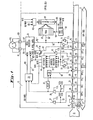
- Consider Figure 1. In Figure 1, there is shown a data address bus 11 hereinafter referred to as the D/A bus, which is a general bus that is connected to a data handling system, or a computer system, with which a present interface circuit may be employed to interface a peripheral. In the preferred embodiment there are some sixty wires or data paths located in the D/A bus 11 but obviously more or less can be used depending upon the number of circuit elements that have to be driven.
- The
data card 13, shown in Figure 1, is mounted on a chassis of the data processing system with which it is used. In Figure 1, thedata card 13 is shown mounted onto aholding means 15 which can be the base of a slot-type arrangement along which the card slides. At some given home position, the card is clamped into the slot by a rotating mechanical cam device. Actually, when the card is clamped into the slot, the circuit terminals, on the card, mesh or engage with. the counterpart circuit terminals on the holding means.. Sometimes such meshing terminals have been referred to Yaxley plugs or AMP connectors. As can be seen in Figure 1, when thecircuit card 13 is clamped into position., theconnector terminals 17 and 19 respectively engage theconnector terminals resistor 22 to ground potential. Accordingly, when the foregoing circuit is completed, there is a ground signal provided online 21 which indicates that there is a "card present" in that location. The signal online 21 is important to the data processing system, with which the circuit card is used, because the data processing system at some point would address the peripheral, with which the circuit card is associated, to either have the information transmitted therefrom or transmit information thereto. If the data processing system "believed" through some programming arrangement that a card (and therefore a peripheral), were communicatable through a given slot, but in fact, there were no interface circuit in said slot, the inquiry by the master system to that location might well result in an indication that the circuitry was not operating properly, or even worse, the failure to reply by the circuitry at the empty slot, could result in having the operation of the master system be "hung up". - Because of the way in which the logic circuitry is arranged on the circuit card, certain of the lines connected to D/A bus 11 have specific assignments. Each of the cards used with a system in which the
card 13 is employed must abide by the assignment rules so that there can be interchangeability of the cards. In the embodiment shown in Figure 1, theline 23 is connected to a line in the D/A bus 11 through which there is transmitted a read/write signal. The read/write signal online 23 is transmitted through theconnector terminals 25, through thecontrollable buffer 27 to thelogic circuitry 29. Thecontrollable buffer 27 is controlled by a control signal from the control. signal logic circuitry in the master system, which circuitry regulates the data flow into and out of thecircuit card 13. The understanding of such two way data flow can be better understood from reference to the copending U.S. patent application filed on even date and entitled, "An Arrangement To Time Separate Bidirectional Current Flow", Serial No. 351,720, and assigned to the assignee of this application. Thecontrollable buffer 27 may be any one of a number of commercially available buffers manufactured by well-known integrated circuit manufacturers and in the preferred embodiment-is an 8307 manufactured by Advanced Micro Devices Corporation. Thelogic circuitry 29 is a properly configured group of NAND gates and AND gates. The grouping of the NAND gates and the AND gates in thecircuit 29 is for the purpose of providing a read signal online 101 and a write signal online 103. Actually, the way the master system operates, there is a signal online 23 at all times indicative of a read signal unless, in fact, a write signal is generated. - In Figure 1, it can be seen that the
second line 31 is connected to the D/A bus 11 to receive a data strobe signal. The master system., with which the present interface circuit card is used, provides as part of its timing signals, first an address strobe signal during a first period of time, followed thereafter by a suitable "dead period", followed thereafter by a data strobe signal and followed thereafter by a suitable "dead period". The cycle is then repeated except if the clock signal generator is put in an "idle" condition. It is the purpose of the address strobe signal and the data strobe signal to condition the proper elements within the system, including the elements on the interface circuit card, so that during the address strobe time, the information that is being transferred, is considered address information while during the data strobe time, the information that is being transferred is considered informational data. By informational data is meant not only the kind of data that is used in= accounting problems, such as values of monies and the like, but also instructional data. The data strobe signal is transmitted along line 31., through the connector terminals 33, through the controllable buffer 35 to thelogic circuitry 29. In addition, the data strobe pulse is transmitted through thedelay line 37 to thegate circuit 39. The significance of the data strobe pulse passing through thedelay line 37, will be explained hereinafter. - The third line from the connector terminals is connected to the D/A bus 11 in order to receive a position address signal. The master system with which the
interface circuitry card 13 is employed, is formed such that each slot, or each holding member location, has a particular address. That address information is stored in the memory of the system, and when it is fetched from that memory, it goes through a decoder device, which generates a single signal. The single signal so generated is indicative of the particular slot which is being addressed. The signal online 41 is labeled PA to indicate a position address signal. The significance of the position address signal. will become apparent as the description of the identification signals is considered. The position address signal is transmitted along theline 41, through theconnector terminals 45 to thegate 39 and as well as to thedecoder 47. The PA signal enables thedecoder 47 to provide an output signal therefrom as will be discussed hereinafter. - The
fourth line 43 which is connected from the connector terminals to the D/A bus 11 is connected thereto to provide a reply signal to the master system with which the circuit card is employed. The reply signal is generated at thegate 39 in response to the simultaneous presence of a delayed data strobe pulse and a position address signal. - The reply signal is transmitted along line 48, through the
connector terminals 49, through theline 43 back to the D/A bus 11. The significance of the reply signal is explained immediately hereisafter. When the master system has addressed thecircuit card 13, or is interrogating the interface circuitry on:card 13 for data there will be present a PA signal as described before and since data. is being requested, a data strobe signal will be present. Thedelay device 37 is employed to give the system a little additional time in which to make the data that-is going to be transferred available. The master system does not want to condition the master system circuitry to receive that data, if in fact, the data is not being transferred or is not available to Be transferred. Therefore, the master system waits for the reply signal to be returned in order to continue with the program. By providing the slight delay through thedelay device 37, any circuit element which needs additional time (for instance, the data register 51 may need additional time to have the data ready for transfer) is permitted more time than would be allowed by a normal data strobe signal. - The fifth circuit which is connected from the connector terminals to the D/A bus 11 is the circuit to receive the zero through sixth bits of a set of address signals. The low order bits of a set of address signals provide certain information on the interface circuit card which information acts to address certain locations. The seven bits provide some 128 address combinations and therefore provide a circuit board with a possibility of responding to some 128 addresses. The seven bits are transmitted over the
lines 53, through theconnector terminals 55, through thebuffer 57 to theaddress register 59. It should be noted at this point that while in the drawings the data flow paths are shown as single lines, in point of fact, there may be multiple lines in parallel, such as is the case withlines 53 in order to conduct a group of parallel bits or parallel signals. The seven bits enter theaddress register 59 and as will be seen, these bits enter the address register during the address strobe period. The seven bits are held in theaddress register 59. and made available to thedecoder 47 so that when thedecoder 47 is enabled by a position address signal, thedecoder 47 will provide one of many possible output signals. - The sixth circuit path from the connector terminals is connected to the D/A bus 11 to receive the address strobe (AS) signal therealong. As explained earlier, the address strobe signal appears or is generated during a given period of time, while the data strobe signal is generated during another period of time and there is a dead period between each of these signals. The address strobe signal is transmitted along
line 61, through theconnector terminals 63, to thecontrollable buffer 65, and therefrom to the address register to enable that register during address strobe time as previously mentioned. - The seventh circuit connected from the connector terminals is connected to the D/A bus 11 to transmit an interrupt (INT) signal therealong to the master system. An interrupt signal is generated by the peripheral device, or by the interface circuitry on behalf of the peripheral device, to indicate that the peripheral device and/or the interface circuitry is experiencing an event that should be brought to the master system's attention and with which the master system must deal. For instance, by way of illustration, the data register 51 is shown having a port labelled "received data available." That port transmits information therefrom when the information has been received from the peripheral. If the peripheral, operating on its own, delivers data to the data register 51 and the data register 51 recognizes that data is available to the master system, then an interrupt signal is sent to the master system requesting the master system to find out what the condition might be with the interface circuitry. It should be noted that sometimes, if the interface circuit is a circuit that can become a master, or can act to be in control of a data flow path by way of a priority scheme, then the signal on line: 67 acts as an internal request signal. The interrupt signal is generated and transmitted along the
line 67, through theconnector terminal 69, and along theline 71 to the D/A bus 11. - The eight circuit connected from the connector terminals is connected to receive the seventh through the fifteenth bits of a set of address signals. It should be noted that the master system with which the
circuit card 13 operates, operates with words of two bytes wherein each byte has eight bits. In other words, a word in the present system has 16 bits. It will be recalled that the zero bit to the sixth bit are transmitted into the card circuitry throughlines 53 and the remaining bits, the 7th through l5th, are transmitted into the card circuitry throughlines 73. The zero through the 15th bit pass through theline 73 andline 53 through theconnector terminal 75 andconnector terminal 55 through thecontrollable buffers line 79, and thereafter seven of those bits are transmitted along theline 81, through thecontrollable buffer 83, through the interconnectingterminals 55, along thelines 53 back to the D/A bus 11. The remaining nine bits are transmitted from the juncture point 84, through the controllable buffer 85, through theconnector terminals 75, along thelines 73 to the D/A bus 11. - As also can be noted in Figure 1, there is shown a
ROM device 87. In the preferred embodiment theROM 87 is a 4K bit ROM and is employed to accomplish a number of operations. Insofar as this description goes, we will concern ourselves with the role that theROM 87 plays for two major operations. Stored in theROM 87 are the identification signals which identify thecircuit card 13 and in addition thereto, stored therein are the diagnostic routine signals which are to be used in effecting a diagnostic routine, or a testing, of the critical elements on the interface circuitry ofcard 13. - Connected to the ROM 8'/ is a ROM read
signal generator 89 whose output signal will be- referred to hereinafter as RRD. TheRRD generator 89 responds to the presnce of a data strobe (DS) signal, a read/write signal, and a W/O signal. The DS signal is transmitted online 91 after having been transmitted through the connector terminal 33. As is shown in Figure 1, theline 91 indicates that it is connected to the RRD generator 8'9. The read/write signal is transmitted online 93 after having been transmitted through theconnector terminals 25. As is shown in Figure 1, theline 93 indicates that it is connected to theRRD generator 89. Finally, the W/O signal is transmitted on line 95 from thedecoder 47. As can be seen in Figure 1, the line 95 indicates that it is connected to theRRD generator 89. The word zero or W/O signal is a signal which is generated in response to the proper combination of zero bit through sixth bit of the address information as described earlier. The proper combination of those seven bits transmitted through theaddress register 59 to thedecoder 47 generates a single signal, i.e., a W/O signal, when the system intends that theROM 87 should be read therefrom and that thecounter 97 should be incremented. The RRD signal online 99 serves to cause theROM 87 to read or to transmit signals therefrom, while the RRD signal. online 101 causes thecounter 97 to be incremented. Each time that an RRD signal is generated, thecounter 97 is incremented and causes th. next serial location in theROM 87 to be read from. It should be noted that thecounter 97 can be cleared or reset to a home position in response to an output signal from thegating circuitry 103. Theclear circuitry 103 is responsive to a data strobe signal, a read/ write signal, and a W/2 signal. The data strobe signal and the read/write signal are respectively transmitted alonglines RRD signal generator 89. The W/2 signal is generated by thedecoder 47 and is shown in Figure 1, the W/2 signal is transmitted on line 105 which in Figure 1 shows that it is connected to theclear signal generator 103. - When the diagnostic routine is to be accomplished for the interface circuitry of the
circuit card 13, th proper data storage locations of theROM 87 are read under the control ofcounter 97. The test information and instructions are transmitted along theline 107, downward along theline 79, and through thecontrollable buffers 83 and 85 to the D/A bus 11. - It should be noted that the data register 51 is connected through the connecting
terminals 109 and 111 to theperipheral connector 113. In a preferred embodiment, the information from the associated peripheral will pass through theconnector 113 and serially into the data register along theline 115, while in another operation, the information signals will be conducted serially from the data register 51 along theline 117 through theconnector terminals 109. - Because of a number of features in the present interface circuitry and its arrangement with the card, the present interface circuitry card is interchangeable into any position or slot of the chassis of the master system. As explained earlier, the closing of the
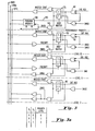
connector terminals 17 and 19 withconnector terminals card 13, enables the master system to know that, in fact, there is an option card present in that location. By having a single connector terminal, which when activated provides a signal to address a particular slot, such as the signal online 41, the interface circuit in that slot is able to respond, irrespective of what that interface circuit may represent. By having the circuitry self-contained in the sense that it can identify itself by providing identification signals fromROM 87, the interface circuit, in response to the position address signal on 41,is able to indicate to the master system what kind of an interface circuit is located in the slot being addressed. By virtue of using the identification signals in part, the address information in the master system memory can be reconfigured so that a software program which has been predesigned to call for a peripheral associated with thecircuit card 13 in accordance with certain address information, can continue to use that same address information. That address information will always operate to fetch from the master system memory the location address whereat thecard 13 is located. Finally, with respect to the basic card, the fact thatROM 87 which is present on the card has a self-contained diagnostic routine, enables the system, with which the interface circuit is used, to minimize the use of memory space for use with diagnostic routines. - Consider Figure 2. Figure 2 depicts a circuit which would be added to the basic circuit of Figure 1 in order to effect a level one priority condition, by having the circuit of Figure 2 designed to be preempted by one priority condition, but on the other hand, having the circuit designed to preempt another priority condition. The request signal demonstrated in Figure 2 is that of "direct memory access" with the shortened notation DM. "DMR" means direct memory access request, while "DMG" means direct memory access granted. It should be borne in mind that other forms of control could be requested within the spirit of the inventive concept taught here. A brief look at the table shown by Figure 3A will assist in an understanding of Figure 2. Note in Figure 3A that a circuit which is assigned a priority of PØ = O and P1 = O is considered as having a
level 0 or level zero priority. Level zero is the lowest priority in the arrangement being taught. Note further that a level "one" circuit (which is the next higher level above level zero) has priority values of P1 = 0 and P0 = 1 while a level "two" circuit (which is the highest priority circuit in the arrangement being taught) has priority values of P1 = 1 and P0 = 1. Consider Figure 2 again. - In Figure 2, there is shown a circuit having a level, one priority. The circuit is connected (along- with the circuit shown in Figure 1 and previously discussed to the peripheral device through the
connection 113A. When the peripheral device, or data responsive device, is in a state of data handling such that its circuitry needs to gain control of a common data flow path, the peripheral, or its interface circuit, generates an "internal request" signal online 121. In the present example, this is a request by the peripheral, or interface circuit, to effect a direct memory access, i.e., to transfer data directly to memory in the data processing system. The internal request signal, which is a high signal, is transmitted to the ANDgate 123. The other input signal to ANDgate 123 comes from the BPIL line. The BPlL line is shown disposed outside of the D/A bus 11 for the purposes of discussion but in the preferred embodiment, it is located in the D/A bus 11 as are the lines "BPØL" and "BUSY". - As will become clearer as this portion of the circuit is discussed, if another interface card were subjected to an internal request and it had a level two priority, then the BPlb line would be experiencing a low signal and AND
gate 123 would not be fully conditioned to provide a high output signal online 125. For the moment, let us consider that there are no higher priority circuits providing signals to the BP1L line and hence, the line is providing a high signal alongline 127, through theconnector terminals 129, through theOR gate 131 to the ANDgate 123. Accordingly, if there were no higher priority circuits requesting control of the direct memory access, then ANDgate 123 ofcircuit card 13 would provide a high signal to theNAND gate 133. TheNAND gate 133 operates such that if there are two high input signals, then there will be a low output signal and if either of the input signals is low then there will be a high output signal. The other input signal to theNAND gate 133 comes from the output terminal of the reset side of the flip-flop 135, which is high when flip-flop 135 is reset. Hence a DMR signal is. produced as the. output fromgate 133. The flip-flop 135 is a D-type flip-flop which can be transferred to its set side by a high signal online 137 only when simultaneously there is present a clock signal ,low to high transition, online 139. In the circuitry of Figure 2, the clock signal is an inverted DMG signal from the NORgate 157. In the situation under discussion, a high signal has been produced online 137 which attempts to transfer the flip-flop 135 to its set side, but since the DMG has not yet been generated, flip-flop 135 is not so transferred. Since there is one high signal to thegate 159,that gate is not conditioned to produce a master start signal. Since flip-flop 135 is in its reset state, there is a high signal online 138 to fully conditionNAND gate 133 to produce a low DMR2 signal on line 141. The signal labelled DMR2 means a request for direct memory access and from the particular card in the second slot. The DMR2 signal is transmitted through theconnector terminals 143, to the D/A bus 11. At the same time, the low signal fromthe set side of flip-flop 135 is transmitted to the NORgate 145 to provide a high impedance signal online 147, through theconnector terminals 149, to the BUSY line which indicates to the system that the circuit is not busy. The signal online 151 is the reset signal to reset flip-flop 135 and this signal is generated when the mastership is given up. The interface circuit is awaiting a DMG pulse online 153, which is transmitted through theconnector terminals 155 to the NORgate 157. The DMG signal (which is a grant signal from the master system) is a low pulse signal which provides a high pulse signal online 139, and since there is still a high signal online 137, flip-flop 135 is transferred to its set side. When the DMG pulse terminates there is a low signal togate 159 andgate 159 becomes fully conditioned to provide a master start signal. - In Figure 2, there is shown a card
control logic circuit 156, which is provided with a master start signal fromline 158, a preempt signal fromline 160, and an internal request signal fromline 121. If the master start signal is generated and the internal reguest signal continues, thecard control logic 156 provides the control signals such as DS, AS, RD/WRT and the like, which are required to effect the transfer of data to and from, between the peripheral and the system memory. When the transfer has been completed, the internal request signal will be terminated and hence, the drop master signal is generated. The drop master signal terminates the control signals from thecontrol circuit 156 and is transmitted toline 151 to reset the flip-flop 135 which in turn, terminates the master start signal .fromgate 159. It should be noted that thecard control logic 156 monitors the preempt signal even after the circuitry has taken control of the bus (i.e., has become the master). If a higher priority interface card exercises its priority, the preempt signal online 160 will condition the cardcontrol logic circuit 156 to cause it to generate a drop master signal at the end of the then current bus cycle and accordingly, reset the flip-flop 135. As described above, the drop master signal causes the circuit to give up control of the bus. - Accordingly, we have seen how the circuitry of Figure 2 will produce a DMR signal if there are no higher priority circuits seeking control. Consider now a situation where a higher priority circuit is seeking control.
- If a higher priority circuit (in this case a level "two" priority circuit) had already been subjected to an internal request prior to
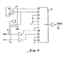
card 13 being subjected to its internal request, then the BPIL line would be low and the low signal would be transmitted through theconnector terminals 129 through theOR gate 131 to render the ANDgate 123 non-responsive to the internal request signal online 121. In short, the low signal an the BPlL line would preempt the circuit on.card 13 from generating a DMR signal on line 141. The circuitry of Figure 2 provides a. "last look" feature. If the circuit oncard 13 had already generated a DMR signal but the DMG signal had not yet been received from the data processing system and if during this time a higher priority circuit asserts or drives the BP1L line, then the "last look" feature becomes meaningful. It is apparent that the BPlL input signal to the ANDgate 123 would become low and hence, the signal online 137 would go low. Since the flip-flop 135 needs the presence of a high signal online 137 when the DMG signal is generated, it becomes apparent that there will be no master start signal and no seizing control of the bus. Hence, it is apparent that even if a circuit has completed its request and is about to receive a grant, the "last look" provides that if a higher priority circuit asserts its priority line, the request will be terminated and a subsequent grant will be ignored. - Before we examine Figure 3, examine Figure 4. In Figure 4 there are shown two
lines lines comparator device 179. Thecomparator device 179 can be any number of commercially available circuits and in a preferred embodiment is a 74S85 manufactured by Texas Instruments Corporation. As can be gleaned from Figure 4, thelines lines comparator 179 the programmed priority signals for the circuit card onlines 175 and 177 (designated AØ and Al in the comparator 179) are compared against the signals present on the BPØL and BP1L lines (designated as BØ and Bl in the comparator 179). If A is less than B, then there is provided a low preempt signal online 185. If A is greater than or the same as B, then no low preempt signal is generated. - If we now examine Figure 3, we find that in the programmable priority circuit, if there is a low signal on
line 185, the circuit is prepared by not permitting the ANDgate 161 to be fully conditioned. If the AND gate 161 -is not fully conditioned, then the NAND gate 193 will not provide a DMR signal. It should be noted in Figure 3. that thelogic circuit 186 is meant to include the circuitry of Figure 4. We find further in Figure 3 the three level circuits. In the level zero circuit, it can be seen that a low signal on the BPØL line will preempt the circuit by not permitting the ANDgate 161 to be fully conditioned. If the ANDgate 161 is not fully conditioned, then theNAND gate 163 will not provide a DMR signal. The circuitry arrangement for the flip-flop 135 is the same as that described with Figure 2. The level one circuitry is the same as that described with Figure 2. The level two circuitry differs somewhat in that there is no preemption circuit. Note that the internal request signal is transmitted directly to the flip-flop 167. Since the level two circuit is the highest priority circuit there is no higher priority to preempt it. Note also, in the level two circuit, that both the BPØL and BP1L lines are driven low to render any lower priority circuit in a preempted state. Now: if there are two circuits of the same priority requesting control of the common data flow path, then the main system circuitry provides a means to decide therebetween. - In Figure 2 note that there are shown a set of terminals A through H connected or in close proximity to the
connector terminals jumpers circuit card 13 were to operate with a level zero priority, then thejumper 134 would be located in the C-D terminals to provide a preempt signal from the BPØL line and. thejumper 132 would be removed since the level zero circuits do not drive any lines for preemption. If thecircuit card 13 were to operate with. a level two priority, then. thejumper 134 would be located in terminals G-F andjumper 132 would remain in terminal A-B which would enable the circuit to drive both the BPØL line and the BPIL line. In addition, there would need to be a jumper between terminals C-H to provide a high level signal from HV (High Voltage) to the ANDgate 123. - The jumper transitions are a simple arrangement which are shown for illustrative purposes only to effect changing the priority arrangement. The circuitry of Figure 4 is an electronic solution to the problem.
- The present system operates: (1) to permit selection from a large number of possible options without unduly using memory space for I/O addresses; (2) tomn diagnostic routines for each interface circuit without having to use excessive memory space in the memory of the main system; (3) to address interface circuit cards, irrespective of how they are interchanged in their holding means, without providing address decoding circuitry on each interface circuit card; (4) to effect a priority determination amongst requesting interface circuits having different priorities; (5) to effect a "last look" and continual monitoring after a demand for control of a common data flow path has been made, or has been granted, so that if a high priority request is made the system will act to accommodate that request; and (6) to permit interchanging the interface cards without requiring that there be no vacant slots between active interface circuit cards.
Claims (10)
Priority Applications (1)
| Application Number | Priority Date | Filing Date | Title |
|---|---|---|---|
| AT83400354T ATE57027T1 (en) | 1982-02-24 | 1983-02-21 | REPLACEABLE INTERFACE CIRCUIT STRUCTURE. |
Applications Claiming Priority (2)
| Application Number | Priority Date | Filing Date | Title |
|---|---|---|---|
| US35172182A | 1982-02-24 | 1982-02-24 | |
| US351721 | 1982-02-24 |
Publications (3)
| Publication Number | Publication Date |
|---|---|
| EP0087368A2 true EP0087368A2 (en) | 1983-08-31 |
| EP0087368A3 EP0087368A3 (en) | 1986-12-10 |
| EP0087368B1 EP0087368B1 (en) | 1990-09-26 |
Family
ID=23382088
Family Applications (1)
| Application Number | Title | Priority Date | Filing Date |
|---|---|---|---|
| EP83400354A Expired - Lifetime EP0087368B1 (en) | 1982-02-24 | 1983-02-21 | Interchangeable interface circuit structure |
Country Status (12)
| Country | Link |
|---|---|
| EP (1) | EP0087368B1 (en) |
| JP (1) | JPS5932029A (en) |
| KR (1) | KR880001416B1 (en) |
| AT (1) | ATE57027T1 (en) |
| AU (1) | AU560962B2 (en) |
| BR (1) | BR8300866A (en) |
| CA (1) | CA1189589A (en) |
| DE (1) | DE3381897D1 (en) |
| DK (1) | DK163458C (en) |
| FI (1) | FI83569C (en) |
| IE (1) | IE56342B1 (en) |
| MX (1) | MX152416A (en) |
Cited By (3)
| Publication number | Priority date | Publication date | Assignee | Title |
|---|---|---|---|---|
| EP0206321A2 (en) * | 1985-06-28 | 1986-12-30 | Bull HN Information Systems Inc. | Channel number priority assignment apparatus |
| US5038320A (en) * | 1987-03-13 | 1991-08-06 | International Business Machines Corp. | Computer system with automatic initialization of pluggable option cards |
| US5237572A (en) * | 1989-04-25 | 1993-08-17 | International Business Machines Corporation | Active remote module for the attachment of user equipments to a communication processing unit |
Families Citing this family (3)
| Publication number | Priority date | Publication date | Assignee | Title |
|---|---|---|---|---|
| CN1005658B (en) * | 1985-02-25 | 1989-11-01 | 国际标准电气公司 | Device interface controller |
| JPS62239790A (en) * | 1986-04-11 | 1987-10-20 | Matsushita Electric Ind Co Ltd | Key telephone system |
| US10544963B2 (en) | 2016-06-10 | 2020-01-28 | Fluid Handling Llc | Field configurable low water cut-offs |
Citations (4)
| Publication number | Priority date | Publication date | Assignee | Title |
|---|---|---|---|---|
| US3983540A (en) * | 1975-09-08 | 1976-09-28 | Honeywell Inc. | Rapid bus priority resolution |
| US4024505A (en) * | 1974-11-18 | 1977-05-17 | Compucorp | Interface system for coupling an indeterminate number of peripheral devices to a central processing unit |
| JPS56121153A (en) * | 1980-02-27 | 1981-09-22 | Tamura Electric Works Ltd | Self-diagnostic system of electronic apparatus |
| EP0041406A1 (en) * | 1980-06-04 | 1981-12-09 | Honeywell Inc. | Component identification in computer system |
-
1983
- 1983-02-09 MX MX196213A patent/MX152416A/en unknown
- 1983-02-17 FI FI830539A patent/FI83569C/en not_active IP Right Cessation
- 1983-02-21 EP EP83400354A patent/EP0087368B1/en not_active Expired - Lifetime
- 1983-02-21 CA CA000422035A patent/CA1189589A/en not_active Expired
- 1983-02-21 DE DE8383400354T patent/DE3381897D1/en not_active Expired - Fee Related
- 1983-02-21 AT AT83400354T patent/ATE57027T1/en not_active IP Right Cessation
- 1983-02-22 DK DK076083A patent/DK163458C/en not_active IP Right Cessation
- 1983-02-23 BR BR8300866A patent/BR8300866A/en not_active IP Right Cessation
- 1983-02-23 IE IE389/83A patent/IE56342B1/en not_active IP Right Cessation
- 1983-02-23 AU AU11784/83A patent/AU560962B2/en not_active Ceased
- 1983-02-23 KR KR8300739A patent/KR880001416B1/en not_active IP Right Cessation
- 1983-02-24 JP JP58030169A patent/JPS5932029A/en active Granted
Patent Citations (4)
| Publication number | Priority date | Publication date | Assignee | Title |
|---|---|---|---|---|
| US4024505A (en) * | 1974-11-18 | 1977-05-17 | Compucorp | Interface system for coupling an indeterminate number of peripheral devices to a central processing unit |
| US3983540A (en) * | 1975-09-08 | 1976-09-28 | Honeywell Inc. | Rapid bus priority resolution |
| JPS56121153A (en) * | 1980-02-27 | 1981-09-22 | Tamura Electric Works Ltd | Self-diagnostic system of electronic apparatus |
| EP0041406A1 (en) * | 1980-06-04 | 1981-12-09 | Honeywell Inc. | Component identification in computer system |
Non-Patent Citations (5)
| Title |
|---|
| COMPUTER DESIGN, January 1977, pages 98-101, Concord, US; S. WASER: "p/ROM card simplifies computer diagnosis" * |
| EDN MAGAZINE, vol. 26, no. 3, February 1981, page 88, Boston, Massachusetts, US; N.D. MACKINTOSH: "Interrogation tells muP which boards are present" * |
| IBM TECHNICAL DISCLOSURE BULLETIN, vol. 22, no. 10, March 1980, pages 4615,4616, New York, US; S. MEGURO: "Automatic module detection" * |
| IEEE 1981 IECI PROCEEDINGS, San Francisco, C.A., US, 9th-12th November 1981, pages 13-17; "Applications of mini and microcomputers", C.J. TAVORA et al.: "An electric nameplate prototype" * |
| PATENTS ABSTRACTS OF JAPAN, vol. 5, no. 201 (P-94)[873], 19th December 1981; & JP - A - 56 121 153 (TAMURA DENKI SEISAKUSHO K.K.) 22-09-1981 * |
Cited By (4)
| Publication number | Priority date | Publication date | Assignee | Title |
|---|---|---|---|---|
| EP0206321A2 (en) * | 1985-06-28 | 1986-12-30 | Bull HN Information Systems Inc. | Channel number priority assignment apparatus |
| EP0206321A3 (en) * | 1985-06-28 | 1988-09-07 | Honeywell Bull Inc. | Channel number priority assignment apparatus |
| US5038320A (en) * | 1987-03-13 | 1991-08-06 | International Business Machines Corp. | Computer system with automatic initialization of pluggable option cards |
| US5237572A (en) * | 1989-04-25 | 1993-08-17 | International Business Machines Corporation | Active remote module for the attachment of user equipments to a communication processing unit |
Also Published As
| Publication number | Publication date |
|---|---|
| AU1178483A (en) | 1983-09-01 |
| EP0087368B1 (en) | 1990-09-26 |
| KR840003854A (en) | 1984-10-04 |
| CA1189589A (en) | 1985-06-25 |
| FI830539L (en) | 1983-08-25 |
| AU560962B2 (en) | 1987-04-30 |
| DK76083A (en) | 1983-08-25 |
| DK163458B (en) | 1992-03-02 |
| DE3381897D1 (en) | 1990-10-31 |
| FI830539A0 (en) | 1983-02-17 |
| EP0087368A3 (en) | 1986-12-10 |
| JPS6143746B2 (en) | 1986-09-29 |
| ATE57027T1 (en) | 1990-10-15 |
| DK163458C (en) | 1992-07-20 |
| KR880001416B1 (en) | 1988-08-01 |
| IE830389L (en) | 1983-08-24 |
| BR8300866A (en) | 1983-11-16 |
| IE56342B1 (en) | 1991-07-03 |
| JPS5932029A (en) | 1984-02-21 |
| DK76083D0 (en) | 1983-02-22 |
| FI83569C (en) | 1991-07-25 |
| FI83569B (en) | 1991-04-15 |
| MX152416A (en) | 1985-07-10 |
Similar Documents
| Publication | Publication Date | Title |
|---|---|---|
| US4556953A (en) | Interchangeable interface circuitry arrangements for use with a data processing system | |
| US6393576B1 (en) | Apparatus and method for communication between integrated circuit connected to each other by a single line | |
| US5001624A (en) | Processor controlled DMA controller for transferring instruction and data from memory to coprocessor | |
| US5598542A (en) | Method and apparatus for bus arbitration in a multiple bus information handling system using time slot assignment values | |
| US4763249A (en) | Bus device for use in a computer system having a synchronous bus | |
| US4631670A (en) | Interrupt level sharing | |
| US4495571A (en) | Data processing system having synchronous bus wait/retry cycle | |
| US4670855A (en) | Interchangeable interface circuit structure | |
| US4769768A (en) | Method and apparatus for requesting service of interrupts by selected number of processors | |
| EP0506021A1 (en) | Method and apparatus for providing initial instructions in a multiple computer system | |
| US4661905A (en) | Bus-control mechanism | |
| US6216191B1 (en) | Field programmable gate array having a dedicated processor interface | |
| EP0140751A2 (en) | Cache invalidation mechanism for multiprocessor systems | |
| US5148545A (en) | Bus device which performs protocol confidential transactions | |
| US5101479A (en) | Bus device for generating and responding to slave response codes | |
| US5341480A (en) | Method and apparatus for providing a two conductor serial bus | |
| EP0301610B1 (en) | Data processing apparatus for connection to a common communication path in a data processing system | |
| US4535453A (en) | Signaling input/output processing module for a telecommunication system | |
| US5119292A (en) | Bus device which abstains from round robin arbitration | |
| KR930002787B1 (en) | Universal peripheral controller self-configuring bootloadable ramware | |
| JPS5875232A (en) | System for providing multiplex withdrawing bus cycle operation | |
| US4300194A (en) | Data processing system having multiple common buses | |
| US4340933A (en) | Data processing system having centralized nonexistent memory address detection | |
| JPH0626336B2 (en) | Control link | |
| EP0087368A2 (en) | Interchangeable interface circuit structure |
Legal Events
| Date | Code | Title | Description |
|---|---|---|---|
| PUAI | Public reference made under article 153(3) epc to a published international application that has entered the european phase |
Free format text: ORIGINAL CODE: 0009012 |
|
| AK | Designated contracting states |
Designated state(s): AT BE CH DE FR GB IT LI LU NL SE |
|
| PUAL | Search report despatched |
Free format text: ORIGINAL CODE: 0009013 |
|
| AK | Designated contracting states |
Kind code of ref document: A3 Designated state(s): AT BE CH DE FR GB IT LI LU NL SE |
|
| 17P | Request for examination filed |
Effective date: 19870603 |
|
| 17Q | First examination report despatched |
Effective date: 19880408 |
|
| GRAA | (expected) grant |
Free format text: ORIGINAL CODE: 0009210 |
|
| AK | Designated contracting states |
Kind code of ref document: B1 Designated state(s): AT BE CH DE FR GB IT LI LU NL SE |
|
| REF | Corresponds to: |
Ref document number: 57027 Country of ref document: AT Date of ref document: 19901015 Kind code of ref document: T |
|
| REF | Corresponds to: |
Ref document number: 3381897 Country of ref document: DE Date of ref document: 19901031 |
|
| ITF | It: translation for a ep patent filed |
Owner name: STUDIO TORTA SOCIETA' SEMPLICE |
|
| ET | Fr: translation filed | ||
| PLBE | No opposition filed within time limit |
Free format text: ORIGINAL CODE: 0009261 |
|
| STAA | Information on the status of an ep patent application or granted ep patent |
Free format text: STATUS: NO OPPOSITION FILED WITHIN TIME LIMIT |
|
| 26N | No opposition filed | ||
| PGFP | Annual fee paid to national office [announced via postgrant information from national office to epo] |
Ref country code: FR Payment date: 19930111 Year of fee payment: 11 Ref country code: CH Payment date: 19930111 Year of fee payment: 11 |
|
| PGFP | Annual fee paid to national office [announced via postgrant information from national office to epo] |
Ref country code: DE Payment date: 19930112 Year of fee payment: 11 |
|
| PGFP | Annual fee paid to national office [announced via postgrant information from national office to epo] |
Ref country code: SE Payment date: 19930113 Year of fee payment: 11 |
|
| PGFP | Annual fee paid to national office [announced via postgrant information from national office to epo] |
Ref country code: LU Payment date: 19930114 Year of fee payment: 11 Ref country code: AT Payment date: 19930114 Year of fee payment: 11 |
|
| PGFP | Annual fee paid to national office [announced via postgrant information from national office to epo] |
Ref country code: BE Payment date: 19930125 Year of fee payment: 11 |
|
| PGFP | Annual fee paid to national office [announced via postgrant information from national office to epo] |
Ref country code: GB Payment date: 19930129 Year of fee payment: 11 |
|
| ITTA | It: last paid annual fee | ||
| PGFP | Annual fee paid to national office [announced via postgrant information from national office to epo] |
Ref country code: NL Payment date: 19930228 Year of fee payment: 11 |
|
| EPTA | Lu: last paid annual fee | ||
| PG25 | Lapsed in a contracting state [announced via postgrant information from national office to epo] |
Ref country code: LU Free format text: LAPSE BECAUSE OF NON-PAYMENT OF DUE FEES Effective date: 19940221 Ref country code: GB Effective date: 19940221 Ref country code: AT Effective date: 19940221 |
|
| PG25 | Lapsed in a contracting state [announced via postgrant information from national office to epo] |
Ref country code: SE Effective date: 19940222 |
|
| PG25 | Lapsed in a contracting state [announced via postgrant information from national office to epo] |
Ref country code: LI Effective date: 19940228 Ref country code: CH Effective date: 19940228 Ref country code: BE Effective date: 19940228 |
|
| BERE | Be: lapsed |
Owner name: DIGITAL EQUIPMENT CORP. Effective date: 19940228 |
|
| PG25 | Lapsed in a contracting state [announced via postgrant information from national office to epo] |
Ref country code: NL Effective date: 19940901 |
|
| NLV4 | Nl: lapsed or anulled due to non-payment of the annual fee | ||
| GBPC | Gb: european patent ceased through non-payment of renewal fee |
Effective date: 19940221 |
|
| PG25 | Lapsed in a contracting state [announced via postgrant information from national office to epo] |
Ref country code: FR Effective date: 19941031 |
|
| REG | Reference to a national code |
Ref country code: CH Ref legal event code: PL |
|
| PG25 | Lapsed in a contracting state [announced via postgrant information from national office to epo] |
Ref country code: DE Effective date: 19941101 |
|
| REG | Reference to a national code |
Ref country code: FR Ref legal event code: ST |
|
| EUG | Se: european patent has lapsed |
Ref document number: 83400354.3 Effective date: 19940910 |