EP0084871A2 - Method and apparatus for reducing semiconductor laser optical noise - Google Patents
Method and apparatus for reducing semiconductor laser optical noise Download PDFInfo
- Publication number
- EP0084871A2 EP0084871A2 EP83100531A EP83100531A EP0084871A2 EP 0084871 A2 EP0084871 A2 EP 0084871A2 EP 83100531 A EP83100531 A EP 83100531A EP 83100531 A EP83100531 A EP 83100531A EP 0084871 A2 EP0084871 A2 EP 0084871A2
- Authority
- EP
- European Patent Office
- Prior art keywords
- semiconductor laser
- semi
- wave plate
- objective lens
- reducing
- Prior art date
- Legal status (The legal status is an assumption and is not a legal conclusion. Google has not performed a legal analysis and makes no representation as to the accuracy of the status listed.)
- Granted
Links
Images


Classifications
-
- G—PHYSICS
- G11—INFORMATION STORAGE
- G11B—INFORMATION STORAGE BASED ON RELATIVE MOVEMENT BETWEEN RECORD CARRIER AND TRANSDUCER
- G11B7/00—Recording or reproducing by optical means, e.g. recording using a thermal beam of optical radiation by modifying optical properties or the physical structure, reproducing using an optical beam at lower power by sensing optical properties; Record carriers therefor
- G11B7/12—Heads, e.g. forming of the optical beam spot or modulation of the optical beam
- G11B7/125—Optical beam sources therefor, e.g. laser control circuitry specially adapted for optical storage devices; Modulators, e.g. means for controlling the size or intensity of optical spots or optical traces
- G11B7/127—Lasers; Multiple laser arrays
-
- H—ELECTRICITY
- H01—ELECTRIC ELEMENTS
- H01S—DEVICES USING THE PROCESS OF LIGHT AMPLIFICATION BY STIMULATED EMISSION OF RADIATION [LASER] TO AMPLIFY OR GENERATE LIGHT; DEVICES USING STIMULATED EMISSION OF ELECTROMAGNETIC RADIATION IN WAVE RANGES OTHER THAN OPTICAL
- H01S3/00—Lasers, i.e. devices using stimulated emission of electromagnetic radiation in the infrared, visible or ultraviolet wave range
- H01S3/005—Optical devices external to the laser cavity, specially adapted for lasers, e.g. for homogenisation of the beam or for manipulating laser pulses, e.g. pulse shaping
-
- H—ELECTRICITY
- H01—ELECTRIC ELEMENTS
- H01S—DEVICES USING THE PROCESS OF LIGHT AMPLIFICATION BY STIMULATED EMISSION OF RADIATION [LASER] TO AMPLIFY OR GENERATE LIGHT; DEVICES USING STIMULATED EMISSION OF ELECTROMAGNETIC RADIATION IN WAVE RANGES OTHER THAN OPTICAL
- H01S5/00—Semiconductor lasers
- H01S5/06—Arrangements for controlling the laser output parameters, e.g. by operating on the active medium
- H01S5/065—Mode locking; Mode suppression; Mode selection ; Self pulsating
-
- H—ELECTRICITY
- H01—ELECTRIC ELEMENTS
- H01S—DEVICES USING THE PROCESS OF LIGHT AMPLIFICATION BY STIMULATED EMISSION OF RADIATION [LASER] TO AMPLIFY OR GENERATE LIGHT; DEVICES USING STIMULATED EMISSION OF ELECTROMAGNETIC RADIATION IN WAVE RANGES OTHER THAN OPTICAL
- H01S5/00—Semiconductor lasers
- H01S5/06—Arrangements for controlling the laser output parameters, e.g. by operating on the active medium
- H01S5/068—Stabilisation of laser output parameters
-
- H—ELECTRICITY
- H01—ELECTRIC ELEMENTS
- H01S—DEVICES USING THE PROCESS OF LIGHT AMPLIFICATION BY STIMULATED EMISSION OF RADIATION [LASER] TO AMPLIFY OR GENERATE LIGHT; DEVICES USING STIMULATED EMISSION OF ELECTROMAGNETIC RADIATION IN WAVE RANGES OTHER THAN OPTICAL
- H01S5/00—Semiconductor lasers
- H01S5/005—Optical components external to the laser cavity, specially adapted therefor, e.g. for homogenisation or merging of the beams or for manipulating laser pulses, e.g. pulse shaping
Definitions
- the present invention relates to a method and an apparatus for reducing an optical noise generated by a semiconductor laser in an optical information processing system such as an optical disc player which utilizes a semiconductor laser as a light source.
- a single longitudinal mode semiconductor laser which oscillates at one wave has a very small astigmatism and hence can highly converge a light spot emitted from one facet of a device at an external record medium.
- a light spot diameter X/NA on a disc surface is no larger than 1.75 ⁇ m.
- optical isolator is used to minimize a light fed back to the semiconductor laser device in order to prevent the semiconductor laser noise due to the feedback light.
- a magnitude of the optical noise significantly changes by a small change in the amount of feedback light, and when the amount of feedback light reaches a pp roxi- mately 0.1% of the amount of emitted light, the optical noise abruptly increases. Accordingly, in the past, it has been required to increase the precision of the optical parts, reduces the variation among the parts and increase the precision in an assembly work. Therefore, the prior art apparatus is not suitable for mass production.
- Fig. la shows a basic construction of an optical system of an optical disc player pickup.
- a laser beam emitted from an emitting point 8 of a semiconductor laser 1 is collimated by a coupling lens 2 and the collimated light beam passes through a polarization beamsplitter 3 and a quarter wave plate 4 and then is converged by a objective lens 5 into a light spot 9 or a reflection plane 6 on a disc.
- the light reflected by the reflection plane again passes through the objective lens 5 and the quarter wave plate 4 and deflected normally by the polarization beamsplitter 3 and then reaches a light detector 7 which converts the light to an electric signal.
- the combination of the quarter wave plate 4 and the polarization beamsplitter 3 is principally designed to prevent the feedback of the reflected light from the disc to the semiconductor laser.
- the linearly polarized light beam emitted from the semiconductor laser is applied to the quarter wave plate 4a with a polarization plane thereof being at 45 degrees to a crystal axis of the quarter wave plate so that the laser beam passed through the quarter wave plate is circularly polarized.
- this laser beam is reflected by the reflection plane and again passes through the quarter wave plate, it is linearly polarized with the polarization plane thereof being rotated by 90 degrees with respect to that of the original beam.
- the light beam having the p olariza- tion of 90 degrees does not transmit through the polarization beamsplitter but it is reflected thereby so that the light beam is not fed back to the semiconductor laser.
- the precision error of the assembly work and an optical anisotropy (birefraction). For example, assuming that a ratio of light distributed to the light detector 7 to that to the semiconductor laser 1 is 200 when the reflected light from the reflection plane 6 of the disc in Fig.
- a coupling efficiency between the semiconductor laser 1 and the coupling lens 2 that is, a ratio of a total amount of light emitted forwardly of the semiconductor laser to the amount of light passed through the coupling lens 2 is 20% and a reflection factor of the reflection plane is 90%, approximately 0.09 - 0.1% of the light emitted forwardly of the semiconductor laser is fed back to the emitting point 8.
- This feedback light causes the increase of the optical noise. It is, therefore, necessary to severely control the tolerance of the optical parts and the variation among the parts to minimize the amount of feedback light.
- 1 - 10% of the total amount of light emitted per one facet of the semiconductor laser is fed back to the emitting point of the semiconductor laser in the optical information processing apparatus which uses the single longitudinal mode semiconductor laser as the light source.
- the light output fluctuates when the light is fed back to the laser device and thus causes the optical noise. Accordingly, in the prior art, an effort has been made to prevent the feedback of the light.
- a noise level does not monotonously increase with the amount of feedback light but exhibits a peak at a certain amount of feedback light and decreases as the amount of feedback further increases.
- An example thereof is shown in Fig. 2, in which an abscissa represents a feedback light factor, that is, a rate of the amount of feedback light to the emitting point of the device to the total amount of light emitted per one facet of the single longitudinal mode semiconductor laser, and an ordinate represents a plot of maximum relative noise intensities per band width of 1 kHz with a P.C.
- a relative noise intensity of 10 -13 corresponds to an S/N ratio of 90 dB when measured in a band width of-10 kHz (10 4 Hz).
- Fig. 3a shows a change of the relative noise intensity for the 0.1% feedback factor with an abscissa representing a temperature
- Fig. 3b shows a similar change for 2% feedback factor.
- Fig. la the disc is substituted by a mirror and a ratio of light feedback is set at some levels by the rotation of the quarter wave plate 4.
- the output of the light detector 7 is supplied to an amplifier and the amplified output is passed through a band-pass filter to eliminate a noise component of 500 kHz.
- the output of the filter is supplied to an X-Y recorder.
- a light output of the single longitudinal mode semiconductor laser 1 is kept at 3 milli-watts and the laser 1 is mounted on a Peltier device a device temperature is changed from 20°C to 60°C by a Peltier controller and a change of laser temperature is measured by a thermometer, an output of which is supplied to an X-axis of the X-Y recorder to measure the noise level.
- Fig. 3a shows a change of the relative noise intensity for a 0.5% feedback.
- Fig. 3b shows a change for a 2% feedback.
- Fig. 2 shows a plot of maximum noise levels measured when the feedback factor changes.
- Fig. 2 It is seen from Fig. 2 that the peak of the noise is in the vicinity of 0.1% of the feedback light factor, and when the feedback light factor further increases, the noise reduces and the change of noise is small.
- the curve of Fig. 2 slightly changes depending on the laser device and an optical distance between the one facet of the laser and the reflection plane. When the feedback light factor is larger than 1%, it is beyond the peak of the noise in most cases and the variation of noise is small.
- the noise intensity by the light feedback of 2% is more than 10 dB lower than that of 0.1% feedback and hence it is effective to reduce the noise.
- the noise can be reduced not by reducing the feedback light factor as is done in the prior art but by increasing it to 1% or more so that the semiconductor laser is operated on the right side of the peak.
- the variation width of the optical noise is small when the feedback light factor is increased. Accordingly, by increasing the feedback light factor, less precision of the optical parts is required and substantially constant optical noise intensity is obtained even if the amount of feedback shifts due to the variation among the parts. Therefore, the present apparatus is suited to mass production.
- the feedback light factor is preferably between 1% and 10%, and more preferably between 1% and 3% from the standpoint of the S/N ratio.
- the feedback light factor is calculated based on a coupling efficiency n of the coupling lens and an efficiency of the optical parts as follows.
- the optical system is designed so that the feedback light factor is between 1% and 10%.
- the construction of the optical system remains the same as that of Fig. la and an angle 6 between a polarization plane of the laser beam applied to the quarter wave plate and a crystal axis of the quarter wave plate is rotated by 45 degrees of a standard angle as shown in Fig. 4a to attain a predetermined feedback.
- the feedback light factor F to the semiconductor laser is next calculated.
- the coupling efficiency ⁇ between the semiconductor laser 1 and the coupling lens 2 includes a loss L 2 of the coupling lens 2 in an optical path to the reflector plate 6.
- Optical losses due to surface reflection and attenuation in one way of the lenses 2 and 5, the polarization beamsplitter 3 and the quarter wave plate 4 are now represented by L 2r L 5 , L 3 and L 4 , respectively, a reflection factor at a mirror surface of the disc 6 is represented by R 6 , and the transmission factor of the reflected light from the disc into the laser 1 through the polarization beamsplitter 3 is represented by T 3 . It is assumed that no other optical loss is included.
- the emitting point 8 of the semiconductor laser and the spot 9 on the disc are in a focusing relation with each other. Therefore, it can be considered that the light applied to the coupling lens 2 from the reflected light from the disc, less the loss L 2 by the lens 2 is returned to the emitting point 8.
- T 3 is selected to 5.9% or more and the positioning angle 8 of the quarter wave is 38° or 52° from the formula (1).
- the quarter wave plate is rotated by more than ⁇ 7° from the standard positioning angle.
- T 3 is selected to 12% and the positioning angle 9 of the quarter wave plate is 35° or 55°.
- the quarter wave plate is rotated by approximately ⁇ 10° from the standard positioning angle.
- the quarter plate is rotated such that the light amount of the light detector 7 is reduced by T 3 from the maximum.
- T 3 is 58% and ⁇ is 20° or 70° but the signal light amount is also reduced by T 3 . Accordingly, when a large feedback light factor is selected, it is necessary to consider the compliance with the S/N ratio of other portion such as electric system.
- FIG. 5 A basic construction of Fig. 5 is similar to that of Fig. la except that an optical system includes a diffraction grating 10 and tracking error detecting light detectors 12a and 12b and a detecting lens 11 in order to attain a so-called three-spot tracking in the optical disc player pickup.
- a collimated laser beam emitted from the laser 1 passes through the diffraction grating 10 in which it is split into 0-order light, tl-order lights and higher order light.
- the fl-order lights produce spots 13a and 13b by the objective lens 5 on both sides of a main spot 9 with a displacement of an approximately half of the main spot track width and each at opposite positions in a longitudinal direction of the track.
- the light detectors 12a and 12b detect reflected lights from the spots 13a and 13b to produce a tracking error from a differential signal.
- a diffraction light when the light is returned to the laser 1 through the rotated quarter wave plate 4, a diffraction light produces when the light passes through the diffraction grating 10 in its return path.
- a part of the reflected light from the main spot produces spots 15a and 15b on the same plane as the laser one facet. Accordingly, when a diffraction grating is used in the optical system, the quantity of light which returns to the emitting point 8 due to diffraction is reduced. A part of the 1- and more-order diffraction lights, for example, +l-order diffraction light in its forth path is reflected by the disk and is again diffracted by the diffraction grating to return the emitting point. The light quantity which returns to the emitting point due to the 1- and more-order diffraction lights is negligible in calculation since it is generally small as compared with that due to the 0-order diffraction light. Accordingly, the feedback light factor is calculated in the following manner.
- T 3 is selected to 12.5%, and the positioning angle ⁇ of the quarter wave plate is 35° or 55°. That is, it is rotated by more than ⁇ 10° from the standard positioning angle. If F of more than 2% is desired, T is selected to 25% and 6 is 30° or 60°, that is, the quarter wave plate is rotated by approximately ⁇ 15°.
- a beam spread angle of the semiconductor laser in a thickness direction of the semiconductor laser chip is different from that in a normal direction.
- the coupling lens 2 having a small value of numerical aperture is used so that only central portion of the laser beam is utilized.
- one or two Brewster prisms 16a and 16b are used to shape the beam.
- the coupling lens 2 may have a relatively large numerical aperture such as 0.5 so that the light utilization efficiency is increased.
- Fig. 6a one Brewster prism 16a is used. It is assumed that the numerical aperture of the coupling lens 2 is 0.5 and n is 80%. It is also assumed that a loss L 16 of the prism 16a is 2% in one way and the other efficiencies of the optical system is same as those in Fig. 1.
- the feedback light factor F is given by
- T 3 When F is 1% - 10%, then T 3 is 1.5 - 15% and the quarter wave plate is rotated by ⁇ 3.5° - 11.5°. At a standard feedback light factor of 2%, T 3 is 3% and ⁇ is 40° or 50° and the quarter wave plate is rotated by approximately ⁇ 5°.
- Fig. 6b which uses two Brewster prisms
- the feedback light factor F of 1 - 10% is attained by T 3 of 1.6 - 16%.
- the rotation angle of the quarter wave plate is substantially same as that when one Brewster prism is used, that is, ⁇ 3.5° - ⁇ 12° at the standard feedback light factor of 2%, T 3 is 3.2% and the rotation angle of the quarter wave plate is ⁇ 5°.
- the transmission factor T 3 of the polarization beamsplitter is determined by taking the 0-order light transmission factor T G 2 in both ways into consideration.
- the objective lens 5 facing the disc is fixed and the light loss in one way is 1%.
- a diameter of the objective lens 5 is reduced relative to a diameter of the coupling lens 2 to allow the parallel movement. Accordingly, it is necessary to fully consider a light intensity reduction by a areal reduction.
- the output light intensity is approximately 0.6 times of the input light intensity. This should be taken into consideration of the above formula.
- An optical element having a phase shift preset to attain the desired T 3 may be used in place of the quarter wave plate.
- the transmission factor T 3 of the polarization beamsplitter is set by the quarter wave plate such that the feedback light factor to the emitting point is 1 - 10% in order to reduce the laser noise.
- the signal light intensity is obtained with a relatively small laser output.
- the quarter wave plate 4 and the polarization beamsplitter 3 of Fig. 1 are substituted by a prism 17 which is hardly subjected to an influence of the polarization and has specific transmission factor and reflection factor.
- a prism 17 which is hardly subjected to an influence of the polarization and has specific transmission factor and reflection factor.
- Such an optical element is hereinafter referred to as a semi-transmissive prism.
- a desired feedback light factor is attained in the following manner.
- T 17 represents a transmission factor of the semi-transmissive prism to an incident light
- R17 represents a reflection factor.
- a sum of T 17 and R 17 is not necessarily unity because of absorption by the semi-transmissive prism.
- the light emitted from the semiconductor laser I is collimated by the coupling lens 2 and then applied to the semi-transmissive prism 17. Only the T 17 portion of the incident light transmits to the reflection plane and the R 17 portion is deflected oppositely to the light detector 7. As the light reflected by the reflection plane 6 reenters the semi-transmissive prism 17, it is split into the transmission light and the reflection light and the light corresponding to_R 17 reaches the light detector 7 while the light corresponding to T 17 is fed back to the emitting point 8.
- the transmission factor T 17 of the semi-transmissive prism is selected to 22 - 77%.
- T 3 is 34%. This is attained by setting the reflection factor R 17 of the semi-transmissive prism to 66% and the transmission factor T 17 to 34%.
- Fi g. 8 shows an embodiment which uses a semi-transmissive prism.
- the diffraction grating 10 and the convex lens 11 of Fig. 5 are inserted in the pickup optical system.
- a transmission factor T G of the 0-order light of the diffraction grating 10 is 70%
- the feedback light factor is given by
- the semi-transmissive prism is designed to have the transmission factor of 63% and the reflection factor of 37%.
- the semi-transmissive prism 17 may be of one of various constructions.
- the transmission and the reflection may be controlled by a certain metal film. It has a disadvantage that the light is absorbed by the metal film and hence the loss is high.
- An example of non-absorption construction is a dielectric multi-layer film.
- the multi-layer construction is easy to control only for a certain polarization but difficult to control for the polarization normal thereto.
- the multi-layer film prism it is necessary to adjust the polarization direction of the laser.
- a distribution of retardation of the disc varies radially because material flow from the center to the periphery during the injection molding. Accordingly, the poralization parallel to a normal line of the disc track or tangential to the disc track is preferable. This is illustrated in Fig. 9.
- numeral 27 denotes information tracks on the disc.
- a spot 28 scans in the direction of the track 27.
- the polarization direction is preferably parallel or perpendicular to the track 27 in the disc plane as shown by arrows a and b.
- the polarization direction of the semiconductor laser is set to a rotation angle parallel or normal in a plane normal to the optical axis.
- a light detector 25 is used to detect that portion of the light emitted from the laser which is first laterally deflected by the semi-transmissive prism in order to control a laser current.
- the plane 17b may be a ground glass to scatter the light.
- the plane 17b may be inclined to prevent the light from returning to the light detector 7.
- Fig. 10a shows an embodiment of the present invention applied to the transmission type optical disc player.
- the light emitted from the semiconductor laser 1 is focused to the spot 9 on the transmission type optical disc 6', and if an information pit exists there, the transmission light therefrom is detected by the light sensor 7.
- the feedback light to the semiconductor laser 1 is attained by feeding back the light spot focused on a reflection plane 18 other than the disc 6' to the emitting point 8.
- the feedback light factor F is given by
- a semi-transmissive mirror plate may be used instead of the prism.
- the transmission factor or the reflection factor is controlled to feed back 1 - 10% of the total emitted light to the emitting point 8 of the semiconductor laser.
- the quarter wave plate is not necessary and hence a cost is reduced. Since the property of polarization is not utilized, the variation of the reflected light is reduced even if the disc includes the retardation.
- the feedback light is obtained from the front of the semiconductor laser. It is also possible to obtain the feedback light from the rear of the semiconductor laser.
- Fig. 12 shows an embodiment in which a lens 21 and a semi-transmissive mirror 22 are added to the optical system of Fig. 1 in order to feed back the rear light of the semiconductor laser 1.
- a spot 24 is formed by the lens 21 on the reflection plane of the semi-transmissive mirror 22 and the reflected light therefrom is fed back to the rear emitting point 8'.
- the rear light of the semiconductor laser is usually used for monitoring to control the light output. In the present invention, this function is attained by detecting the transmitted light from the semi-transmissive mirror 22 by the light detector 23.
- the feedback light factor F is given by
- the reflection factor R 22 of the semi-transmissive mirror 22 is selected to 5 - 50%.
- R 22 is selected to 10%. In this case, it is also necessary to adjust the optical system such that the laser beam is exactly focused on a focal point 24 on the reflection plane of the semi-transmissive mirror 22.
- the front optical system such as the polarization beamsplitter 3 and the quarter wave plate 4 may be identical to that of the prior art system. Accordingly, the utilization efficiency of the laser beam is maximized.
- the arrangement of Fig. 12 and the arrangement described above may be combined so that a desired feedback is attained by both the front light and the back light.
- the optical noise in the single longitudinal mode semiconductor laser is significantly reduced by feeding back 1% - 10% of the emitted light from the semiconductor laser to the emitting point of the semiconductor laser. As a result, a high quality of signal can be reproduced from the disc.
Abstract
Description
- The present invention relates to a method and an apparatus for reducing an optical noise generated by a semiconductor laser in an optical information processing system such as an optical disc player which utilizes a semiconductor laser as a light source.
- A single longitudinal mode semiconductor laser which oscillates at one wave has a very small astigmatism and hence can highly converge a light spot emitted from one facet of a device at an external record medium. For example, in an optical disc player, particularly a digital audio disc player, it is prescribed that a light spot diameter X/NA on a disc surface is no larger than 1.75 µm. When the single longitudinal mode semiconductor laser is used, the light spot diamter λ/NA can be 0.79/0.47 = 1.68 µm. By converging the light spot in this manner, a recorded signal on the disc can be more exactly read.
- However, in such a single longitudinal mode semiconductor laser, it has been known that when a light emitted from the one facet of the device is reflected by the external record medium and fed back to the emitting one facet, a light output fluctuates even if the laser device is driven by a constant current and it appears as an optical noise in reproducing a signal so that a signal cannot be detected with a high fidelity.
- Thus, in the optical information apparatus such as a fiber optic communication apparatus or an optical disc layer which uses the semiconductor laser, optical isolator is used to minimize a light fed back to the semiconductor laser device in order to prevent the semiconductor laser noise due to the feedback light. However, it is practically difficult to completely block the feedback light and a certain amount of feedback light to the semiconductor laser is inevitably included due to a precision error of optical parts and a variation among the parts. A magnitude of the optical noise significantly changes by a small change in the amount of feedback light, and when the amount of feedback light reaches approxi- mately 0.1% of the amount of emitted light, the optical noise abruptly increases. Accordingly, in the past, it has been required to increase the precision of the optical parts, reduces the variation among the parts and increase the precision in an assembly work. Therefore, the prior art apparatus is not suitable for mass production.
- Fig. la shows a basic construction of an optical system of an optical disc player pickup. A laser beam emitted from an
emitting point 8 of asemiconductor laser 1 is collimated by acoupling lens 2 and the collimated light beam passes through apolarization beamsplitter 3 and aquarter wave plate 4 and then is converged by aobjective lens 5 into alight spot 9 or areflection plane 6 on a disc. The light reflected by the reflection plane again passes through theobjective lens 5 and thequarter wave plate 4 and deflected normally by thepolarization beamsplitter 3 and then reaches alight detector 7 which converts the light to an electric signal. - In the prior art, when the semiconductor laser of this type is used, the combination of the
quarter wave plate 4 and thepolarization beamsplitter 3 is principally designed to prevent the feedback of the reflected light from the disc to the semiconductor laser. As shown in Fig. lb, the linearly polarized light beam emitted from the semiconductor laser is applied to thequarter wave plate 4a with a polarization plane thereof being at 45 degrees to a crystal axis of the quarter wave plate so that the laser beam passed through the quarter wave plate is circularly polarized. When this laser beam is reflected by the reflection plane and again passes through the quarter wave plate, it is linearly polarized with the polarization plane thereof being rotated by 90 degrees with respect to that of the original beam. The light beam having the polariza- tion of 90 degrees does not transmit through the polarization beamsplitter but it is reflected thereby so that the light beam is not fed back to the semiconductor laser. However, it is inevitable that the laser beam is fed back to theemitting point 8 because of the precision error of the optical parts, the precision error of the assembly work and an optical anisotropy (birefraction). For example, assuming that a ratio of light distributed to thelight detector 7 to that to thesemiconductor laser 1 is 200 when the reflected light from thereflection plane 6 of the disc in Fig. la is best directed to thelight detector 7 by thepolarization beamsplitter 3 and a coupling efficiency between thesemiconductor laser 1 and thecoupling lens 2, that is, a ratio of a total amount of light emitted forwardly of the semiconductor laser to the amount of light passed through thecoupling lens 2 is 20% and a reflection factor of the reflection plane is 90%, approximately 0.09 - 0.1% of the light emitted forwardly of the semiconductor laser is fed back to theemitting point 8. This feedback light causes the increase of the optical noise. It is, therefore, necessary to severely control the tolerance of the optical parts and the variation among the parts to minimize the amount of feedback light. - It is an object of the present invention to provide a method and an apparatus for increasing an S/N ratio (signal-to-noise ratio} in an optical information processing system which uses a single longitudinal mode semiconductor laser as a light source.
- In order to achieve the above object, in accordance with the present invention, 1 - 10% of the total amount of light emitted per one facet of the semiconductor laser is fed back to the emitting point of the semiconductor laser in the optical information processing apparatus which uses the single longitudinal mode semiconductor laser as the light source.
- In the drawings:
- Figs. la and lb show a construction of an optical pickup,
- Fig. 2 shows a relation between the amount of feedback light to a semiconductor laser and a laser noise level,
- Figs. 3a and 3b illustrate an effect of noise reduction by the feedback light,
- Figs. 4a and 4b show a relation between a set angle of a quarter wave plate and the amount of feedback light,
- Fig. 5 shows a construction of an optical pickup which uses a diffraction grating,
- Figs. 6a and 6b show a construction of an optical pickup which uses a Brewster prism,
- Fig. 7 shows a construction of an optical pickup which uses a semi-transmissive prism,
- Fig. 8 shows a construction of an optical pickup which uses a semi-transmissive prism and as diffractor grid,
- Fig. 9 shows a relation between a track of a disc and a longitudinal direction of light,
- Figs. 10a and 10b show a construction of a transmission type optical disc player pickup which uses a semi-transmissive prism,
- Fig. 11 shows a construction of an optical pickup which uses a semi-transparent mirror, and
- Fig. 12 shows a construction of an optical pickup which feeds back light backward of a semiconductor laser.
- As described above, in the optical information processing apparatus which uses the single longitudinal mode semiconductor laser as the light source, the light output fluctuates when the light is fed back to the laser device and thus causes the optical noise. Accordingly, in the prior art, an effort has been made to prevent the feedback of the light.
- However, according to detailed study of a relation between the amount of feedback light and the optical noise in the semiconductor laser made by the inventor of the present invention, it has been found that a noise level does not monotonously increase with the amount of feedback light but exhibits a peak at a certain amount of feedback light and decreases as the amount of feedback further increases. An example thereof is shown in Fig. 2, in which an abscissa represents a feedback light factor, that is, a rate of the amount of feedback light to the emitting point of the device to the total amount of light emitted per one facet of the single longitudinal mode semiconductor laser, and an ordinate represents a plot of maximum relative noise intensities per band width of 1 kHz with a P.C. output being unity when the temperature changes 20°C up to 60°C, for the laser beam detected by the light detector. Thus, a relative noise intensity of 10-13 corresponds to an S/N ratio of 90 dB when measured in a band width of-10 kHz (104 Hz).
- Fig. 3a shows a change of the relative noise intensity for the 0.1% feedback factor with an abscissa representing a temperature, and Fig. 3b shows a similar change for 2% feedback factor.
- Measurement was done in the following manner. In Fig. la, the disc is substituted by a mirror and a ratio of light feedback is set at some levels by the rotation of the
quarter wave plate 4. The output of thelight detector 7 is supplied to an amplifier and the amplified output is passed through a band-pass filter to eliminate a noise component of 500 kHz. The output of the filter is supplied to an X-Y recorder. A light output of the single longitudinalmode semiconductor laser 1 is kept at 3 milli-watts and thelaser 1 is mounted on a Peltier device a device temperature is changed from 20°C to 60°C by a Peltier controller and a change of laser temperature is measured by a thermometer, an output of which is supplied to an X-axis of the X-Y recorder to measure the noise level. - The ratio of the amount of feedback light is selected by rotating the
quarter wave plate 4. Fig. 3a shows a change of the relative noise intensity for a 0.5% feedback. Fig. 3b shows a change for a 2% feedback. Fig. 2 shows a plot of maximum noise levels measured when the feedback factor changes. - It is seen from Fig. 2 that the peak of the noise is in the vicinity of 0.1% of the feedback light factor, and when the feedback light factor further increases, the noise reduces and the change of noise is small. The curve of Fig. 2 slightly changes depending on the laser device and an optical distance between the one facet of the laser and the reflection plane. When the feedback light factor is larger than 1%, it is beyond the peak of the noise in most cases and the variation of noise is small.
- In Figs. 3a and 3b, the noise intensity by the light feedback of 2% is more than 10 dB lower than that of 0.1% feedback and hence it is effective to reduce the noise.
- Accordingly, the noise can be reduced not by reducing the feedback light factor as is done in the prior art but by increasing it to 1% or more so that the semiconductor laser is operated on the right side of the peak. In this case, the variation width of the optical noise is small when the feedback light factor is increased. Accordingly, by increasing the feedback light factor, less precision of the optical parts is required and substantially constant optical noise intensity is obtained even if the amount of feedback shifts due to the variation among the parts. Therefore, the present apparatus is suited to mass production.
- When the feedback light factor is more increased, no problem arises on the laser noise but the amount of signal light reduces relatively and an S/N ratio in an electric system raises a problem. Accordingly, the feedback light factor is preferably between 1% and 10%, and more preferably between 1% and 3% from the standpoint of the S/N ratio.
- The feedback light factor is calculated based on a coupling efficiency n of the coupling lens and an efficiency of the optical parts as follows. Thus, the optical system is designed so that the feedback light factor is between 1% and 10%.
- Embodiments of the present invention are now explained with reference to the drawings.
- In a first embodiment, the construction of the optical system remains the same as that of Fig. la and an
angle 6 between a polarization plane of the laser beam applied to the quarter wave plate and a crystal axis of the quarter wave plate is rotated by 45 degrees of a standard angle as shown in Fig. 4a to attain a predetermined feedback. - In the system of Fig. la, when the
quarter wave plate 4 is rotated around an optical axis of the optical system, at transmission factor T3 of the reflected light from the disc into thelaser 1 through thepolarization beamsplitter 3 is expressed by a function of θ as follows.
- The above formula is graphically shown in Fig. 4b.
- The feedback light factor F to the semiconductor laser is next calculated.
- In Fig. la, let us assume that the coupling efficiency η between the
semiconductor laser 1 and thecoupling lens 2 includes a loss L2 of thecoupling lens 2 in an optical path to thereflector plate 6. Optical losses due to surface reflection and attenuation in one way of thelenses polarization beamsplitter 3 and thequarter wave plate 4 are now represented by L2r L5, L3 and L4, respectively, a reflection factor at a mirror surface of thedisc 6 is represented by R6, and the transmission factor of the reflected light from the disc into thelaser 1 through thepolarization beamsplitter 3 is represented by T3. It is assumed that no other optical loss is included. In this system, the emittingpoint 8 of the semiconductor laser and thespot 9 on the disc are in a focusing relation with each other. Therefore, it can be considered that the light applied to thecoupling lens 2 from the reflected light from the disc, less the loss L2 by thelens 2 is returned to theemitting point 8. - Accordingly, the feedback light factor F to the laser is given by

- Assuming that the coupling efficiency n is 20% (numerical aperture of the
coupling lens 2 is 0.15), the optical losses L2, L3, L4 and L5 are 1%, respectively, and the reflection factor R6 is 0.9, we get
- Accordingly, in order for the feedback light factor to be more than 1%, T3 is selected to 5.9% or more and the
positioning angle 8 of the quarter wave is 38° or 52° from the formula (1). Thus, the quarter wave plate is rotated by more than ±7° from the standard positioning angle. - When the feedback light factor of 2% is desired, T3 is selected to 12% and the
positioning angle 9 of the quarter wave plate is 35° or 55°. Thus, the quarter wave plate is rotated by approximately ±10° from the standard positioning angle. To say conversely, the quarter plate is rotated such that the light amount of thelight detector 7 is reduced by T3 from the maximum. - When the feedback light factor is selected to the upper limit of 10%, T3 is 58% and θ is 20° or 70° but the signal light amount is also reduced by T3. Accordingly, when a large feedback light factor is selected, it is necessary to consider the compliance with the S/N ratio of other portion such as electric system.
- A basic construction of Fig. 5 is similar to that of Fig. la except that an optical system includes a
diffraction grating 10 and tracking error detectinglight detectors lens 11 in order to attain a so-called three-spot tracking in the optical disc player pickup. In the present optical system, a collimated laser beam emitted from thelaser 1 passes through thediffraction grating 10 in which it is split into 0-order light, tl-order lights and higher order light. The fl-order lights producespots objective lens 5 on both sides of amain spot 9 with a displacement of an approximately half of the main spot track width and each at opposite positions in a longitudinal direction of the track. - The
light detectors spots laser 1 through the rotatedquarter wave plate 4, a diffraction light produces when the light passes through thediffraction grating 10 in its return path. - Threfore, a part of the reflected light from the main spot produces
spots emitting point 8 due to diffraction is reduced. A part of the 1- and more-order diffraction lights, for example, +l-order diffraction light in its forth path is reflected by the disk and is again diffracted by the diffraction grating to return the emitting point. The light quantity which returns to the emitting point due to the 1- and more-order diffraction lights is negligible in calculation since it is generally small as compared with that due to the 0-order diffraction light. Accordingly, the feedback light factor is calculated in the following manner. - It is assumed that a factor TG of θ-order light transmission to an incident light when the laser beam passes through the diffraction grating is 0.7 and the other efficiencies of optical system are same as those in the previous example. Since TG is effective in both back and forth paths, the feedback light factor F is given by
-


- In the three-spot system, when F is 8%, 6 = 90° or 0°. Thus, in this example, a maximum of F is 8%.
- In general, a beam spread angle of the semiconductor laser in a thickness direction of the semiconductor laser chip is different from that in a normal direction. Thus, if all of the light beams emitted from the semiconductor laser are converged by the leans, the spot becomes elliptic and the light spot cannot be highly converged. In the examples of Figs. la and 5, in order to make the light spot circular, the
coupling lens 2 having a small value of numerical aperture is used so that only central portion of the laser beam is utilized. In embodiments of Figs. 6a and 6b, one or twoBrewster prisms coupling lens 2 may have a relatively large numerical aperture such as 0.5 so that the light utilization efficiency is increased. A method for attaining a desired feedback light factor in this optical system is now explained. - In the embodiment of Fig. 6a, one
Brewster prism 16a is used. It is assumed that the numerical aperture of thecoupling lens 2 is 0.5 and n is 80%. It is also assumed that a loss L16 of theprism 16a is 2% in one way and the other efficiencies of the optical system is same as those in Fig. 1. The feedback light factor F is given by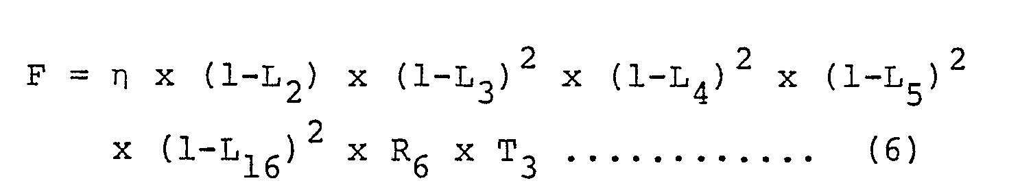

- When F is 1% - 10%, then T3 is 1.5 - 15% and the quarter wave plate is rotated by ±3.5° - 11.5°. At a standard feedback light factor of 2%, T3 is 3% and θ is 40° or 50° and the quarter wave plate is rotated by approximately ±5°.
- In the embodiment of Fig. 6b which uses two Brewster prisms, a similar calculation is carried out and the feedback light factor F of 1 - 10% is attained by T3 of 1.6 - 16%. The rotation angle of the quarter wave plate is substantially same as that when one Brewster prism is used, that is, ±3.5° - ±12° at the standard feedback light factor of 2%, T3 is 3.2% and the rotation angle of the quarter wave plate is ±5°.
- As discussed above, when the numerical aperture of the
coupling lens 2 is large, T3 is 1.5% for F = 1%. Thus, when the polarization beamsplitter is of relatively low precision, that is, it has an extinction ratio of approximately 1.5%, the feedback light factor of approximately 1% may be automatically attained even if the quarter wave plate is at the standard positioning angle, that is, 8 = 45°. However, it is resirable to rotate it by approximately 2% of the standard angle to give a margin. - When the
diffraction grating 10 shown in Fig. 5 is further inserted into the optical system having the Brewster prism, the transmission factor T3 of the polarization beamsplitter is determined by taking the 0-order light transmission factor TG 2 in both ways into consideration. - In the above embodiments, it is assumed that the
objective lens 5 facing the disc is fixed and the light loss in one way is 1%. In an actuator- operated system in which the objective lens can be moved in parallel to the disc plane for tracking servo, a diameter of theobjective lens 5 is reduced relative to a diameter of thecoupling lens 2 to allow the parallel movement. Accordingly, it is necessary to fully consider a light intensity reduction by a areal reduction. When the diameter of thecoupling lens 2 is 5.5 mm and the diameter of theobjective lens 5 is 4.3 mm, the output light intensity is approximately 0.6 times of the input light intensity. This should be taken into consideration of the above formula. - Thus far, the method for changing the transmission factor T3 of the polarization beamsplitter by' rotating the quarter wave plate around the optical axis of the optical system in order to attain the feedback light factor of 1 - 10% has been described. A desired T3 can also be attained by arranging the quarter wave plate obliquely to the incident light axis.
- An optical element having a phase shift preset to attain the desired T3 may be used in place of the quarter wave plate.
- When the order of arrangement in the system including the optical parts or the optical system is changed, the transmission factor T3 of the polarization beamsplitter is set by the quarter wave plate such that the feedback light factor to the emitting point is 1 - 10% in order to reduce the laser noise.
- When the quarter wave plate and the polarization beamsplitter are used, the signal light intensity is obtained with a relatively small laser output.
- A method which does not utilize the polarization of the laser beam in order to attain a desired feedback light factor is now explained.
- In an embodiment of Fig. 7, the
quarter wave plate 4 and thepolarization beamsplitter 3 of Fig. 1 are substituted by aprism 17 which is hardly subjected to an influence of the polarization and has specific transmission factor and reflection factor. Such an optical element is hereinafter referred to as a semi-transmissive prism. A desired feedback light factor is attained in the following manner. - T17 represents a transmission factor of the semi-transmissive prism to an incident light, and R17 represents a reflection factor. A sum of T17 and R17 is not necessarily unity because of absorption by the semi-transmissive prism. In general,
-

- The light emitted from the semiconductor laser I is collimated by the
coupling lens 2 and then applied to thesemi-transmissive prism 17. Only the T17 portion of the incident light transmits to the reflection plane and the R17 portion is deflected oppositely to thelight detector 7. As the light reflected by thereflection plane 6 reenters thesemi-transmissive prism 17, it is split into the transmission light and the reflection light and the light corresponding to_R17 reaches thelight detector 7 while the light corresponding to T17 is fed back to theemitting point 8. - Neglecting the loss of the semi-transmissive prism, that is, assuming that


- When F of 1 - 10% is desired, the transmission factor T17 of the semi-transmissive prism is selected to 22 - 77%. When F of 2% is desired, T3 is 34%. This is attained by setting the reflection factor R17 of the semi-transmissive prism to 66% and the transmission factor T17 to 34%.
-
Fi g. 8 shows an embodiment which uses a semi-transmissive prism. Thediffraction grating 10 and theconvex lens 11 of Fig. 5 are inserted in the pickup optical system. Assuming that a transmission factor TG of the 0-order light of thediffraction grating 10 is 70%, the feedback light factor is given by

- For F = 1%, T17 is 34%, and for F = 2%, T17 is 48%. In the latter case, a half-prism having substantially equal transmission factor and reflection factor can be used.
- Assuming that the
objective lens 5 can be moved in parallel to the disc and the light is attanuated by a factor of approximately 0.6 in theobjective lens 5, T17 is 63% for F = 2%. Thus, the semi-transmissive prism is designed to have the transmission factor of 63% and the reflection factor of 37%. - The
semi-transmissive prism 17 may be of one of various constructions. For example, the transmission and the reflection may be controlled by a certain metal film. It has a disadvantage that the light is absorbed by the metal film and hence the loss is high. An example of non-absorption construction is a dielectric multi-layer film. In general, the multi-layer construction is easy to control only for a certain polarization but difficult to control for the polarization normal thereto. Thus, when the multi-layer film prism is used, it is necessary to adjust the polarization direction of the laser. A distribution of retardation of the disc varies radially because material flow from the center to the periphery during the injection molding. Accordingly, the poralization parallel to a normal line of the disc track or tangential to the disc track is preferable. This is illustrated in Fig. 9. - Referring to Fig. 9, numeral 27 denotes information tracks on the disc. A
spot 28 scans in the direction of thetrack 27. The polarization direction is preferably parallel or perpendicular to thetrack 27 in the disc plane as shown by arrows a and b. In order to set the polarization direction relative to the track direction of the disc, the polarization direction of the semiconductor laser is set to a rotation angle parallel or normal in a plane normal to the optical axis. - In the embodiment of Fig. 8, a
light detector 25 is used to detect that portion of the light emitted from the laser which is first laterally deflected by the semi-transmissive prism in order to control a laser current. - In order to prevent the light transmitted through the plane 17b of the
semi-transmissive prism 17 from being reflected externally, applied again to the plane 17b and reaching thelight detector 7, the plane 17b may be a ground glass to scatter the light. For a similar purpose, the plane 17b may be inclined to prevent the light from returning to thelight detector 7. - While the present invention has been described in connection with the reflection type optical disc player, the present invention can also be applied to a transmission type optical disc player. Fig. 10a shows an embodiment of the present invention applied to the transmission type optical disc player. The light emitted from the
semiconductor laser 1 is focused to thespot 9 on the transmission type optical disc 6', and if an information pit exists there, the transmission light therefrom is detected by thelight sensor 7. In Fig. 10a, the feedback light to thesemiconductor laser 1 is attained by feeding back the light spot focused on areflection plane 18 other than the disc 6' to theemitting point 8. Assuming that the coupling efficiency n of thecoupling lens 2 is 20%, the reflector factor R18 of thereflection plane 18 is 90%, the loss L11 of theconvex lens 11 in one way is 1% and the reflection factor of thesemi-transmissive prism 17 is R17, the feedback light factor F is given by -


focal point 9 is on the disc 6' and afocal point 19 is exactly on thereflection plane 18. As shown in Fig. 10b, it is principally possible to eliminate thelens 11 and apply the light beam directly to thereflection plane 18. In this case, however, it is somewhat difficult to exactly feed back the light to theemitting point 8. - For the transmission type pickup, it is possible to control the feedback light by varying the reflection factor R18 of the
reflection plane 18. - So far, the system which uses the semi-transmissive prism has been described. As shown in Fig. 11, a semi-transmissive mirror plate may be used instead of the prism. In essence, the transmission factor or the reflection factor is controlled to feed back 1 - 10% of the total emitted light to the
emitting point 8 of the semiconductor laser. - When the semi-transmissive prism is used, the quarter wave plate is not necessary and hence a cost is reduced. Since the property of polarization is not utilized, the variation of the reflected light is reduced even if the disc includes the retardation.
- In the above description, the feedback light is obtained from the front of the semiconductor laser. It is also possible to obtain the feedback light from the rear of the semiconductor laser. Fig. 12 shows an embodiment in which a
lens 21 and asemi-transmissive mirror 22 are added to the optical system of Fig. 1 in order to feed back the rear light of thesemiconductor laser 1. Aspot 24 is formed by thelens 21 on the reflection plane of thesemi-transmissive mirror 22 and the reflected light therefrom is fed back to the rear emitting point 8'. The rear light of the semiconductor laser is usually used for monitoring to control the light output. In the present invention, this function is attained by detecting the transmitted light from thesemi-transmissive mirror 22 by thelight detector 23. Assuming that the numerical aperture of thelens 21 is 0.15, the coupling efficiency n' thereof is 20%, the reflection factor of thesemi-transmissive mirror 22 is R22 and the loss L21 of thelens 21 in the return path of the light is 1%, the feedback light factor F is given by -


semi-transmissive mirror 22 is selected to 5 - 50%. For the standard feedback light factor of 2%, R22 is selected to 10%. In this case, it is also necessary to adjust the optical system such that the laser beam is exactly focused on afocal point 24 on the reflection plane of thesemi-transmissive mirror 22. - When the feedback light is obtained from the rear light of the semiconductor laser, the front optical system such as the
polarization beamsplitter 3 and thequarter wave plate 4 may be identical to that of the prior art system. Accordingly, the utilization efficiency of the laser beam is maximized. The arrangement of Fig. 12 and the arrangement described above may be combined so that a desired feedback is attained by both the front light and the back light. - As described hereinabove, according to the present invention, the optical noise in the single longitudinal mode semiconductor laser is significantly reduced by feeding back 1% - 10% of the emitted light from the semiconductor laser to the emitting point of the semiconductor laser. As a result, a high quality of signal can be reproduced from the disc.
Claims (24)
Applications Claiming Priority (6)
| Application Number | Priority Date | Filing Date | Title |
|---|---|---|---|
| JP7572/82 | 1982-01-22 | ||
| JP57007572A JPS58125245A (en) | 1982-01-22 | 1982-01-22 | Optical pickup device |
| JP56581/82 | 1982-04-07 | ||
| JP57056581A JPS58175149A (en) | 1982-04-07 | 1982-04-07 | Optical pickup device |
| JP57070391A JPS58188342A (en) | 1982-04-28 | 1982-04-28 | Noise reducing method of semiconductor laser light |
| JP70391/82 | 1982-04-28 |
Publications (3)
| Publication Number | Publication Date |
|---|---|
| EP0084871A2 true EP0084871A2 (en) | 1983-08-03 |
| EP0084871A3 EP0084871A3 (en) | 1984-07-25 |
| EP0084871B1 EP0084871B1 (en) | 1988-03-30 |
Family
ID=27277661
Family Applications (1)
| Application Number | Title | Priority Date | Filing Date |
|---|---|---|---|
| EP83100531A Expired EP0084871B1 (en) | 1982-01-22 | 1983-01-21 | Method and apparatus for reducing semiconductor laser optical noise |
Country Status (3)
| Country | Link |
|---|---|
| US (1) | US4532619A (en) |
| EP (1) | EP0084871B1 (en) |
| DE (1) | DE3376172D1 (en) |
Cited By (4)
| Publication number | Priority date | Publication date | Assignee | Title |
|---|---|---|---|---|
| EP0167277A2 (en) * | 1984-06-01 | 1986-01-08 | Sharp Kabushiki Kaisha | A micro-displacement measuring apparatus |
| EP0176329A2 (en) * | 1984-09-24 | 1986-04-02 | Xerox Corporation | Laser diodes |
| EP0550929A1 (en) * | 1991-12-30 | 1993-07-14 | Koninklijke Philips Electronics N.V. | Optical device and apparatus for scanning an information plane, comprising such an optical device |
| US6205161B1 (en) | 1996-03-01 | 2001-03-20 | Agfa-Gevaert Aktiengesellschaft | Method and device for operating a laser diode |
Families Citing this family (31)
| Publication number | Priority date | Publication date | Assignee | Title |
|---|---|---|---|---|
| US5337302A (en) * | 1984-03-19 | 1994-08-09 | Ricoh Company, Ltd. | Optical data recording/reproduction apparatus for use with semiconductor lasers as a light source |
| KR920007294B1 (en) * | 1984-06-29 | 1992-08-29 | 가부시끼가이샤 히다찌세이사꾸쇼 | Optical head for magneto-optical memory |
| JPH0762913B2 (en) * | 1984-08-17 | 1995-07-05 | 株式会社日立製作所 | Automatic focus control method |
| JPH0693044B2 (en) * | 1985-03-22 | 1994-11-16 | 株式会社日立製作所 | Prism optical system and information device using the same |
| US4819242A (en) * | 1985-11-20 | 1989-04-04 | Hitachi, Ltd. | Semiconductor laser driver circuit |
| JPS63268139A (en) * | 1987-04-24 | 1988-11-04 | Alps Electric Co Ltd | Optical device for optical pickup |
| JPH0296622U (en) * | 1989-01-18 | 1990-08-01 | ||
| US5177346A (en) * | 1989-12-13 | 1993-01-05 | Computer Identics | Bar code reader system for reading bar code labels with a highly specular and low contrast surface |
| JPH05273491A (en) * | 1992-03-25 | 1993-10-22 | Toshiba Corp | Photodetector |
| US5940549A (en) * | 1996-07-30 | 1999-08-17 | Seagate Technology, Incorporated | Optical system and method using optical fibers for storage and retrieval of information |
| US6226233B1 (en) | 1996-07-30 | 2001-05-01 | Seagate Technology, Inc. | Magneto-optical system utilizing MSR media |
| US6850475B1 (en) * | 1996-07-30 | 2005-02-01 | Seagate Technology, Llc | Single frequency laser source for optical data storage system |
| US6574015B1 (en) | 1998-05-19 | 2003-06-03 | Seagate Technology Llc | Optical depolarizer |
| KR100480630B1 (en) * | 2002-11-13 | 2005-03-31 | 삼성전자주식회사 | Optical pickup capable of reducing noise and polarization changer |
| TWI256632B (en) * | 2004-05-18 | 2006-06-11 | Lite On It Corp | Optical power calibration fixture |
| US7667896B2 (en) * | 2004-05-27 | 2010-02-23 | Angstrom, Inc. | DVD recording and reproducing system |
| US7800823B2 (en) | 2004-12-06 | 2010-09-21 | Moxtek, Inc. | Polarization device to polarize and further control light |
| US7630133B2 (en) | 2004-12-06 | 2009-12-08 | Moxtek, Inc. | Inorganic, dielectric, grid polarizer and non-zero order diffraction grating |
| US7961393B2 (en) | 2004-12-06 | 2011-06-14 | Moxtek, Inc. | Selectively absorptive wire-grid polarizer |
| US20080055719A1 (en) * | 2006-08-31 | 2008-03-06 | Perkins Raymond T | Inorganic, Dielectric Grid Polarizer |
| US7570424B2 (en) | 2004-12-06 | 2009-08-04 | Moxtek, Inc. | Multilayer wire-grid polarizer |
| US8755113B2 (en) | 2006-08-31 | 2014-06-17 | Moxtek, Inc. | Durable, inorganic, absorptive, ultra-violet, grid polarizer |
| US7789515B2 (en) | 2007-05-17 | 2010-09-07 | Moxtek, Inc. | Projection device with a folded optical path and wire-grid polarizer |
| US8248696B2 (en) | 2009-06-25 | 2012-08-21 | Moxtek, Inc. | Nano fractal diffuser |
| US8913321B2 (en) | 2010-09-21 | 2014-12-16 | Moxtek, Inc. | Fine pitch grid polarizer |
| US8611007B2 (en) | 2010-09-21 | 2013-12-17 | Moxtek, Inc. | Fine pitch wire grid polarizer |
| US8913320B2 (en) | 2011-05-17 | 2014-12-16 | Moxtek, Inc. | Wire grid polarizer with bordered sections |
| US8873144B2 (en) | 2011-05-17 | 2014-10-28 | Moxtek, Inc. | Wire grid polarizer with multiple functionality sections |
| US8922890B2 (en) | 2012-03-21 | 2014-12-30 | Moxtek, Inc. | Polarizer edge rib modification |
| US9632223B2 (en) | 2013-10-24 | 2017-04-25 | Moxtek, Inc. | Wire grid polarizer with side region |
| JP6738254B2 (en) * | 2016-09-26 | 2020-08-12 | 株式会社日立ハイテク | Defect detection device and defect observation device |
Citations (2)
| Publication number | Priority date | Publication date | Assignee | Title |
|---|---|---|---|---|
| DE3027318A1 (en) * | 1979-08-03 | 1981-01-22 | Hitachi Ltd | OPTICAL SCANING SYSTEM |
| US4297651A (en) * | 1979-08-23 | 1981-10-27 | Northern Telecom Limited | Methods for simultaneous suppression of laser pulsations and continuous monitoring of output power |
Family Cites Families (5)
| Publication number | Priority date | Publication date | Assignee | Title |
|---|---|---|---|---|
| US4333173A (en) * | 1979-06-15 | 1982-06-01 | Hitachi, Ltd. | Optical information processor with prismatic correction of laser beam shape |
| FR2460523A1 (en) * | 1979-06-29 | 1981-01-23 | Thomson Csf | SEMICONDUCTOR LASER SOURCE OPTICAL READING HEAD AND DEVICE FOR REFLECTING AN INFORMATION MEDIUM COMPRISING SUCH AN OPTICAL HEAD |
| NL7907216A (en) * | 1979-09-28 | 1981-03-31 | Philips Nv | OPTICAL FOCUS ERROR DETECTION SYSTEM. |
| FR2470391A1 (en) * | 1979-11-21 | 1981-05-29 | Thomson Csf | STIGMATIC COHERENT RADIATION EMISSION-RECEPTION OPTICAL DEVICE AND RECORDING-READING OPTICAL HEAD COMPRISING SUCH A DEVICE |
| US4375680A (en) * | 1981-01-16 | 1983-03-01 | Mcdonnell Douglas Corporation | Optical acoustic sensor |
-
1983
- 1983-01-21 DE DE8383100531T patent/DE3376172D1/en not_active Expired
- 1983-01-21 EP EP83100531A patent/EP0084871B1/en not_active Expired
- 1983-01-21 US US06/460,015 patent/US4532619A/en not_active Expired - Lifetime
Patent Citations (2)
| Publication number | Priority date | Publication date | Assignee | Title |
|---|---|---|---|---|
| DE3027318A1 (en) * | 1979-08-03 | 1981-01-22 | Hitachi Ltd | OPTICAL SCANING SYSTEM |
| US4297651A (en) * | 1979-08-23 | 1981-10-27 | Northern Telecom Limited | Methods for simultaneous suppression of laser pulsations and continuous monitoring of output power |
Non-Patent Citations (5)
| Title |
|---|
| APPLIED PHYSICS LETTERS, vol. 33, no. 12, 15th December 1978, pages 990-992, American Institute of Physics, New York, US N.CHINONE et al.: "Stabilization of semiconductor laser outputs by a mirror close to a laser facet". * |
| APPLIED PHYSICS LETTERS, vol. 33, no. 12, 15th December 1978, pages 990-992, American Institute of Physics, New York, US; N. CHINONE et al.: "Stabilization of semiconductor laser outputs by a mirror close to a laser facet". * |
| ELECTRONICS LETTERS, vol. 17, no. 19, September 1981, pages 677-678, London, GB; L. GOLDBERG et al.: "Noise characteristics in line-narrowed semiconductor lasers with optical feedback". * |
| IEEE JOURNAL OF QUANTUM ELECTRONICS, vol. 15, no. 8, August 1979, New York, US; C.H.F. VELZEL et al.: "Output power and coherence length of stripe-geometry double-heterostructure semiconductor lasers in incoherent feedback". * |
| OPTICS COMMUNICATIONS, vol. 34, no. 3, September 1980, pages 309-310, Amsterdam, NL; Y. MITSUHASHI et al.: "Polarization-rotated optical feedback in self-coupled optical pickup". * |
Cited By (7)
| Publication number | Priority date | Publication date | Assignee | Title |
|---|---|---|---|---|
| EP0167277A2 (en) * | 1984-06-01 | 1986-01-08 | Sharp Kabushiki Kaisha | A micro-displacement measuring apparatus |
| EP0167277A3 (en) * | 1984-06-01 | 1987-09-30 | Sharp Kabushiki Kaisha | A micro-displacement measuring apparatus |
| EP0176329A2 (en) * | 1984-09-24 | 1986-04-02 | Xerox Corporation | Laser diodes |
| EP0176329A3 (en) * | 1984-09-24 | 1987-10-07 | Xerox Corporation | Laser diodes |
| EP0550929A1 (en) * | 1991-12-30 | 1993-07-14 | Koninklijke Philips Electronics N.V. | Optical device and apparatus for scanning an information plane, comprising such an optical device |
| US5333144A (en) * | 1991-12-30 | 1994-07-26 | U.S. Philips Corporation | Diode laser device having a reflecting feedback element, and apparatus using the device |
| US6205161B1 (en) | 1996-03-01 | 2001-03-20 | Agfa-Gevaert Aktiengesellschaft | Method and device for operating a laser diode |
Also Published As
| Publication number | Publication date |
|---|---|
| EP0084871B1 (en) | 1988-03-30 |
| EP0084871A3 (en) | 1984-07-25 |
| DE3376172D1 (en) | 1988-05-05 |
| US4532619A (en) | 1985-07-30 |
Similar Documents
| Publication | Publication Date | Title |
|---|---|---|
| EP0084871A2 (en) | Method and apparatus for reducing semiconductor laser optical noise | |
| US6154433A (en) | Light beam shaping device to change an anisotropic beam to an isotropic beam for reducing the size of an optical head | |
| US5278817A (en) | Optical pick-up for use with an opto-magnetic signal | |
| US4978187A (en) | Optical element, optical disc and rotary encoder with the optical element | |
| EP1001413B1 (en) | Optical pickup and optical device | |
| US5033040A (en) | Optical information recording and reproducing apparatus with tracking error control | |
| US5684779A (en) | Optical head with forward and reflected light beams propagating through a dual diffraction grating device along a common path | |
| US4945527A (en) | Optical pickup apparatus for detection of focusing error, tracking error, and information | |
| US5546373A (en) | Optical recording and/or reproducing apparatus including a two prism beam splitter for size reduction | |
| JPH11273119A (en) | Optical pickup device | |
| US5067117A (en) | Output stabilizing apparatus for an optical head | |
| US6327237B2 (en) | Optical pickup for recording or reproducing system | |
| US5598394A (en) | Optical pick-up | |
| US5708635A (en) | Ultra-resolving optical pickup device having an optical detector receiving an unfiltered reflected beam | |
| US6317400B1 (en) | Optical pickup apparatus | |
| US5073879A (en) | Information processing apparatus using a beam splitting means having non-polarization beam split surface | |
| US5761176A (en) | Optical head device with optically variable aperture for disks with different thicknesses | |
| JPS61162838A (en) | Driving device for light source of optical disk recording and reproducing device | |
| US5710753A (en) | Multi-element grating beam splitter using double refraction to reduce optical feedback and associated light source noise | |
| EP0537712B1 (en) | Optical pickup apparatus | |
| JP3526309B2 (en) | Optical information recording / reproducing device | |
| EP0747894A2 (en) | Optical head device with large tolerance to tilting | |
| JPH01307934A (en) | Optical head | |
| JPS5812143A (en) | Input and output device of optical information | |
| KR100266201B1 (en) | Optical pickup apparatus |
Legal Events
| Date | Code | Title | Description |
|---|---|---|---|
| PUAI | Public reference made under article 153(3) epc to a published international application that has entered the european phase |
Free format text: ORIGINAL CODE: 0009012 |
|
| AK | Designated contracting states |
Designated state(s): AT CH DE FR GB IT LI NL |
|
| PUAL | Search report despatched |
Free format text: ORIGINAL CODE: 0009013 |
|
| AK | Designated contracting states |
Designated state(s): AT CH DE FR GB IT LI NL |
|
| 17P | Request for examination filed |
Effective date: 19841214 |
|
| 17Q | First examination report despatched |
Effective date: 19860211 |
|
| GRAA | (expected) grant |
Free format text: ORIGINAL CODE: 0009210 |
|
| AK | Designated contracting states |
Kind code of ref document: B1 Designated state(s): DE GB |
|
| REF | Corresponds to: |
Ref document number: 3376172 Country of ref document: DE Date of ref document: 19880505 |
|
| PLBE | No opposition filed within time limit |
Free format text: ORIGINAL CODE: 0009261 |
|
| STAA | Information on the status of an ep patent application or granted ep patent |
Free format text: STATUS: NO OPPOSITION FILED WITHIN TIME LIMIT |
|
| 26N | No opposition filed | ||
| REG | Reference to a national code |
Ref country code: GB Ref legal event code: IF02 |
|
| PGFP | Annual fee paid to national office [announced via postgrant information from national office to epo] |
Ref country code: GB Payment date: 20020111 Year of fee payment: 20 |
|
| PGFP | Annual fee paid to national office [announced via postgrant information from national office to epo] |
Ref country code: DE Payment date: 20020226 Year of fee payment: 20 |
|
| PG25 | Lapsed in a contracting state [announced via postgrant information from national office to epo] |
Ref country code: GB Free format text: LAPSE BECAUSE OF EXPIRATION OF PROTECTION Effective date: 20030120 |
|
| REG | Reference to a national code |
Ref country code: GB Ref legal event code: PE20 Effective date: 20030120 |