EP0076082A2 - Display processing apparatus - Google Patents
Display processing apparatus Download PDFInfo
- Publication number
- EP0076082A2 EP0076082A2 EP82304960A EP82304960A EP0076082A2 EP 0076082 A2 EP0076082 A2 EP 0076082A2 EP 82304960 A EP82304960 A EP 82304960A EP 82304960 A EP82304960 A EP 82304960A EP 0076082 A2 EP0076082 A2 EP 0076082A2
- Authority
- EP
- European Patent Office
- Prior art keywords
- memory
- character
- data
- display
- character pattern
- Prior art date
- Legal status (The legal status is an assumption and is not a legal conclusion. Google has not performed a legal analysis and makes no representation as to the accuracy of the status listed.)
- Granted
Links
Images


Classifications
-
- G—PHYSICS
- G09—EDUCATION; CRYPTOGRAPHY; DISPLAY; ADVERTISING; SEALS
- G09G—ARRANGEMENTS OR CIRCUITS FOR CONTROL OF INDICATING DEVICES USING STATIC MEANS TO PRESENT VARIABLE INFORMATION
- G09G5/00—Control arrangements or circuits for visual indicators common to cathode-ray tube indicators and other visual indicators
- G09G5/22—Control arrangements or circuits for visual indicators common to cathode-ray tube indicators and other visual indicators characterised by the display of characters or indicia using display control signals derived from coded signals representing the characters or indicia, e.g. with a character-code memory
- G09G5/24—Generation of individual character patterns
- G09G5/26—Generation of individual character patterns for modifying the character dimensions, e.g. double width, double height
Definitions
- the present invention relates to a display processing apparatus, and more particularly to a display processing apparatus including memory means in which pattern information to be displayed is stored and means for addressing the memory means to select the pattern information to be displayed.
- a digital processor e. g. a microprocessor, a display controller
- a character pattern such as letters, digits, symbols, marks or figures
- a display device e. g. a CRT (cathode ray tube), LCD (liquid crystal display), and PDP (plasma display panel).
- Character pattern data to be displayed is preliminarily stored in a memory in the form of digital code and is read out of the memory by means of an addressing means of the digital processor.
- a read out character pattern data is sent to a display device, and is displayed at a designated position of a screen.
- Different types of signals are used in accordance with display devices for designating a position at which a character pattern is displayed.
- vertical and horizontal raster scanning signals are used in a CRT device, and digit and segment signals are used in an LCD device.
- digit and segment signals are used in an LCD device.
- these signals In order to accurately display a character pattern at a designated position of a screen, these signals must synchronize with a character pattern data to be sent to a display device. Therefore, it is preferred to easily couple with the memory and the display device.
- a character pattern data is stored in a memory so as to have a predetermined pattern size. Accordingly, the size of the character pattern is always constant on a screen. Change of its size is very difficult because of keeping aforementioned synchronous relation between the character pattern data and the signals for designating a position to be displayed. Consequently, the display processing apparatus of the prior art has the following shortcomings:
- Another object of the present invention is to provide a display processor which can arbitrarily set intervals between character rows.
- Still another object of the present invention is to provide a display processor which has a capability of arbitrarily changing in size of characters without increasing memory capacity, and which is especially effective to be formed as an integrated circuit.
- Yet another object of the present invention is to provide a display processor which can achieve magnification or reduction of characters without disturbing the synchronization between the timing of transfer of a character pattern data and the timing of display.
- a display processing apparatus comprising a memory for storing character data of a predetermined size, an addressing circuit for reading out predetermined character data from the memory by addressing, and a transfer circuit for transferring the read character data to a display circuit, in which the addressing circuit includes a first means for successively generating consecutive address data at a predetermined timing and a second means for generating non-consecutively varying address data.
- a ring counter is available as the first means.
- an arithmetic circuit for modifying the output of the ring counter may be used .
- operation processing for address data to be used for reading character data is effected. Accordingly, provided that the timing of read-out of character data is synchronized with the timing of display, even if the address data are modified, the synchronization would not be disturbed at all. Moreover, by modifying the address data it is possible to arbitrarily change the size of characters to be displayed. For instance, if the memory circuit is accessed by mapping only even number address or only odd number addresses among the consecutive address data, then characters reduced by a factor of can be displayed. On the other hand, by accessing a memory circuit while repeating every address n times (n being a positive integer), characters magnified by a factor of n can be displayed.
- first means and the second means could be coupled to each other so that either the consecutive address data derived from the first means may be passed in themselves through the second means and then applied to the memory or the consecutive address data may be modified in the second means and then applied to the memory.
- the address data can be easily modified by making use of a multiplier and an adder or a subtractor or the like according to necessity.
- the second means could be constructed of a combination of these arithmetic circuits. For instance, if the second means is constructed of a multiplier (X2), then among the addresses issued from the first means only the addresses at the even-numbered orders can be applied to the memory.
- the present invention is also easy to arbitrarily change the intervals in the vertical and/or horizontal direction between adjacent characters. Furthermore, since the present invention is equally applicable to either a display device having an interlacing function or non-interlacing function, the invention is excellent in its general usefulness.
- a display processor in the prior art will be described in detail with reference to a block diagram of an essential part thereof illustrated in Fig. 1.
- a group of letters, digits, symbols, figures, etc. are stored in a character generator (memory) .1 in a predetermined size.
- a controller 2 for controlling address outputs a character name address 6 and a row counter set signal 8 at predetermined timing, is shown in the diagram.
- a character “A” will be picked up and a dot-structure of the character “A” will be described with reference to Fig. 2.
- the character "A” is encoded within a dot matrix 10 of a predetermined size (for instance, 14 rows x 7 columns).
- Each dot D forming the matrix consists of a transistor element, a diode element, a fuse element or the like.
- setting of "0" or "1" serving as character data is effected by breakdown or non-breakdown of a junction or ON/OFF of a fuse element. Now it is assumed that in the dot matrix shown in Fig.
- the row counter 3 has a function of sequentially outputting the respective values 0 - 13, each of the output values is decoded by a row decoder 12 to sequentially generate row selection signals l 0 , l 1 , . , l 13 .
- the timing of outputting the respective row selection signals l 0 , l 1 , across,l 13 is synchronized with the horizontal scanning cycle of a CRT display screen.
- 7-dot data read out for every row are transferred in parallel to an output circuit 13, and then transferred to a parallel- serial converter 4 through a bus 7. After the 7-dot parallel data have been converted into serial data, they are sequencially transfered to a CRT display device.
- the size (meaning a number of dots) of the character that can be displayed on the CRT is coincident to the size (meaning a number of dots) of the character set within the character generator (that is, in the illustrated example 7 x 14). Accordingly, the number of character rows that can be displayed on the CRT display screen was necessarily fixed, and change of the number of character rows is difficult. Moreover, in such a display processor in the prior art, magnification or reduction in size of characters is also difficult. Furthermore, intervals in the vertical or horizontal direction between adjacent characters are predetermined, so that change of the intervals is difficult, too.
- Fig. 3 is a block diagram showing one preferred embodiment of the present invention.
- a character generator 20 is essentially a memory in which a group of letters, digits, symbols, figures, etc. are stored in the dot constructions as shown in Fig. 2.
- Each character name address is generated from a video RAM 22 and is input to the character generator 20 (in practice, to the column decoder shown in Fig. 2) through a bus 33.
- a CRT 31 for example, is used as a display device
- the character name addresses of all the characters to be displayed on one display screen of the CRT are edited along the scanning direction of horizontal scanning lines for one picture area.
- This edit is achieved by a controller 21 consisting of, for example, a microprocessor, and the edited character name addresses are written via a bus 32 into the video RAM 22 prior to the display. Furthermore, an output of a row counter 23 that is reset to its initial state by a control signal C fed from the controller 21, is subjected to operations as will be described later in a multiplier 24 and an adder 25, and the result of operations is applied via a bus 38 to the character generator 20 as a row selection address. In practice, the result is input to the row decoder shown in Fig. 2.
- the character name addresses as many as the number of characters that can be displayed in one row on the display screen of the CRT 32, in the sequence of display of the characters within every horizontal scanning cycle.
- the row selection address for the character generator 20, that is, the count data in the row counter 23 are not varied.
- the row selection address of the row counter 23 are varied each time one horizontal scanning line has been scanned.
- each character stored within the character generator 20 is constructed of a dot matrix of 14 rows x 7 columns. Then reference should be made to Fig. 2.
- an address designating the character "A” is output from the video RAM 22.
- the count in the counter 23 is "0".
- the controller 21 sets a multiplier factor "1" in the multiplier 24 via a bus 35 and an added factor "0" in the adder 25 via a bus 36
- the row selection address output from the row counter 23 is applied to the character generator 20 while being maintained at the same value as the count in the row counter 23.
- a character of the same size as the character "A" set in the character generator 20 is displayed on a screen through.scanning of 14 horizontal scanning lines as shown in Fig. 4.
- the row counter 23 is controlled by the controller 21 in such manner that when the count in the counter 23 has become “6", it may be detected by the controller 21 and in response thereto the counter 23 may be reset to "0", so that the counters in the counter 23 may change only within the range of "0" to "6".
- the size of the character to be displayed can be changed in a simple manner by modifying the output of the row counter 23 with the multiplier 24 and/or the adder 25.
- the character code data read out of the character generator 20 are converted into serial data 43 by means of a parallel-serial conversion shift register 29 and then output therefrom.
- the output data are input to a video signal generator 30, and an output video signal 40 is applied from the video signal generator 30 to the CRT 31.
- the comparator 26 includes a circuit for generating a start position signal 41 which indicates a display start position (a display start scanning line).
- the comparator 27 includes a circuit for generating an end position signal 42 which indicates a display end position (a display end scanning line).
- Data for comparison applied to the comparators 26 and 27 are sent from the controller 21 as data D and data D 2 , respectively. These data for comparison D and D 2 are compared at any arbitrary time with the count in the row counter 23, and if the count in the counter 23 coincides with the data D 1 , then a signal 41 for setting a flip-flop 28 is generated.
- a signal 42 for resetting the flip-flop 28 is generated.
- the parallel-serial conversion shift register 29 is controlled in such manner that it may be set when the flip-flop 28 has been set in the above-described fashion and it may be reset when the flip-flop 28 has been reset by the signal 42.
- the shift register 29 is set, data read out of the character generator 20 are allowed to be input to the shift register 29, whereas when it is reset, the data is inhibited from being input to the shift register 29.
- the controller 21 has set “2" in the comparator 26 as the data D 1 , and on the other hand it has set “9” in the comparator 27 as the data D 2 .
- the shift register 29 is activated for the first time, and when the count in the counter 23 has become “9”, the shift register 29 is reset, that is, inactivated.
- the addend in the adder 25 is set at "-3". In such a case, a subtractor could be employed instead of the adder.
- a similar interval equal to a width of two horizontal scanning lines can be provided under the character "A” by setting "0" and “7” in the comparators 26 and 27, respectively, and setting a multiplier factor "X2" in the multiplier 24 and an addend "+1" in the adder 25.
- a character as shown in Fig. 8 is displayed.
- the row counter 23 must be able to count 0 to 27, and only integer outputs must be sent from the multiplier 24 to the adder 25. That is, for the counts 0 to 27 of the row counter 23, the result of multiplication are 0, 0.5, 1, 1.5, 2, 2.5, 3 ...., 13, 13. 5. Accordingly, 0, 0, 1, 1, 2, 2, 3 ...., 13, 13 are input to the adder 25. This means that same address is repeated two times and is applied to the character generator 20. Therefore, a double size of character pattern shown in Fig. 8 is displayed on a screen.
- a divider may be employed instead of the multiplier 24.
- the adder 25 may be omitted.
- a size of a character pattern to be displayed can be easily changed without modifying a read-out character pattern data, so that the character pattern data transferred to tile CRT 31 can be easily synchronized with scanning signal of the CRT 31. For example, if 80 characters are displayed in one horizontal scanning period, a character name address must be changed 80 times in the same period, but a row address from the row counter 23 may not be changed. Therefore, the present invention can easily and accurately change a size of a character pattern by modifying the row address.
- the above-described control can be achieved regardless of whether the scanning system of the CRT 31 is an interlace system or not.
- the maximum value of the row counter is set at "13”
- the multiplier factor in the multiplier 24 is set at "X2" and the addend in the adder 25 is set at "+0"
- control can be effected in such manner that the displayed character pattern may be erased gradually from its bottom, that is, in the rder of the row selection addresses 13, 12, .... , 0, starting from the bottom row selection address 13.
- Such mode of control for erasing has an advantage that as compared to momentary erasing of a displayed pattern, the erasing of the pattern can be more distinctly impressed in the operator's mind.
Abstract
Description
- The present invention relates to a display processing apparatus, and more particularly to a display processing apparatus including memory means in which pattern information to be displayed is stored and means for addressing the memory means to select the pattern information to be displayed.
- Heretofore, a digital processor (e. g. a microprocessor, a display controller) has been used for the purpose of displaying a character pattern (such as letters, digits, symbols, marks or figures) on a display device, e. g. a CRT (cathode ray tube), LCD (liquid crystal display), and PDP (plasma display panel). Character pattern data to be displayed is preliminarily stored in a memory in the form of digital code and is read out of the memory by means of an addressing means of the digital processor. A read out character pattern data is sent to a display device, and is displayed at a designated position of a screen. Different types of signals are used in accordance with display devices for designating a position at which a character pattern is displayed. For instance, vertical and horizontal raster scanning signals are used in a CRT device, and digit and segment signals are used in an LCD device. In order to accurately display a character pattern at a designated position of a screen, these signals must synchronize with a character pattern data to be sent to a display device. Therefore, it is preferred to easily couple with the memory and the display device.
- On the other hand, a character pattern data is stored in a memory so as to have a predetermined pattern size. Accordingly, the size of the character pattern is always constant on a screen. Change of its size is very difficult because of keeping aforementioned synchronous relation between the character pattern data and the signals for designating a position to be displayed. Consequently, the display processing apparatus of the prior art has the following shortcomings:
- 1 . Since the change in size of a character pattern on a display screen is impossible, increase or decrease of a number of character patterns which can be displayed on a screen is also impossible.
- 2. Since intervals between vertically or horizontally consecutive characters cannot be changed, in the case where especially complexed characters appear consecutively to each other, it is difficult to identify the respective characters.
- 3. In order to display a character pattern with a different size, another memory in which a character pattern data according to the size is prepared is additionally necessitated; and therefore, memory capacity is greatly increased.
- 4. It is indeed possible to provide a circuit having a high degree of operation capability such as function operations between a memory and a display device so that character data read out of the memory may be input to that circuit to carry out magnification or reduction of character size through extremely complex operations. However, this circuit is very complex and is very expensive. In addition, although the timing of read-out of character data and the timing of display on a screen can be synchronized in a relatively simple manner, in the above-mentioned modified case since the operations must be effected between the memory and the display device, the synchronization between the timing of read-out and the timing of display becomes hard to achieve. Accordingly, flickering or deviation of display is liable to occur.
- It is therefore one object of the present invention to provide a display processing apparatus which has a capability of simply controlling change in size of character pattern.
- Another object of the present invention is to provide a display processor which can arbitrarily set intervals between character rows.
- Still another object of the present invention is to provide a display processor which has a capability of arbitrarily changing in size of characters without increasing memory capacity, and which is especially effective to be formed as an integrated circuit.
- Yet another object of the present invention is to provide a display processor which can achieve magnification or reduction of characters without disturbing the synchronization between the timing of transfer of a character pattern data and the timing of display.
- According to one feature of the present invention, there is provided a display processing apparatus comprising a memory for storing character data of a predetermined size, an addressing circuit for reading out predetermined character data from the memory by addressing, and a transfer circuit for transferring the read character data to a display circuit, in which the addressing circuit includes a first means for successively generating consecutive address data at a predetermined timing and a second means for generating non-consecutively varying address data.
- For instance, a ring counter is available as the first means. As the second means, an arithmetic circuit for modifying the output of the ring counter may be used .
- In the preferred embodiment instead of carrying out operation processing for character data, operation processing for address data to be used for reading character data is effected. Accordingly, provided that the timing of read-out of character data is synchronized with the timing of display, even if the address data are modified, the synchronization would not be disturbed at all. Moreover, by modifying the address data it is possible to arbitrarily change the size of characters to be displayed. For instance, if the memory circuit is accessed by mapping only even number address or only odd number addresses among the consecutive address data, then characters reduced by a factor of can be displayed. On the other hand, by accessing a memory circuit while repeating every address n times (n being a positive integer), characters magnified by a factor of n can be displayed.
- Furthermore, the first means and the second means could be coupled to each other so that either the consecutive address data derived from the first means may be passed in themselves through the second means and then applied to the memory or the consecutive address data may be modified in the second means and then applied to the memory. The address data can be easily modified by making use of a multiplier and an adder or a subtractor or the like according to necessity. The second means could be constructed of a combination of these arithmetic circuits. For instance, if the second means is constructed of a multiplier (X2), then among the addresses issued from the first means only the addresses at the even-numbered orders can be applied to the memory. In addition, as will be described later, in the preferred embodiment it is also easy to arbitrarily change the intervals in the vertical and/or horizontal direction between adjacent characters. Furthermore, since the present invention is equally applicable to either a display device having an interlacing function or non-interlacing function, the invention is excellent in its general usefulness.
- The above-mentioned and other objects, features and advantages of the present invention will become more apparent by reference to the following description of a preferred embodiment of the invention taken in conjunction with the accompanying drawings:
- Fig. 1 is a block diagram of an essential part of a display processing apparatus in the prior art;
- Fig.2 is a block diagram showing a dot-construction of one character within a memory and connecting relations between the memory and an address decoder and an output circuit;
- Fig.3 is a block diagram showing a display processing apparatus according to one preferred embodiment of the present invention; and
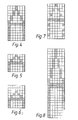
- Fig. 4 to 8 are illustrations of different display patterns for same one character processed in different manners by the display processor shown in Fig. 3.
- A display processor in the prior art will be described in detail with reference to a block diagram of an essential part thereof illustrated in Fig. 1. A group of letters, digits, symbols, figures, etc. are stored in a character generator (memory) .1 in a predetermined size. A
controller 2 for controlling address outputs acharacter name address 6 and a row counter setsignal 8 at predetermined timing, is shown in the diagram. - Now one character stored within the character generator 1, for example, a character "A" will be picked up and a dot-structure of the character "A" will be described with reference to Fig. 2. The character "A" is encoded within a
dot matrix 10 of a predetermined size (for instance, 14 rows x 7 columns). Each dot D forming the matrix consists of a transistor element, a diode element, a fuse element or the like. In general, setting of "0" or "1" serving as character data is effected by breakdown or non-breakdown of a junction or ON/OFF of a fuse element. Now it is assumed that in the dot matrix shown in Fig. 2, in the dot represented by a blanked square is stored a datum "0", and in the dot represented by a hatched square is stored a datum "I". When acharacter name address 6 designating the character "A" is output from thecontroller 2 in Fig. 2, it is decoded by acolumn decoder 11 so that selection signals r 0 - r6 may be generated simultaneously in parallel to select thematrix 10. As a result, the character "A" is selected, and reading of the character is executed by a row address applied from a row counter 3. The row counter 3 has a function of sequentially outputting the respective values 0 - 13, each of the output values is decoded by arow decoder 12 to sequentially generate row selection signals ℓ0, ℓ1, ....., ℓ13. The timing of outputting the respective row selection signals ℓ0, ℓ1,.....,ℓ13 is synchronized with the horizontal scanning cycle of a CRT display screen. 7-dot data read out for every row are transferred in parallel to anoutput circuit 13, and then transferred to a parallel- serial converter 4 through abus 7. After the 7-dot parallel data have been converted into serial data, they are sequencially transfered to a CRT display device. - As will be seen from the above explanation, the size (meaning a number of dots) of the character that can be displayed on the CRT is coincident to the size (meaning a number of dots) of the character set within the character generator (that is, in the illustrated example 7 x 14). Accordingly, the number of character rows that can be displayed on the CRT display screen was necessarily fixed, and change of the number of character rows is difficult. Moreover, in such a display processor in the prior art, magnification or reduction in size of characters is also difficult. Furthermore, intervals in the vertical or horizontal direction between adjacent characters are predetermined, so that change of the intervals is difficult, too.
- In this connection, although a display processor having a capability of displaying characters in a magnified or reduced size has been proposed in the prior art, the display processor necessitated to additionally provide a memory (character generator) for magnified display or for reduced display, hence increase of the memory capacity was immeasurable and the display processor had an extremely high cost. Further, if an arithmetic circuit is inserted between the character generator 1 and the converter 4 to change a character size, it becomes very hard to synchronize with a character pattern data and a display timing signal.
- Fig. 3 is a block diagram showing one preferred embodiment of the present invention. A
character generator 20 is essentially a memory in which a group of letters, digits, symbols, figures, etc. are stored in the dot constructions as shown in Fig. 2. Each character name address is generated from avideo RAM 22 and is input to the character generator 20 (in practice, to the column decoder shown in Fig. 2) through abus 33. In the case where aCRT 31, for example, is used as a display device, in thevideo RAM 22 the character name addresses of all the characters to be displayed on one display screen of the CRT are edited along the scanning direction of horizontal scanning lines for one picture area. This edit is achieved by acontroller 21 consisting of, for example, a microprocessor, and the edited character name addresses are written via abus 32 into thevideo RAM 22 prior to the display. Furthermore, an output of arow counter 23 that is reset to its initial state by a control signal C fed from thecontroller 21, is subjected to operations as will be described later in amultiplier 24 and anadder 25, and the result of operations is applied via abus 38 to thecharacter generator 20 as a row selection address. In practice, the result is input to the row decoder shown in Fig. 2. - In this case, from the
video RAM 22 are sequentially output the character name addresses as many as the number of characters that can be displayed in one row on the display screen of theCRT 32, in the sequence of display of the characters within every horizontal scanning cycle. On the other hand, in each horizontal scanning cycle, the row selection address for thecharacter generator 20, that is, the count data in therow counter 23 are not varied. The row selection address of therow counter 23 are varied each time one horizontal scanning line has been scanned. - Now it is assumed that each character stored within the
character generator 20 is constructed of a dot matrix of 14 rows x 7 columns. Then reference should be made to Fig. 2. In the case of displaying a character "A" as illustrated in Fig. 2, an address designating the character "A" is output from thevideo RAM 22. At this moment, the count in thecounter 23 is "0". Thecontroller 21 sets a multiplier factor "1" in themultiplier 24 via abus 35 and an added factor "0" in theadder 25 via abus 36 Accordingly, the row selection address output from therow counter 23 is applied to thecharacter generator 20 while being maintained at the same value as the count in therow counter 23. As a result, a character of the same size as the character "A" set in thecharacter generator 20 is displayed on a screen through.scanning of 14 horizontal scanning lines as shown in Fig. 4. - On the other hand, if it is desired to reduce the size of the characters to be displayed by a factor of 1/2 in the vertical direction, then a multiplier factor "X2" and an added factor "+1" are set in the
multiplier 24 and theadder 25, respectively. Consequently, in response to a series of output counts "0, 1, 2, 3, .... " from therow counter 23, a series of odd numbers "1, 3, 5, 7, .... " are output from theadder 25. Accordingly, only the coded data in the odd-numbered rows are selected and are displayed as shown in Fig. 5. Here, it will be seen that the size of the displayed character has been reduced by a factor of 1/2 in the vertical direction. It is to be noted that in the case of the above-mentioned reduced display, therow counter 23 is controlled by thecontroller 21 in such manner that when the count in thecounter 23 has become "6", it may be detected by thecontroller 21 and in response thereto thecounter 23 may be reset to "0", so that the counters in thecounter 23 may change only within the range of "0" to "6". - In this way, the size of the character to be displayed can be changed in a simple manner by modifying the output of the row counter 23 with the
multiplier 24 and/or theadder 25. It is to be noted that the character code data read out of thecharacter generator 20 are converted intoserial data 43 by means of a parallel-serial conversion shift register 29 and then output therefrom. The output data are input to avideo signal generator 30, and anoutput video signal 40 is applied from thevideo signal generator 30 to theCRT 31. - Furthermore, display positions of characters can be arbitrarily changed by adding
comparators comparator 26 includes a circuit for generating astart position signal 41 which indicates a display start position (a display start scanning line). - Likewise, thecomparator 27 includes a circuit for generating anend position signal 42 which indicates a display end position (a display end scanning line). Data for comparison applied to thecomparators controller 21 as data D and data D2, respectively. These data for comparison D and D2 are compared at any arbitrary time with the count in therow counter 23, and if the count in thecounter 23 coincides with the data D1, then asignal 41 for setting a flip-flop 28 is generated. On the other hand, if the count in thecounter 23 coincides with the data D2, then asignal 42 for resetting the flip-flop 28 is generated. The parallel-serial conversion shift register 29 is controlled in such manner that it may be set when the flip-flop 28 has been set in the above-described fashion and it may be reset when the flip-flop 28 has been reset by thesignal 42. When the shift register 29 is set, data read out of thecharacter generator 20 are allowed to be input to the shift register 29, whereas when it is reset, the data is inhibited from being input to the shift register 29. - It is assumed, by way of example, that the
controller 21 has set "2" in thecomparator 26 as the data D1, and on the other hand it has set "9" in thecomparator 27 as the data D2. Under such condition, when the count in therow counter 23 has become "2", the shift register 29 is activated for the first time, and when the count in thecounter 23 has become "9", the shift register 29 is reset, that is, inactivated. It is assumed that during this operation the addend in theadder 25 is set at "-3". In such a case, a subtractor could be employed instead of the adder. If the count operation of therow counter 23 is commenced under the above-mentioned condition, then character data are not output from thecharacter generator 20 during the period when the count in therow counter 23 is "0" or "I", and hence theCRT 31 is in a non-display condition. Subsequently, when the count in therow counter 23 has become "2", the flip-flop 28 is set, and so, the shift register 29 is set in a ready-to-receive condition for the input data. At that time, if a multiplier factor "X2" has been already set in themultiplier 24, then the resultant row selection address becomes (2 x 2 - 3) = 1, and hence data stored in the row ℓ1 in Fig. 2 are output from thecharacter generator 20. As a result, on theCRT 31, the data corresponding to the row f of the character "A" is displayed for the first time on the third horizontal scanning line. Subsequently, each time the count in therow counter 23 is changed in the sequence of 3, 4, 5, 6, 7 and 8, the row selecticn address applied to thecharacter generator 20 is changed in the sequence of 3, 5, 7, 9, 11 and 13, and therefore, the same pattern as that shown in Fig. 5 is displayed on theCRT 31. Further, when the count in therow counter 23 has become "9", the flip-flop 28 is reset by the output of thecomparator 27, so that the parallel-serial conversion shift register 29 rejects to receive the subsequent input data. Accordingly, as shown in Fig. 6, two scanning lines above the character "A" form a non-display region, and in this way an interval between vertically adjacent characters can be provided. - It is to be noted that a similar interval equal to a width of two horizontal scanning lines can be provided under the character "A" by setting "0" and "7" in the
comparators multiplier 24 and an addend "+1" in theadder 25. - Further, when a multiplier factor "X½" and an added factor "+0" are set in the
multiplier 24 and theadder 25, respectively, a character as shown in Fig. 8 is displayed. In this case, therow counter 23 must be able to count 0 to 27, and only integer outputs must be sent from themultiplier 24 to theadder 25. That is, for thecounts 0 to 27 of therow counter 23, the result of multiplication are 0, 0.5, 1, 1.5, 2, 2.5, 3 ...., 13, 13. 5. Accordingly, 0, 0, 1, 1, 2, 2, 3 ...., 13, 13 are input to theadder 25. This means that same address is repeated two times and is applied to thecharacter generator 20. Therefore, a double size of character pattern shown in Fig. 8 is displayed on a screen. A divider may be employed instead of themultiplier 24. Of course, theadder 25 may be omitted. - It may thus be seen that a size of a character pattern to be displayed can be easily changed without modifying a read-out character pattern data, so that the character pattern data transferred to tile
CRT 31 can be easily synchronized with scanning signal of theCRT 31. For example, if 80 characters are displayed in one horizontal scanning period, a character name address must be changed 80 times in the same period, but a row address from therow counter 23 may not be changed. Therefore, the present invention can easily and accurately change a size of a character pattern by modifying the row address. - Obviously, the above-described control can be achieved regardless of whether the scanning system of the
CRT 31 is an interlace system or not. Especially in a CRT of the scanning type not employing the interlace system, since a pattern is displayed only on alternate horizontal scanning lines, if the maximum value of the row counter is set at "13" , the multiplier factor in themultiplier 24 is set at "X2" and the addend in theadder 25 is set at "+0", it is possible to read out only the data stored in the odd-numbered rows (ℓ1, ℓ3.... 913) of the character generator in Fig. 2 and display then only on the even-numbered horizontal scanning lines in the displayed character pattern, as shown in Fig. 7. - Furthermore, with respect to the character "A" displayed on the display screen, if the value of the comparison data D2 set in the
comparator 27 is decreased one by one from its maximum value in the successive frame cycles as synchronized with the frame scanning after the character "A" has been once displayed, then control can be effected in such manner that the displayed character pattern may be erased gradually from its bottom, that is, in the rder of the row selection addresses 13, 12, .... , 0, starting from the bottomrow selection address 13. Such mode of control for erasing has an advantage that as compared to momentary erasing of a displayed pattern, the erasing of the pattern can be more distinctly impressed in the operator's mind. - In addition, even if modification should be made such that row selection addresses may be applied from the
video RAM 22 to thecharacter generator 20 and column selection addresses may be derived from the count in thecounter 23 through themultiplier 24 and theadder 25 and then applied to thecharacter generator 20, similar effects and advantages could be expected. Furthermore, the constructions of thecomparators comparator 26 may detect the condition of (the count in the counter 23] > D1, while thecomparator 27 may detect the condition of [the count in the counter 23] < D2, and an AND gate is provided in place of the flip-flop 28.
Claims (3)
Applications Claiming Priority (2)
| Application Number | Priority Date | Filing Date | Title |
|---|---|---|---|
| JP56149157A JPS5850589A (en) | 1981-09-21 | 1981-09-21 | Display processor |
| JP149157/81 | 1981-09-21 |
Publications (3)
| Publication Number | Publication Date |
|---|---|
| EP0076082A2 true EP0076082A2 (en) | 1983-04-06 |
| EP0076082A3 EP0076082A3 (en) | 1984-08-22 |
| EP0076082B1 EP0076082B1 (en) | 1987-07-29 |
Family
ID=15469030
Family Applications (1)
| Application Number | Title | Priority Date | Filing Date |
|---|---|---|---|
| EP82304960A Expired EP0076082B1 (en) | 1981-09-21 | 1982-09-21 | Display processing apparatus |
Country Status (4)
| Country | Link |
|---|---|
| US (1) | US4630039A (en) |
| EP (1) | EP0076082B1 (en) |
| JP (1) | JPS5850589A (en) |
| DE (1) | DE3276882D1 (en) |
Cited By (4)
| Publication number | Priority date | Publication date | Assignee | Title |
|---|---|---|---|---|
| US4581721A (en) * | 1981-11-18 | 1986-04-08 | Texas Instruments Incorporated | Memory apparatus with random and sequential addressing |
| EP0261629A2 (en) * | 1986-09-20 | 1988-03-30 | Minolta Camera Kabushiki Kaisha | Display apparatus |
| EP0284326A2 (en) * | 1987-03-25 | 1988-09-28 | Fujitsu Limited | Pattern display signal generating apparatus and display apparatus using the same |
| GB2273426A (en) * | 1992-12-14 | 1994-06-15 | Motorola Inc | Programmable character size |
Families Citing this family (19)
| Publication number | Priority date | Publication date | Assignee | Title |
|---|---|---|---|---|
| JPS5970547A (en) * | 1982-10-15 | 1984-04-21 | Mitsubishi Heavy Ind Ltd | Method and apparatus for manufacturing radial tire |
| JPS60130791A (en) * | 1983-12-19 | 1985-07-12 | シャープ株式会社 | Control system for character generator |
| EP0383367B1 (en) * | 1983-12-26 | 1999-03-17 | Hitachi, Ltd. | Graphic pattern processing apparatus and method |
| US4814760A (en) * | 1984-12-28 | 1989-03-21 | Wang Laboratories, Inc. | Information display and entry device |
| JPH0762794B2 (en) * | 1985-09-13 | 1995-07-05 | 株式会社日立製作所 | Graphic display |
| US6697070B1 (en) | 1985-09-13 | 2004-02-24 | Renesas Technology Corporation | Graphic processing system |
| US4887813A (en) * | 1986-10-14 | 1989-12-19 | Amf Bowling, Inc. | Bowling scoring display system |
| US4821031A (en) * | 1988-01-20 | 1989-04-11 | International Computers Limited | Image display apparatus |
| US5562350A (en) * | 1988-04-18 | 1996-10-08 | Canon Kabushiki Kaisha | Output apparatus that selects a vector font based on character size |
| US5255185A (en) * | 1988-04-18 | 1993-10-19 | Brunswick Bowling & Billiards Corp. | Bowling center video display system |
| JP2613933B2 (en) * | 1988-12-02 | 1997-05-28 | 株式会社 日立製作所 | Display capacity conversion device and display system |
| US5243332A (en) * | 1991-10-31 | 1993-09-07 | Massachusetts Institute Of Technology | Information entry and display |
| US5400051A (en) * | 1992-11-12 | 1995-03-21 | International Business Machines Corporation | Method and system for generating variably scaled digital images |
| WO1995026022A1 (en) * | 1994-03-18 | 1995-09-28 | Tally Display Corp. | Display system |
| US5521614A (en) * | 1994-04-29 | 1996-05-28 | Cirrus Logic, Inc. | Method and apparatus for expanding and centering VGA text and graphics |
| JP3413432B2 (en) * | 1994-05-30 | 2003-06-03 | 富士ゼロックス株式会社 | Character expansion processor |
| JPH08153189A (en) * | 1994-11-28 | 1996-06-11 | Nec Niigata Ltd | Optionally magnification varying device for digital image |
| US5724067A (en) * | 1995-08-08 | 1998-03-03 | Gilbarco, Inc. | System for processing individual pixels to produce proportionately spaced characters and method of operation |
| US6281876B1 (en) * | 1999-03-03 | 2001-08-28 | Intel Corporation | Method and apparatus for text image stretching |
Citations (4)
| Publication number | Priority date | Publication date | Assignee | Title |
|---|---|---|---|---|
| DE2213953A1 (en) * | 1972-03-22 | 1973-09-27 | Siemens Ag | CIRCUIT ARRANGEMENT FOR DISPLAYING CHARACTERS ON THE SCREEN OF A DISPLAY DEVICE |
| US4107786A (en) * | 1976-03-01 | 1978-08-15 | Canon Kabushiki Kaisha | Character size changing device |
| FR2423018A1 (en) * | 1978-04-14 | 1979-11-09 | Fujitsu Fanuc Ltd | CHARACTER DISPLAY DEVICE |
| US4284989A (en) * | 1976-06-21 | 1981-08-18 | Texas Instruments Incorporated | Character display apparatus with facility for selectively expanding the height of displayed characters |
Family Cites Families (8)
| Publication number | Priority date | Publication date | Assignee | Title |
|---|---|---|---|---|
| US3474438A (en) * | 1965-09-30 | 1969-10-21 | Monsanto Co | Display system |
| US3903517A (en) * | 1974-02-26 | 1975-09-02 | Cummins Allison Corp | Dual density display |
| US3999168A (en) * | 1974-11-11 | 1976-12-21 | International Business Machines Corporation | Intermixed pitches in a buffered printer |
| JPS587997B2 (en) * | 1974-12-25 | 1983-02-14 | 松下電器産業株式会社 | Zukeishingou Hatsuseisouchi |
| JPS51129141A (en) * | 1975-05-06 | 1976-11-10 | Toshiba Corp | Character enlargement display system |
| JPS526419A (en) * | 1975-07-07 | 1977-01-18 | Fuji Xerox Co Ltd | Dot matrix convertor |
| JPS5416931A (en) * | 1977-07-07 | 1979-02-07 | Nec Corp | Magnified character display system for cathode-ray tube display unit |
| US4168489A (en) * | 1978-02-13 | 1979-09-18 | Lexitron Corp. | Full page mode system for certain word processing devices |
-
1981
- 1981-09-21 JP JP56149157A patent/JPS5850589A/en active Granted
-
1982
- 1982-09-21 US US06/420,676 patent/US4630039A/en not_active Expired - Lifetime
- 1982-09-21 EP EP82304960A patent/EP0076082B1/en not_active Expired
- 1982-09-21 DE DE8282304960T patent/DE3276882D1/en not_active Expired
Patent Citations (4)
| Publication number | Priority date | Publication date | Assignee | Title |
|---|---|---|---|---|
| DE2213953A1 (en) * | 1972-03-22 | 1973-09-27 | Siemens Ag | CIRCUIT ARRANGEMENT FOR DISPLAYING CHARACTERS ON THE SCREEN OF A DISPLAY DEVICE |
| US4107786A (en) * | 1976-03-01 | 1978-08-15 | Canon Kabushiki Kaisha | Character size changing device |
| US4284989A (en) * | 1976-06-21 | 1981-08-18 | Texas Instruments Incorporated | Character display apparatus with facility for selectively expanding the height of displayed characters |
| FR2423018A1 (en) * | 1978-04-14 | 1979-11-09 | Fujitsu Fanuc Ltd | CHARACTER DISPLAY DEVICE |
Cited By (6)
| Publication number | Priority date | Publication date | Assignee | Title |
|---|---|---|---|---|
| US4581721A (en) * | 1981-11-18 | 1986-04-08 | Texas Instruments Incorporated | Memory apparatus with random and sequential addressing |
| EP0261629A2 (en) * | 1986-09-20 | 1988-03-30 | Minolta Camera Kabushiki Kaisha | Display apparatus |
| EP0261629A3 (en) * | 1986-09-20 | 1989-10-11 | Minolta Camera Kabushiki Kaisha | Display apparatus |
| EP0284326A2 (en) * | 1987-03-25 | 1988-09-28 | Fujitsu Limited | Pattern display signal generating apparatus and display apparatus using the same |
| EP0284326B1 (en) * | 1987-03-25 | 1993-02-03 | Fujitsu Limited | Pattern display signal generating apparatus and display apparatus using the same |
| GB2273426A (en) * | 1992-12-14 | 1994-06-15 | Motorola Inc | Programmable character size |
Also Published As
| Publication number | Publication date |
|---|---|
| US4630039A (en) | 1986-12-16 |
| EP0076082B1 (en) | 1987-07-29 |
| JPS5850589A (en) | 1983-03-25 |
| JPS6261277B2 (en) | 1987-12-21 |
| DE3276882D1 (en) | 1987-09-03 |
| EP0076082A3 (en) | 1984-08-22 |
Similar Documents
| Publication | Publication Date | Title |
|---|---|---|
| EP0076082B1 (en) | Display processing apparatus | |
| US4200869A (en) | Data display control system with plural refresh memories | |
| US4668947A (en) | Method and apparatus for generating cursors for a raster graphic display | |
| JPH04106593A (en) | Still image display device | |
| CA1220293A (en) | Raster scan digital display system | |
| US5142363A (en) | Method and apparatus for scaling interlaced images | |
| EP0178897B1 (en) | Display apparatus | |
| US4607340A (en) | Line smoothing circuit for graphic display units | |
| JPS59160174A (en) | Graphic display unit | |
| EP0238232A2 (en) | Video memory control device | |
| JPS6155119B2 (en) | ||
| GB2055027A (en) | Displaying alphanumeric data | |
| EP0420281B1 (en) | Luminance interpolation type waveform display apparatus | |
| EP0399136A2 (en) | Display apparatus | |
| JPS6150318B2 (en) | ||
| JP2609628B2 (en) | Memory address controller | |
| JPS63245084A (en) | Interlace picture data conversion system | |
| JPS6261156B2 (en) | ||
| JP3009088B2 (en) | Scan format converter | |
| JP2647073B2 (en) | Graphic display device | |
| JPS6350706Y2 (en) | ||
| JPH04354069A (en) | Picture processor | |
| JPH04186293A (en) | Image processing system | |
| JPS5890691A (en) | Pattern generator | |
| JPH073439B2 (en) | Waveform display device |
Legal Events
| Date | Code | Title | Description |
|---|---|---|---|
| PUAI | Public reference made under article 153(3) epc to a published international application that has entered the european phase |
Free format text: ORIGINAL CODE: 0009012 |
|
| AK | Designated contracting states |
Designated state(s): DE FR GB |
|
| RAP1 | Party data changed (applicant data changed or rights of an application transferred) |
Owner name: NEC CORPORATION |
|
| PUAL | Search report despatched |
Free format text: ORIGINAL CODE: 0009013 |
|
| AK | Designated contracting states |
Designated state(s): DE FR GB |
|
| 17P | Request for examination filed |
Effective date: 19841108 |
|
| 17Q | First examination report despatched |
Effective date: 19860130 |
|
| GRAA | (expected) grant |
Free format text: ORIGINAL CODE: 0009210 |
|
| AK | Designated contracting states |
Kind code of ref document: B1 Designated state(s): DE FR GB |
|
| ET | Fr: translation filed | ||
| REF | Corresponds to: |
Ref document number: 3276882 Country of ref document: DE Date of ref document: 19870903 |
|
| PLBE | No opposition filed within time limit |
Free format text: ORIGINAL CODE: 0009261 |
|
| STAA | Information on the status of an ep patent application or granted ep patent |
Free format text: STATUS: NO OPPOSITION FILED WITHIN TIME LIMIT |
|
| 26N | No opposition filed | ||
| PGFP | Annual fee paid to national office [announced via postgrant information from national office to epo] |
Ref country code: FR Payment date: 20010911 Year of fee payment: 20 |
|
| PGFP | Annual fee paid to national office [announced via postgrant information from national office to epo] |
Ref country code: GB Payment date: 20010919 Year of fee payment: 20 |
|
| PGFP | Annual fee paid to national office [announced via postgrant information from national office to epo] |
Ref country code: DE Payment date: 20011009 Year of fee payment: 20 |
|
| REG | Reference to a national code |
Ref country code: GB Ref legal event code: IF02 |
|
| PG25 | Lapsed in a contracting state [announced via postgrant information from national office to epo] |
Ref country code: GB Free format text: LAPSE BECAUSE OF EXPIRATION OF PROTECTION Effective date: 20020920 |
|
| REG | Reference to a national code |
Ref country code: GB Ref legal event code: PE20 Effective date: 20020920 |