EP0065396A2 - DC-AC converter - Google Patents
DC-AC converter Download PDFInfo
- Publication number
- EP0065396A2 EP0065396A2 EP82302343A EP82302343A EP0065396A2 EP 0065396 A2 EP0065396 A2 EP 0065396A2 EP 82302343 A EP82302343 A EP 82302343A EP 82302343 A EP82302343 A EP 82302343A EP 0065396 A2 EP0065396 A2 EP 0065396A2
- Authority
- EP
- European Patent Office
- Prior art keywords
- inverter
- output
- waveform
- fundamental frequency
- clock
- Prior art date
- Legal status (The legal status is an assumption and is not a legal conclusion. Google has not performed a legal analysis and makes no representation as to the accuracy of the status listed.)
- Withdrawn
Links
Images


Classifications
-
- H—ELECTRICITY
- H02—GENERATION; CONVERSION OR DISTRIBUTION OF ELECTRIC POWER
- H02M—APPARATUS FOR CONVERSION BETWEEN AC AND AC, BETWEEN AC AND DC, OR BETWEEN DC AND DC, AND FOR USE WITH MAINS OR SIMILAR POWER SUPPLY SYSTEMS; CONVERSION OF DC OR AC INPUT POWER INTO SURGE OUTPUT POWER; CONTROL OR REGULATION THEREOF
- H02M7/00—Conversion of ac power input into dc power output; Conversion of dc power input into ac power output
- H02M7/42—Conversion of dc power input into ac power output without possibility of reversal
- H02M7/44—Conversion of dc power input into ac power output without possibility of reversal by static converters
- H02M7/48—Conversion of dc power input into ac power output without possibility of reversal by static converters using discharge tubes with control electrode or semiconductor devices with control electrode
- H02M7/53—Conversion of dc power input into ac power output without possibility of reversal by static converters using discharge tubes with control electrode or semiconductor devices with control electrode using devices of a triode or transistor type requiring continuous application of a control signal
- H02M7/537—Conversion of dc power input into ac power output without possibility of reversal by static converters using discharge tubes with control electrode or semiconductor devices with control electrode using devices of a triode or transistor type requiring continuous application of a control signal using semiconductor devices only, e.g. single switched pulse inverters
- H02M7/5387—Conversion of dc power input into ac power output without possibility of reversal by static converters using discharge tubes with control electrode or semiconductor devices with control electrode using devices of a triode or transistor type requiring continuous application of a control signal using semiconductor devices only, e.g. single switched pulse inverters in a bridge configuration
- H02M7/53871—Conversion of dc power input into ac power output without possibility of reversal by static converters using discharge tubes with control electrode or semiconductor devices with control electrode using devices of a triode or transistor type requiring continuous application of a control signal using semiconductor devices only, e.g. single switched pulse inverters in a bridge configuration with automatic control of output voltage or current
- H02M7/53875—Conversion of dc power input into ac power output without possibility of reversal by static converters using discharge tubes with control electrode or semiconductor devices with control electrode using devices of a triode or transistor type requiring continuous application of a control signal using semiconductor devices only, e.g. single switched pulse inverters in a bridge configuration with automatic control of output voltage or current with analogue control of three-phase output
Definitions
- This invention relates generally to apparatus and methods for converting direct current to alternating current using pulse width modulation to reduce the magnitude of undesirable harmonics.
- variable speed motor drive systems use the pulse width modulation (PWM) method to achieve the necessary control characteristics.
- PWM pulse width modulation
- One of the disadvantages associated with operating a variable frequency multiphase inverter using PWM techniques is an increase in the magnitudes of undesirable harmonics in the output waveforms.
- the presence of undesirable harmonics in the output waveform is particularly important in the lower range of the operating frequency spectrum wherein such harmonics usually increase in amplitude compared with the amplitude of the fundamental frequency component created under such conditions.
- the prior art contains many examples of pulse width modulated power sources capable of producing various waveforms.
- the "six-step" waveform is the basic waveform of many prior art inverters.
- the conventional six-step waveform results from switching each of the three legs of a three-phase inverter twice in each wavelength of the output fundamental frequency. A sequence of switching actions occurs with a phase difference of 60 degrees separating the switching action in each leg from the switching in the other two legs. The potential differences between pairs of legs of the inverter produce the three-phase output waveforms. While it is generally accepted that the six-step wave is satisfactory for energising an A.C. motor, modulation of the six-step waveform for variable frequency A.C. motor drive systems produces outputs which are relatively high in harmonic content.
- a second method for minimising undesirable harmonics in the output of an inverter system while modulating the fundamental frequency component is to introduce additional switching actions into the inverter to produce notches in the output waveforms.
- the placement and control of auxiliary switching points has been the subject of considerable investigation which has produced numerous switching systems.
- the goal of each system is to minimise the number of inverter switching actions consistent with the capability to control the amplitude of the fundamental frequency component and harmonic content over a wide operating frequency range.
- motor losses due to fifth and seventh harmonics has heretofore remained a serious difficulty in variable frequency A.C. motor drive systems.
- the art exhibits a need for a low-cost, efficient inverter system which produces a variable frequency output having a constant voltage to frequency ratio in the fundamental frequency and having acceptable fifth and seventh harmonic frequency components.
- an inverter comprises a direct current source (10) of electrical energy, a plurality of switch means (14,15, 16) connected to the direct current source; drive means (22,23,24) for selectively actuating the switch means; a clock (32) for generating clock signals (6A) having a clock frequency which is a multiple of a predetermined fundamental frequency; interval timer means (28,30) responsive to the clock signals for generating synchronised intervals (44,46) of predetermined duration; and a drive control (26) responsive to the synchronised intervals and the clock signals for controlling the drive means to produce a pulse width modulated output at the fundamental frequency but with notches corresponding to the synchronised intervals.
- each cycle eight extra points are used in addition to the two necessary for generating a basic six step waveform. These eight additional switching points are placed within each wave length such that notches in the waveform which result therefrom are created symmetrically about the 75 0 , 105°, 255°, and 285° points. Controlling the width of the notches in all three legs of a three-phase inverter controls the amplitude of the fundamental frequency component of the output waveform. The particular angles which are the centres of the notches create a unique relationship between the fundamental frequency component and the fifth and the seventh harmonics. As the notches become symmetrically wider, the amplitude of the fundamental frequency component linearly decreases.
- this decrease in the amplitude of the fundamental is accompanied by a decrease in the amplitude of the fifth and seventh harmonic frequency components, which both decrease at a rate more rapid than that of the fundamental frequency component as the notches become wider. Therefore, as the notch width increases, the fifth and seventh harmonic frequency components represent decreasing portions of the total waveform.
- the waveforms which are the output of the invention, when applied to an A.C. induction motor drive system or to any appropriate load, permit variable frequency, constant volts/Hertz operation without increasing the percentages of fifth and seventh harmonics above that present in the basic six-step waveform.
- the present invention permits implementation by simple, low-cost digital logic components.
- the invention includes a method for converting direct current into polyphase alternating current, comprising the steps of; connecting a plurality of switching means to a direct current source of electrical energy; selectively actuating said switching means for selected periods of time with a gating means output to produce output waveforms having a fundamental frequency in each of a plurality of phases; varying said selected periods of time to control the percentage of selected harmonics in said output waveform in each phase; and maintaining the ratio of voltage to fundamental frequency in the output waveform at a substantially constant value in each phase.
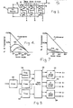
- an inverter for providing a three phase A.C. output includes a D.C. source 10 which provides a D.C. input into a switch network 12, which comprises a first group of switches A+, B+ and C+ connected to the positive terminal of DC source 10 and a second group of switches A-, Band C- connected to the negative terminal of DC source 10.
- Switch network 12 is a basic version of a three phase inverter bridge with switches A+ and A- connected together to form a leg 14 thereof and with switches B+ and B-, C+ and C- being similarly connected to form a leg 15 and a leg 16, respectively.
- Switch network 12 includes an A.C. output terminal A connected to a junction 18 between switches A+ and A-; an A.C.
- Switch network 12 thus provides a three phase output having a phase AB taken between output terminals A and B, a phase BC taken between output terminals B and C, and a phase CA taken between output terminals C and A.
- switches A+, A-, B+,B-C+ and C- are transistors and a base drive circuit 21 has outputs connected to the bases of the transistors for controlling the switching actions thereof.
- FIG. 2 illustrates the waveforms which result from conventional operation of switch network 12 to produce six step waveforms.
- the condition of each of pair switches A+, A-; B+, B-; and C+, C- changes every 180° of the output fundamental frequency.
- the switching of each pair is separated by 60° from each of the other pairs.
- One switch of each pair is closed while the counterpart thereof is open to produce predetermined phase relationships between the A.C. output signals at output terminals A, B, and C.
- the waveforms A, .B and ..C represent line-to-neutral voltages for the three output terminals A, B, and C, respectively, wherein the neutral is the midpoint of the D.C. input potential.
- Waveforms D, E and F represent the line-to-line voltages between the output phases AB, BC, and CA, respectively.
- the waveforms representing line-to-line voltages are each the difference between a pair of line-to-neutral waveforms.
- the waveform D representing the line voltage of output phase AB is the difference between voltage waveforms A and B.
- the line-to-line waveforms have twice the amplitude of the line-to-neutral waveforms and alternate from positive to negative in the form of pulses which extend for 120° in a normal three phase system.
- the line-to-line waveform AB has a 60° zero amplitude portion which results either when switches A+ and B+ are connected to the positive terminal of the DC source or when switches A- and B- are connected to the negative terminal of the DC source.
- Line-to-line voltage waveforms BC and CA are similar to line-to-line voltage waveform AB with the only differences being phase shifts of 120° and 240°, respectively.
- Fig. 3 illustrates typical waveforms which result from pulse width modulation of the six step waveform with waveforms 3A-3F corresponding to waveforms 2A-2F.
- pulse width modulation involves "notching" a rectangular pulse to produce a modulated output waveform.
- notching as used herein with respect to a waveform means to change the state of the waveform for a predetermined period of time during each cycle thereof so as to cause a notch or gap to appear in the waveform.
- leg 14 For example, the switching of leg 14 so that switch A+ is on and switch A- is off between 240° and 270° and switching leg 14 so that switch A- is on and switch A+ is off between 60° and 90°, as shown in waveform 3A produces a notch 36 in pulse 38 of waveform 3D and a notch 40 in pulse 42 thereof.
- the duration of a notch in the output line-to-line waveforms is hereinafter referred to as the notch angle.
- pulse width modulation by introducing notches into a rectangular waveform may substantially eliminate lower order harmonics; but, as shown in Fig. 4, higher order harmonics, such as the fifth and seventh, may become appreciable fractions of the amplitude of the fundamental frequency component of the waveform.
- Fig. 4 represents the percentages of the fundamental amplitude of the fifth and seventh harmonics as functions of the notch angle.
- the illustrated amplitudes of the fifth and seventh harmonics are such proportions of the fundamental amplitude that driving a motor with such a waveform would result in severe motor losses due to the relatively high percentage of harmonic content.
- the present invention utilizes a gating circuit for the inverter system which includes an A phase driver 22 having output terminals A+ and A-, a B phase driver 23 having output terminals B+ and B-, and a C phase driver 24 having output terminals C+ and C-.
- Phase drivers 22-24 comprise suitable switching devices, which are connected to the bases of the transistors A+, A-, B+, B-, C+, C- to control the switching action thereof.
- the circuitry which controls the switching action of the phase drivers 22-24 includes a gate matrix 26, a first interval timer 28, a second interval timer 30, a clock 32 and a ring counter 34.
- Clock 32 which includes means for varying the frequency of the clock pulses, provides clock output signals to interval timer 28 and to ring counter 34.
- Interval timer 28 outputs a signal to interval timer 30 and to gate matrix 26; and both timers 28 and 30 and ring counter 34 provide control signals to gate matrix 26, which provides switch control signals to each of the phase drivers 22-24.
- Interval timers 28 and 30 each include therein means for adjusting the duration of the output signals thereof.
- Fig. 6 illustrates the output signals of clock 32 (6A), ring counter 34 (6B-6M), interval timer 28 (6N), interval timer 30 (6P), gate matrix 26 (6Q), phase drivers 22-24 (6R-6T), and the line-to-line output voltages AB (6V), BC (6V), and CA (6W).
- the circuitry of Fig. 5 performs eight switching operations in each of the phase drivers 22-24 in addition to the two switching operations necessary in each for generating the basic six step waveform of Fig. 3 to produce a variable frequency output waveform having a constant ratio of voltage to frequency with acceptable fifth and seventh harmonic content.
- the frequency of the clock signal 6A which is input to interval timer 28 and ring counter 34, is twelve times the fundamental frequency of the output line-to-line waveform.
- ring counter 34 produces a succession of 12 pulses 6B-6M, each having a duration equal to the time interval between successive clock pulses.
- interval timer 28 produces a sequence of pulses 6N indicative of a first selected time interval.
- the falling edge 44 of each pulse output from interval timer 28 triggers interval timer 30 to produce a train of pulses 6P indicative of a second selected time interval such that the rising edge 46 of each pulse output of interval timer 30 is in substantial alignment with the falling edge of each interval timer 28 pulse.
- the output pulses of interval timer 30 and interval timer 28 have durations of 7.5°.
- the rising and falling edges of the pulses output from ring counter 34 and interval timers 28 and 30 control gate matrix 26 to produce a succession of gate matrix pulses 6Q for controlling the switching action of the phase drivers 22-24.
- the output of gate matrix 26 combines sets of 3 very short pulses 7.5° apart with 15° between successive sets of pulses, with information from the ring counter pulses, 6B-6M, to activate the appropriate driver.
- the preferred embodiment described herein includes interval timers28 and 30 for controlling notch width, those skilled in the relevant arts should recognize that any method for producing waveforms 6N and 6P, which control the switching actions of the gate matrix 26, could be used in implementing the present invention.
- the 0° reference of Fig. 6 corresponds to the 0° reference of Fig. 2 for the basic six step waveform.
- Gate matrix 26 produces an output'pulse at 0° to switch the output waveform 6R of A phase driver 22 from negative to positive to initiate a positive rectangular pulse 48 at output terminal A of Fig 1.
- Gate matrix 26 produces an output pulse at 67.5° to switch A phase driver 22 from positive to negative; and a gate matrix pulse at 82.5° switches the output of A phase driver 22 from negative to positive to form a notch 50 in the output of A phase driver 22.
- Notch 50 is centered about the 75° point in the output waveform of A phase driver 22 and has a notch angle of 15°.
- a gate matrix pulse at 97.5° switches the output of A phase driver 22 from positive to negative; and a gate matrix pulse at 112.5° switches the output of A phase driver 22 from negative to positive to form a second notch 52 in the output waveform of A phase driver 22.
- Notch 52 also has a notch angle of 15° and is centered about the 105° point in the waveform 6R.
- the switching action in A phase driver 22 at the 112.5° point initiates a positive pulse 54, which terminates at the 180° point to begin a negative rectangular pulse 56 as in the basic six step waveform.
- a gate matrix pulse at 247.5° switches the output of A phase driver 22 from negative to positive
- a gate matrix pulse at 262.5° switches the output of A phase driver 22 from positive to negative to form a notch 58 centered about the 255° point in the waveform 6R with a notch angle of 15°.
- a phase driver 22 produces a negative rectangular pulse 60 which terminates upon the occurrence of a gate matrix pulse at 277.5°, at which time the output waveform 6R of A phase driver 22 switches from negative to positive.
- the output of A phase driver 22 switches from positive to negative at 292.5° to form a notch 62 centered about the 285 * point with a notch angle of 15°.
- a negative rectangular pulse 64 completes the remainder of the wavelength of the waveform 6R.
- the remaining gate matrix pulses 6Q cause B phase driver 23 and C phase driver 24 to undergo switching operations similar to those of A phase driver 22 to produce a B phase driver output waveform 6S and a C phase driver output waveform 6T.
- the output waveforms of B phase driver 23 and C phase driver 24 have the same configuration as the output waveform of A phase driver 22 with phase lags of 120° and 240°, respectively, relative to the output waveform of A phase driver 22.
- Waveform 6U illustrates the line-to-line voltage AB, which is the potential difference between the output terminals A and B of Fig. 1.
- output waveform 6U is the difference between waveform 6R and waveform 6S.
- Waveform 6U begins at 0° with a positive pulse 66 having a duration of 7.5° followed by a null signal 68 having a duration of 15°.
- Waveform 6U continues with three positive rectangular pulses 70, 72 and 74, each having a 15° duration with a 15° null signal 76 between pulses 70 and 72 and a 15° null signal 78 between pulses 72 and 74.
- a 15° null signal 80 separates a 7.5° rectangular pulse 82 from pulse 74.
- null signal 84 From the 120° point to the 180° point waveform 6U is a null signal 84. Beginning at 180°, the waveform continues with a succession of pulses which are the negatives of the pulses 66, 70, 72, 74 and 82 with 15° null signals separating adjacent pulses. From 300° to 360° the output waveform 6U is a null signal 86.
- Waveform 6V represents the potential difference between B phase driver 23 and C phase driver 24; and waveform 6W represents the potential difference between C phase driver 24 and A phase driver 22.
- the waveforms 6V and 6W have the same configuration as waveform 6U but have phase lags of 120° and 240°, respectively relative to waveform 6U.
- Fig. 7 illustrates the relationship of the fundamental frequency component and the fifth and seventh harmonics as functions of the notch angles located in each phase as described hereinabove. Varying the notch angles modulates the amplitude of the fundamental frequency component in the line-to-line output voltage waveforms because increasing the notch angle decreases the magnitude of the fundamental frequency component.
- circuitry which controls the locations and notch angles provides means for controlling the amplitude of the fundamental frequency component of the output waveform and the percentages of fifth and seventh harmonics therein.
- Adjustment of the duration of the pulses output from interval timers 28 and 30 sets a specific volts/Hertz value over the entire operating frequency. Timers 28 and 30 may be adjusted at any time during operation of the system to provide voltage compensation, current limiting, or programmed changes of the volts/Hertz ratio.
Landscapes
- Engineering & Computer Science (AREA)
- Power Engineering (AREA)
- Inverter Devices (AREA)
- Ac-Ac Conversion (AREA)
Abstract
A pulse width modulated three-phase inverter has notches (50, 52) in the output waveforms (R.S.T.) to control the harmonic content thereof, the width of which notches are variable (at 28,30) in accordance with load requirements.
Description
- This invention relates generally to apparatus and methods for converting direct current to alternating current using pulse width modulation to reduce the magnitude of undesirable harmonics.
- Many direct current to alternating current inverter systems use pulse width modulation to control both single phase and polyphase outputs. There is increasing use of solid state inverters for control elements, particularly in applications to variable frequency A.C. motor drive systems. One of the desirable characteristics of an inverter drive system for such an application is the ability to maintain constant motor torque over a relatively wide motor speed range, which requires that the A.C. motor energising potential display a substantially constant ratio of voltage to frequency as the frequency varies. Most solid state controls maintain a fixed ratio of voltage to frequency by either controlling the D.C. input to a fixed pulse width inverter or by controlling the inverter output pulse width as a function of frequency and using a substantially constant voltage source of D.C. energy.
- Because the first method mentioned usually involves two stages of power control, recent variable speed motor drive systems use the pulse width modulation (PWM) method to achieve the necessary control characteristics. One of the disadvantages associated with operating a variable frequency multiphase inverter using PWM techniques is an increase in the magnitudes of undesirable harmonics in the output waveforms. The presence of undesirable harmonics in the output waveform is particularly important in the lower range of the operating frequency spectrum wherein such harmonics usually increase in amplitude compared with the amplitude of the fundamental frequency component created under such conditions.
- The prior art contains many examples of pulse width modulated power sources capable of producing various waveforms. The "six-step" waveform is the basic waveform of many prior art inverters. The conventional six-step waveform results from switching each of the three legs of a three-phase inverter twice in each wavelength of the output fundamental frequency. A sequence of switching actions occurs with a phase difference of 60 degrees separating the switching action in each leg from the switching in the other two legs. The potential differences between pairs of legs of the inverter produce the three-phase output waveforms. While it is generally accepted that the six-step wave is satisfactory for energising an A.C. motor, modulation of the six-step waveform for variable frequency A.C. motor drive systems produces outputs which are relatively high in harmonic content. It is possible to use PWM to control the amplitude of the fundamental frequency component of a six-step waveform; however, as the amplitude of the fundamental frequency component decreases, the amplitudes of the fifth and seventh harmonics, which are the most undesirable, increase to such portions of the total waveform that motor losses severely penalize the effectiveness of the system.
- In the prior art, the effects of increasing amplitudes of the fifth and seventh harmonics are minimised by using a multiple inverter system and combining the outputs of the inverters such that the undesirable harmonics are substantially eliminated. Multiple inverter systems usually introduce considerable complexity and cost into the inverter equipment.
- A second method for minimising undesirable harmonics in the output of an inverter system while modulating the fundamental frequency component is to introduce additional switching actions into the inverter to produce notches in the output waveforms. The placement and control of auxiliary switching points has been the subject of considerable investigation which has produced numerous switching systems. In general, the goal of each system is to minimise the number of inverter switching actions consistent with the capability to control the amplitude of the fundamental frequency component and harmonic content over a wide operating frequency range. However, motor losses due to fifth and seventh harmonics has heretofore remained a serious difficulty in variable frequency A.C. motor drive systems.
- The art exhibits a need for a low-cost, efficient inverter system which produces a variable frequency output having a constant voltage to frequency ratio in the fundamental frequency and having acceptable fifth and seventh harmonic frequency components.
- According to the invention, an inverter comprises a direct current source (10) of electrical energy, a plurality of switch means (14,15, 16) connected to the direct current source; drive means (22,23,24) for selectively actuating the switch means; a clock (32) for generating clock signals (6A) having a clock frequency which is a multiple of a predetermined fundamental frequency; interval timer means (28,30) responsive to the clock signals for generating synchronised intervals (44,46) of predetermined duration; and a drive control (26) responsive to the synchronised intervals and the clock signals for controlling the drive means to produce a pulse width modulated output at the fundamental frequency but with notches corresponding to the synchronised intervals.
- In a preferred form in each cycle eight extra points are used in addition to the two necessary for generating a basic six step waveform. These eight additional switching points are placed within each wave length such that notches in the waveform which result therefrom are created symmetrically about the 750, 105°, 255°, and 285° points. Controlling the width of the notches in all three legs of a three-phase inverter controls the amplitude of the fundamental frequency component of the output waveform. The particular angles which are the centres of the notches create a unique relationship between the fundamental frequency component and the fifth and the seventh harmonics. As the notches become symmetrically wider, the amplitude of the fundamental frequency component linearly decreases. However, this decrease in the amplitude of the fundamental is accompanied by a decrease in the amplitude of the fifth and seventh harmonic frequency components, which both decrease at a rate more rapid than that of the fundamental frequency component as the notches become wider. Therefore, as the notch width increases, the fifth and seventh harmonic frequency components represent decreasing portions of the total waveform.
- The waveforms, which are the output of the invention, when applied to an A.C. induction motor drive system or to any appropriate load, permit variable frequency, constant volts/Hertz operation without increasing the percentages of fifth and seventh harmonics above that present in the basic six-step waveform. In addition to providing acceptable fifth and seventh harmonics as the fundamental frequency varies, the present invention permits implementation by simple, low-cost digital logic components.
- The invention includes a method for converting direct current into polyphase alternating current, comprising the steps of; connecting a plurality of switching means to a direct current source of electrical energy; selectively actuating said switching means for selected periods of time with a gating means output to produce output waveforms having a fundamental frequency in each of a plurality of phases; varying said selected periods of time to control the percentage of selected harmonics in said output waveform in each phase; and maintaining the ratio of voltage to fundamental frequency in the output waveform at a substantially constant value in each phase.
-
- Fig. 1 is a simplified schematic diagram of an inverter system;
- Fig. 2 is a series of waveform diagrams labeled A- F corresponding to the conventional operation of the inverter of Fig. 1;
- Fig. 3 is a series of waveform diagrams labeled A- F for pulse width modulated operation of the inverter of Fig. 1;
- Fig. 4 is a graph illustrating harmonics related to the inverter system of Fig. 1 operated to produce the waveform of Fig. 3;
- Fig. 5 is a block diagram of a gating circuit for use in the inverter system of Fig. 1 according to the present invention;
- Fig. 6 is a series of waveforms for the inverter system of Fig. 1 having the gating circuitry of Fig. 5; and
- Fig. 7 is a graph illustrating harmonics related to the inverter system of this invention.
- Referring to Fig. 1, an inverter for providing a three phase A.C. output includes a
D.C. source 10 which provides a D.C. input into aswitch network 12, which comprises a first group of switches A+, B+ and C+ connected to the positive terminal ofDC source 10 and a second group of switches A-, Band C- connected to the negative terminal ofDC source 10.Switch network 12 is a basic version of a three phase inverter bridge with switches A+ and A- connected together to form aleg 14 thereof and with switches B+ and B-, C+ and C- being similarly connected to form aleg 15 and aleg 16, respectively.Switch network 12 includes an A.C. output terminal A connected to ajunction 18 between switches A+ and A-; an A.C. output terminal B connected to ajunction 19 between switches B+ and B-; and an AC output terminal C connected to a junction 20 between switches C+ and C-.Switch network 12 thus provides a three phase output having a phase AB taken between output terminals A and B, a phase BC taken between output terminals B and C, and a phase CA taken between output terminals C and A. - In the illustrated embodiment the switches A+, A-, B+,B-C+ and C- are transistors and a
base drive circuit 21 has outputs connected to the bases of the transistors for controlling the switching actions thereof. - Operation of the circuit of Fig. 1 will be described with reference to Fig. 2 which illustrates the waveforms which result from conventional operation of
switch network 12 to produce six step waveforms. The condition of each of pair switches A+, A-; B+, B-; and C+, C- changes every 180° of the output fundamental frequency. The switching of each pair is separated by 60° from each of the other pairs. One switch of each pair is closed while the counterpart thereof is open to produce predetermined phase relationships between the A.C. output signals at output terminals A, B, and C. The waveforms A, .B and ..C represent line-to-neutral voltages for the three output terminals A, B, and C, respectively, wherein the neutral is the midpoint of the D.C. input potential. - Waveforms D, E and F represent the line-to-line voltages between the output phases AB, BC, and CA, respectively. The waveforms representing line-to-line voltages are each the difference between a pair of line-to-neutral waveforms. For example, the waveform D representing the line voltage of output phase AB is the difference between voltage waveforms A and B. The line-to-line waveforms have twice the amplitude of the line-to-neutral waveforms and alternate from positive to negative in the form of pulses which extend for 120° in a normal three phase system. The line-to-line waveform AB has a 60° zero amplitude portion which results either when switches A+ and B+ are connected to the positive terminal of the DC source or when switches A- and B- are connected to the negative terminal of the DC source.
- Line-to-line voltage waveforms BC and CA are similar to line-to-line voltage waveform AB with the only differences being phase shifts of 120° and 240°, respectively.
- Previous attempts to use pulse width modulation of the basic six step waveform illustrated in Fig. 2 to provide a variable frequency signal having a constant voltage-to-frequency ratio have resulted in the increased percentage of undesirable harmonics in the output waveform. Fig. 3 illustrates typical waveforms which result from pulse width modulation of the six step waveform with waveforms 3A-3F corresponding to waveforms 2A-2F. In inverter applications, pulse width modulation involves "notching" a rectangular pulse to produce a modulated output waveform. The term "notching" as used herein with respect to a waveform means to change the state of the waveform for a predetermined period of time during each cycle thereof so as to cause a notch or gap to appear in the waveform. For example, the switching of
leg 14 so that switch A+ is on and switch A- is off between 240° and 270° and switchingleg 14 so that switch A- is on and switch A+ is off between 60° and 90°, as shown in waveform 3A produces anotch 36 inpulse 38 of waveform 3D and a notch 40 in pulse 42 thereof. The duration of a notch in the output line-to-line waveforms is hereinafter referred to as the notch angle. - It is known in the art that pulse width modulation by introducing notches into a rectangular waveform may substantially eliminate lower order harmonics; but, as shown in Fig. 4, higher order harmonics, such as the fifth and seventh, may become appreciable fractions of the amplitude of the fundamental frequency component of the waveform. Fig. 4 represents the percentages of the fundamental amplitude of the fifth and seventh harmonics as functions of the notch angle. The illustrated amplitudes of the fifth and seventh harmonics are such proportions of the fundamental amplitude that driving a motor with such a waveform would result in severe motor losses due to the relatively high percentage of harmonic content.
- Referring to Fig. 5, the present invention utilizes a gating circuit for the inverter system which includes an
A phase driver 22 having output terminals A+ and A-, aB phase driver 23 having output terminals B+ and B-, and aC phase driver 24 having output terminals C+ and C-. Phase drivers 22-24 comprise suitable switching devices, which are connected to the bases of the transistors A+, A-, B+, B-, C+, C- to control the switching action thereof. The circuitry which controls the switching action of the phase drivers 22-24 includes agate matrix 26, afirst interval timer 28, asecond interval timer 30, aclock 32 and aring counter 34. -
Clock 32, which includes means for varying the frequency of the clock pulses, provides clock output signals tointerval timer 28 and to ringcounter 34.Interval timer 28 outputs a signal tointerval timer 30 and togate matrix 26; and bothtimers ring counter 34 provide control signals togate matrix 26, which provides switch control signals to each of the phase drivers 22-24.Interval timers - Operation of the circuit of Fig. 5 can be understood with reference to Fig. 6 which illustrates the output signals of clock 32 (6A), ring counter 34 (6B-6M), interval timer 28 (6N), interval timer 30 (6P), gate matrix 26 (6Q), phase drivers 22-24 (6R-6T), and the line-to-line output voltages AB (6V), BC (6V), and CA (6W). The circuitry of Fig. 5 performs eight switching operations in each of the phase drivers 22-24 in addition to the two switching operations necessary in each for generating the basic six step waveform of Fig. 3 to produce a variable frequency output waveform having a constant ratio of voltage to frequency with acceptable fifth and seventh harmonic content.
- In the example shown in Fig. 6, the frequency of the clock signal 6A, which is input to
interval timer 28 andring counter 34, is twelve times the fundamental frequency of the output line-to-line waveform. In response to the clock signals,ring counter 34 produces a succession of 12 pulses 6B-6M, each having a duration equal to the time interval between successive clock pulses. In response to the clock pulses,interval timer 28 produces a sequence of pulses 6N indicative of a first selected time interval. The fallingedge 44 of each pulse output frominterval timer 28triggers interval timer 30 to produce a train of pulses 6P indicative of a second selected time interval such that the risingedge 46 of each pulse output ofinterval timer 30 is in substantial alignment with the falling edge of eachinterval timer 28 pulse. In the illustrated example the output pulses ofinterval timer 30 andinterval timer 28 have durations of 7.5°. The rising and falling edges of the pulses output fromring counter 34 andinterval timers control gate matrix 26 to produce a succession of gate matrix pulses 6Q for controlling the switching action of the phase drivers 22-24. The output ofgate matrix 26 combines sets of 3 very short pulses 7.5° apart with 15° between successive sets of pulses, with information from the ring counter pulses, 6B-6M, to activate the appropriate driver. Although the preferred embodiment described herein includes interval timers28 and 30 for controlling notch width, those skilled in the relevant arts should recognize that any method for producing waveforms 6N and 6P, which control the switching actions of thegate matrix 26, could be used in implementing the present invention. - The 0° reference of Fig. 6 corresponds to the 0° reference of Fig. 2 for the basic six step waveform.
Gate matrix 26 produces an output'pulse at 0° to switch the output waveform 6R of Aphase driver 22 from negative to positive to initiate a positiverectangular pulse 48 at output terminal A of Fig 1.Gate matrix 26 produces an output pulse at 67.5° to switch Aphase driver 22 from positive to negative; and a gate matrix pulse at 82.5° switches the output of Aphase driver 22 from negative to positive to form anotch 50 in the output of Aphase driver 22.Notch 50 is centered about the 75° point in the output waveform of Aphase driver 22 and has a notch angle of 15°. A gate matrix pulse at 97.5° switches the output of Aphase driver 22 from positive to negative; and a gate matrix pulse at 112.5° switches the output of Aphase driver 22 from negative to positive to form asecond notch 52 in the output waveform of Aphase driver 22.Notch 52 also has a notch angle of 15° and is centered about the 105° point in the waveform 6R. The switching action in Aphase driver 22 at the 112.5° point initiates apositive pulse 54, which terminates at the 180° point to begin a negativerectangular pulse 56 as in the basic six step waveform. A gate matrix pulse at 247.5° switches the output of Aphase driver 22 from negative to positive, and a gate matrix pulse at 262.5° switches the output of Aphase driver 22 from positive to negative to form anotch 58 centered about the 255° point in the waveform 6R with a notch angle of 15°. After forming thenotch 58, Aphase driver 22 produces a negativerectangular pulse 60 which terminates upon the occurrence of a gate matrix pulse at 277.5°, at which time the output waveform 6R of Aphase driver 22 switches from negative to positive. The output of Aphase driver 22 switches from positive to negative at 292.5° to form anotch 62 centered about the 285* point with a notch angle of 15°. A negativerectangular pulse 64 completes the remainder of the wavelength of the waveform 6R. - The remaining gate matrix pulses 6Q cause
B phase driver 23 andC phase driver 24 to undergo switching operations similar to those of Aphase driver 22 to produce a B phase driver output waveform 6S and a C phase driver output waveform 6T. The output waveforms ofB phase driver 23 andC phase driver 24 have the same configuration as the output waveform of Aphase driver 22 with phase lags of 120° and 240°, respectively, relative to the output waveform of Aphase driver 22. - Waveform 6U illustrates the line-to-line voltage AB, which is the potential difference between the output terminals A and B of Fig. 1. Graphically, output waveform 6U is the difference between waveform 6R and waveform 6S. Waveform 6U begins at 0° with a
positive pulse 66 having a duration of 7.5° followed by a null signal 68 having a duration of 15°. Waveform 6U continues with three positiverectangular pulses null signal 76 betweenpulses pulses 72 and 74. A 15° null signal 80 separates a 7.5°rectangular pulse 82 from pulse 74. From the 120° point to the 180° point waveform 6U is anull signal 84. Beginning at 180°, the waveform continues with a succession of pulses which are the negatives of thepulses null signal 86. - Waveform 6V represents the potential difference between
B phase driver 23 andC phase driver 24; and waveform 6W represents the potential difference betweenC phase driver 24 and Aphase driver 22. The waveforms 6V and 6W have the same configuration as waveform 6U but have phase lags of 120° and 240°, respectively relative to waveform 6U. - Fig. 7 illustrates the relationship of the fundamental frequency component and the fifth and seventh harmonics as functions of the notch angles located in each phase as described hereinabove. Varying the notch angles modulates the amplitude of the fundamental frequency component in the line-to-line output voltage waveforms because increasing the notch angle decreases the magnitude of the fundamental frequency component. The angles which are the centers of the notches, create unique relationships between the fifth and seventh harmonics and the fundamental frequency component. While the amplitude of the fundamental frequency component linearly decreases as the notches become symmetrically wider about the indicated center points in the waveform, the amplitudes of the fifth and seventh harmonic frequency components decrease at a rate more rapid than that of the fundamental component. Therefore, circuitry which controls the locations and notch angles provides means for controlling the amplitude of the fundamental frequency component of the output waveform and the percentages of fifth and seventh harmonics therein. Adjustment of the duration of the pulses output from
interval timers Timers
Claims (10)
1. An inverter comprising a direct current source (10) of electrical energy, a plurality of switch means (14,15,16) connected to the direct current source; drive means (22,23,24) for selectively actuating the switch means; a clock (32) for generating clock signals (6A) having a clock frequency which is a multiple of a predetermined fundamental frequency; interval timer means (28,30) responsive to the clock signals for generating synchronised intervals (44,46) of predetermined duration; and a drive control (26) responsive to the synchronised intervals and the clock signals for controlling the drive means to produce a pulse width modulated output at the fundamental frequency but with notches corresponding to the synchronised intervals.
2. An inverter as claimed in Claim 1 in which the frequency of the clock is variable.
3. An inverter as claimed in either of the preceding claims in which the timer means comprise a first timer for generating an interval following a clock signal, and a second timer for generating an interval following the end of the interval generated by the first timer.
4. An inverter as claimed in Claim 3 in which the intervals generated by the two timers are independently variable.
5. An inverter as claimed in Claim 3 or Claim 4 in which clock signals are generated 90° apart at the fundamental frequency, and in which the drive control is arranged to generate notches spaced on either side of the 90° and 2700 positions in a wavelength at the fundamental frequency.
6. An inverter as claimed in Claim 5 in which the notches are centered on positions 15 on either side of the 90° and 270° positions.
7. An inverter as claimed in Claim 5 or Claim 6 in which the widths of the notches are variable being preferably 15°.
8. An inverter as claimed in any of the preceding claims including a ring counter receiving the clock output as its input, and supplying a succession of gating signals to the drive control.
9. A three phase inverter as claimed in any of the preceding claims arranged to provide three pulse width modulated output signals 120° apart.
10. A method for converting direct current into polyphase alternating current, comprising the steps of: connecting a plurality of switching means to a direct current source of electrical energy; selectively actuating said switching means for selected periods of time with a gating means output to produce output waveforms having a fundamental frequency in each of a plurality of phases; varying said selected periods of time to control the percentage of selected harmonics in said output waveform in each phase; and maintaining the ratio of voltage to fundamental frequency in the output waveform at a substantially constant value in each phase.
Applications Claiming Priority (2)
| Application Number | Priority Date | Filing Date | Title |
|---|---|---|---|
| US06/262,861 US4357655A (en) | 1981-05-12 | 1981-05-12 | Three-phase inverter |
| US262861 | 1999-03-03 |
Publications (2)
| Publication Number | Publication Date |
|---|---|
| EP0065396A2 true EP0065396A2 (en) | 1982-11-24 |
| EP0065396A3 EP0065396A3 (en) | 1983-07-20 |
Family
ID=22999378
Family Applications (1)
| Application Number | Title | Priority Date | Filing Date |
|---|---|---|---|
| EP82302343A Withdrawn EP0065396A3 (en) | 1981-05-12 | 1982-05-07 | Dc-ac converter |
Country Status (4)
| Country | Link |
|---|---|
| US (1) | US4357655A (en) |
| EP (1) | EP0065396A3 (en) |
| JP (1) | JPS57196875A (en) |
| CA (1) | CA1186731A (en) |
Cited By (1)
| Publication number | Priority date | Publication date | Assignee | Title |
|---|---|---|---|---|
| EP0296840A2 (en) * | 1987-06-23 | 1988-12-28 | General Electric Company | Method and apparatus for induction motor drive |
Families Citing this family (12)
| Publication number | Priority date | Publication date | Assignee | Title |
|---|---|---|---|---|
| US4418301A (en) * | 1982-05-12 | 1983-11-29 | General Electric Company | Circuit for averaging a plurality of separate motor speed signals |
| US4467261A (en) * | 1982-07-12 | 1984-08-21 | Emerson Electric Co. | Variable speed motor drive system |
| JPH0669305B2 (en) * | 1986-03-05 | 1994-08-31 | サンケン電気株式会社 | Inverter motor controller |
| US4977492A (en) * | 1990-04-25 | 1990-12-11 | Sundstrand Corporation | Suppression of switching harmonics |
| US4994956A (en) * | 1990-04-25 | 1991-02-19 | Sundstrand Corporation | Enhanced real time control of PWM inverters |
| US5001622A (en) * | 1990-05-10 | 1991-03-19 | Sundstrand Corporation | Enhanced real-time control of PWM inverter |
| US5212629A (en) * | 1991-04-02 | 1993-05-18 | Jessee Ralph D | Voltage and harmonic control of a multi-pole inverter |
| US5264775A (en) * | 1991-09-09 | 1993-11-23 | General Motors Corporation | Pulse width modulation control apparatus and method |
| US5883490A (en) * | 1996-06-14 | 1999-03-16 | Moreira; Julio C. | Electric motor controller and method |
| GB0113776D0 (en) * | 2001-06-06 | 2001-07-25 | Switched Reluctance Drives Ltd | Excitation of switched reluctance motors |
| US20030210009A1 (en) * | 2002-05-10 | 2003-11-13 | Analog Devices, Inc. | Pulse width modulated drive system for electronically commutated motors |
| CN103828214B (en) * | 2011-09-30 | 2018-01-30 | 三菱电机株式会社 | The control method of heat pump assembly, heat pump and inverter |
Citations (6)
| Publication number | Priority date | Publication date | Assignee | Title |
|---|---|---|---|---|
| US3739253A (en) * | 1971-10-12 | 1973-06-12 | Reliance Electric Co | Displaced waveform for a pulse width modulated power source |
| US3916285A (en) * | 1973-12-18 | 1975-10-28 | Shinko Electric Co Ltd | Generation of gate pulses for control of PWM thyristor inverter |
| US3958171A (en) * | 1974-03-11 | 1976-05-18 | Nippon Telegraph And Telephone Public Corporation | Inverter controlling device |
| FR2386186A1 (en) * | 1977-03-29 | 1978-10-27 | Auxilec | Static inverter without output transformer - uses two successive wave generators for AM voltage |
| FR2406846A1 (en) * | 1977-10-20 | 1979-05-18 | United Technologies Corp | BALANCED CONTROL WAVE SHAPE TO REDUCE UPS HARMONICS |
| GB2046034A (en) * | 1979-03-30 | 1980-11-05 | Borg Warner | Pulse-width modulated inverter system and method |
Family Cites Families (5)
| Publication number | Priority date | Publication date | Assignee | Title |
|---|---|---|---|---|
| US3538420A (en) * | 1968-12-09 | 1970-11-03 | Eaton Yale & Towne | Inverter |
| JPS553908B2 (en) * | 1974-03-11 | 1980-01-28 | ||
| JPS5396432A (en) * | 1977-02-02 | 1978-08-23 | Meidensha Electric Mfg Co Ltd | Method for controlling reversing converter circuit |
| JPS5396433A (en) * | 1977-02-02 | 1978-08-23 | Meidensha Electric Mfg Co Ltd | Method for controlling reversing converter |
| JPS53100429A (en) * | 1977-02-15 | 1978-09-01 | Mitsubishi Electric Corp | Control device of inverter |
-
1981
- 1981-05-12 US US06/262,861 patent/US4357655A/en not_active Expired - Lifetime
-
1982
- 1982-03-30 CA CA000399876A patent/CA1186731A/en not_active Expired
- 1982-05-07 EP EP82302343A patent/EP0065396A3/en not_active Withdrawn
- 1982-05-10 JP JP57076763A patent/JPS57196875A/en active Pending
Patent Citations (6)
| Publication number | Priority date | Publication date | Assignee | Title |
|---|---|---|---|---|
| US3739253A (en) * | 1971-10-12 | 1973-06-12 | Reliance Electric Co | Displaced waveform for a pulse width modulated power source |
| US3916285A (en) * | 1973-12-18 | 1975-10-28 | Shinko Electric Co Ltd | Generation of gate pulses for control of PWM thyristor inverter |
| US3958171A (en) * | 1974-03-11 | 1976-05-18 | Nippon Telegraph And Telephone Public Corporation | Inverter controlling device |
| FR2386186A1 (en) * | 1977-03-29 | 1978-10-27 | Auxilec | Static inverter without output transformer - uses two successive wave generators for AM voltage |
| FR2406846A1 (en) * | 1977-10-20 | 1979-05-18 | United Technologies Corp | BALANCED CONTROL WAVE SHAPE TO REDUCE UPS HARMONICS |
| GB2046034A (en) * | 1979-03-30 | 1980-11-05 | Borg Warner | Pulse-width modulated inverter system and method |
Cited By (2)
| Publication number | Priority date | Publication date | Assignee | Title |
|---|---|---|---|---|
| EP0296840A2 (en) * | 1987-06-23 | 1988-12-28 | General Electric Company | Method and apparatus for induction motor drive |
| EP0296840A3 (en) * | 1987-06-23 | 1990-06-13 | General Electric Company | Method and apparatus for induction motor drive |
Also Published As
| Publication number | Publication date |
|---|---|
| JPS57196875A (en) | 1982-12-02 |
| US4357655A (en) | 1982-11-02 |
| CA1186731A (en) | 1985-05-07 |
| EP0065396A3 (en) | 1983-07-20 |
Similar Documents
| Publication | Publication Date | Title |
|---|---|---|
| US4047083A (en) | Adjustable speed A-C motor drive with smooth transition between operational modes and with reduced harmonic distortion | |
| EP0152796B1 (en) | Control circuit for power converter apparatus | |
| US4377779A (en) | Pulse width modulated inverter machine drive | |
| US4357655A (en) | Three-phase inverter | |
| KR940006328A (en) | Power converter | |
| KR920017340A (en) | AC motor drive system | |
| SE307616B (en) | ||
| KR920006267B1 (en) | Frequency changer system | |
| JPH09149660A (en) | Controller for pwm control inverter | |
| GB1313603A (en) | Polyphase reference waveform generator | |
| US4327314A (en) | Inverter system for driving synchronous motor | |
| US4538220A (en) | Adjustable frequency AC motor drive using an unrestricted frequency changer system | |
| US4220988A (en) | Controller for waveform synthesizer | |
| CA2062649C (en) | Power conversion apparatus | |
| KR900010527A (en) | Power Semiconductor Conduction Control Circuit | |
| US4228491A (en) | Control method for a three-phase self-excited inverter | |
| FI72236B (en) | ENLIGGED PULSBREDDSMODULERINGSPRINCIPEN FUNGERANDE VAEXELRIKTARE | |
| US4685049A (en) | Unrestricted frequency changer switch topology | |
| GB1190847A (en) | Electric Inverting Apparatus | |
| RU2155365C2 (en) | Procedure controlling alternating voltage | |
| SU1700720A1 (en) | Device to control the three-phase bridge inverter | |
| JP2644255B2 (en) | Inverter control method | |
| SU1282283A1 (en) | Method of controlling converter with direct coupling for supplying power to induction motor | |
| RU2231205C1 (en) | Voltage changer control method | |
| SU813653A1 (en) | Device for control of ac electric motor |
Legal Events
| Date | Code | Title | Description |
|---|---|---|---|
| PUAI | Public reference made under article 153(3) epc to a published international application that has entered the european phase |
Free format text: ORIGINAL CODE: 0009012 |
|
| AK | Designated contracting states |
Designated state(s): DE FR GB IT SE |
|
| PUAL | Search report despatched |
Free format text: ORIGINAL CODE: 0009013 |
|
| AK | Designated contracting states |
Designated state(s): DE FR GB IT SE |
|
| 17P | Request for examination filed |
Effective date: 19830624 |
|
| STAA | Information on the status of an ep patent application or granted ep patent |
Free format text: STATUS: THE APPLICATION HAS BEEN WITHDRAWN |
|
| 18W | Application withdrawn |
Withdrawal date: 19870205 |
|
| RIN1 | Information on inventor provided before grant (corrected) |
Inventor name: BECK, WILLIAM HAMILTON |