EP0058005A1 - Protection circuit for an output transistor - Google Patents
Protection circuit for an output transistor Download PDFInfo
- Publication number
- EP0058005A1 EP0058005A1 EP82300362A EP82300362A EP0058005A1 EP 0058005 A1 EP0058005 A1 EP 0058005A1 EP 82300362 A EP82300362 A EP 82300362A EP 82300362 A EP82300362 A EP 82300362A EP 0058005 A1 EP0058005 A1 EP 0058005A1
- Authority
- EP
- European Patent Office
- Prior art keywords
- transistor
- electrode
- terminal
- collector
- emitter
- Prior art date
- Legal status (The legal status is an assumption and is not a legal conclusion. Google has not performed a legal analysis and makes no representation as to the accuracy of the status listed.)
- Granted
Links
Images

Classifications
-
- H—ELECTRICITY
- H03—ELECTRONIC CIRCUITRY
- H03F—AMPLIFIERS
- H03F1/00—Details of amplifiers with only discharge tubes, only semiconductor devices or only unspecified devices as amplifying elements
- H03F1/52—Circuit arrangements for protecting such amplifiers
Abstract
Description
- I This invention relates to a protection circuit for an output transistor for example in an audio power circuit.
- Usually, the output tranistors providing the output signals in electric circuits or devices are susceptible to problems caused by the noise of external circuits or power supplies, and short circuiting problems.
- Therefore, up to now, many kinds of protection circuits for the output transistors have been used.
- Conventional protection circuits operate by detecting the collector current or collector to emitter voltage of the output transistors. When the detected current or voltage exceeds the rated current or voltage of the output transistor, the power supply for the output transistor may be cut off by the operation of the protection circuit.
- As described above, in the conventional protection circuits, only one of the current or voltage of the output transistor is detected, such that it is impossible to protect the output transistors widely over the entire A.S.O. (Area of Safe Operation) of the output transistor.
- Accordingly, this invention seeks to provide a novel protection circuit for an output transistor by which it is possible to widen the protection area of the protection circuit over the entire A.S.O. (Area of Safe Operation) of the output transistors.
- Accordingly, the present invention provides an improved protection circuit capable of protecting the output transistor from both over current and over voltage by detecting the power consumption of the output transistor.
- Some embodiments of the invention will now be described by way of example with reference to the accompanying drawings in which:
- Figure 1 is a circuit diagram showing a preferred embodiment of a protection circuit according to this invention;
- Figure 2 is a circuit diagram of another preferred embodiment according to this invention; and
- Figures 3 and 4 are circuit diagrams of further preferred embodiments according to this invention.
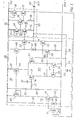
- Referring now to the drawings, wherein like reference numerals designate identical or corresponding parts throughout the several views, and more particularly to Figure 1 thereof, in this embodiment, transistors (52) and (53) are output transistors being protected by a protection circuit (10) according to this invention.
- In this configuration, the output transistors (52) and (53) are arranged and operated as a complementary class B push-pull amplifier (30). In a class B push-pull amplifier, one of the output transistors is operative only for positive going portions of output signal and the other is operative only for negative going portions of the output signals, and the overall operation is quasi-linear.
- The amplifier (30) includes a differential amplifier (60). The input signal thereto is supplied to the base electrode of the transistor (31), namely input terminal (IN). The output signal of this amplifier (60) is supplied to the base electrode of the transistor (49). The collector electrode of,transistor (49) is connected to the base electrode of output transistor (52) through diodes (47), (48), and directly to the base electrode of transistor (53). These diodes (47) and (48) provide a potential offset between base electrodes of transistors (52) and (53), which offset potential minimizes cross-over distortion of the amplifier.
- Output transistors (52) and (53) are respectively operative only for positive going portions or negative going portions of the output signal of transistor (49). Output signals from the emitter electrodes of transistors (52) and (53) are combined at the output line (55), and delivered from output terminal (Out) through the coupling capacitor (54).
- A constant current source (70) for this amplifier is constructed by resistor (38), diodes (39) (40), transistor (41) and resistor (42). A constant current from the current source (70) is supplied to the differential amplifier (60) and output transistors (52) and (53) by current mirror. configuration (80) comprising transistors (43) (44) and (46).
- Additionally, the amplifier (30) includes a negative feedback circuit including resistors (54), (55) and capacitor (56). The one end of the resistor (54) is connected to the output line (55) and the other end is connected to the base electrode of transistor (32).
- The protection circuit (10) according to this invention includes a transistor (11) having a base electrode connected to the base electrode of transistor (52), an emitter electrode connected to the output line (55) through the resistor (12), and a collector electrode connected to terminal A and to the power supply terminal (Vcc) through the diode configuration transistor (14) and the resistor (13). The protection circuit (10) further includes a transistor (15) having a base electrode connected to the terminal (A), a collector electrode connected to the power supply terminal (Vcc), and an emitter electrode connected to the output line (55) through a resistor(16). Further included is a transistor (17) having a base electrode connected to the emitter electrode of the transistor (15), and an emitter electrode connected to the power supply terminal (Vcc) through a diode configuration transistor (18), and a collector electrode connected to the base electrode of transistor (19), and this collector electrode supplies the protecting signal.
- Now the operation and the principle of the protection circuit (10) will be explained.
- The base to emitter voltage VBE52 of the transistor (52) can be expressed as

- q : charge on an electron
- k : Boltzman's constant
- T : Operating temperature in degrees in Kelvin
- IC52 : Collector current of transistor (52)
- IS52 : Saturation current of transistor (52)
- Ae52 : Emitter area of transistor (52)
- VBE52 is equal to the sum of the base to emitter voltage VBE11 of the transistor (11) and the voltage drop VR12 of the resistor (14). So,

- Assuming the values of the resistors (12) and (13) are equal, the voltage VBE52 is also equal to the voltage between the power supply terminal (Vcc) and terminal (A).
- So the equation (2) can be expressed as


- VCE52 : collector to emitter voltage of transistor (52)
- VF : base to emitter voltage of transistors (17) and (18)
- R16 : resistance value of resistor (16)
- The voltage VB between the power supply terminal (Vcc) and the terminal (B) is the sum of the voltage VA between the power supply terminal (Vcc) and the terminal (A) and the base to emitter voltage VBE15 of transistor (15), and the voltage VA is equal to the VBE52, so


- On the other hand, VB is the sum of the base to emitter voltage VBE17 of the transistors (17) and (18).
- Namely, .

- Assuming the collector currents IC17 and IC18 are eqial, the equation (8) can be rewritten as


- It is apparent from equation (11), the collector current IC17 of transistor (17) is proportional to the product of the collector current IC52 and the collector to emitter voltage VCE52, namely the power consumption of output transistor (52).
- So protecting the output transistor (52) in accordance with the level of the collector current I of transistor (17) effectively protects the output transistor (52) in accordance with its power consumption.
- The collector electrode of transistor (17) is connected to the base electrode of transistor (19). The emitter electrode of transistor (19) is grounded, and collector electrode is connected to the base electrode of transistor (41). A resistor (20). is.connected between the base electrode of transistor (19) and ground terminal (Gnd).
- The protection operation starts when transistor (19) becomes conductive, so that the transistor (41) tends to turn off. When the transistor (41) is turned off, the constant current supply to differential amplifier (60) and output transistor (52) and (53) is cut off, thus protecting the output transistors.
- To vary the protection operation start level, the resistance value of resistors (12), (13), (16) and (20), and the emitter areas of the transistors forming the protection circuit (10) may be varied.
- This means, for example, that it is not'necessary to match the voltages VBE52 and VA. The important thing is to develop the voltage dependent upon the collector current of output transistor (52) between the terminal (A) and power supply terminal (Vcc).
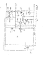
- Figure 2 shows another embodiment of this invention.
- In this configuration, the protection circuit (10) according to this invention is adapted to protect the output transistor (53). Thus in this configuration the protection operation is performed at the negative going portions of the input signal.
- The detecting signal, namely the collector current IC17 I I of transistor (107) is expressed as


- VF : base to emitter voltage of transistors (107) and (108).
- The collector current (107) may be supplied to the same terminal, namely to base electrode of the transistor (19) being inverted using current mirror circuit (40).
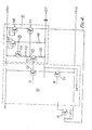
- Fig. 3 shows another embodiment of this invention this invention.
- In this configuration, diode (14') and (18') are shown instead of the diode configuration transistors (14) and (18) in Fig. 1. Also constant current source (31) is further added. Namely, the constant current source (31) includes transistors (33), (35), diode (34) and resistor (36). The collector electrode of transistor (35) is connected to the emitter electrode of transistor (17). This constant current source (31) serves to vary the protection level for the protection operation.
- Fig. 4 shows another preferred embodiment according to this invention. In this configuration, the protection circuit (10) includes transistors (111), (114), (117), diodes (115), (118) and resistors (112), (113), (116). Of course, instead of diodes.(115), (117), diode configuration transistors may be used.
- In this configuration, base to emitter voltage VBE52 is equal to the sum of the base to emitter voltage VBE111 of transistor (111) and the voltage drop VR112 of resistor (112). So,

- Assuming that the collector currents IC111 and IC114 of transistors (111) and (114) are equal, and resistance value R112, R113 of resistors (112), (113) are equal, the voltage between the terminals C and D is also equal to VBE52.

- The current flowing in resistor (116) can be expressed as

- Assuming this I116 is equal to the collector current of transistor (115), the base to emitter voltage VBE115 of transistor (115) can.be expressed as

- So the voltage Vc between the (Vcc) terminal and terminal (C) can be expressed as the sum of the base to emitter voltage VBE52 of transistor (52) and V BE115 of transistor (115) expressed by equations (1) and (16) respectively. So

- This voltage VC is equal to the sum voltage of VBE117 and VBE118 of transistors (117) and (118). So

- Assuming collector currents IC117 and IC118 of transistors (117) and (118) are equal, the following equation is obtained by combining equations (17) and (18):
-


- It is apparent from equation (19), the collector current IC117 of transistor (117) is also a function of the product of the collector current IC52 and the collector to emitter voltage VCE52 of transistor (52), so it is possible to detect the power consumption of transistor (52) by detecting the collector current IC117 of transistor (117). This collector current IC117 is supplied to the base electrode of the transistor (19). The protection operation is the same, as previously explained in the embodiment shown in Fig. 1 to Fig. 3.
- As previously explained, in accordance with this invention the protection operation is performed by monitoring the power consumption of the output transistor, as determined by the variation of collector current and collector to emitter voltage of the output transistor. Therefore, the protection circuit can operate over the entire A.S.O. (Area of Safety Operation) of the transistor.
- The protection circuit according to this invention may be adapted to protect many other types of output circuit, and the protecting signal from the protection circuit may be used for indicating the excess power consumption of the output transistors.
- Obviously, numerous additional modifications and variations of the present invention are possible in light of the above teachings. It is therefore to be understood that within the scope of the appended claims, the invention may be practiced otherwise than as specifically described herein.
Claims (11)
Applications Claiming Priority (2)
| Application Number | Priority Date | Filing Date | Title |
|---|---|---|---|
| JP10569/81 | 1981-01-27 | ||
| JP56010569A JPS57124909A (en) | 1981-01-27 | 1981-01-27 | Output transistor protection circuit |
Publications (2)
| Publication Number | Publication Date |
|---|---|
| EP0058005A1 true EP0058005A1 (en) | 1982-08-18 |
| EP0058005B1 EP0058005B1 (en) | 1985-08-14 |
Family
ID=11753867
Family Applications (1)
| Application Number | Title | Priority Date | Filing Date |
|---|---|---|---|
| EP82300362A Expired EP0058005B1 (en) | 1981-01-27 | 1982-01-25 | Protection circuit for an output transistor |
Country Status (4)
| Country | Link |
|---|---|
| US (1) | US4538198A (en) |
| EP (1) | EP0058005B1 (en) |
| JP (1) | JPS57124909A (en) |
| DE (1) | DE3265316D1 (en) |
Cited By (3)
| Publication number | Priority date | Publication date | Assignee | Title |
|---|---|---|---|---|
| EP0280327A2 (en) * | 1987-02-27 | 1988-08-31 | Kabushiki Kaisha Toshiba | Audio output amplifier |
| EP0570617A1 (en) * | 1992-05-19 | 1993-11-24 | Pioneer Electronic Corporation | Protective apparatus for power transistor |
| EP0772273A1 (en) * | 1995-10-31 | 1997-05-07 | STMicroelectronics S.r.l. | Sensor of the instant power dissipated in a power transistor |
Families Citing this family (8)
| Publication number | Priority date | Publication date | Assignee | Title |
|---|---|---|---|---|
| US4651252A (en) * | 1985-03-29 | 1987-03-17 | Eaton Corporation | Transistor fault tolerance method and apparatus |
| US4730122A (en) * | 1986-09-18 | 1988-03-08 | International Business Machines Corporation | Power supply adapter systems |
| JPH0630543B2 (en) * | 1987-01-13 | 1994-04-20 | 株式会社東芝 | Output circuit abnormality detection notification circuit |
| US4949213A (en) * | 1988-11-16 | 1990-08-14 | Fuji Electric Co., Ltd. | Drive circuit for use with voltage-drive semiconductor device |
| DE19527487C1 (en) * | 1995-07-27 | 1997-02-27 | Texas Instruments Deutschland | Circuit arrangement for testing functioning of current monitor circuit for power transistor |
| US5896263A (en) * | 1997-06-27 | 1999-04-20 | Allen-Bradley Company, Llc | Output circuit having electronic overload protection activated by voltage drop across output transistor |
| US6330143B1 (en) | 2000-02-23 | 2001-12-11 | Ford Global Technologies, Inc. | Automatic over-current protection of transistors |
| US6448855B1 (en) * | 2000-04-13 | 2002-09-10 | Koninklijke Philips Electronics N.V. | Accurate power detection circuit for use in a power amplifier |
Citations (5)
| Publication number | Priority date | Publication date | Assignee | Title |
|---|---|---|---|---|
| DE2154720B2 (en) * | 1971-02-01 | 1975-07-10 | Zentrallaboratorium Fuer Rundfunk- Und Fernsehempfangstechnik, X 8060 Dresden | Protective voltage monitor - has transistor in series and transistor across load triggering alarm when volts fall or rise |
| GB1439241A (en) * | 1972-07-27 | 1976-06-16 | Sony Corp | Transistor amplifiers including a protective circuit |
| US4021701A (en) * | 1975-12-08 | 1977-05-03 | Motorola, Inc. | Transistor protection circuit |
| DE2705583A1 (en) * | 1977-02-10 | 1978-08-17 | Siemens Ag | Power transistor circuit with protection against overheating - makes comparison of base-emitter voltage with reference to trigger safety system |
| DE3003123A1 (en) * | 1979-01-29 | 1980-08-07 | Rca Corp | OVERCURRENT PROTECTION SWITCH FOR A POWER TRANSISTOR |
Family Cites Families (1)
| Publication number | Priority date | Publication date | Assignee | Title |
|---|---|---|---|---|
| US4355341A (en) * | 1980-06-30 | 1982-10-19 | Rca Corporation | Power protection circuit for transistors |
-
1981
- 1981-01-27 JP JP56010569A patent/JPS57124909A/en active Granted
-
1982
- 1982-01-25 EP EP82300362A patent/EP0058005B1/en not_active Expired
- 1982-01-25 DE DE8282300362T patent/DE3265316D1/en not_active Expired
-
1984
- 1984-07-21 US US06/515,680 patent/US4538198A/en not_active Expired - Lifetime
Patent Citations (6)
| Publication number | Priority date | Publication date | Assignee | Title |
|---|---|---|---|---|
| DE2154720B2 (en) * | 1971-02-01 | 1975-07-10 | Zentrallaboratorium Fuer Rundfunk- Und Fernsehempfangstechnik, X 8060 Dresden | Protective voltage monitor - has transistor in series and transistor across load triggering alarm when volts fall or rise |
| GB1439241A (en) * | 1972-07-27 | 1976-06-16 | Sony Corp | Transistor amplifiers including a protective circuit |
| US4021701A (en) * | 1975-12-08 | 1977-05-03 | Motorola, Inc. | Transistor protection circuit |
| DE2705583A1 (en) * | 1977-02-10 | 1978-08-17 | Siemens Ag | Power transistor circuit with protection against overheating - makes comparison of base-emitter voltage with reference to trigger safety system |
| DE3003123A1 (en) * | 1979-01-29 | 1980-08-07 | Rca Corp | OVERCURRENT PROTECTION SWITCH FOR A POWER TRANSISTOR |
| GB2042297A (en) * | 1979-01-29 | 1980-09-17 | Rca Corp | Overcurrent protection circuit for power transistor |
Cited By (5)
| Publication number | Priority date | Publication date | Assignee | Title |
|---|---|---|---|---|
| EP0280327A2 (en) * | 1987-02-27 | 1988-08-31 | Kabushiki Kaisha Toshiba | Audio output amplifier |
| EP0280327A3 (en) * | 1987-02-27 | 1989-04-26 | Kabushiki Kaisha Toshiba | Audio output amplifier |
| EP0570617A1 (en) * | 1992-05-19 | 1993-11-24 | Pioneer Electronic Corporation | Protective apparatus for power transistor |
| US5383083A (en) * | 1992-05-19 | 1995-01-17 | Pioneer Electronic Corporation | Protective apparatus for power transistor |
| EP0772273A1 (en) * | 1995-10-31 | 1997-05-07 | STMicroelectronics S.r.l. | Sensor of the instant power dissipated in a power transistor |
Also Published As
| Publication number | Publication date |
|---|---|
| JPS57124909A (en) | 1982-08-04 |
| JPS6255725B2 (en) | 1987-11-20 |
| US4538198A (en) | 1985-08-27 |
| DE3265316D1 (en) | 1985-09-19 |
| EP0058005B1 (en) | 1985-08-14 |
Similar Documents
| Publication | Publication Date | Title |
|---|---|---|
| US3449680A (en) | Transistor protection circuit | |
| JPH0683042B2 (en) | Output driver circuit | |
| EP0058005A1 (en) | Protection circuit for an output transistor | |
| US4453092A (en) | Comparator circuit having reduced input bias current | |
| US5006949A (en) | Temperature compensated overload trip level solid state relay | |
| JPH0661432A (en) | Semiconductor device | |
| US4884161A (en) | Integrated circuit voltage regulator with transient protection | |
| WO1993017492A1 (en) | Current detecting circuit | |
| US3931547A (en) | Protection circuit | |
| JPH0630543B2 (en) | Output circuit abnormality detection notification circuit | |
| US3924159A (en) | Amplifier protection system | |
| JPS59144208A (en) | Apparatus for protecting power element of integrated circuit | |
| EP0132863A1 (en) | Protection circuit | |
| EP0802604A3 (en) | Protection circuit | |
| US4225797A (en) | Pulse generator circuit triggerable by nuclear radiation | |
| JPH02117211A (en) | Semiconductor device | |
| WO1998021820A1 (en) | Arrangement for protecting the output transistors in a power amplifier | |
| KR900007032B1 (en) | Over load protecting circuit of push pull amp output | |
| US3947696A (en) | Touch actuated electronic switch | |
| JPH11160370A (en) | Abnormal voltage detection circuit | |
| SU1453390A1 (en) | Stabilized power supply source | |
| US5006791A (en) | Electrostatic detector and method for detecting conductors | |
| JP2515332B2 (en) | Circuit arrangement for protecting the push-pull output stage from overload | |
| JPS59210704A (en) | Semiconductor integrated circuit device | |
| JPS61117613A (en) | Constant voltage power supply circuit with current limit |
Legal Events
| Date | Code | Title | Description |
|---|---|---|---|
| PUAI | Public reference made under article 153(3) epc to a published international application that has entered the european phase |
Free format text: ORIGINAL CODE: 0009012 |
|
| AK | Designated contracting states |
Designated state(s): DE GB IT |
|
| 17P | Request for examination filed |
Effective date: 19830128 |
|
| RAP1 | Party data changed (applicant data changed or rights of an application transferred) |
Owner name: KABUSHIKI KAISHA TOSHIBA |
|
| ITF | It: translation for a ep patent filed |
Owner name: STUDIO CONS. BREVETTUALE S.R.L. |
|
| GRAA | (expected) grant |
Free format text: ORIGINAL CODE: 0009210 |
|
| AK | Designated contracting states |
Designated state(s): DE GB IT |
|
| REF | Corresponds to: |
Ref document number: 3265316 Country of ref document: DE Date of ref document: 19850919 |
|
| PLBE | No opposition filed within time limit |
Free format text: ORIGINAL CODE: 0009261 |
|
| STAA | Information on the status of an ep patent application or granted ep patent |
Free format text: STATUS: NO OPPOSITION FILED WITHIN TIME LIMIT |
|
| 26N | No opposition filed | ||
| REG | Reference to a national code |
Ref country code: GB Ref legal event code: 746 |
|
| ITTA | It: last paid annual fee | ||
| PGFP | Annual fee paid to national office [announced via postgrant information from national office to epo] |
Ref country code: GB Payment date: 19980116 Year of fee payment: 17 |
|
| PGFP | Annual fee paid to national office [announced via postgrant information from national office to epo] |
Ref country code: DE Payment date: 19980202 Year of fee payment: 17 |
|
| PG25 | Lapsed in a contracting state [announced via postgrant information from national office to epo] |
Ref country code: GB Free format text: LAPSE BECAUSE OF NON-PAYMENT OF DUE FEES Effective date: 19990125 |
|
| GBPC | Gb: european patent ceased through non-payment of renewal fee |
Effective date: 19990125 |
|
| PG25 | Lapsed in a contracting state [announced via postgrant information from national office to epo] |
Ref country code: DE Free format text: LAPSE BECAUSE OF NON-PAYMENT OF DUE FEES Effective date: 19991103 |