EP0057788A2 - Data processing system with external microcode control unit - Google Patents
Data processing system with external microcode control unit Download PDFInfo
- Publication number
- EP0057788A2 EP0057788A2 EP81305587A EP81305587A EP0057788A2 EP 0057788 A2 EP0057788 A2 EP 0057788A2 EP 81305587 A EP81305587 A EP 81305587A EP 81305587 A EP81305587 A EP 81305587A EP 0057788 A2 EP0057788 A2 EP 0057788A2
- Authority
- EP
- European Patent Office
- Prior art keywords
- microinstructions
- unit
- microinstruction
- macroinstruction
- external
- Prior art date
- Legal status (The legal status is an assumption and is not a legal conclusion. Google has not performed a legal analysis and makes no representation as to the accuracy of the status listed.)
- Granted
Links
Images


Classifications
-
- G—PHYSICS
- G06—COMPUTING; CALCULATING OR COUNTING
- G06F—ELECTRIC DIGITAL DATA PROCESSING
- G06F9/00—Arrangements for program control, e.g. control units
- G06F9/06—Arrangements for program control, e.g. control units using stored programs, i.e. using an internal store of processing equipment to receive or retain programs
- G06F9/30—Arrangements for executing machine instructions, e.g. instruction decode
- G06F9/30145—Instruction analysis, e.g. decoding, instruction word fields
-
- G—PHYSICS
- G06—COMPUTING; CALCULATING OR COUNTING
- G06F—ELECTRIC DIGITAL DATA PROCESSING
- G06F9/00—Arrangements for program control, e.g. control units
- G06F9/06—Arrangements for program control, e.g. control units using stored programs, i.e. using an internal store of processing equipment to receive or retain programs
- G06F9/22—Microcontrol or microprogram arrangements
- G06F9/26—Address formation of the next micro-instruction ; Microprogram storage or retrieval arrangements
- G06F9/262—Arrangements for next microinstruction selection
- G06F9/268—Microinstruction selection not based on processing results, e.g. interrupt, patch, first cycle store, diagnostic programs
-
- G—PHYSICS
- G06—COMPUTING; CALCULATING OR COUNTING
- G06F—ELECTRIC DIGITAL DATA PROCESSING
- G06F9/00—Arrangements for program control, e.g. control units
- G06F9/06—Arrangements for program control, e.g. control units using stored programs, i.e. using an internal store of processing equipment to receive or retain programs
- G06F9/22—Microcontrol or microprogram arrangements
- G06F9/28—Enhancement of operational speed, e.g. by using several microcontrol devices operating in parallel
-
- G—PHYSICS
- G06—COMPUTING; CALCULATING OR COUNTING
- G06F—ELECTRIC DIGITAL DATA PROCESSING
- G06F9/00—Arrangements for program control, e.g. control units
- G06F9/06—Arrangements for program control, e.g. control units using stored programs, i.e. using an internal store of processing equipment to receive or retain programs
- G06F9/30—Arrangements for executing machine instructions, e.g. instruction decode
- G06F9/38—Concurrent instruction execution, e.g. pipeline, look ahead
- G06F9/3818—Decoding for concurrent execution
- G06F9/3822—Parallel decoding, e.g. parallel decode units
Definitions
- This invention relates to data processing systems using microprocessors and, more particularly, to systems which use microcode architecture and are capable of responding to externally supplied microcoded instructions by utilizing unique interface techniques therefor.
- Data processing systems have generally been developed to provide system configurations which range from compact single-board micro-computers to more complex high performance mini-computers.
- Such systems use microcode architecture in which macroinstructions are suitably decoded so as to provide access to a micro-instruction or to a sequence of more than one micro-instruction obtained from a suitable data store thereof.
- the microcontrol store is formed as an "orthogonal" store in which a first, or “vertical”, microcontrol store provides a "narrow" microinstruction word portion having one field comprising a selected number of vertical microinstruction bits for selecting one of a plurality of second, or “horizontal”, microinstructions from a second level, or horizontal, microcontrol store, one or more "modifier” fields, as described in such application, and a sequencing field for presenting the address of the next (i.e. each successive) vertical microinstruction in a sequence thereof.
- microinstructions can be fetched either from a CPU-resident vertical control ROM or from one or more external microcontrollers via one or more external microcontroller interface units.
- the external microcodes can be obtained at any one time from one of the plurality of external microcontroller units by the use of suitable time-multiplexing techniques using a time-multiplexed microcode bus.
- the CPU requires appropriate logic which responds to software for identifying the macroinstruction to be decoded as one which requires decoding either by the internal microcode architecture or by the external microcode architecture. Once the CPU has identified the macroinstruction as requiring an external microcode decoding procedure, it supplies the macroinstruction to the designated external microcontroller unit which then proceeds to decode the macroinstruction so as to provide the initial micro- instruction via the microcode bus.
- the CPU then utilizes its own internal sequencing logic and microcode control store to provide the subsequent microinstructions of the particular sequence required by the decoded macroinstruction. Control of the macroinstruction decoding process, as well as the process for determining the address of each subsequent microinstruction required in the sequence, effectively, therefore, resides in the CPU.
- the present invention is defined in claim 1 below and provides a more effective way for providing the external microcode information. While the invention is applicable to multi-level microcode systems, its use is not limited thereto and the principles thereof are also applicable to single-level systems.
- every macroinstruction supplied, for example, by software to the system is simultaneously initially decoded by both the CPU-resident microcode control unit and the microcode interface units.
- a subset of the operational code (OP-CODE) in the macroinstruction identifies which type of microcode control unit (i.e. an external microcode unit or an internal, i.e. a CPU-resident, unit) is required to perform the decoding operation in order to produce the required microinstruction or sequence of microinstructions.
- an appropriate acknowledge signal is provided by the selected external unit so that the external microcode controller can override the CPU-resident controller and, therefore, can provide the required decoding operation.
- the external microcontrol interface unit includes logical capability for determining the successive addresses of successive microinstructions in a sequence thereof within the external interface unit itself without the need for any logical operations to be performed by any CPU-resident control logic units.
- the external microcontrol interface unit also has logic for monitoring the transfer of microinstructions from the external unit to the CPU and for monitoring the execution thereof by the CPU so that, at any point in time, the external microcontroller unit keeps track of the difference between how many microinstructions have been transferred and how many of these microinstructions have been executed by the CPU, and, accordingly, how many of the transferred microinstructions have yet to be executed.
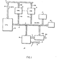
- the system which is shown in Fig 1 has a microprocessor unit, identified as a central processor unit or CPU 10, interconnected via an appropriate system bus 11 with a memory system 12, one or more system input/output (I/O) units 17, I/O interface units 14 and 14A for interfacing I/O units via different I/O bus means 15 and 15A, respectively, and one or more external microcontroller (XMC) interface units 13.
- the system bus 11 may be in the form of a 16-bit parallel system bus while 16-bit microcode inputs from an external microcontroller unit 13 can be transmitted to the CPU in a time-multiplexed fashion via an intermediate 8-bit bus 13A and an 8-bit microcode bus 16. Further 16-bit intermediate system buses 11A are provided from the main system bus 11 to the external microcontroller units 13 as shown.
- Fig 1 The system of Fig 1 is generally as described in the aforementioned EP 0035334 and the particular operation of the CPU and its operational relationship with the memory and various I/O units and buses is described therein in detail. Further explanation of such detailed operation is not necessary in order to describe this invention and, accordingly, reference is made to the published application for an understanding of the overall system operation. For convenience, the present invention is described as used in such a multi-level microcode system although, as mentioned above, its use is not limited thereto.
- the external microcontrol interface unit of the invention permits control of the macroinstruction decoding and the sequencing of the microinstructions to reside fully in the external microcontroller unit itself so as to provide a more effective and efficient use of an instruction register "pipe-lining" process which is conventionally utilized in the CPU of such a two-level microcode system of the type described above.
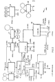
- FIG. 2 shows an exemplary external microcontroller interface (XMC) unit 13 having a configuration which would be utilized in each of the XMC units 13 shown in FIG. 1.
- XMC external microcontroller interface
- FIG. 2 shows an exemplary external microcontroller interface (XMC) unit 13 having a configuration which would be utilized in each of the XMC units 13 shown in FIG. 1.
- a macroinstruction is supplied under control of CPU via an intermediate system bus 11A, such macroinstruction being defined by a suitable 16-bit word, as shown.
- the macroinstruction is supplied to the XMC instruction register 20 which supplies such macroinstruction, in a pipe-lined manner, to a decode/matrix unit 21 which utilizes a suitable instruction program logic array (IPLA) matrix providing for appropriate decoding of the macroinstruction to produce an initial microinstruction.
- IPLA instruction program logic array
- the initial microinstruction includes the horizontal address bits field (ADRH) and the two vertical modifier fields (V 1 , V 2 ), the six-bit horizontal address and each of the four-bit vertical modifiers being supplied to the CPU via the XMC bus 16 and intermediate bus 13A through an appropriate multiplexer and buffer unit 22.
- the multi plexer unit supplies such fields as part of two time-multiplexed eight-bit bytes as depicted at the output thereof.
- the I P L A decode unit 21 also supplies a two-bit "initial next address mode" (INAM) signal via a next address ROM unit 23 to the multiplexer buffer unit 22 so that a total of 16-bits (ADRH, Vl, V2 and INAM) are supplied via multiplexer and buffer unit 22 to bus 13A for the initial microinstruction.
- INAM "initial next address mode”
- the IPLA decode/matrix unit 21 also supplies a next address mode (NEXT) field of 10 bits and an initial address control (IADRC) field of 10 bits to the XMC sequence logic unit 24, the structure and operation of which is explained in more detail with reference to FIG. 3.
- NXT next address mode
- IADRC initial address control
- the sequence unit 24 then controls the supplying of a sequence of horizontal address and vertical modifier fields via a control program logic array decode (CPLA) matrix unit. 25, as discussed below, each of the sequence of horizontal addresses and vertical modifiers then being appropriately supplied in sequence via multiplexer/buffer unit 22 to the CPU, following the prior supplying thereto of the initial address and modifiers directly from the IPLA decode/matrix unit 21.
- CPLA control program logic array decode
- the next address can be supplied to sequence logic 24 from a source external to the microcontroller unit 13 via a dispatch register 26, such addresses being dispatched to the external microcontroller unit 13 via system bus 11 and interconnecting XMC bus 11A under the control of appropriate dispatch control logic 27.
- Suitable timing logic unit 28 is utilized to provide suitable timing control signals to the various components of the external microcontrol unit 13.
- FIG. 3 depicts in more detail the elements of the external microcontroller (XMC) sequence logic unit 24.
- an appropriate multiplexer 30 supplies an address input to a program counter 31, such input being selected from either the IPLA decode unit 21 (the IADRC field), the CPLA matrix unit 25 (the ADRC field), or the dispatch register 26 (the DREG field). Alternatively, such address can be supplied to program counter 31 as a feedback input from a last in/ first out memory stack 32.
- An appropriate control signal ADEC for the multiplexer unit is supplied from an IPLA control logic unit 29 (see FIG. 2).
- each macroinstruction When a request to decode a macroinstruction is issued by the CPU of FIG. 1, each macroinstruction includes within it the information which determines whether such macroinstruction is to be decoded by the internal, i.e., the CPU-resident, decoding units of the processor 10 or by an external micro- controller unit 13.
- each macroinstruction is arranged so that it has a unique bit pattern which can only be decoded by either the internal decoding units of the processor or the decoding units of a specified external microcontroller interface unit. In certain cases where a particular external microcontroller unit, such as shown in FIGS.
- the IPLA decode/matrix unit 21 indicates such recognition by asserting a single bit MYINS ("my instruction") which is supplied to the IPLA control logic 29 to cause the assertion of an ACK ("acknowledge”) signal for supply to the processor.
- MYINS my instruction
- ACK acknowledgenowledge
- an acknowledge (ACK) signal from the microcontroller interface unit is always interpreted by the central processor unit as requiring external microcode decoding, even if the CPU resident processor decoding units could decode such macroinstruction. Accordingly, decoding by the external unit prevails. Such operation is designated as an "external microcode override" condition. If no ACK signal is asserted from any external microcontroller unit, the processor utilizes its own internal macrocode decoding units, as discussed in the aforementioned application for performing the macroinstruction decoding operation.
- the assertion of a MYINS signal together with the assertion of an appropriate "tri-state enable” (TSE) signal, will produce a "tri-state” (TS) signal from the IPLA control logic 29 for controlling the operation of the multiplexer/buffer register 22,
- TSE tri-state enable
- TS tri-state signal from the IPLA control logic 29 for controlling the operation of the multiplexer/buffer register 22
- the TS signal is not asserted unless the MYINS signal has been asserted by the IPLA decode/matrix unit 21 to indicate that the particular microcontroller unit 13 in question has been selected for the decoding operation.
- the XMC bus 16 can be driven only by one external microcontroller : unit at a time so that bus burn-out problems that may occur ifmultiple external units are attempting to drive the bus simultaneously are avoided.
- the IPLA control logic 29 provides an appropriate decode control signal (A D EC) which in effect represents a basic initiation signal for operation of the external microcontroller unit so as to permit appropriate decoding of the incoming macroinstruction to proceed.
- a D EC decode control signal
- the macroinstruction is initially decoded by the IPLA decode/matrix unit 21 which receives 32 bits comprising the 16 bit macroinstruction word and the 16 inversion bits therefor via the instruction register pipe line system 20, such system for handling incoming information in a pipe-lined fashion being well known to the art.
- the decoded macro nstruction word selects the correct initial microinstruction word at the decoded address from the IPLA storage matrix which comprises a plurality of stored microinstruction words.
- the initial microinstruction word from the IPLA matrix comprises the following fields as shown below. As can be seen, the microinstruction word is 38 bits.wide and includes 8 fields.
- the ADRH, V1, and V2 fields are effectively the same as those described in the aforesaid application with reference to the horizontal address and vertical modifier fields of the initial microinstruction decoded by the CPU-resident decoding units. Such fields are appropriately supplied to the horizontal decoder and to the vertical modifier unit, respectively, in the manner discussed in the previously filed application.
- the MYINS bit has been discussed above.
- the DEC field merely indicates which operation mode will be used with respect to the next address in the microinstruction sequence.
- the DEC bit signifies either that the next operating mode will require a decoding of the next micro- . instruction of a sequence thereof or will require a call for a new macroinstruction (e.g., if there is only a single micro- instruction in the current sequence).
- the DEC bit and the four CNAM bits from the CNAM ROM 38 (FIG. 3) generate the NAM bits via next address logic unit 23, which are transmitted to the CPU with the ADRH, VI and V2 fields to indicate to the CPU the four operations discussed below.
- the IADRC field provides the address of one of the microinstructions (e.g., one of 1024 microinstructions in an exemplary embodiment) which are stored in the CPLA matrix unit 25.
- the selected microinstruction may either be executed next following the execution of the current micro- instruction, or not, depending on the interpretation of the next address mode (NAM) field or the next address mode extensions (CNAMX) field, as discussed below.
- NAM next address mode
- CNAMX next address mode extensions
- the CNAMX field sets a plurality of appropriate flags (FLAG A, FLAG B or FLAG C) to their initial state in accordance with the following table:
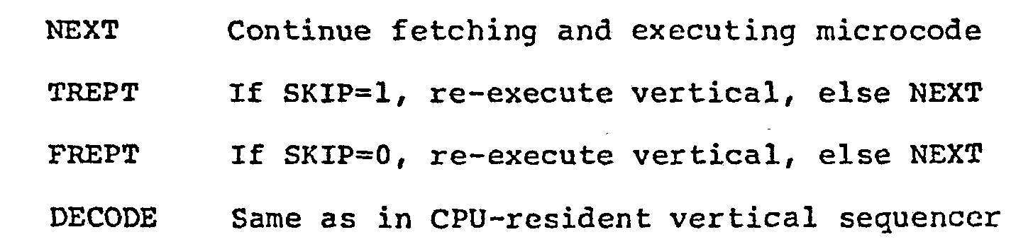
- the next address mode (NAM) field indicates whether the external microcontroller sequencing operation should continue with the fetching and execution of the next microinstruction of the sequence or whether it should continue to re-execute the same vertical modifiers in the currently executing microinstruction in accordance with whether the NAM field indicates a true repeat (TREPT) or a false repeat (FREPT) condition.
- the NAM field further determines whether or not a decode operation should take place as discussed with reference to the vertical sequence unit of the processor as discussed in the aforesaid application.
- the NAM field conditions are summarized as follows:
- the NEXT field points to an address of one of the microinstructions in the CPLA.
- Such pointer provides the value of the control program counter subsequent to the current program counter content (i.e., CPC+1 in FIG. 3) which is needed by the CNAM micro-order CALL.
- the CPC+1 is not otherwise available without the NEXT field since the IPLA decode/matrix unit 21 is not addressed by the control program counter (instead it is the IPLA which initializes the control program counter).
- the NEXT field in effect pushes a return to the stack (FIG. 3) so that the system knows where to return after a sub-routine has been executed.
- the next microinstruction, and each subsequent one of a sequence thereof is supplied by the CPLA matrix unit 25 which selects a microinstruction at the selected address therein.
- the microinstruction that is selected supplies the ADRH, Vl and V2 fields to the output multiplexer/buffer unit 22 and, thence, to the external microcode bus 16.
- the complete field representation for a microinstruction obtained from the CPLA matrix unit 25 is shown below:
- the ADRH, V1 and V2 fields of the 31 bit CPLA micro- instruction word are as discussed above with reference to the IPLA microinstruction word and supply the horizontal address land vertical modifier fields to the processor via microcode bus 16.
- the ADRC field provides the address of one of the microinstructions in the CP LA matrix unit 25. Such microinstruction'may or may not be executed next depending on the interpretation of the CNAM and CNAMX fields, the ADRC field specifying both unconditional and conditional branch addresses which are to be used in determining the new control program counter (PC) value.
- PC new control program counter
- the CNAM field is a four bit field which specifies one of the following 14 encodings.
- the first 7 encodings are unconditionals while the rest are conditionals, which conditions are specified by the CNAMX field disrussed below.
- the subroutine stack (shown in FIG. 3) is four deep (stacks ⁇ -3) so that only four nested subroutine calls are possible.
- the DRE G refers to the dispatch register 26 shown in FIG. 2.
- the CNAMX field has 8 encodings for both unconditionals and conditionals as follows:
- waiting (Wait ⁇ -Wait 3) is necessary due to the delay between the XMC microinstruction fetch by the XMC, the XMC microninstructicn fetch by the CPU, the target horizontal's execution by the CPU, and the receipt of SKIP by the XMC unit, or the external loading of the dispatch register 26. Waiting is not necessary when any flag is specified because the flags are implemented by the XMC unit and are immediately available.
- the HTBEC (horizontals-to-be-executed) counter 37 indicates how many microinstructions have been sent to the CPU but have not yet been executed.
- the HTBEC counter is incremented by the ACK signal, is decremented by the H OR E X signal and is cleared by the ADEC signal.
- the contents thereof are compared to the WAIT request signal from the CNAMX ROM 35 in the flags/condition logic 36 to assure that the SKIP signal is returned for the microinstruction of interest (as discussed in more detail below with respect to the timing diagram of FIG. 4).
- the flags/ condition logic 36 asserts a HOLD signal to hold the operation of the program counter 31 until the above-mentioned comparison indicates that the appropriate SKIP signal has been received.
- the HOREX signal for the particular microinstruction of interest is received in phase II of a cycle
- the SKIP signal for that microinstruction is returned in phase I of the following cycle.
- FIG. 4 depicts various key signals which are asserted during the exemplary operation (and shown on FIGS. 2 and 3) while Chart I depicts the sequence of steps performed in the exemplary operations.
- Each of the CLOCK cycles has two phases (I and II), a sequence of 15 cycles being shown in the example depicted.
- the CPU requests a macrocode decode operation M by asserting a MACR signal (a "macrocode” request) during phase II of cycle 1, immediately followed by a MICR signal (a "microcode” request) during phase I of cycle 2.
- a macrocode is one which can be handled by the particular external microcontroller unit
- such unit decodes the macroinstruction and asserts its ACK signal to show performance of the decode operation so as to produce the initial microinstruction A at the XMC bus.
- such microinstruction is placed on the bus in two portions Al and A2 shown at the C bus at phase II of cycle 2 and at phase I of cycle 3, while acknowledging the decoding thereof, as mentioned above, by asserting the ACK signal at phase II of cycle 2.
- such microinstruction is a test instruction and is fetched from the IPLA decode/matrix unit 21. If the DEC field does not indicate that the decoding of a new macroinstruction is required (as, for example, when the currently decoded macroinstruction contained only a single micro- instruction), the next microinstruction B is fetched from the CPLA matrix unit 25. Microinstruction A 1 , A 2 is sent on the XMC bus to the CPU for execution while the HTBEC counter is incremented by "1" to show that a microinstruction has been sent to the CPU for execution but has not yet been executed.
- next microinstruction C is then fetched from the CPLA and transmitted to the CPU. While this operation would normally increment the HTBEC to "3", by this time the first microinstruction A has been executed and the assertion of the HOREX (horizontal executed) signal from the CPU simultaneously decrements the HTBEC by 1 so that it remains at "2".
- the CNAMX ROM 35 controls the extensien of the time before the next microinstruction can be fetched.
- the CNAMX ROM asserts a WAIT value of 1 (see Chart I) which together with the count of the HTBEC and the ACK signal determines whether the program counter should be held in its current state (i.e., whether a HOLD signal should be asserted - see FIG. 3). If microcode is currently being sent (an ACK is asserted), the program counter is held in its current state if the WAIT value plus the HTBEC count is equal to or greater than 3.
- the program counter is held in its current state if the WAIT value and the HTBEC count is greater than 3.
- the sum of the WAIT value and the HTBEC count during phase II of cycle 4 is equal to 3 and the ACK is present so that the program counter is held in its current state.
- phase I I of cycle 5 since an ACK is not present and such sum is not greater than 3 the program counter is allowed to change from microinstruction C to microinstruction D .
- microinstruction C the test which is made in microinstruction A determines whether the microprogram jumps directly to microinstruction J (when the test is "False") or whether the next sequential microinstruction D is to be used (when the test is "True”).
- the SKIP signal defines the test status (SKIP is "true” when high and “false” when low) and, as shown, is high (true) for micro- instruction C. Accordingly, the sequence of operations proceeds to the next microinstruction D of the sequence.
- Microinstruction D is then fetched after the above one cycle delay, at which time microinstruction B has been executed so that assertion of the HOREX signal from the CPU decrements the HTBEC to "1".
- Microinstruction D asserts a WAIT 3 signal and the sum of the WAIT value and the HTBEC count is greater than 3 through phase II of cycle 9 so that the program counter is held in its current state through cycle 9, the HOLD signal producing a delay of 3 cycles to permit the test to be made in microinstruction D.
- Such test determines whether the microprogram jumps to micro- instruction W (SKIP is false) or whether the next sequential microinstruction E is to be fetched for use (SKIP is true).
- the test (SKIP signal) at the end of the three cycle wait is shown to be false (SKIP is low), so that a branch is made to microinstruction W.
- HTBEC is decremented to zero to reflect the execution of microinstruction D.
- the sequence of operations then proceeds with microinstructions W, X, Y, Z ... as shown..
- the microinstructions are transmitted in the XMC bus in two 8-bit bytes (e.g., Al and A2 for micro- instruction A) during separate phases of the timing cycles.
- the initial microinstruction A is obtained from the IPLA unit 21, while all subsequent microinstructions are obtained from the CPLA unit 25.
- the HTBEC shows at all times how many horizontal microinstructions have been transmitted from the XMC unit to the processor and are still to be executed by the processor.
Abstract
Description
- This invention relates to data processing systems using microprocessors and, more particularly, to systems which use microcode architecture and are capable of responding to externally supplied microcoded instructions by utilizing unique interface techniques therefor.
- Data processing systems have generally been developed to provide system configurations which range from compact single-board micro-computers to more complex high performance mini-computers. Such systems use microcode architecture in which macroinstructions are suitably decoded so as to provide access to a micro-instruction or to a sequence of more than one micro-instruction obtained from a suitable data store thereof.
- In order to reduce the data storage space required for the microinstructions and to avoid handling a large number of "wide" instruction words, certain microcode systems have utilized multi-level, in most cases "two-level", microcode store techniques, as opposed to one-level microcode stores, as is known in the art. One such two-level microcode system which is used to increase the power of a conventional two-level microcode technique has been described in our published European Patent Application EP 0035334.
- In accordance with the system described therein, the microcontrol store is formed as an "orthogonal" store in which a first, or "vertical", microcontrol store provides a "narrow" microinstruction word portion having one field comprising a selected number of vertical microinstruction bits for selecting one of a plurality of second, or "horizontal", microinstructions from a second level, or horizontal, microcontrol store, one or more "modifier" fields, as described in such application, and a sequencing field for presenting the address of the next (i.e. each successive) vertical microinstruction in a sequence thereof. As described therein, vertical microinstructions (microcodes) can be fetched either from a CPU-resident vertical control ROM or from one or more external microcontrollers via one or more external microcontroller interface units. The external microcodes can be obtained at any one time from one of the plurality of external microcontroller units by the use of suitable time-multiplexing techniques using a time-multiplexed microcode bus.
- While this prior system has provision for supplying external microcode information utilizing appropriate software, for example, such an approach suffers from certain disadvantages. The CPU requires appropriate logic which responds to software for identifying the macroinstruction to be decoded as one which requires decoding either by the internal microcode architecture or by the external microcode architecture. Once the CPU has identified the macroinstruction as requiring an external microcode decoding procedure, it supplies the macroinstruction to the designated external microcontroller unit which then proceeds to decode the macroinstruction so as to provide the initial micro- instruction via the microcode bus.
- In many such conventional systems once the initial microinstruction has been provided to the CPU from an external microcode unit, the CPU then utilizes its own internal sequencing logic and microcode control store to provide the subsequent microinstructions of the particular sequence required by the decoded macroinstruction. Control of the macroinstruction decoding process, as well as the process for determining the address of each subsequent microinstruction required in the sequence, effectively, therefore, resides in the CPU.
- The present invention is defined in
claim 1 below and provides a more effective way for providing the external microcode information. While the invention is applicable to multi-level microcode systems, its use is not limited thereto and the principles thereof are also applicable to single-level systems. - In the preferred practice of the invention, every macroinstruction supplied, for example, by software to the system is simultaneously initially decoded by both the CPU-resident microcode control unit and the microcode interface units. A subset of the operational code (OP-CODE) in the macroinstruction identifies which type of microcode control unit (i.e. an external microcode unit or an internal, i.e. a CPU-resident, unit) is required to perform the decoding operation in order to produce the required microinstruction or sequence of microinstructions. If the OP-CODE identifies a situation in which both an external and an internal microcode control unit are capable of performing the decoding operation, an appropriate acknowledge signal is provided by the selected external unit so that the external microcode controller can override the CPU-resident controller and, therefore, can provide the required decoding operation.
- The external microcontrol interface unit includes logical capability for determining the successive addresses of successive microinstructions in a sequence thereof within the external interface unit itself without the need for any logical operations to be performed by any CPU-resident control logic units.
- The external microcontrol interface unit also has logic for monitoring the transfer of microinstructions from the external unit to the CPU and for monitoring the execution thereof by the CPU so that, at any point in time, the external microcontroller unit keeps track of the difference between how many microinstructions have been transferred and how many of these microinstructions have been executed by the CPU, and, accordingly, how many of the transferred microinstructions have yet to be executed.
- The invention will be described in more detail, by way of example, with reference to the accompanying drawings, in which:
- Fig 1 is a broad block diagram of a complete system embodying the invention;
- Fig 2 is a more specific block diagram of an exemplary external microcontroller interface unit as used in the system of Fig 1;
- Fig 3 is a more specific block diagram of exemplary sequencing logic used in the external microcontroller interface unit of Fig 2; and .
- Fig 4 shows a timing diagram helpful in understanding an exemplary operating sequence of the external microcontroller interface unit.
- The system which is shown in Fig 1 has a microprocessor unit, identified as a central processor unit or
CPU 10, interconnected via an appropriate system bus 11 with amemory system 12, one or more system input/output (I/O)units 17, I/O interface units interface units 13. In a particular embodiment of the system, for example, the system bus 11 may be in the form of a 16-bit parallel system bus while 16-bit microcode inputs from anexternal microcontroller unit 13 can be transmitted to the CPU in a time-multiplexed fashion via an intermediate 8-bit bus 13A and an 8-bit microcode bus 16. Further 16-bit intermediate system buses 11A are provided from the main system bus 11 to theexternal microcontroller units 13 as shown. - The system of Fig 1 is generally as described in the aforementioned EP 0035334 and the particular operation of the CPU and its operational relationship with the memory and various I/O units and buses is described therein in detail. Further explanation of such detailed operation is not necessary in order to describe this invention and, accordingly, reference is made to the published application for an understanding of the overall system operation. For convenience, the present invention is described as used in such a multi-level microcode system although, as mentioned above, its use is not limited thereto.
- In systems which utilize multi-level (e.g, two-level) microcode architecture (as in the above referred to application) and which provide for the supplying of external microcode information, as in the system of Fig 1, the latter information must be supplied through one or more suitable interface units such as shown by
units 13 of the figure. In conventional systems capable of utilizing external microcode operation, the CPU has had to control the macroinstruction decoding process, as explained above. - In contrast, the external microcontrol interface unit of the invention permits control of the macroinstruction decoding and the sequencing of the microinstructions to reside fully in the external microcontroller unit itself so as to provide a more effective and efficient use of an instruction register "pipe-lining" process which is conventionally utilized in the CPU of such a two-level microcode system of the type described above.
- FIG. 2 shows an exemplary external microcontroller interface (XMC)
unit 13 having a configuration which would be utilized in each of theXMC units 13 shown in FIG. 1. In such exemplary unit a macroinstruction is supplied under control of CPU via an intermediate system bus 11A, such macroinstruction being defined by a suitable 16-bit word, as shown. - The macroinstruction is supplied to the XMC
instruction register 20 which supplies such macroinstruction, in a pipe-lined manner, to a decode/matrix unit 21 which utilizes a suitable instruction program logic array (IPLA) matrix providing for appropriate decoding of the macroinstruction to produce an initial microinstruction. Such decoding, for example, is of the same nature as is discussed with reference to the CPU-resident decode control PLA unit which is disclosed in the aforesaid application. The initial microinstruction includes the horizontal address bits field (ADRH) and the two vertical modifier fields (V1, V2), the six-bit horizontal address and each of the four-bit vertical modifiers being supplied to the CPU via the XMCbus 16 andintermediate bus 13A through an appropriate multiplexer andbuffer unit 22. The multi plexer unit supplies such fields as part of two time-multiplexed eight-bit bytes as depicted at the output thereof. The IPLA decode unit 21 also supplies a two-bit "initial next address mode" (INAM) signal via a nextaddress ROM unit 23 to themultiplexer buffer unit 22 so that a total of 16-bits (ADRH, Vl, V2 and INAM) are supplied via multiplexer andbuffer unit 22 tobus 13A for the initial microinstruction. - The IPLA decode/
matrix unit 21 also supplies a next address mode (NEXT) field of 10 bits and an initial address control (IADRC) field of 10 bits to the XMCsequence logic unit 24, the structure and operation of which is explained in more detail with reference to FIG. 3. - The
sequence unit 24 then controls the supplying of a sequence of horizontal address and vertical modifier fields via a control program logic array decode (CPLA) matrix unit. 25, as discussed below, each of the sequence of horizontal addresses and vertical modifiers then being appropriately supplied in sequence via multiplexer/buffer unit 22 to the CPU, following the prior supplying thereto of the initial address and modifiers directly from the IPLA decode/matrix unit 21. During a sequence the next address can be supplied tosequence logic 24 from a source external to themicrocontroller unit 13 via adispatch register 26, such addresses being dispatched to theexternal microcontroller unit 13 via system bus 11 and interconnecting XMC bus 11A under the control of appropriatedispatch control logic 27. Suitabletiming logic unit 28 is utilized to provide suitable timing control signals to the various components of theexternal microcontrol unit 13. - FIG. 3 depicts in more detail the elements of the external microcontroller (XMC)
sequence logic unit 24. As can be seen therein, anappropriate multiplexer 30 supplies an address input to aprogram counter 31, such input being selected from either the IPLA decode unit 21 (the IADRC field), the CPLA matrix unit 25 (the ADRC field), or the dispatch register 26 (the DREG field). Alternatively, such address can be supplied toprogram counter 31 as a feedback input from a last in/ first outmemory stack 32. An appropriate control signal ADEC for the multiplexer unit is supplied from an IPLA control logic unit 29 (see FIG. 2). - When a request to decode a macroinstruction is issued by the CPU of FIG. 1, each macroinstruction includes within it the information which determines whether such macroinstruction is to be decoded by the internal, i.e., the CPU-resident, decoding units of the
processor 10 or by an external micro-controller unit 13. Thus, each macroinstruction is arranged so that it has a unique bit pattern which can only be decoded by either the internal decoding units of the processor or the decoding units of a specified external microcontroller interface unit. In certain cases where a particular external microcontroller unit, such as shown in FIGS. 2 and 3, recognizes the bit pattern of the macroinstruction from the instruction register pipe line as one requiring decoding by itself, the IPLA decode/matrix unit 21 indicates such recognition by asserting a single bit MYINS ("my instruction") which is supplied to the IPLAcontrol logic 29 to cause the assertion of an ACK ("acknowledge") signal for supply to the processor. The latter signal indicating that the macroinstructio which has been requested for decode(via a previous assertion of a suitable REQ ("request") signal) will be decoded by this particular microcontroller unit. - Should both a specified
external microcontroller unit 13 and the CPU-resident decoding units of the processor recognize a macroinstruction bit pattern as being one which it is capable of decoding, an acknowledge (ACK) signal from the microcontroller interface unit is always interpreted by the central processor unit as requiring external microcode decoding, even if the CPU resident processor decoding units could decode such macroinstruction. Accordingly, decoding by the external unit prevails. Such operation is designated as an "external microcode override" condition. If no ACK signal is asserted from any external microcontroller unit, the processor utilizes its own internal macrocode decoding units, as discussed in the aforementioned application for performing the macroinstruction decoding operation. - In addition, the assertion of a MYINS signal, together with the assertion of an appropriate "tri-state enable" (TSE) signal, will produce a "tri-state" (TS) signal from the
IPLA control logic 29 for controlling the operation of the multiplexer/buffer register 22, In eachexternal microcontroller unit 13, the TS signal is not asserted unless the MYINS signal has been asserted by the IPLA decode/matrix unit 21 to indicate that theparticular microcontroller unit 13 in question has been selected for the decoding operation. Accordingly, the XMCbus 16 can be driven only by one external microcontroller : unit at a time so that bus burn-out problems that may occur ifmultiple external units are attempting to drive the bus simultaneously are avoided. - Once the MYINS signal has been asserted, the IPLA
control logic 29 provides an appropriate decode control signal (ADEC) which in effect represents a basic initiation signal for operation of the external microcontroller unit so as to permit appropriate decoding of the incoming macroinstruction to proceed. - The macroinstruction is initially decoded by the IPLA decode/
matrix unit 21 which receives 32 bits comprising the 16 bit macroinstruction word and the 16 inversion bits therefor via the instruction registerpipe line system 20, such system for handling incoming information in a pipe-lined fashion being well known to the art. The decoded macro nstruction word then selects the correct initial microinstruction word at the decoded address from the IPLA storage matrix which comprises a plurality of stored microinstruction words. The initial microinstruction word from the IPLA matrix comprises the following fields as shown below.
- The DEC field merely indicates which operation mode will be used with respect to the next address in the microinstruction sequence. In the case of the initial microinstruction obtained from the IPLA matrix, the DEC bit signifies either that the next operating mode will require a decoding of the next micro- . instruction of a sequence thereof or will require a call for a new macroinstruction (e.g., if there is only a single micro- instruction in the current sequence). The DEC bit and the four CNAM bits from the CNAM ROM 38 (FIG. 3) generate the NAM bits via next
address logic unit 23, which are transmitted to the CPU with the ADRH, VI and V2 fields to indicate to the CPU the four operations discussed below. The IADRC field provides the address of one of the microinstructions (e.g., one of 1024 microinstructions in an exemplary embodiment) which are stored in theCPLA matrix unit 25. The selected microinstruction may either be executed next following the execution of the current micro- instruction, or not, depending on the interpretation of the next address mode (NAM) field or the next address mode extensions (CNAMX) field, as discussed below. - The CNAMX field sets a plurality of appropriate flags (FLAG A, FLAG B or FLAG C) to their initial state in accordance with the following table:

- The next address mode (NAM) field indicates whether the external microcontroller sequencing operation should continue with the fetching and execution of the next microinstruction of the sequence or whether it should continue to re-execute the same vertical modifiers in the currently executing microinstruction in accordance with whether the NAM field indicates a true repeat (TREPT) or a false repeat (FREPT) condition. The NAM field further determines whether or not a decode operation should take place as discussed with reference to the vertical sequence unit of the processor as discussed in the aforesaid application. The NAM field conditions are summarized as follows:
- The NEXT field points to an address of one of the microinstructions in the CPLA. Such pointer provides the value of the control program counter subsequent to the current program counter content (i.e., CPC+1 in FIG. 3) which is needed by the CNAM micro-order CALL. The CPC+1 is not otherwise available without the NEXT field since the IPLA decode/
matrix unit 21 is not addressed by the control program counter (instead it is the IPLA which initializes the control program counter). Thus, the NEXT field in effect pushes a return to the stack (FIG. 3) so that the system knows where to return after a sub-routine has been executed. - Once the initial microinstruction has been decoded and the NAM field indicates that the next microinstruction should be fetched and executed, the next microinstruction, and each subsequent one of a sequence thereof, is supplied by the
CPLA matrix unit 25 which selects a microinstruction at the selected address therein. The microinstruction that is selected supplies the ADRH, Vl and V2 fields to the output multiplexer/buffer unit 22 and, thence, to theexternal microcode bus 16. The complete field representation for a microinstruction obtained from theCPLA matrix unit 25 is shown below:
- The ADRH, V1 and V2 fields of the 31 bit CPLA micro- instruction word are as discussed above with reference to the IPLA microinstruction word and supply the horizontal address land vertical modifier fields to the processor via
microcode bus 16. The ADRC field provides the address of one of the microinstructions in the CPLA matrix unit 25. Such microinstruction'may or may not be executed next depending on the interpretation of the CNAM and CNAMX fields, the ADRC field specifying both unconditional and conditional branch addresses which are to be used in determining the new control program counter (PC) value. - The CNAM field is a four bit field which specifies one of the following 14 encodings.

- The first 7 encodings are unconditionals while the rest are conditionals, which conditions are specified by the CNAMX field disrussed below. In the particular embodiment shown, the subroutine stack (shown in FIG. 3) is four deep (stacks φ-3) so that only four nested subroutine calls are possible. The DREG refers to the
dispatch register 26 shown in FIG. 2. - The CNAMX field has 8 encodings for both unconditionals and conditionals as follows:


- In the conditional mode, waiting (Wait φ-Wait 3) is necessary due to the delay between the XMC microinstruction fetch by the XMC, the XMC microninstructicn fetch by the CPU, the target horizontal's execution by the CPU, and the receipt of SKIP by the XMC unit, or the external loading of the
dispatch register 26. Waiting is not necessary when any flag is specified because the flags are implemented by the XMC unit and are immediately available. - The HTBEC (horizontals-to-be-executed) counter 37 indicat how many microinstructions have been sent to the CPU but have not yet been executed. The HTBEC counter is incremented by the ACK signal, is decremented by the HOREX signal and is cleared by the ADEC signal. The contents thereof are compared to the WAIT request signal from the
CNAMX ROM 35 in the flags/condition logic 36 to assure that the SKIP signal is returned for the microinstruction of interest (as discussed in more detail below with respect to the timing diagram of FIG. 4). The flags/condition logic 36 asserts a HOLD signal to hold the operation of theprogram counter 31 until the above-mentioned comparison indicates that the appropriate SKIP signal has been received. When the HOREX signal for the particular microinstruction of interest is received in phase II of a cycle, the SKIP signal for that microinstruction is returned in phase I of the following cycle. - In order to understand the operation of the system shown in FIGS. 1-3 it is helpful to set forth a typical sequence of operations performed thereby as depicted with reference to the exemplary signal timing diagrams shown in FIG. 4 and Chart I shown below. FIG. 4 depicts various key signals which are asserted during the exemplary operation (and shown on FIGS. 2 and 3) while Chart I depicts the sequence of steps performed in the exemplary operations.

- Each of the CLOCK cycles has two phases (I and II), a sequence of 15 cycles being shown in the example depicted. Initially, in the example shown, the CPU requests a macrocode decode operation M by asserting a MACR signal (a "macrocode" request) during phase II of
cycle 1, immediately followed by a MICR signal (a "microcode" request) during phase I ofcycle 2. If the macrocode is one which can be handled by the particular external microcontroller unit, such unit decodes the macroinstruction and asserts its ACK signal to show performance of the decode operation so as to produce the initial microinstruction A at the XMC bus. As depicted in FIG. 4 such microinstruction is placed on the bus in two portions Al and A2 shown at the C bus at phase II ofcycle 2 and at phase I ofcycle 3, while acknowledging the decoding thereof, as mentioned above, by asserting the ACK signal at phase II ofcycle 2. - As can be seen in Chart I, such microinstruction is a test instruction and is fetched from the IPLA decode/
matrix unit 21. If the DEC field does not indicate that the decoding of a new macroinstruction is required (as, for example, when the currently decoded macroinstruction contained only a single micro- instruction), the next microinstruction B is fetched from theCPLA matrix unit 25. Microinstruction A1, A2 is sent on the XMC bus to the CPU for execution while the HTBEC counter is incremented by "1" to show that a microinstruction has been sent to the CPU for execution but has not yet been executed. - When the next microinstruction B has been fetched from the CPLA it is acknowledged in phase II of
cycle 3 and transmitted to the CPU, the HTBEC being again incremented (by 1) to "2" at phase I ofcycle 4. - The next microinstruction C is then fetched from the CPLA and transmitted to the CPU. While this operation would normally increment the HTBEC to "3", by this time the first microinstruction A has been executed and the assertion of the HOREX (horizontal executed) signal from the CPU simultaneously decrements the HTBEC by 1 so that it remains at "2".
- The
CNAMX ROM 35 controls the extensien of the time before the next microinstruction can be fetched. Thus, during micro- instruction C the CNAMX ROM asserts a WAIT value of 1 (see Chart I) which together with the count of the HTBEC and the ACK signal determines whether the program counter should be held in its current state (i.e., whether a HOLD signal should be asserted - see FIG. 3). If microcode is currently being sent (an ACK is asserted), the program counter is held in its current state if the WAIT value plus the HTBEC count is equal to or greater than 3. If microcode is not currently being sent (no ACK is asserted), the program counter is held in its current state if the WAIT value and the HTBEC count is greater than 3. In the example of Chart I and FIG. 4, the sum of the WAIT value and the HTBEC count during phase II ofcycle 4 is equal to 3 and the ACK is present so that the program counter is held in its current state. During phase II ofcycle 5, since an ACK is not present and such sum is not greater than 3 the program counter is allowed to change from microinstruction C to microinstruction D. - In accordance with microinstruction C, the test which is made in microinstruction A determines whether the microprogram jumps directly to microinstruction J (when the test is "False") or whether the next sequential microinstruction D is to be used (when the test is "True"). In the particular example shown, the SKIP signal defines the test status (SKIP is "true" when high and "false" when low) and, as shown, is high (true) for micro- instruction C. Accordingly, the sequence of operations proceeds to the next microinstruction D of the sequence.
- Microinstruction D is then fetched after the above one cycle delay, at which time microinstruction B has been executed so that assertion of the HOREX signal from the CPU decrements the HTBEC to "1".
- Microinstruction D asserts a
WAIT 3 signal and the sum of the WAIT value and the HTBEC count is greater than 3 through phase II of cycle 9 so that the program counter is held in its current state through cycle 9, the HOLD signal producing a delay of 3 cycles to permit the test to be made in microinstruction D. Such test determines whether the microprogram jumps to micro- instruction W (SKIP is false) or whether the next sequential microinstruction E is to be fetched for use (SKIP is true). In the particular example shown, the test (SKIP signal) at the end of the three cycle wait is shown to be false (SKIP is low), so that a branch is made to microinstruction W. Meanwhile HTBEC is decremented to zero to reflect the execution of microinstruction D. The sequence of operations then proceeds with microinstructions W, X, Y, Z ... as shown.. - As mentioned above, the microinstructions are transmitted in the XMC bus in two 8-bit bytes (e.g., Al and A2 for micro- instruction A) during separate phases of the timing cycles. The initial microinstruction A is obtained from the
IPLA unit 21, while all subsequent microinstructions are obtained from theCPLA unit 25. The HTBEC shows at all times how many horizontal microinstructions have been transmitted from the XMC unit to the processor and are still to be executed by the processor. - While the above description discusses the configuration and operation of a particular exemplary embodiment of the invention, modifications thereof within the spirit and scope of the invention will occur to those in the art. Hence, the invention is not to be limited to the specific embodiment shown and described herein except as defined by the appended claims.
Claims (11)
Applications Claiming Priority (2)
| Application Number | Priority Date | Filing Date | Title |
|---|---|---|---|
| US06/232,238 US4399505A (en) | 1981-02-06 | 1981-02-06 | External microcode operation in a multi-level microprocessor |
| US232238 | 2002-08-29 |
Publications (3)
| Publication Number | Publication Date |
|---|---|
| EP0057788A2 true EP0057788A2 (en) | 1982-08-18 |
| EP0057788A3 EP0057788A3 (en) | 1982-09-08 |
| EP0057788B1 EP0057788B1 (en) | 1987-04-22 |
Family
ID=22872355
Family Applications (1)
| Application Number | Title | Priority Date | Filing Date |
|---|---|---|---|
| EP81305587A Expired EP0057788B1 (en) | 1981-02-06 | 1981-11-26 | Data processing system with external microcode control unit |
Country Status (8)
| Country | Link |
|---|---|
| US (1) | US4399505A (en) |
| EP (1) | EP0057788B1 (en) |
| JP (1) | JPS57139855A (en) |
| AU (1) | AU544951B2 (en) |
| BR (1) | BR8200513A (en) |
| CA (1) | CA1167971A (en) |
| DE (1) | DE3176135D1 (en) |
| IL (1) | IL63879A (en) |
Families Citing this family (34)
| Publication number | Priority date | Publication date | Assignee | Title |
|---|---|---|---|---|
| US4931989A (en) * | 1982-02-22 | 1990-06-05 | International Business Machines Corporation | Microword generation mechanism utilizing a separate programmable logic array for first microwords |
| US4685080A (en) * | 1982-02-22 | 1987-08-04 | International Business Machines Corp. | Microword generation mechanism utilizing separate programmable logic arrays for first and second microwords |
| US4556938A (en) * | 1982-02-22 | 1985-12-03 | International Business Machines Corp. | Microcode control mechanism utilizing programmable microcode repeat counter |
| US4594661A (en) * | 1982-02-22 | 1986-06-10 | International Business Machines Corp. | Microword control system utilizing multiplexed programmable logic arrays |
| US4928223A (en) * | 1982-10-06 | 1990-05-22 | Fairchild Semiconductor Corporation | Floating point microprocessor with directable two level microinstructions |
| US4531200A (en) * | 1982-12-02 | 1985-07-23 | International Business Machines Corporation | Indexed-indirect addressing using prefix codes |
| US4697250A (en) * | 1983-08-22 | 1987-09-29 | Amdahl Corporation | Flexible computer control unit |
| JPS6093511A (en) * | 1983-10-27 | 1985-05-25 | Fanuc Ltd | Format conversion interface device |
| US4825363A (en) * | 1984-12-05 | 1989-04-25 | Honeywell Inc. | Apparatus for modifying microinstructions of a microprogrammed processor |
| US5261116A (en) * | 1986-07-02 | 1993-11-09 | Advanced Micro Devices, Inc. | Programmable, expandable controller with flexible I/O |
| WO1989011128A1 (en) * | 1988-05-03 | 1989-11-16 | Wang Laboratories, Inc. | Microprocessor having external control store |
| JPH0682320B2 (en) * | 1988-06-08 | 1994-10-19 | 日本電気株式会社 | Data processing device |
| US5043879A (en) * | 1989-01-12 | 1991-08-27 | International Business Machines Corporation | PLA microcode controller |
| US6378061B1 (en) * | 1990-12-20 | 2002-04-23 | Intel Corporation | Apparatus for issuing instructions and reissuing a previous instructions by recirculating using the delay circuit |
| GB2266606B (en) * | 1992-04-27 | 1996-02-14 | Intel Corp | A microprocessor with an external command mode |
| US5559974A (en) * | 1994-03-01 | 1996-09-24 | Intel Corporation | Decoder having independently loaded micro-alias and macro-alias registers accessible simultaneously by one micro-operation |
| US5668985A (en) * | 1994-03-01 | 1997-09-16 | Intel Corporation | Decoder having a split queue system for processing intstructions in a first queue separate from their associated data processed in a second queue |
| US5600806A (en) * | 1994-03-01 | 1997-02-04 | Intel Corporation | Method and apparatus for aligning an instruction boundary in variable length macroinstructions with an instruction buffer |
| US5566298A (en) * | 1994-03-01 | 1996-10-15 | Intel Corporation | Method for state recovery during assist and restart in a decoder having an alias mechanism |
| US5586277A (en) * | 1994-03-01 | 1996-12-17 | Intel Corporation | Method for parallel steering of fixed length fields containing a variable length instruction from an instruction buffer to parallel decoders |
| US5673427A (en) * | 1994-03-01 | 1997-09-30 | Intel Corporation | Packing valid micro operations received from a parallel decoder into adjacent locations of an output queue |
| US5586278A (en) * | 1994-03-01 | 1996-12-17 | Intel Corporation | Method and apparatus for state recovery following branch misprediction in an out-of-order microprocessor |
| US5630083A (en) * | 1994-03-01 | 1997-05-13 | Intel Corporation | Decoder for decoding multiple instructions in parallel |
| US5537629A (en) * | 1994-03-01 | 1996-07-16 | Intel Corporation | Decoder for single cycle decoding of single prefixes in variable length instructions |
| US5608885A (en) * | 1994-03-01 | 1997-03-04 | Intel Corporation | Method for handling instructions from a branch prior to instruction decoding in a computer which executes variable-length instructions |
| US5758116A (en) * | 1994-09-30 | 1998-05-26 | Intel Corporation | Instruction length decoder for generating output length indicia to identity boundaries between variable length instructions |
| AU3666697A (en) * | 1996-08-20 | 1998-03-06 | Idea Corporation | A method for identifying hard-to-predict branches to enhance processor performance |
| US6041403A (en) * | 1996-09-27 | 2000-03-21 | Intel Corporation | Method and apparatus for generating a microinstruction responsive to the specification of an operand, in addition to a microinstruction based on the opcode, of a macroinstruction |
| US6154834A (en) * | 1997-05-27 | 2000-11-28 | Intel Corporation | Detachable processor module containing external microcode expansion memory |
| US6260082B1 (en) * | 1998-12-23 | 2001-07-10 | Bops, Inc. | Methods and apparatus for providing data transfer control |
| EP1242874A1 (en) * | 1999-12-31 | 2002-09-25 | Intel Corporation | External microcode |
| US7698539B1 (en) * | 2003-07-16 | 2010-04-13 | Banning John P | System and method of instruction modification |
| WO2013100959A1 (en) * | 2011-12-28 | 2013-07-04 | Intel Corporation | Processor accelerator interface virtualization |
| US10318903B2 (en) | 2016-05-06 | 2019-06-11 | General Electric Company | Constrained cash computing system to optimally schedule aircraft repair capacity with closed loop dynamic physical state and asset utilization attainment control |
Citations (3)
| Publication number | Priority date | Publication date | Assignee | Title |
|---|---|---|---|---|
| US3242465A (en) * | 1961-12-04 | 1966-03-22 | Rca Corp | Data processing system |
| FR2366624A1 (en) * | 1976-10-04 | 1978-04-28 | Honeywell Inf Systems | INITIALIZATION DEVICE FOR INALTERABLE MEMORY |
| EP0020972A1 (en) * | 1979-06-22 | 1981-01-07 | International Business Machines Corporation | Program controlled microprocessing apparatus |
Family Cites Families (5)
| Publication number | Priority date | Publication date | Assignee | Title |
|---|---|---|---|---|
| US3478322A (en) * | 1967-05-23 | 1969-11-11 | Ibm | Data processor employing electronically changeable control storage |
| JPS50155146A (en) * | 1974-06-03 | 1975-12-15 | ||
| JPS5140728A (en) * | 1974-10-02 | 1976-04-05 | Ayao Miura | Haamueanyoru ronrikikai |
| JPS6019028B2 (en) * | 1977-08-26 | 1985-05-14 | 株式会社日立製作所 | information processing equipment |
| US4236210A (en) * | 1978-10-02 | 1980-11-25 | Honeywell Information Systems Inc. | Architecture for a control store included in a data processing system |
-
1981
- 1981-02-06 US US06/232,238 patent/US4399505A/en not_active Expired - Lifetime
- 1981-09-18 IL IL63879A patent/IL63879A/en not_active IP Right Cessation
- 1981-10-09 AU AU76214/81A patent/AU544951B2/en not_active Ceased
- 1981-11-13 JP JP56182181A patent/JPS57139855A/en active Granted
- 1981-11-26 DE DE8181305587T patent/DE3176135D1/en not_active Expired
- 1981-11-26 EP EP81305587A patent/EP0057788B1/en not_active Expired
-
1982
- 1982-01-29 BR BR8200513A patent/BR8200513A/en not_active IP Right Cessation
- 1982-02-03 CA CA000395488A patent/CA1167971A/en not_active Expired
Patent Citations (3)
| Publication number | Priority date | Publication date | Assignee | Title |
|---|---|---|---|---|
| US3242465A (en) * | 1961-12-04 | 1966-03-22 | Rca Corp | Data processing system |
| FR2366624A1 (en) * | 1976-10-04 | 1978-04-28 | Honeywell Inf Systems | INITIALIZATION DEVICE FOR INALTERABLE MEMORY |
| EP0020972A1 (en) * | 1979-06-22 | 1981-01-07 | International Business Machines Corporation | Program controlled microprocessing apparatus |
Non-Patent Citations (2)
| Title |
|---|
| Electro/80 Conference Record, May 13-15, 1980 Boston (US) M. BARON: "Microprogram Control for High Speed Processors. The IDM 29110" pages 25/2/1 to 25/2/9 * page 1, right-hand column * * |
| IEEE Transactions on Computers, Vol. C-27, No. 3, March 1978 New York (US) L.C. HIGBIE: "Overlapped Operation with Microprogramming" pages 270-275 * entire document * * |
Also Published As
| Publication number | Publication date |
|---|---|
| DE3176135D1 (en) | 1987-05-27 |
| BR8200513A (en) | 1982-12-07 |
| EP0057788A3 (en) | 1982-09-08 |
| AU544951B2 (en) | 1985-06-27 |
| CA1167971A (en) | 1984-05-22 |
| EP0057788B1 (en) | 1987-04-22 |
| AU7621481A (en) | 1982-08-12 |
| US4399505A (en) | 1983-08-16 |
| JPS638489B2 (en) | 1988-02-23 |
| IL63879A (en) | 1984-09-30 |
| IL63879A0 (en) | 1981-12-31 |
| JPS57139855A (en) | 1982-08-30 |
Similar Documents
| Publication | Publication Date | Title |
|---|---|---|
| EP0057788B1 (en) | Data processing system with external microcode control unit | |
| US5101344A (en) | Data processor having split level control store | |
| US5235686A (en) | Computer system having mixed macrocode and microcode | |
| US4509116A (en) | Special instruction processing unit for data processing system | |
| EP0124597B1 (en) | Multiple control stores in a pipelined microcontroller for handling jump and return subroutines | |
| EP0198214B1 (en) | Branch control in a three phase pipelined signal processor | |
| US4394736A (en) | Data processing system utilizing a unique two-level microcoding technique for forming microinstructions | |
| US5218711A (en) | Microprocessor having program counter registers for its coprocessors | |
| US4371925A (en) | Data processing system having unique bus control operation | |
| US5694617A (en) | System for prioritizing quiesce requests and recovering from a quiescent state in a multiprocessing system with a milli-mode operation | |
| EP0405495B1 (en) | Instruction unit logic management apparatus included in a pipelined processing unit and method therefor | |
| EP0652514B1 (en) | Data processing apparatus handling plural divided interruptions | |
| JPS63273134A (en) | Method and apparatus for altering microinstruction using microinstruction pipeline | |
| US6058471A (en) | Data processing system capable of executing groups of instructions in parallel | |
| US4287561A (en) | Address formulation interlock mechanism | |
| US5276824A (en) | Data processor having a multi-stage instruction pipe and selection logic responsive to an instruction decoder for selecting one stage of the instruction pipe | |
| EP0126125B1 (en) | Multiple control stores for a pipelined microcontroller | |
| EP0126124B1 (en) | Multiple control stores in a pipelined microcontroller for handling nested subroutines | |
| EP0035334A2 (en) | Data processing system with two level microprogramming | |
| US5241637A (en) | Data processor microsequencer having multiple microaddress sources and next microaddress source selection | |
| US4803615A (en) | Microcode control of a parallel architecture microprocessor | |
| GB2230116A (en) | Pipelined instruction decoding apparatus | |
| EP0309985A2 (en) | Executing code from slow rom on high speed computer compatible with slower speed computers | |
| JPH05143337A (en) | Computer system and control method thereof | |
| JPS6339929B2 (en) |
Legal Events
| Date | Code | Title | Description |
|---|---|---|---|
| PUAI | Public reference made under article 153(3) epc to a published international application that has entered the european phase |
Free format text: ORIGINAL CODE: 0009012 |
|
| PUAL | Search report despatched |
Free format text: ORIGINAL CODE: 0009013 |
|
| AK | Designated contracting states |
Designated state(s): CH DE FR GB IT NL SE |
|
| AK | Designated contracting states |
Designated state(s): CH DE FR GB IT NL SE |
|
| 17P | Request for examination filed |
Effective date: 19830225 |
|
| GRAA | (expected) grant |
Free format text: ORIGINAL CODE: 0009210 |
|
| AK | Designated contracting states |
Kind code of ref document: B1 Designated state(s): CH DE FR GB IT LI NL SE |
|
| PG25 | Lapsed in a contracting state [announced via postgrant information from national office to epo] |
Ref country code: NL Effective date: 19870422 Ref country code: IT Free format text: LAPSE BECAUSE OF FAILURE TO SUBMIT A TRANSLATION OF THE DESCRIPTION OR TO PAY THE FEE WITHIN THE PRESCRIBED TIME-LIMIT;WARNING: LAPSES OF ITALIAN PATENTS WITH EFFECTIVE DATE BEFORE 2007 MAY HAVE OCCURRED AT ANY TIME BEFORE 2007. THE CORRECT EFFECTIVE DATE MAY BE DIFFERENT FROM THE ONE RECORDED. Effective date: 19870422 |
|
| PG25 | Lapsed in a contracting state [announced via postgrant information from national office to epo] |
Ref country code: SE Effective date: 19870430 |
|
| REF | Corresponds to: |
Ref document number: 3176135 Country of ref document: DE Date of ref document: 19870527 |
|
| ET | Fr: translation filed | ||
| NLV1 | Nl: lapsed or annulled due to failure to fulfill the requirements of art. 29p and 29m of the patents act | ||
| PLBE | No opposition filed within time limit |
Free format text: ORIGINAL CODE: 0009261 |
|
| STAA | Information on the status of an ep patent application or granted ep patent |
Free format text: STATUS: NO OPPOSITION FILED WITHIN TIME LIMIT |
|
| 26N | No opposition filed | ||
| PGFP | Annual fee paid to national office [announced via postgrant information from national office to epo] |
Ref country code: CH Payment date: 19931018 Year of fee payment: 13 |
|
| PGFP | Annual fee paid to national office [announced via postgrant information from national office to epo] |
Ref country code: FR Payment date: 19941011 Year of fee payment: 14 |
|
| PGFP | Annual fee paid to national office [announced via postgrant information from national office to epo] |
Ref country code: DE Payment date: 19941014 Year of fee payment: 14 |
|
| PG25 | Lapsed in a contracting state [announced via postgrant information from national office to epo] |
Ref country code: LI Effective date: 19941130 Ref country code: CH Effective date: 19941130 |
|
| REG | Reference to a national code |
Ref country code: CH Ref legal event code: PL |
|
| PG25 | Lapsed in a contracting state [announced via postgrant information from national office to epo] |
Ref country code: FR Effective date: 19960731 |
|
| PG25 | Lapsed in a contracting state [announced via postgrant information from national office to epo] |
Ref country code: DE Effective date: 19960801 |
|
| REG | Reference to a national code |
Ref country code: FR Ref legal event code: ST |
|
| PGFP | Annual fee paid to national office [announced via postgrant information from national office to epo] |
Ref country code: GB Payment date: 19991025 Year of fee payment: 19 |
|
| PG25 | Lapsed in a contracting state [announced via postgrant information from national office to epo] |
Ref country code: GB Free format text: LAPSE BECAUSE OF NON-PAYMENT OF DUE FEES Effective date: 20001126 |
|
| GBPC | Gb: european patent ceased through non-payment of renewal fee |
Effective date: 20001126 |