EP0051488A2 - Method for manufacturing a semiconductor device - Google Patents
Method for manufacturing a semiconductor device Download PDFInfo
- Publication number
- EP0051488A2 EP0051488A2 EP81305215A EP81305215A EP0051488A2 EP 0051488 A2 EP0051488 A2 EP 0051488A2 EP 81305215 A EP81305215 A EP 81305215A EP 81305215 A EP81305215 A EP 81305215A EP 0051488 A2 EP0051488 A2 EP 0051488A2
- Authority
- EP
- European Patent Office
- Prior art keywords
- layer
- oxidizable material
- oxidation
- substrate
- mask
- Prior art date
- Legal status (The legal status is an assumption and is not a legal conclusion. Google has not performed a legal analysis and makes no representation as to the accuracy of the status listed.)
- Granted
Links
Images


Classifications
-
- H—ELECTRICITY
- H01—ELECTRIC ELEMENTS
- H01L—SEMICONDUCTOR DEVICES NOT COVERED BY CLASS H10
- H01L21/00—Processes or apparatus adapted for the manufacture or treatment of semiconductor or solid state devices or of parts thereof
- H01L21/70—Manufacture or treatment of devices consisting of a plurality of solid state components formed in or on a common substrate or of parts thereof; Manufacture of integrated circuit devices or of parts thereof
- H01L21/71—Manufacture of specific parts of devices defined in group H01L21/70
- H01L21/76—Making of isolation regions between components
- H01L21/762—Dielectric regions, e.g. EPIC dielectric isolation, LOCOS; Trench refilling techniques, SOI technology, use of channel stoppers
- H01L21/76202—Dielectric regions, e.g. EPIC dielectric isolation, LOCOS; Trench refilling techniques, SOI technology, use of channel stoppers using a local oxidation of silicon, e.g. LOCOS, SWAMI, SILO
- H01L21/76213—Dielectric regions, e.g. EPIC dielectric isolation, LOCOS; Trench refilling techniques, SOI technology, use of channel stoppers using a local oxidation of silicon, e.g. LOCOS, SWAMI, SILO introducing electrical inactive or active impurities in the local oxidation region, e.g. to alter LOCOS oxide growth characteristics or for additional isolation purpose
- H01L21/76216—Dielectric regions, e.g. EPIC dielectric isolation, LOCOS; Trench refilling techniques, SOI technology, use of channel stoppers using a local oxidation of silicon, e.g. LOCOS, SWAMI, SILO introducing electrical inactive or active impurities in the local oxidation region, e.g. to alter LOCOS oxide growth characteristics or for additional isolation purpose introducing electrical active impurities in the local oxidation region for the sole purpose of creating channel stoppers
-
- Y—GENERAL TAGGING OF NEW TECHNOLOGICAL DEVELOPMENTS; GENERAL TAGGING OF CROSS-SECTIONAL TECHNOLOGIES SPANNING OVER SEVERAL SECTIONS OF THE IPC; TECHNICAL SUBJECTS COVERED BY FORMER USPC CROSS-REFERENCE ART COLLECTIONS [XRACs] AND DIGESTS
- Y10—TECHNICAL SUBJECTS COVERED BY FORMER USPC
- Y10S—TECHNICAL SUBJECTS COVERED BY FORMER USPC CROSS-REFERENCE ART COLLECTIONS [XRACs] AND DIGESTS
- Y10S148/00—Metal treatment
- Y10S148/106—Masks, special
-
- Y—GENERAL TAGGING OF NEW TECHNOLOGICAL DEVELOPMENTS; GENERAL TAGGING OF CROSS-SECTIONAL TECHNOLOGIES SPANNING OVER SEVERAL SECTIONS OF THE IPC; TECHNICAL SUBJECTS COVERED BY FORMER USPC CROSS-REFERENCE ART COLLECTIONS [XRACs] AND DIGESTS
- Y10—TECHNICAL SUBJECTS COVERED BY FORMER USPC
- Y10S—TECHNICAL SUBJECTS COVERED BY FORMER USPC CROSS-REFERENCE ART COLLECTIONS [XRACs] AND DIGESTS
- Y10S148/00—Metal treatment
- Y10S148/117—Oxidation, selective
-
- Y—GENERAL TAGGING OF NEW TECHNOLOGICAL DEVELOPMENTS; GENERAL TAGGING OF CROSS-SECTIONAL TECHNOLOGIES SPANNING OVER SEVERAL SECTIONS OF THE IPC; TECHNICAL SUBJECTS COVERED BY FORMER USPC CROSS-REFERENCE ART COLLECTIONS [XRACs] AND DIGESTS
- Y10—TECHNICAL SUBJECTS COVERED BY FORMER USPC
- Y10S—TECHNICAL SUBJECTS COVERED BY FORMER USPC CROSS-REFERENCE ART COLLECTIONS [XRACs] AND DIGESTS
- Y10S148/00—Metal treatment
- Y10S148/131—Reactive ion etching rie
-
- Y—GENERAL TAGGING OF NEW TECHNOLOGICAL DEVELOPMENTS; GENERAL TAGGING OF CROSS-SECTIONAL TECHNOLOGIES SPANNING OVER SEVERAL SECTIONS OF THE IPC; TECHNICAL SUBJECTS COVERED BY FORMER USPC CROSS-REFERENCE ART COLLECTIONS [XRACs] AND DIGESTS
- Y10—TECHNICAL SUBJECTS COVERED BY FORMER USPC
- Y10S—TECHNICAL SUBJECTS COVERED BY FORMER USPC CROSS-REFERENCE ART COLLECTIONS [XRACs] AND DIGESTS
- Y10S148/00—Metal treatment
- Y10S148/15—Silicon on sapphire SOS
Abstract
Description
- This invention relates to the production method for a semiconductor device, particularly to the element isolation technique utilizing an insulating material and a semiconductor device which is manufactured by means of this technique. As isolation technique in semiconductor integrated circuits, there are generally known methods in which the isolation regions are formed by selective oxidation for facilitating higher packaging density and a more effective manufacturing process. According to such methods, since the periphery of the active region is surrounded by the oxide layer, self-alignment is possible by methods such as base diffusion so that unnecessary parts which have been conventionally required for masking may be eliminated. This allows a higher packaging density. Furthermore, since on the sides of element region are disposed deep oxide layers, the coupling capacitance is significantly reduced. This method, however, adopts a structure in which the thermally oxidized layer is selectively embedded in the silicon substrate. This causes a great strain in the silicon substrate, degrades the electrical characteristics of the element, and thus imposes strict limits as to the selection of the structure, configuration, film thickness, the conditions for selective oxidation of the oxidation mask, and occasionally on the selection of the material itself for the silicon substrate. This is disclosed, for example, in IEDM, "High Pressure Oxidation for Isolation of High Speed Bipolar Devices", pp. 340 - 343, 1979.
- In the conventional element isolation technique utilizing an insulating material, the field oxidizing time is long. This gives a significant rise to the diffusion and redistribution of the impurity layer in the channel stopper. For example, when the diffusion in the transverse direction is great, the effective channel width of the MOS transistor is reduced and the drain coupling capacitance increases, thus obstructing realization of a high speed device.
- Also, if thermal oxidation is effected using a silicon nitride layer as mask, a silicon nitride layer called "white ribbon" is formed in the silicon substrate below the silicon nitride layer, causing a poor voltage resistivity in the element. Moreover, as a double-layer mask composed of a silicon nitride layer and an oxide layer is used as an oxidation-proof mask, a bird's beak of almost 1 µm is thrusted into below the silicon nitride layer. As a result, it was difficult to form an isolation layer with the distance between elements been less than 2 µm. This is reported, for instance, in "Bird's Beak Configuration and Elimination of Gate Oxide Thinning Produced during Selection Oxidation", pp. 216 - 222, J.E.C.S., 1980.
- This invention has been made in view of the aforementioned background and offers a method to produce a semiconductor device which is suitable for the formation of fine semiconductor elements, has excellent electrical characteristics and is capable of preventing, at the time of selective oxidation for the formation of element isolation layers, the thermal effects upon semiconductor substrates resulting in defects, of suppressing the growth of the bird's beak at the time of the selective oxidation and also of preventing any formation of an oxynitride layer below a silicon nitride layer, and also offers semiconductor devices to be produced with this method.
- In other words, this invention offers a method of producing a semiconductor device, which comprises steps of creating an oxidizable material layer on a semiconductor substrate, selectively forming an oxidation proof mask directly on this oxidizable material layer and then selectively oxidizing the said oxidizable material layer using said mask thereby creating a thick oxide layer, performing a virtually perpendicular etching of an exposed oxidizable material layer on the substrate after removing the aforementioned oxidation-proof mask and to leave part of the said oxidizable material layer on the perpendicularly etched surface and oxidizing the oxidizable material layer remaining along the perpendicularly etched surface.
- Furthermore, this invention offers a semiconductor device which features in that the length of the bird's beak of an element isolation layer which is thrusted out over the upper side of a semiconductor substrate into the element region of the said substrate is less than one fourth of the thickness of the element isolation layer.
- This invention can be more fully understood from the following detailed description when taken in conjunction with the accompanying drawings, in which:
- Figures 1 through 6 present sectional views illustrating in sequential order a method of producing a MOS IC according to this invention. Figures 7 through 12 and 13 through 18, respectively, present sectional views illustrating in sequential order other embodiments of this invention.
- The oxidizable material layer in this invention is utilized for forming an oxide layer as an element isolation layer by means of selective oxidation. As materials for such oxidizable material layer, polycrystalline silicon doped with high concentration of impurities such as phosphorus, arsenic and boron, non-monocrystalline silicon, such as polycrystalline silicon, containing substantially no impurities and metal silicides such as molybdenum silicide, tungsten silicide and tantalum silicide may be useful. Such an oxidizable material layer may be formed on a semiconductor substrate with or without an oxide layer interposed therebetween. By disposing an oxide layer between the semiconductor substrate and the oxidizable material layer, it is possible to prevent the impurities in the oxidizable material layer from diffusing into the substrate at the time of selective oxidation. Such a construction is effective, particularly when polycrystalline silicon layer of high impurity concentration is employed.
- As the diffusion of impurities in an oxidizable material layer is mainly dependent upon the time period of and temperature of the selective oxidation step, a deposition of an oxide layer between the substrate and the oxidizable material layer sometimes may not be sufficient to prevent the impurities in the oxidizable material layer from diffusing. Therefore, if the temperature at the time of the selective oxidation is rather high or the duration of selective oxidation is long, it is advisable to make thicker the oxide layer, thereby securely preventing the diffusion of the impurities. To be more specific, when performing a selective oxidation for 200 minutes at 1,000 °C on a polycrystalline silicon layer with the phosphorous concentration of 1 x 10¹⁶/cm3, it is desirable to make
- the oxide layer more than 1,500 A thick. As such an oxide layer, a thermally oxidized layer or a CVD-Si02 may be used.
- Also, when an impurity-doped polycrystalline silicon layer is employed as an oxidizable material layer and etching of the polycrystalline silicon remaining on the substrate after selective oxidation is to be carried out the aforementioned oxide layer works as an etching stopper for protecting the substrate.
- With this invention, it is possible to considerably suppress a growth of so-called bird's beak which is a phenomenon in which an oxide layer thrusts into below an oxidation-proof mask and at the same time to prevent a formation of an oxynitride layer on the surface of oxidizable material layer covered by the mask during the selective oxidation step by disposing the oxidation-proof mask consisting of for example silicon nitride directly upon the oxidizable material layer. As a result of a considerable suppression of the growth of the bird's beak, the oxidizable material layer remaining along the perpendicularly etched surface after an anisotropic etching is rather small in size and it becomes possible to easily and completely oxidize it. The fact that any oxynitride layer is not produced has the following effects. Generally, a thick oxide layer is formed through selective oxidation-in the region of the exposed portion of the oxidizable material layer and then the mask is removed. Subsequently, the remaining oxidizable material layer is also eliminated. In eliminating the remaining oxidizable material layer, the spatter ion etching technique is employed in order to prevent that the element isolation layer to be formed takes an overhung structure. However, if a ribbon-like oxynitride layer is produced and left as it is at the time of etching, the oxynitride layer acts as an etching mask to leave a portion of the oxidizable material layer to remain along the edges of the thick oxide layer. If the oxidizable material layer thus left is thermally oxidized to convert into an oxide layer, the element isolation layer will get larger, i.e., the size conversion difference will get larger to obstruct the production of finer semiconductor elements. It is therefore highly beneficial from the standpoint of making semiconductor elements finer that no oxynitride layer is formed on the surface of oxidizable material layer convered by the oxidation-proof mask at the time of selective oxidation.
- It is desirable to limit the thickness of this oxidation-proof mask to more than three times of the thickness of the oxide layer formed between the oxidizable material layer and the semiconductor 0 substrate and less than 4,000 A.
- A mask to prevent a diffusion of impurities may be placed upon this oxidation-proof mask. By disposing such a mask, consisting of for example CVD Si02, to prevent a diffusion of impurities in the oxidation-proof mask, it is possible to prevent an erroneous formation of a channel stopper on the semiconductor surface below the oxidation-proof mask at the time of ion implantation for forming a channel stopper. Especially if it is necessary to create channel stoppers separately on P well and on the N-type substrate as in the case of complementary MOS IC, a resist mask made of for example rubber which is previously used to create lamination layers cannot be used again as it is, so that another resist mask pattern has to be formed for providing a channel stopper after removing the resist mask previously formed, and also when in this case it is desired to form a channel stopper in self-alignment by making use of the resist mask used for making the lamination layers, it is inevitable that the prevention of an erroneous implantation of impurities in an element region is effected only with the resist mask which has been used to create the lamination layers. Thus a formation of an impurities diffusion preventing layer on the oxidation-proof layer as an ion implantation mask is very important in the sense that the application of this invention can be extended to the production of complementary MOS IC.
- After an ion implantation to form a channel stopper, it is necessary to eliminate the ion implantation preventing mask consisting of CVD Si02 prior to selective oxidation, because it is not possible to selectively remove only CVD Si02 after selective oxidation as oxidizable materials such as polysilicon in the region not covered by the oxidation-proof mask also change to silicon dioxides.
- As means to eliminate oxidizable material layers remaining after the selective oxidation in this invention, it is desirable to adopt one of anisotropic etching techniques like the reactive spatter ion etching and the ion beam etching with which it is possible to perform a perpendicular etching on the remaining oxidizable material layers on the substrate and to prevent a formation of an overhung structure of the thick oxide layer edges.
- In this invention, it is also possible to employ, as a semiconductor substrate, a laminated structure comprising a P-type silicon substrate, a N-type silicon substrate or a compound substrate such as GaAs, and a monocrystalline semiconductor layer epitaxially grown on any one of aforementioned substrates such as P-type silicon substrate and etc. Also, a monocrystalline insulation substrate such as sapphire substrate or spinel substrate, each superposed with a monocrystalline semiconductor may be used as a semiconductor substrate. As means to deposit a monocrystalline semiconductor layer on a monocrystalline insulation substrate, (1) a vapor epitaxial growth process; or (2) a process in which polycrystal or amorphous semiconductor layer is first deposited on the insulation substrate by means of a vapor growth method such as CVD method or PVD (Physical Vapor Deposition) method, and then the irradiation of an energy beam such as laser beam is effected to monocrystalize the polycrystal or amorphous semiconductor layer with the insulation substrate been utilized as a seed nucleus; may be adapted.
- An application of this invention to produce n channel MOS IC will be explained below using Figs. 1 through 6.
-
- (I) First, a p-type monocrystalline silicon substrate 1 is thermally oxidized to grow on its main surface a thermally oxidized layer 2 of 1,000 A thick. Then, a polycrystalline silicon is vapor-grown on the thermally oxidized layer 2 within POCℓ3 atmosphere to deposit a 4,000 A of phosphorus-doped or impurity- nondoped
polycrystalline silicon layer 3 which oxidizes faster than the substrate 1 (Fig. 1). Then, a 2,000 A silicon nitride layer is deposited through vapor-growth process directly on the polycrystalline silicon layer to form a number ofsilicon nitride patterns 4 of 2 µm wide (W) and 2 pm pattern pitch (P) through patterning by photo-etching process using reactive spatter ion etching. Then, using thesilicon nitride pattern 4 as a mask, boron ions are implanted under the conditions of 180 KeV output and 4 x 10¹³/cm2 dose and then activated to form a p+-type channel stopper 5 on the substrate 1 (Fig. 2). In this case, the photo-resist pattern used in the formation of the silicon nitride pattern may also be used as a mask in the boron ion implantation step. - (II) Then, the selective oxidation of the
polycrystalline silicon layer 3 is carried out for 200 minutes at 1,000 °C with thesilicon nitride pattern 4 been used as an oxidation-proof mask. In so doing, the exposed portions of the polycrystalline °silicon layer 3 are oxidized to form a 8,000 A oxide layer for element isolation with 0.15 µm dimention- conversion difference (Fig. 3). Any oxynitride layer is not recognized to be formed on the surface of the remaining polycrystalline silicon layer 3' along thethick oxide layer 6 below thesilicon nitride pattern 4. Also, in the selective oxidation, the thermally oxidized layer 2 is found to be effective in preventing the phosphorus in the polycrystalline silicon layer 3' from diffusing into the silicon substrate 1. - (III) Then, after removing the
silicon nitride pattern 4 by means of CF4 dry etching, the remaining polycrystalline silicon layer 3' is eliminated by means of CCℓ4 reactive spatter etching. In so doing, as no oxynitride layer exists upon the remaining polycrystalline silicon layer 3', the polycrystalline silicon 3' is etched with self-alignment substantially in perpendicular to thethick oxide layer 6, and a minutepolycrystalline silicon layer 3" is left, as shown in Fig. 4, on the overhung section of thethick oxide layer 6. Then, the exposed thermal oxide layer 2 is eliminated with ammonium fluoride to expose part of the substrate 1 surface and then to perform thermal oxidation. In this process, ° a 400 Agate oxide layer 7 is formed on the exposed part of the monocrystalline silicon substrate 1 and at the same time thepolycrystalline silicon layer 3" remaining on the overhung portion is oxidized to become an oxide layer thereby creating together with the oxidizedsilicon layer 3" anelement isolation layer 8 without a overhung like the aforementioned thick oxide layer 6 (Fig. 5). Using theelement isolation layer 8 as a mask, boron is ion-implanted into the channel part of the substrate 1 below thegate oxide layer 7 under the conditions of 40 KeV output, 3 x 10¹¹/cm2 dose to form a p+-type impurities region 9 for the control of threshold value (Fig. 5). - (IV) Then, following the conventional process, a
gate electrode 10 consisting of polycrystalline silicon is formed on thegate oxide layer 7, and using thegate electrode 10 as a mask, arsenic is ion-implanted and activated to produce a n+-type source and drain (not shown). After the formation of a CVD-Si02 layer and At wiring, thermal treatment is effected for 60 minutes at 1,000 °C to produce a n channel MOS IC with about 0.8 V of threshold value (Fig. 6). - According to this method, therefore, as an element isolation layer is formed by means of selective oxidization of the
polycrystalline silicon layer 3 which is oxidized faster than the monocrystalline silicon substrate 1 on which it is disposed, thermal effects upon the substrate 1 could be suppressed and thermally caused defects and rediffusion of impurities can be reduced. Also as anelement isolation layer 8 is formed by means of selective oxidization of thepolycrystalline silicon 3 on the substrate 1 instead of producing an element isolation layer by directly oxidizing the substrate 1 as seen in the conventional method, a considerable stress upon the substrate 1 could be avoided. Moreover, in the case of selective oxidation using as a mask asilicon nitride pattern 4 which is deposited directly upon thepolycrystalline silicon layer 3, no oxynitride layer is created not only on part of thepolycrystalline silicon layer 3 but also on the substrate 1. Thus, the monocrystalline silicon substrate 1 thus produced has very few defects and has excellent electrical characteristics to make it possible to produce highly reliable n channel MOS IC. - Also, when selectively oxidizing the
polycrystalline silicon layer 3, the thrusting of the oxide layer into thepolycrystalline silicon layer 3 below thesilicon nitride pattern 4, i.e., bird's beak (A) (Fig. 4) could be controlled to less than 0.15 pm in length (less than one fourth of the thickness of the oxide layer (B) 0.8 µm) and no oxynitride layer is formed on the remaining polycrystalline silicon layer 3' and it is thus possible to etch in perpendicular to thethick oxide layer 6 the said polycrystalline silicon layer 3' with self-alignment. It is therefore possible to produce a fineelement isolation layer 8 of small dimension-conversion difference and to obtain MOS IC comprising fine elements. -
- (I) After forming a P-well 11 on the N-type monocrystalline silicon substrate 1, the substrate 1 0 is thermally oxidized to produce a 1,000 A thermally oxidized layer 2 on its main surface. Then, a polycrystalline silicon is vapor-grown upon the 0 thermally oxidized layer.2 to deposit a 4,000 A polycrystalline silicon layer 3 (Fig. 7). Next, 0 0 a 2,000 A
silicon nitride layer 14 and then a 5,000 Asilicon dioxide layer 13 are deposited directly upon thepolycrystalline silicon layer 3 to create a pattern consisting of a plurality ofsilicon nitride 14,SiO 2 13, of 2 µm wide (W) and 2 pm pattern pitch (P) by means of patterning through photo etching process using reactive spatter ion etching. After disposing a resistmask 15 to block the new P-MOS side, an ion-implantation of boron is effected under the conditions of 180 KeV output and 4 x 10¹³/cm2 dose, using the laminated patterns comprisingsilicon nitride 14 andSiO 2 13, and activated in order to create a p+-type channel stopper 5 in P-well 11 (Fig. 8). - (II) Next,
CVD SiO 2 13 is removed by ammonium fluoride solution to selectively oxidize thepolycrystalline silicon layer 3 using thesilicon nitride pattern 14 as an oxidation-proof mask. In this process, the exposed parts of thepolycrystalline silicon layer 3 are oxidized to form athick oxide layer 6 of 8,000 A thick for element isolation with the dimension-conversion difference being 0.15 µm (Fig. 9). No oxynitride layer is recognized to be created on the surface of the remaining polycrystalline silicon layer 3' along thesilicon nitride pattern 14. - (III) Then, after removing the
silicon nitride pattern 14 by means of CF4 dry etching, the remaining polycrystalline silicon layer 3' is eliminated by means of CCℓ4 reactive spatter etching. In so doing, as no oxynitride layer exists upon the remaining polycrystalline silicon layer 3', the said polycrystalline silicon layer 3' is etched with self-alignment in perpendicular to thethick oxide layer 6. As a result, apolycrystalline silicon layer 3" is, as shown in Fig. 10, remained beneath the each overhung portion of thethick oxide layer 6. Then, the thermally oxidized exposed layer 2 is eliminated with ammonium fluoride to expose part of the substrate 1 surface and then thermal oxidation is performed. In this process, a 400 Agate oxide layer 7 is formed on the exposed part of the monocrystalline silicon substrate 1 and at the same time the polycrystalline silicon layer 3' remaining on the overhung is oxidized to become an oxide layer to create together with thethick oxide layer 6 anelement isolation 8 without an overhung like the aforementioned thick oxide layer (Fig. 11). Using anion implantation mask 15 such as CVD-SiO2 and theelement isolation layer 8 as a mask, boron is ion-implanted into the channel part of the P-well 11 below thegate oxide layer 7 under the conditions of 40 KeV output and 3 x 10¹¹/cm2 dose to form a p+-type impurities region 9 for the control of threshold value (Fig. 11). - (IV) Then, following the conventional process, a
gate electrode 10 consisting of polycrystalline silicon is formed on thegate oxide layer 7, and using thegate electrode 10 as a mask, arsenic is ion-implanted and activated to produce a n+-type source and drain (not shown). After the formation of a CVD-Si02 layer and At wiring, thermal treatment is effected for 60 minutes at 1,000 °C to produce CMOS IC (Fig. 12). - An application of this invention to produce n channel MOS IC will be explained using Figs. 13 through 18.
- (I) First, a p-type
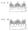
monocrystalline silicon layer 22 of 10 Ωcm in specific resistance and 15 µm thick is grown by means of vapor growth on the surface of a p -typemonocrystalline silicon substrate 21 of 0.005 Ωcm in specific resistance. After thermally 0 treating this silicon layer to form a 1,000 A thermally oxidizedlayer 23 on its main surface, a polycrystalline silicon layer is vapor-grown in POCℓ3 atmosphere on the thermally oxidizedlayer 23 to deposit a 4,000 A phosphorus-dopedpolycrystalline silicon layer 24 as 0 an oxidizable material layer (Fig. 13). Next, a 2,000 A silicon nitride layer is deposited by means of vapor growth directly upon thepolycrystalline silicon layer 24 and a plurality ofsilicon nitride patterns 25 of 2 µm wide (W) and 2 µm pattern pitch (P), for instance, are formed by means of patterning through photo etching process using reactive spatter ion etching. Then, using thesilicon nitride pattern 25 as a mask, boron is ion-implanted under the conditions of 180 KeV and 4 x 10¹³/cm2 dose and then activated to form a p+-type channel stopper 26 on the p-type monocrystalline silicon layer 22 (Fig. 14). In this process, boron may be ion-implanted by using as a mask the photo resist pattern used in the formation of the silicon nitride pattern. - (II) Next, using the
silicon nitride pattern 25 as a oxidation-proof mask, thepolycrystalline silicon layer 24 is selectively oxidized.. In the process, the exposed portions of thepolycrystalline silicon layer 24 is oxidized to form a 8,000 Aoxide layer 27 for element isolation (Fig. 15). No oxynitride layer is recognized to be formed on the surface of the remaining polycrystalline silicon layer 24' along thethick oxide layer 27 below thesilicon nitride pattern 25. In the selective oxidation, moreover, the thermally oxidizedlayer 23 has prevented the phosphorus in thepolycrystalline silicon layer 24 from diffusing into the p-typemonocrystalline silicon layer 22. - (III) Then, after removing the
silicon nitride pattern 25 by means of CF4 dry etching, the remaining polycrystalline silicon layer 24' is removed by means of CCℓ4 reactive spatter ion etching. In the process, as no oxynitride layer exists on the surface of the remaining polycrystalline silicon layer 24', the said polycrystalline silicon layer 24' is perpendicularly etched with self-alignment against thethick oxide layer 26 and apolycrystalline silicon layer 24" is left beneath the overhung of thethick oxide layer 27 as shown in Fig. 16. Next, the thermally oxidized exposedlayer 23 is removed by ammonium fluoride solution to expose part of thepolycrystalline silicon layer 22 and thermal oxidation treatment is carried out. ° In the process, a 400 Agate oxide layer 28 is grown on the exposed surface of thepolycrystalline silicon layer 22 and at the same time thepolycrystalline silicon layer 24" remaining beneath the overhung is oxidized to become an oxide layer to form, together with thethick oxide layer 27, anelement isolation layer 29 without an overhung like the aforementioned thick oxide layer (Fig. 17). Using theelement isolation layer 29 as a mask, boron is ion-implanted into the channel part of the p-type monocrystalline silicon layer below thegate oxide layer 27 under the conditions of 40 KeV output and 3 x 10¹¹/cm2 to produce a p+-type impurities region 30 for the control of threshold value (Fig. 17). - (IV) Then, following the convention process, a
gate electrode 31 consisting of polycrystalline silicon is formed on thegate oxide layer 28, and using thegate electrode 31 as a mask arsenic is ion-implanted and then activated to produce a n+-type source and drain (not shown). After the formation of a CVD-Si02 layer and At wiring, thermal treatment is carried out for 60 minutes at 1,000 °C to produce n channel MOS IC with about 0.8 V in threshold value (Fig. 18). - In this invention, as an element isolation layer is formed by means of selective oxidation of the phosphorus-doped
polycrystalline silicon layer 24 disposed on themonocrystalline silicon layer 22 which is superposed on themonocrystalline silicon layer 21, thermal effects upon themonocrystalline silicon layer 22 can be suppressed and thermal effects to cause defects in themonocrystalline silicon layer 22 and diffusion of impurities into thelayer 22 could be reduced. Also, as the element isolation layer is produced by means of selective oxidation of the phosphorus-dopedpolycrystalline silicon layer 24 on the saidsilicon layer 22 instead of forming it by means of direct oxidation of themonocrystalline silicon layer 22 as in the conventional selective oxidation method, stress upon themonocrystalline silicon layer 22 can be avoided and thus problems of slipping dislocation and defects due to stress could be avoided. - Except for the use of a monocrystalline sapphire substrate instead of the p-type
monocrystalline silicon substrate 21, the exactly same process as Example 3 is employed to produce n channel MOS IC. Figures 14 through 18 may be referred to explain Example 4, assuming that a sapphire substrate is used instead of the p-type monocrystalline silicon substrate. As a phosphorus-doped polycrystalline silicon layer disposed on thesapphire substrate 21 is selectively oxidized, anelement isolation layer 29 of sufficient thickness 0 (8,000 A) can be formed in a considerably shorter time in comparison with selective oxidation of themonocrystalline silicon layer 22. As a result, thermal effects upon thesapphire substrate 21 and themonocrystalline silicon layer 22 can be suppressed. It is also possible to reduce stress due to difference in thermal expansion coefficient and in lattice distance between thesapphire substrate 21 and thesilicon layer 22 and at the same time to reduce the diffusion of impurities into thesilicon layer 22. - This invention can be applied not only to the production of n channel MOS IC.and CMOS IC as discussed above but also to the production of p channel MOS IC, bipolar IC, 12L and CCD.
- As discussed above, it is possible with this invention to produce an element isolation layer, without giving rise to various defects on a semiconductor substrate, by means of selective oxidation of an oxidizable material layer disposed on a semiconductor substrate. It is also possible to control the formation of bird's beak below an oxidation-proof mask during selective oxidation and to produce a finer element isolation layer as no oxynitride layer which behaves as an etching mask is present in the step of removing the oxidizable material layers remaining after the selective oxidation. This invention, therefore, offers a method to produce semiconductor devices having excellent electrical characteristics and which is suitable for making finer semiconductor elements.
Claims (19)
Applications Claiming Priority (12)
| Application Number | Priority Date | Filing Date | Title |
|---|---|---|---|
| JP15614180A JPS5779639A (en) | 1980-11-06 | 1980-11-06 | Manufacture of semiconductor device |
| JP15614080A JPS5779638A (en) | 1980-11-06 | 1980-11-06 | Manufacture of semiconductor device |
| JP156140/80 | 1980-11-06 | ||
| JP156147/80 | 1980-11-06 | ||
| JP156146/80 | 1980-11-06 | ||
| JP15613980A JPS5779637A (en) | 1980-11-06 | 1980-11-06 | Manufacture of semiconductor device |
| JP156141/80 | 1980-11-06 | ||
| JP156139/80 | 1980-11-06 | ||
| JP15614680A JPS5779643A (en) | 1980-11-06 | 1980-11-06 | Semiconductor device |
| JP15614780A JPS5779644A (en) | 1980-11-06 | 1980-11-06 | Manufacture of semiconductor device |
| JP16584380A JPS5790960A (en) | 1980-11-27 | 1980-11-27 | Manufacture of semiconductor device |
| JP165843/80 | 1980-11-27 |
Publications (3)
| Publication Number | Publication Date |
|---|---|
| EP0051488A2 true EP0051488A2 (en) | 1982-05-12 |
| EP0051488A3 EP0051488A3 (en) | 1982-09-22 |
| EP0051488B1 EP0051488B1 (en) | 1985-01-30 |
Family
ID=27553175
Family Applications (1)
| Application Number | Title | Priority Date | Filing Date |
|---|---|---|---|
| EP81305215A Expired EP0051488B1 (en) | 1980-11-06 | 1981-11-02 | Method for manufacturing a semiconductor device |
Country Status (3)
| Country | Link |
|---|---|
| US (1) | US4459325A (en) |
| EP (1) | EP0051488B1 (en) |
| DE (1) | DE3168688D1 (en) |
Families Citing this family (45)
| Publication number | Priority date | Publication date | Assignee | Title |
|---|---|---|---|---|
| DE3330895A1 (en) * | 1983-08-26 | 1985-03-14 | Siemens AG, 1000 Berlin und 8000 München | METHOD FOR PRODUCING BIPOLAR TRANSISTOR STRUCTURES WITH SELF-ADJUSTED EMITTER AND BASE AREAS FOR HIGH-FREQUENCY CIRCUITS |
| US4716131A (en) * | 1983-11-28 | 1987-12-29 | Nec Corporation | Method of manufacturing semiconductor device having polycrystalline silicon layer with metal silicide film |
| JPS60244072A (en) * | 1984-05-17 | 1985-12-03 | Toshiba Corp | Manufacture of semiconductor device |
| JPS61191043A (en) * | 1985-02-20 | 1986-08-25 | Toshiba Corp | Semiconductor device |
| US4613402A (en) * | 1985-07-01 | 1986-09-23 | Eastman Kodak Company | Method of making edge-aligned implants and electrodes therefor |
| US4968640A (en) * | 1987-02-10 | 1990-11-06 | Industrial Technology Research Institute | Isolation structures for integrated circuits |
| US5114833A (en) * | 1988-08-29 | 1992-05-19 | Eastman Kodak Company | Charge-coupled device and process of making the device |
| US5175123A (en) * | 1990-11-13 | 1992-12-29 | Motorola, Inc. | High-pressure polysilicon encapsulated localized oxidation of silicon |
| KR0172816B1 (en) * | 1991-01-14 | 1999-03-30 | 문정환 | Method for fabricating mask |
| US5460908A (en) * | 1991-08-02 | 1995-10-24 | Micron Technology, Inc. | Phase shifting retical fabrication method |
| US5580815A (en) * | 1993-08-12 | 1996-12-03 | Motorola Inc. | Process for forming field isolation and a structure over a semiconductor substrate |
| US5972746A (en) * | 1996-10-08 | 1999-10-26 | Mosel Vitelic, Inc. | Method for manufacturing semiconductor devices using double-charged implantation |
| US6096660A (en) * | 1997-08-21 | 2000-08-01 | Micron Technology, Inc. | Method for removing undesirable second oxide while minimally affecting a desirable first oxide |
| US6392257B1 (en) | 2000-02-10 | 2002-05-21 | Motorola Inc. | Semiconductor structure, semiconductor device, communicating device, integrated circuit, and process for fabricating the same |
| US6693033B2 (en) | 2000-02-10 | 2004-02-17 | Motorola, Inc. | Method of removing an amorphous oxide from a monocrystalline surface |
| WO2001093336A1 (en) | 2000-05-31 | 2001-12-06 | Motorola, Inc. | Semiconductor device and method for manufacturing the same |
| AU2001264987A1 (en) * | 2000-06-30 | 2002-01-14 | Motorola, Inc., A Corporation Of The State Of Delware | Hybrid semiconductor structure and device |
| US6555946B1 (en) | 2000-07-24 | 2003-04-29 | Motorola, Inc. | Acoustic wave device and process for forming the same |
| US6590236B1 (en) | 2000-07-24 | 2003-07-08 | Motorola, Inc. | Semiconductor structure for use with high-frequency signals |
| AU2001277001A1 (en) | 2000-07-24 | 2002-02-05 | Motorola, Inc. | Heterojunction tunneling diodes and process for fabricating same |
| US6493497B1 (en) | 2000-09-26 | 2002-12-10 | Motorola, Inc. | Electro-optic structure and process for fabricating same |
| US6638838B1 (en) | 2000-10-02 | 2003-10-28 | Motorola, Inc. | Semiconductor structure including a partially annealed layer and method of forming the same |
| US6501121B1 (en) | 2000-11-15 | 2002-12-31 | Motorola, Inc. | Semiconductor structure |
| US6559471B2 (en) | 2000-12-08 | 2003-05-06 | Motorola, Inc. | Quantum well infrared photodetector and method for fabricating same |
| US20020096683A1 (en) | 2001-01-19 | 2002-07-25 | Motorola, Inc. | Structure and method for fabricating GaN devices utilizing the formation of a compliant substrate |
| US6673646B2 (en) | 2001-02-28 | 2004-01-06 | Motorola, Inc. | Growth of compound semiconductor structures on patterned oxide films and process for fabricating same |
| WO2002082551A1 (en) | 2001-04-02 | 2002-10-17 | Motorola, Inc. | A semiconductor structure exhibiting reduced leakage current |
| US6709989B2 (en) | 2001-06-21 | 2004-03-23 | Motorola, Inc. | Method for fabricating a semiconductor structure including a metal oxide interface with silicon |
| US6992321B2 (en) | 2001-07-13 | 2006-01-31 | Motorola, Inc. | Structure and method for fabricating semiconductor structures and devices utilizing piezoelectric materials |
| US6531740B2 (en) | 2001-07-17 | 2003-03-11 | Motorola, Inc. | Integrated impedance matching and stability network |
| US6646293B2 (en) | 2001-07-18 | 2003-11-11 | Motorola, Inc. | Structure for fabricating high electron mobility transistors utilizing the formation of complaint substrates |
| US6693298B2 (en) | 2001-07-20 | 2004-02-17 | Motorola, Inc. | Structure and method for fabricating epitaxial semiconductor on insulator (SOI) structures and devices utilizing the formation of a compliant substrate for materials used to form same |
| US7019332B2 (en) | 2001-07-20 | 2006-03-28 | Freescale Semiconductor, Inc. | Fabrication of a wavelength locker within a semiconductor structure |
| US6855992B2 (en) | 2001-07-24 | 2005-02-15 | Motorola Inc. | Structure and method for fabricating configurable transistor devices utilizing the formation of a compliant substrate for materials used to form the same |
| US6667196B2 (en) | 2001-07-25 | 2003-12-23 | Motorola, Inc. | Method for real-time monitoring and controlling perovskite oxide film growth and semiconductor structure formed using the method |
| US6589856B2 (en) | 2001-08-06 | 2003-07-08 | Motorola, Inc. | Method and apparatus for controlling anti-phase domains in semiconductor structures and devices |
| US6639249B2 (en) | 2001-08-06 | 2003-10-28 | Motorola, Inc. | Structure and method for fabrication for a solid-state lighting device |
| US20030034491A1 (en) | 2001-08-14 | 2003-02-20 | Motorola, Inc. | Structure and method for fabricating semiconductor structures and devices for detecting an object |
| US6673667B2 (en) | 2001-08-15 | 2004-01-06 | Motorola, Inc. | Method for manufacturing a substantially integral monolithic apparatus including a plurality of semiconductor materials |
| US20030071327A1 (en) | 2001-10-17 | 2003-04-17 | Motorola, Inc. | Method and apparatus utilizing monocrystalline insulator |
| US6916717B2 (en) | 2002-05-03 | 2005-07-12 | Motorola, Inc. | Method for growing a monocrystalline oxide layer and for fabricating a semiconductor device on a monocrystalline substrate |
| US7169619B2 (en) | 2002-11-19 | 2007-01-30 | Freescale Semiconductor, Inc. | Method for fabricating semiconductor structures on vicinal substrates using a low temperature, low pressure, alkaline earth metal-rich process |
| US6885065B2 (en) | 2002-11-20 | 2005-04-26 | Freescale Semiconductor, Inc. | Ferromagnetic semiconductor structure and method for forming the same |
| US7020374B2 (en) | 2003-02-03 | 2006-03-28 | Freescale Semiconductor, Inc. | Optical waveguide structure and method for fabricating the same |
| US6965128B2 (en) | 2003-02-03 | 2005-11-15 | Freescale Semiconductor, Inc. | Structure and method for fabricating semiconductor microresonator devices |
Citations (3)
| Publication number | Priority date | Publication date | Assignee | Title |
|---|---|---|---|---|
| GB1437112A (en) * | 1973-09-07 | 1976-05-26 | Mullard Ltd | Semiconductor device manufacture |
| GB1501249A (en) * | 1974-11-06 | 1978-02-15 | Ibm | Field effect transistor |
| EP0015677A1 (en) * | 1979-02-28 | 1980-09-17 | Vlsi Technology Research Association | Method of producing semiconductor devices |
Family Cites Families (3)
| Publication number | Priority date | Publication date | Assignee | Title |
|---|---|---|---|---|
| US3753803A (en) * | 1968-12-06 | 1973-08-21 | Hitachi Ltd | Method of dividing semiconductor layer into a plurality of isolated regions |
| US4137109A (en) * | 1976-04-12 | 1979-01-30 | Texas Instruments Incorporated | Selective diffusion and etching method for isolation of integrated logic circuit |
| FR2459551A1 (en) * | 1979-06-19 | 1981-01-09 | Thomson Csf | SELF-ALIGNMENT PASSIVATION METHOD AND STRUCTURE ON THE PLACE OF A MASK |
-
1981
- 1981-11-02 EP EP81305215A patent/EP0051488B1/en not_active Expired
- 1981-11-02 DE DE8181305215T patent/DE3168688D1/en not_active Expired
- 1981-11-03 US US06/317,616 patent/US4459325A/en not_active Expired - Lifetime
Patent Citations (3)
| Publication number | Priority date | Publication date | Assignee | Title |
|---|---|---|---|---|
| GB1437112A (en) * | 1973-09-07 | 1976-05-26 | Mullard Ltd | Semiconductor device manufacture |
| GB1501249A (en) * | 1974-11-06 | 1978-02-15 | Ibm | Field effect transistor |
| EP0015677A1 (en) * | 1979-02-28 | 1980-09-17 | Vlsi Technology Research Association | Method of producing semiconductor devices |
Non-Patent Citations (3)
| Title |
|---|
| IBM Technica Disclosure Bulletin Vol. 21, No. 12, May 1979 New York I. ANTIPOV "Mask-Independent Short Channel MOS" pages 4852 to 4854 * page 4854, steps 5, 6 * * |
| IBM Technical Disclosure Bulletin Vol. 17, No. 3, August 1974 New York V.L. RIDEOUT et al. "Fabricating Recessed Oxide Isolation Regions in silicon substrates" pages 949 to 951 * page 950, third paragraph * * |
| IBM TECHNICAL DISCLOSURE BULLETIN, vol. 21, no. 12, May 1979, New York, I. ANTIPOV "Mask-independent short channel MOS", pages 4852 to 4854 * |
Also Published As
| Publication number | Publication date |
|---|---|
| EP0051488A3 (en) | 1982-09-22 |
| DE3168688D1 (en) | 1985-03-14 |
| US4459325A (en) | 1984-07-10 |
| EP0051488B1 (en) | 1985-01-30 |
Similar Documents
| Publication | Publication Date | Title |
|---|---|---|
| US4459325A (en) | Semiconductor device and method for manufacturing the same | |
| EP0146895B1 (en) | Method of manufacturing semiconductor device | |
| US4642878A (en) | Method of making MOS device by sequentially depositing an oxidizable layer and a masking second layer over gated device regions | |
| US4749441A (en) | Semiconductor mushroom structure fabrication | |
| US4170492A (en) | Method of selective oxidation in manufacture of semiconductor devices | |
| US4891328A (en) | Method of manufacturing field effect transistors and lateral bipolar transistors on the same substrate | |
| KR20010012906A (en) | Integrated circuit, components thereof and manufacturing method | |
| US5895252A (en) | Field oxidation by implanted oxygen (FIMOX) | |
| US4372033A (en) | Method of making coplanar MOS IC structures | |
| US5106768A (en) | Method for the manufacture of CMOS FET by P+ maskless technique | |
| US5219783A (en) | Method of making semiconductor well structure | |
| JP2785919B2 (en) | Method of manufacturing semiconductor device having growth layer on insulating layer | |
| EP0126292B1 (en) | Semiconductor device having an element isolation layer and method of manufacturing the same | |
| JP3060948B2 (en) | Method for manufacturing semiconductor device | |
| KR0140444B1 (en) | Manufacture of bipolar device | |
| GB2218848A (en) | A method of fabricating semiconductor devices | |
| KR100216510B1 (en) | Fabrication method of the collector for a bipolar transistor using a trench | |
| KR100209765B1 (en) | Method of fabricating bi-mos | |
| JPH0338742B2 (en) | ||
| KR910008978B1 (en) | Manufacturing method of semiconductor device | |
| JPH0223028B2 (en) | ||
| JPH0423828B2 (en) | ||
| JPH1092922A (en) | Semiconductor device and manufacture thereof | |
| KR0126645B1 (en) | Isolation oxide film forming method of semiconductor device | |
| JPH023306B2 (en) |
Legal Events
| Date | Code | Title | Description |
|---|---|---|---|
| PUAI | Public reference made under article 153(3) epc to a published international application that has entered the european phase |
Free format text: ORIGINAL CODE: 0009012 |
|
| 17P | Request for examination filed |
Effective date: 19811110 |
|
| AK | Designated contracting states |
Designated state(s): DE FR GB NL |
|
| PUAL | Search report despatched |
Free format text: ORIGINAL CODE: 0009013 |
|
| AK | Designated contracting states |
Designated state(s): DE FR GB NL |
|
| RAP1 | Party data changed (applicant data changed or rights of an application transferred) |
Owner name: KABUSHIKI KAISHA TOSHIBA |
|
| GRAA | (expected) grant |
Free format text: ORIGINAL CODE: 0009210 |
|
| AK | Designated contracting states |
Designated state(s): DE FR GB NL |
|
| REF | Corresponds to: |
Ref document number: 3168688 Country of ref document: DE Date of ref document: 19850314 |
|
| ET | Fr: translation filed | ||
| PLBE | No opposition filed within time limit |
Free format text: ORIGINAL CODE: 0009261 |
|
| STAA | Information on the status of an ep patent application or granted ep patent |
Free format text: STATUS: NO OPPOSITION FILED WITHIN TIME LIMIT |
|
| 26N | No opposition filed | ||
| REG | Reference to a national code |
Ref country code: GB Ref legal event code: 746 |
|
| PGFP | Annual fee paid to national office [announced via postgrant information from national office to epo] |
Ref country code: GB Payment date: 19971024 Year of fee payment: 17 |
|
| PGFP | Annual fee paid to national office [announced via postgrant information from national office to epo] |
Ref country code: DE Payment date: 19971110 Year of fee payment: 17 |
|
| PGFP | Annual fee paid to national office [announced via postgrant information from national office to epo] |
Ref country code: FR Payment date: 19971112 Year of fee payment: 17 |
|
| PG25 | Lapsed in a contracting state [announced via postgrant information from national office to epo] |
Ref country code: GB Free format text: LAPSE BECAUSE OF NON-PAYMENT OF DUE FEES Effective date: 19981102 |
|
| GBPC | Gb: european patent ceased through non-payment of renewal fee |
Effective date: 19981102 |
|
| PG25 | Lapsed in a contracting state [announced via postgrant information from national office to epo] |
Ref country code: FR Free format text: LAPSE BECAUSE OF NON-PAYMENT OF DUE FEES Effective date: 19990730 |
|
| REG | Reference to a national code |
Ref country code: FR Ref legal event code: ST |
|
| PG25 | Lapsed in a contracting state [announced via postgrant information from national office to epo] |
Ref country code: DE Free format text: LAPSE BECAUSE OF NON-PAYMENT OF DUE FEES Effective date: 19990901 |
|
| PGFP | Annual fee paid to national office [announced via postgrant information from national office to epo] |
Ref country code: NL Payment date: 19991130 Year of fee payment: 19 |
|
| PG25 | Lapsed in a contracting state [announced via postgrant information from national office to epo] |
Ref country code: NL Free format text: LAPSE BECAUSE OF NON-PAYMENT OF DUE FEES Effective date: 20010601 |
|
| NLV4 | Nl: lapsed or anulled due to non-payment of the annual fee |
Effective date: 20010601 |