EP0032801A2 - Method of dicing a semiconductor wafer - Google Patents
Method of dicing a semiconductor wafer Download PDFInfo
- Publication number
- EP0032801A2 EP0032801A2 EP19810300122 EP81300122A EP0032801A2 EP 0032801 A2 EP0032801 A2 EP 0032801A2 EP 19810300122 EP19810300122 EP 19810300122 EP 81300122 A EP81300122 A EP 81300122A EP 0032801 A2 EP0032801 A2 EP 0032801A2
- Authority
- EP
- European Patent Office
- Prior art keywords
- dicing
- dicing line
- semiconductor wafer
- cracks
- forming
- Prior art date
- Legal status (The legal status is an assumption and is not a legal conclusion. Google has not performed a legal analysis and makes no representation as to the accuracy of the status listed.)
- Granted
Links
Images


Classifications
-
- H—ELECTRICITY
- H01—ELECTRIC ELEMENTS
- H01L—SEMICONDUCTOR DEVICES NOT COVERED BY CLASS H10
- H01L21/00—Processes or apparatus adapted for the manufacture or treatment of semiconductor or solid state devices or of parts thereof
- H01L21/02—Manufacture or treatment of semiconductor devices or of parts thereof
- H01L21/04—Manufacture or treatment of semiconductor devices or of parts thereof the devices having at least one potential-jump barrier or surface barrier, e.g. PN junction, depletion layer or carrier concentration layer
- H01L21/18—Manufacture or treatment of semiconductor devices or of parts thereof the devices having at least one potential-jump barrier or surface barrier, e.g. PN junction, depletion layer or carrier concentration layer the devices having semiconductor bodies comprising elements of Group IV of the Periodic System or AIIIBV compounds with or without impurities, e.g. doping materials
- H01L21/30—Treatment of semiconductor bodies using processes or apparatus not provided for in groups H01L21/20 - H01L21/26
- H01L21/302—Treatment of semiconductor bodies using processes or apparatus not provided for in groups H01L21/20 - H01L21/26 to change their surface-physical characteristics or shape, e.g. etching, polishing, cutting
- H01L21/304—Mechanical treatment, e.g. grinding, polishing, cutting
- H01L21/3043—Making grooves, e.g. cutting
-
- Y—GENERAL TAGGING OF NEW TECHNOLOGICAL DEVELOPMENTS; GENERAL TAGGING OF CROSS-SECTIONAL TECHNOLOGIES SPANNING OVER SEVERAL SECTIONS OF THE IPC; TECHNICAL SUBJECTS COVERED BY FORMER USPC CROSS-REFERENCE ART COLLECTIONS [XRACs] AND DIGESTS
- Y10—TECHNICAL SUBJECTS COVERED BY FORMER USPC
- Y10S—TECHNICAL SUBJECTS COVERED BY FORMER USPC CROSS-REFERENCE ART COLLECTIONS [XRACs] AND DIGESTS
- Y10S148/00—Metal treatment
- Y10S148/028—Dicing
-
- Y—GENERAL TAGGING OF NEW TECHNOLOGICAL DEVELOPMENTS; GENERAL TAGGING OF CROSS-SECTIONAL TECHNOLOGIES SPANNING OVER SEVERAL SECTIONS OF THE IPC; TECHNICAL SUBJECTS COVERED BY FORMER USPC CROSS-REFERENCE ART COLLECTIONS [XRACs] AND DIGESTS
- Y10—TECHNICAL SUBJECTS COVERED BY FORMER USPC
- Y10T—TECHNICAL SUBJECTS COVERED BY FORMER US CLASSIFICATION
- Y10T225/00—Severing by tearing or breaking
- Y10T225/10—Methods
- Y10T225/12—With preliminary weakening
-
- Y—GENERAL TAGGING OF NEW TECHNOLOGICAL DEVELOPMENTS; GENERAL TAGGING OF CROSS-SECTIONAL TECHNOLOGIES SPANNING OVER SEVERAL SECTIONS OF THE IPC; TECHNICAL SUBJECTS COVERED BY FORMER USPC CROSS-REFERENCE ART COLLECTIONS [XRACs] AND DIGESTS
- Y10—TECHNICAL SUBJECTS COVERED BY FORMER USPC
- Y10T—TECHNICAL SUBJECTS COVERED BY FORMER US CLASSIFICATION
- Y10T29/00—Metal working
- Y10T29/49—Method of mechanical manufacture
- Y10T29/49789—Obtaining plural product pieces from unitary workpiece
- Y10T29/4979—Breaking through weakened portion
-
- Y—GENERAL TAGGING OF NEW TECHNOLOGICAL DEVELOPMENTS; GENERAL TAGGING OF CROSS-SECTIONAL TECHNOLOGIES SPANNING OVER SEVERAL SECTIONS OF THE IPC; TECHNICAL SUBJECTS COVERED BY FORMER USPC CROSS-REFERENCE ART COLLECTIONS [XRACs] AND DIGESTS
- Y10—TECHNICAL SUBJECTS COVERED BY FORMER USPC
- Y10T—TECHNICAL SUBJECTS COVERED BY FORMER US CLASSIFICATION
- Y10T29/00—Metal working
- Y10T29/49—Method of mechanical manufacture
- Y10T29/49789—Obtaining plural product pieces from unitary workpiece
- Y10T29/49792—Dividing through modified portion
Landscapes
- Engineering & Computer Science (AREA)
- Physics & Mathematics (AREA)
- Condensed Matter Physics & Semiconductors (AREA)
- General Physics & Mathematics (AREA)
- Manufacturing & Machinery (AREA)
- Computer Hardware Design (AREA)
- Microelectronics & Electronic Packaging (AREA)
- Power Engineering (AREA)
- Dicing (AREA)
- Structure Of Printed Boards (AREA)
Abstract

Description
- This invention relates to a method of dicing a semiconductor wafer.
- With most semiconductor products, for example, transistors, diodes, light emitting diodes, and integrated circuits, a large number of elements are manufactured simultaneously on a large semiconductor wafer of Si, GaP, GaAs, sapphire etc. The semiconductor industry employs the term "dicing technologies" to refer to those techniques for dividing up a semiconductor wafer to obtain a large number of high quality pellets. Two dicing methods are particularly well known in the art. These are the grinding-cutting method, using a wire bladed saw, and the scribing method, using a diamond point. When laying out the pattern of pellets on the surface of the semiconductor wafer, the distance between adjacent pellets has been minimized to maximize efficiency.
- However, there are three restrictions upon the minimum distance attainable between adjacent pellets. The first restriction is the actual dicing width, the second restriction is the degree of precision to which the cutting machine can be adjusted, and the third restriction is the extent of the cracks and chips extending horizontally from the dicing line. Of these restrictions, the third, namely the generation of cracks and chips, creates the most significant limitation with respect to minimising the distance between adjacent pellets.
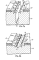
- FIGURE la illustrates the effect of the traditional grinding-cutting method, and FIGURE lb illustrates the effect of the traditional scribing method. Similar elements in these FIGURES are assigned the same reference numbers. A
semiconductor substrate 11 carries many active element areas such as 12, 13 (not shown in detail), and dicing occurs in the space between the adjacentactive element areas chips 14 are generated horizontsally from adicing line 15. Therefore, the distance betweenactive element areas 12, 13 (shown in FIGURES la and Ib as distance A-A) has to be 100-200 µm to prevent theactive element areas chips 14. - This invention seeks to provide an improved method of dicing a semiconductor wafer to prevent cracks and chips along the dicing line from spreading to the active areas.
- The method of dicing the semiconductor wafer according to this invention includes the step of forming a physical discontinuity on the surface of the wafer on both sides of a predetermined dicing lane. The semiconductor wafer is then diced into pellets
- Some embodiments of the invention will now be described by way of example with reference to the accompanying drawings, in which:
- FIGURES la and lb are partly sectional, enlarged perspective views of a device manufactured by conventional techniques;
- FIGURES 2a and 2b are partly sectional, enlarged perspective views of devices manufactured by methods of this invention;
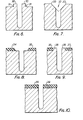
- FIGURES 3 to 5, inclusive are enlarged sectional views respectively, showing the principles of this invention and devices manufactured by other methods of this invention; and
- FIGURES 6 to 10, inclusive are enlarged partly sectional views of devices manufactured by still other methods of this invention.
- Cracks and chips which are generated during dicing generally propagate in a direction perpendicular to the direction of maximum stress in the wafer. Thus, typically, cracks spread away from the dicing line into the wafer. However we have found that this propagation can be restrained by the formation of a stress concentration in the path of the crack. Thus, the transmission of the cracks and chips can be restrained by the formation of a physical discontinuity on the surface of the wafer on both sides of a predetermined dicing line.
- Referring now to the drawings wherein like reference characters designate like or corresponding parts throughout the several views, FIGURES 2a and 2b illustrate the effects of this invention, with FIGURE 2a illustrating the effect of the grinding cutting method and FIGURE 2b illustrating the effect of the scribing method.
Active element areas substrate 23 and many circuit elements (not shown) are manufactured in these areas. A change in the level of the surface ofsubstrate 23, specifically a groove defined bywalls substrate 23. The distance betweenwalls 24, 25 (shown in FIGURES 2a and 2b as distance B-B) is 60 µm, and the height ofwalls walls substrate 23 is ground or scribed along the predetermined line to form the deep groove 40 in FIGURE 2a or theshallow groove 41 in FIGURE 2b respectively. As a result of this invention, the transmission of cracks andchips 26 is stopped atwalls - FIGURE 3 illustrates the path of propagation of cracks and chips into
substrate 23 in the cutting- grinding embodiments of this invention. A crack generated at point A spreads via point B to point C wherewall 24 stops the spreading. In the absence ofwall 24, the crack would have extended to point D alongdotted line 27. The reason the crack stops at point C is as follows. The crack generated at the point A will tend to spread perpendicular to the direction of the main stress, tht is into the substrate, roughly parallel to the surface. When the front of the crack reaches point B,wall 24 causes the concentration of stress to occur between point B and point C. Thus the crack tends to change direction and proceed to the surface, stopping at point C. - In another embodiment of this invention, as shown in FIGURE 4, a surface level change, specifically a
groove 28 is created to concentrate the stress. Cracks generated at the point E and H spread to points F and I, respectively, and stop. Groove 28 may have a depth of 3 or 4 µm. FIGURE 5 shows another embodiment of this invention, which includes the step of forming asemiconductor oxide film 29 on and partially into the substrate to create a surface level change. For cracks generated at points J and L, the stress concentrations happen between points K and M, respectively, so that the cracks are restrained at points K and M. - FIGURES 6 to 10 illustrate the product of other embodiments of this invention. Referring to FIGURE 6, a surface level change, specifically a
protuberance 30 is formed on the surface along and extending beyond the predtermined dicing line. Cracks are restrained atwalls 31. In FIGURE 7, a V-shaped notch 32 is formed over the predetermined dicing line, and cracks are restrained atedges 33 ofnotch 32, because these edges comprise a surface level change. In FIGURE 8,oxide films 34, 35 are formed on the surface, on both sides of the dicing line. Cracks are restrained at the edges of these oxide films. FIGURE 9 illustrates the product of another ambodiment of this invention, which combines the embodiments shown in FIGURES 6 and 8.Oxide films protuberance 38, and cracks are restrained more certainly by these stress concentration portions. In FIGURE 10, a uniformthermal oxide film 39 is formed on the surface of the substrate including the predetermined dicing line and adjacent thereto. Almot all of the cracks from the dicing operation are transmitted intooxide film 39, so that the substrate is not influenced. The thickness ofoxide film 39 is preferably 200-600 Angstroms to ensure that the substrate is not disturbed. - In the above-mentioned embodiments of this invention, the physical discontinuities must be formed on both sides of the predetermined dicing line. Therefore, cracks and chips are restrained and stopped by the above mentioned physical discontinuities. The different materials used as the physical discontinuites are suitable films having good adhesion and affinity characteristics, for example, thermal oxide film, nitride film and metal film.
- Many changes and modifications in the above described embodiments can, of course, be carried out without departing from the scope of the present invention, that scope being defined only by the scope of the appended claims.
Claims (6)
Applications Claiming Priority (2)
| Application Number | Priority Date | Filing Date | Title |
|---|---|---|---|
| JP607980A JPS56103447A (en) | 1980-01-22 | 1980-01-22 | Dicing method of semiconductor wafer |
| JP6079/80 | 1980-01-22 |
Publications (3)
| Publication Number | Publication Date |
|---|---|
| EP0032801A2 true EP0032801A2 (en) | 1981-07-29 |
| EP0032801A3 EP0032801A3 (en) | 1982-11-03 |
| EP0032801B1 EP0032801B1 (en) | 1986-09-03 |
Family
ID=11628550
Family Applications (1)
| Application Number | Title | Priority Date | Filing Date |
|---|---|---|---|
| EP19810300122 Expired EP0032801B1 (en) | 1980-01-22 | 1981-01-13 | Method of dicing a semiconductor wafer |
Country Status (4)
| Country | Link |
|---|---|
| US (1) | US4610079A (en) |
| EP (1) | EP0032801B1 (en) |
| JP (1) | JPS56103447A (en) |
| DE (2) | DE3175244D1 (en) |
Cited By (5)
| Publication number | Priority date | Publication date | Assignee | Title |
|---|---|---|---|---|
| EP0220404A1 (en) * | 1985-09-30 | 1987-05-06 | Siemens Aktiengesellschaft | Method of limiting chippage during the sawing of a semiconductor disc |
| US4929300A (en) * | 1988-08-05 | 1990-05-29 | Siemens Aktiengesellschaft | Process for the separation of monolithic LED chip arrangements generated on a semiconductor substrate wafer |
| EP0678904A1 (en) * | 1994-04-12 | 1995-10-25 | Lsi Logic Corporation | Multicut wafer saw process |
| DE10218498A1 (en) * | 2002-04-25 | 2003-11-20 | Osram Opto Semiconductors Gmbh | Production of a semiconductor layer comprises preparing a substrate, applying a mask layer having openings on the substrate, and growing a semiconductor layer |
| US9536831B2 (en) | 2015-05-12 | 2017-01-03 | United Microelectronics Corp. | Semiconductor device and method for fabricating the same |
Families Citing this family (57)
| Publication number | Priority date | Publication date | Assignee | Title |
|---|---|---|---|---|
| GB2172141B (en) * | 1985-03-08 | 1988-11-16 | Stc Plc | Single heterostructure laser chip manufacture |
| JPH0716077B2 (en) * | 1985-10-11 | 1995-02-22 | 三菱電機株式会社 | Method of manufacturing semiconductor laser device |
| US4814296A (en) * | 1987-08-28 | 1989-03-21 | Xerox Corporation | Method of fabricating image sensor dies for use in assembling arrays |
| US5240882A (en) * | 1988-06-28 | 1993-08-31 | Naoetsu Electronics Co. | Process and apparatus for making discrete type substrates by re-slicing a wafer |
| JPH0750700B2 (en) * | 1989-06-27 | 1995-05-31 | 三菱電機株式会社 | Semiconductor chip manufacturing method |
| US4966862A (en) * | 1989-08-28 | 1990-10-30 | Cree Research, Inc. | Method of production of light emitting diodes |
| US4997792A (en) * | 1989-11-21 | 1991-03-05 | Eastman Kodak Company | Method for separation of diode array chips during fabrication thereof |
| US5053836A (en) * | 1989-11-21 | 1991-10-01 | Eastman Kodak Company | Cleaving of diode arrays with scribing channels |
| US4997793A (en) * | 1989-11-21 | 1991-03-05 | Eastman Kodak Company | Method of improving cleaving of diode arrays |
| US5098503A (en) * | 1990-05-01 | 1992-03-24 | Xerox Corporation | Method of fabricating precision pagewidth assemblies of ink jet subunits |
| US5206181A (en) * | 1991-06-03 | 1993-04-27 | Motorola, Inc. | Method for manufacturing a semiconductor device with a slotted metal test pad to prevent lift-off during wafer scribing |
| JP2763441B2 (en) * | 1992-02-06 | 1998-06-11 | 三菱電機株式会社 | Method for manufacturing semiconductor device |
| US5259925A (en) * | 1992-06-05 | 1993-11-09 | Mcdonnell Douglas Corporation | Method of cleaning a plurality of semiconductor devices |
| US5552345A (en) * | 1993-09-22 | 1996-09-03 | Harris Corporation | Die separation method for silicon on diamond circuit structures |
| US5420455A (en) * | 1994-03-31 | 1995-05-30 | International Business Machines Corp. | Array fuse damage protection devices and fabrication method |
| US5599746A (en) * | 1994-05-06 | 1997-02-04 | United Microelectronics Corporation | Method to eliminate polycide peeling at wafer edge using extended scribe lines |
| US5543365A (en) * | 1994-12-02 | 1996-08-06 | Texas Instruments Incorporated | Wafer scribe technique using laser by forming polysilicon |
| US5882988A (en) * | 1995-08-16 | 1999-03-16 | Philips Electronics North America Corporation | Semiconductor chip-making without scribing |
| US5710538A (en) * | 1995-09-27 | 1998-01-20 | Micrel, Inc. | Circuit having trim pads formed in scribe channel |
| JPH09172223A (en) * | 1995-12-19 | 1997-06-30 | Sony Corp | Semiconductor device and its manufacture |
| JPH09306872A (en) * | 1996-05-14 | 1997-11-28 | Sony Corp | Semiconductor device |
| US6107161A (en) * | 1996-06-07 | 2000-08-22 | Rohm Co., Ltd. | Semiconductor chip and a method for manufacturing thereof |
| CN1097849C (en) * | 1996-06-07 | 2003-01-01 | 罗姆股份有限公司 | Semiconductor chip and method for manufacturing the same |
| US5834829A (en) * | 1996-09-05 | 1998-11-10 | International Business Machines Corporation | Energy relieving crack stop |
| WO1998013862A1 (en) * | 1996-09-24 | 1998-04-02 | Mitsubishi Denki Kabushiki Kaisha | Semiconductor device and production method thereof |
| US5789302A (en) * | 1997-03-24 | 1998-08-04 | Siemens Aktiengesellschaft | Crack stops |
| US6430810B1 (en) | 1997-10-28 | 2002-08-13 | Uniax Corporation | Mechanical scribing methods of forming a patterned metal layer in an electronic device |
| US6093624A (en) * | 1997-12-23 | 2000-07-25 | Philips Electronics North America Corporation | Method of providing a gettering scheme in the manufacture of silicon-on-insulator (SOI) integrated circuits |
| JP3497722B2 (en) * | 1998-02-27 | 2004-02-16 | 富士通株式会社 | Semiconductor device, method of manufacturing the same, and transfer tray thereof |
| JP2001102486A (en) * | 1999-07-28 | 2001-04-13 | Seiko Epson Corp | Substrate for semiconductor device, semiconductor-chip mounting substrate, semiconductor device, their manufacturing method, circuit board and electronic device |
| US6717245B1 (en) | 2000-06-02 | 2004-04-06 | Micron Technology, Inc. | Chip scale packages performed by wafer level processing |
| US6676878B2 (en) | 2001-01-31 | 2004-01-13 | Electro Scientific Industries, Inc. | Laser segmented cutting |
| JP3928695B2 (en) * | 2001-03-30 | 2007-06-13 | セイコーエプソン株式会社 | Surface emitting semiconductor light emitting device and method of manufacturing the same |
| US6895133B1 (en) * | 2001-06-20 | 2005-05-17 | Lightwave Microsystems Corporation | Crack propagation stops for dicing of planar lightwave circuit devices |
| JP2003151924A (en) * | 2001-08-28 | 2003-05-23 | Tokyo Seimitsu Co Ltd | Dicing method and dicing apparatus |
| SG139508A1 (en) | 2001-09-10 | 2008-02-29 | Micron Technology Inc | Wafer dicing device and method |
| SG102639A1 (en) * | 2001-10-08 | 2004-03-26 | Micron Technology Inc | Apparatus and method for packing circuits |
| JP2005523583A (en) | 2002-04-19 | 2005-08-04 | エグシル テクノロジー リミテッド | Programmed dicing of substrates using pulsed laser |
| SG142115A1 (en) | 2002-06-14 | 2008-05-28 | Micron Technology Inc | Wafer level packaging |
| SG119185A1 (en) * | 2003-05-06 | 2006-02-28 | Micron Technology Inc | Method for packaging circuits and packaged circuits |
| US20050026397A1 (en) * | 2003-07-28 | 2005-02-03 | International Business Machines Corporation | Crack stop for low k dielectrics |
| JP4422463B2 (en) * | 2003-11-07 | 2010-02-24 | 株式会社ディスコ | Semiconductor wafer dividing method |
| JP2005195965A (en) * | 2004-01-08 | 2005-07-21 | Sharp Corp | Hologram element, manufacturing method therefor, and electro-optical component |
| GB2420443B (en) * | 2004-11-01 | 2009-09-16 | Xsil Technology Ltd | Increasing die strength by etching during or after dicing |
| US7268440B2 (en) * | 2005-01-09 | 2007-09-11 | United Microelectronics Corp. | Fabrication of semiconductor integrated circuit chips |
| US20060278957A1 (en) * | 2005-06-09 | 2006-12-14 | Zong-Huei Lin | Fabrication of semiconductor integrated circuit chips |
| DE102005046479B4 (en) * | 2005-09-28 | 2008-12-18 | Infineon Technologies Austria Ag | Process for splitting brittle materials using trenching technology |
| FR2893182B1 (en) * | 2005-11-10 | 2007-12-28 | Atmel Grenoble Soc Par Actions | INTEGRATED CIRCUIT CHIP CUTTING METHOD ON AMINCI SUBSTRATE |
| CN101346857A (en) * | 2005-12-26 | 2009-01-14 | 松下电器产业株式会社 | Nitride compound semiconductor element and method for manufacturing same |
| KR100711882B1 (en) * | 2006-01-27 | 2007-04-25 | 삼성에스디아이 주식회사 | Method for manufacturing organic light emitting display |
| JP4743661B2 (en) * | 2006-03-07 | 2011-08-10 | 信越半導体株式会社 | Light emitting device manufacturing method and light emitting device |
| US8102027B2 (en) * | 2007-08-21 | 2012-01-24 | Broadcom Corporation | IC package sacrificial structures for crack propagation confinement |
| US8698004B2 (en) | 2008-10-27 | 2014-04-15 | Ibiden Co., Ltd. | Multi-piece board and fabrication method thereof |
| US9917011B2 (en) * | 2014-05-19 | 2018-03-13 | Sharp Kabushiki Kaisha | Semiconductor wafer, semiconductor device diced from semiconductor wafer, and method for manufacturing semiconductor device |
| KR102194727B1 (en) * | 2015-04-29 | 2020-12-23 | 삼성전기주식회사 | Inductor |
| CN110854039A (en) * | 2019-09-30 | 2020-02-28 | 芯盟科技有限公司 | Stack bonding wafer processing apparatus |
| CN110854011A (en) * | 2019-09-30 | 2020-02-28 | 芯盟科技有限公司 | Method for processing stacked bonded wafers |
Citations (3)
| Publication number | Priority date | Publication date | Assignee | Title |
|---|---|---|---|---|
| FR1480433A (en) * | 1965-04-30 | 1967-05-12 | Nippon Electric Co | Semiconductor mass tracing and cutting processes and new products thus obtained |
| GB1118536A (en) * | 1966-09-30 | 1968-07-03 | Standard Telephones Cables Ltd | Improvements in or relating to semiconductor devices |
| US4033027A (en) * | 1975-09-26 | 1977-07-05 | Bell Telephone Laboratories, Incorporated | Dividing metal plated semiconductor wafers |
Family Cites Families (19)
| Publication number | Priority date | Publication date | Assignee | Title |
|---|---|---|---|---|
| US3628107A (en) * | 1969-05-05 | 1971-12-14 | Gen Electric | Passivated semiconductor device with peripheral protective junction |
| US3628106A (en) * | 1969-05-05 | 1971-12-14 | Gen Electric | Passivated semiconductor device with protective peripheral junction portion |
| US3608186A (en) * | 1969-10-30 | 1971-09-28 | Jearld L Hutson | Semiconductor device manufacture with junction passivation |
| JPS4976467A (en) * | 1972-11-11 | 1974-07-23 | ||
| US3852876A (en) * | 1973-01-02 | 1974-12-10 | Gen Electric | High voltage power transistor and method for making |
| JPS501312U (en) * | 1973-05-01 | 1975-01-08 | ||
| US3972113A (en) * | 1973-05-14 | 1976-08-03 | Mitsubishi Denki Kabushiki Kaisha | Process of producing semiconductor devices |
| JPS504549A (en) * | 1973-05-17 | 1975-01-17 | ||
| US4179794A (en) * | 1975-07-23 | 1979-12-25 | Nippon Gakki Seizo Kabushiki Kaisha | Process of manufacturing semiconductor devices |
| JPS584814B2 (en) * | 1976-04-27 | 1983-01-27 | 三菱電機株式会社 | semiconductor equipment |
| JPS52155062A (en) * | 1976-06-18 | 1977-12-23 | Hitachi Ltd | Semiconductor device |
| DE2633324C2 (en) * | 1976-07-24 | 1983-09-15 | SEMIKRON Gesellschaft für Gleichrichterbau u. Elektronik mbH, 8500 Nürnberg | Process for the production of semiconductor components with high reverse voltage loading capacity |
| US4040877A (en) * | 1976-08-24 | 1977-08-09 | Westinghouse Electric Corporation | Method of making a transistor device |
| DE2730130C2 (en) * | 1976-09-14 | 1987-11-12 | Mitsubishi Denki K.K., Tokyo | Method for manufacturing semiconductor components |
| US4096619A (en) * | 1977-01-31 | 1978-06-27 | International Telephone & Telegraph Corporation | Semiconductor scribing method |
| US4237601A (en) * | 1978-10-13 | 1980-12-09 | Exxon Research & Engineering Co. | Method of cleaving semiconductor diode laser wafers |
| US4236296A (en) * | 1978-10-13 | 1980-12-02 | Exxon Research & Engineering Co. | Etch method of cleaving semiconductor diode laser wafers |
| JPS55124243A (en) * | 1979-03-20 | 1980-09-25 | Nec Corp | Compound semiconductor device |
| US4355457A (en) * | 1980-10-29 | 1982-10-26 | Rca Corporation | Method of forming a mesa in a semiconductor device with subsequent separation into individual devices |
-
1980
- 1980-01-22 JP JP607980A patent/JPS56103447A/en active Pending
-
1981
- 1981-01-13 EP EP19810300122 patent/EP0032801B1/en not_active Expired
- 1981-01-13 DE DE8181300122T patent/DE3175244D1/en not_active Expired
- 1981-01-13 DE DE198181300122T patent/DE32801T1/en active Pending
-
1985
- 1985-02-26 US US06/705,844 patent/US4610079A/en not_active Expired - Lifetime
Patent Citations (3)
| Publication number | Priority date | Publication date | Assignee | Title |
|---|---|---|---|---|
| FR1480433A (en) * | 1965-04-30 | 1967-05-12 | Nippon Electric Co | Semiconductor mass tracing and cutting processes and new products thus obtained |
| GB1118536A (en) * | 1966-09-30 | 1968-07-03 | Standard Telephones Cables Ltd | Improvements in or relating to semiconductor devices |
| US4033027A (en) * | 1975-09-26 | 1977-07-05 | Bell Telephone Laboratories, Incorporated | Dividing metal plated semiconductor wafers |
Cited By (8)
| Publication number | Priority date | Publication date | Assignee | Title |
|---|---|---|---|---|
| EP0220404A1 (en) * | 1985-09-30 | 1987-05-06 | Siemens Aktiengesellschaft | Method of limiting chippage during the sawing of a semiconductor disc |
| US4804641A (en) * | 1985-09-30 | 1989-02-14 | Siemens Aktiengesellschaft | Method for limiting chippage when sawing a semiconductor wafer |
| US4929300A (en) * | 1988-08-05 | 1990-05-29 | Siemens Aktiengesellschaft | Process for the separation of monolithic LED chip arrangements generated on a semiconductor substrate wafer |
| EP0678904A1 (en) * | 1994-04-12 | 1995-10-25 | Lsi Logic Corporation | Multicut wafer saw process |
| US5786266A (en) * | 1994-04-12 | 1998-07-28 | Lsi Logic Corporation | Multi cut wafer saw process |
| DE10218498A1 (en) * | 2002-04-25 | 2003-11-20 | Osram Opto Semiconductors Gmbh | Production of a semiconductor layer comprises preparing a substrate, applying a mask layer having openings on the substrate, and growing a semiconductor layer |
| DE10218498B4 (en) * | 2002-04-25 | 2007-02-22 | Osram Opto Semiconductors Gmbh | Method for producing a semiconductor layer and electronic component |
| US9536831B2 (en) | 2015-05-12 | 2017-01-03 | United Microelectronics Corp. | Semiconductor device and method for fabricating the same |
Also Published As
| Publication number | Publication date |
|---|---|
| DE32801T1 (en) | 1986-07-03 |
| EP0032801A3 (en) | 1982-11-03 |
| EP0032801B1 (en) | 1986-09-03 |
| US4610079A (en) | 1986-09-09 |
| JPS56103447A (en) | 1981-08-18 |
| DE3175244D1 (en) | 1986-10-09 |
Similar Documents
| Publication | Publication Date | Title |
|---|---|---|
| EP0032801A2 (en) | Method of dicing a semiconductor wafer | |
| KR960005047B1 (en) | Method for dicing compound semiconductor wafer | |
| US5418190A (en) | Method of fabrication for electro-optical devices | |
| US4814296A (en) | Method of fabricating image sensor dies for use in assembling arrays | |
| EP0678904A1 (en) | Multicut wafer saw process | |
| US5904548A (en) | Trench scribe line for decreased chip spacing | |
| US5128282A (en) | Process for separating image sensor dies and the like from a wafer that minimizes silicon waste | |
| CN101015070B (en) | Method for fabrication of semiconductor light-emitting device and the device fabricated by the method | |
| US20050263854A1 (en) | Thick laser-scribed GaN-on-sapphire optoelectronic devices | |
| US5060043A (en) | Semiconductor wafer with notches | |
| JP3395620B2 (en) | Semiconductor light emitting device and method of manufacturing the same | |
| JP2000068240A (en) | Method for cleaving semiconductor device from wafer | |
| EP0776029B1 (en) | Improvements in or relating to semiconductor chip separation | |
| WO2000075983B1 (en) | A method for dicing wafers with laser scribing | |
| JP3338360B2 (en) | Gallium nitride based semiconductor wafer manufacturing method | |
| EP0070692A2 (en) | Semiconductor device passivation | |
| KR100196124B1 (en) | Dicing method for cutting product matrixes and apparatus for use in same | |
| KR940002763B1 (en) | Ñ�-ñˆ family semiconductor pellet | |
| US4731344A (en) | Method of making a single heterostructure laser chip having sawn cavities and secondary saw cuts | |
| JPS63312107A (en) | Method for cutting semiconductor chip | |
| JPH09270528A (en) | Light emitting diode element and manufacturing method thereof | |
| JPS6387743A (en) | Manufacture of semiconductor | |
| JPH0563076A (en) | Cutting method of semiconductor wafer | |
| JPS6226838A (en) | Manufacture of semiconductor element | |
| JPH03106609A (en) | Semiconductor wafer |
Legal Events
| Date | Code | Title | Description |
|---|---|---|---|
| PUAI | Public reference made under article 153(3) epc to a published international application that has entered the european phase |
Free format text: ORIGINAL CODE: 0009012 |
|
| AK | Designated contracting states |
Designated state(s): DE FR GB NL |
|
| PUAL | Search report despatched |
Free format text: ORIGINAL CODE: 0009013 |
|
| AK | Designated contracting states |
Designated state(s): DE FR GB NL |
|
| 17P | Request for examination filed |
Effective date: 19830331 |
|
| RAP1 | Party data changed (applicant data changed or rights of an application transferred) |
Owner name: KABUSHIKI KAISHA TOSHIBA |
|
| DET | De: translation of patent claims | ||
| GRAA | (expected) grant |
Free format text: ORIGINAL CODE: 0009210 |
|
| AK | Designated contracting states |
Kind code of ref document: B1 Designated state(s): DE FR GB NL |
|
| ET | Fr: translation filed | ||
| REF | Corresponds to: |
Ref document number: 3175244 Country of ref document: DE Date of ref document: 19861009 |
|
| PLBE | No opposition filed within time limit |
Free format text: ORIGINAL CODE: 0009261 |
|
| STAA | Information on the status of an ep patent application or granted ep patent |
Free format text: STATUS: NO OPPOSITION FILED WITHIN TIME LIMIT |
|
| 26N | No opposition filed | ||
| PGFP | Annual fee paid to national office [announced via postgrant information from national office to epo] |
Ref country code: DE Payment date: 19991231 Year of fee payment: 20 |
|
| PGFP | Annual fee paid to national office [announced via postgrant information from national office to epo] |
Ref country code: GB Payment date: 20000112 Year of fee payment: 20 Ref country code: FR Payment date: 20000112 Year of fee payment: 20 |
|
| PGFP | Annual fee paid to national office [announced via postgrant information from national office to epo] |
Ref country code: NL Payment date: 20000131 Year of fee payment: 20 |
|
| PG25 | Lapsed in a contracting state [announced via postgrant information from national office to epo] |
Ref country code: GB Free format text: LAPSE BECAUSE OF EXPIRATION OF PROTECTION Effective date: 20010112 |
|
| PG25 | Lapsed in a contracting state [announced via postgrant information from national office to epo] |
Ref country code: NL Free format text: LAPSE BECAUSE OF EXPIRATION OF PROTECTION Effective date: 20010113 |
|
| REG | Reference to a national code |
Ref country code: GB Ref legal event code: PE20 Effective date: 20010112 |
|
| NLV7 | Nl: ceased due to reaching the maximum lifetime of a patent |
Effective date: 20010113 |