EP0020636B1 - Autonomous terminal data communication system - Google Patents
Autonomous terminal data communication system Download PDFInfo
- Publication number
- EP0020636B1 EP0020636B1 EP79901636A EP79901636A EP0020636B1 EP 0020636 B1 EP0020636 B1 EP 0020636B1 EP 79901636 A EP79901636 A EP 79901636A EP 79901636 A EP79901636 A EP 79901636A EP 0020636 B1 EP0020636 B1 EP 0020636B1
- Authority
- EP
- European Patent Office
- Prior art keywords
- terminal
- message
- data
- messages
- data communication
- Prior art date
- Legal status (The legal status is an assumption and is not a legal conclusion. Google has not performed a legal analysis and makes no representation as to the accuracy of the status listed.)
- Expired
Links
- 238000004891 communication Methods 0.000 title claims abstract description 68
- 230000005540 biological transmission Effects 0.000 claims abstract description 133
- 230000000737 periodic effect Effects 0.000 claims abstract description 16
- 238000001514 detection method Methods 0.000 claims description 17
- 238000000034 method Methods 0.000 claims description 11
- 238000012546 transfer Methods 0.000 claims description 9
- 230000004044 response Effects 0.000 claims description 5
- 230000008878 coupling Effects 0.000 claims description 4
- 238000010168 coupling process Methods 0.000 claims description 4
- 238000005859 coupling reaction Methods 0.000 claims description 4
- 230000000295 complement effect Effects 0.000 claims description 3
- 239000004020 conductor Substances 0.000 claims description 3
- 230000000977 initiatory effect Effects 0.000 description 14
- 238000010586 diagram Methods 0.000 description 10
- 239000011159 matrix material Substances 0.000 description 10
- 239000013256 coordination polymer Substances 0.000 description 5
- 230000007704 transition Effects 0.000 description 5
- 238000004804 winding Methods 0.000 description 5
- 238000013459 approach Methods 0.000 description 3
- 230000009467 reduction Effects 0.000 description 3
- 238000010276 construction Methods 0.000 description 2
- 238000013461 design Methods 0.000 description 2
- 230000000694 effects Effects 0.000 description 2
- 230000010354 integration Effects 0.000 description 2
- 230000007257 malfunction Effects 0.000 description 2
- 230000001360 synchronised effect Effects 0.000 description 2
- 230000002146 bilateral effect Effects 0.000 description 1
- 230000015556 catabolic process Effects 0.000 description 1
- 230000003750 conditioning effect Effects 0.000 description 1
- 238000006731 degradation reaction Methods 0.000 description 1
- 230000003111 delayed effect Effects 0.000 description 1
- 230000001419 dependent effect Effects 0.000 description 1
- 230000006870 function Effects 0.000 description 1
- 230000002401 inhibitory effect Effects 0.000 description 1
- 230000015654 memory Effects 0.000 description 1
- 230000004048 modification Effects 0.000 description 1
- 238000012986 modification Methods 0.000 description 1
- 230000008569 process Effects 0.000 description 1
- 238000012545 processing Methods 0.000 description 1
- 238000012552 review Methods 0.000 description 1
Images

Classifications
-
- H—ELECTRICITY
- H04—ELECTRIC COMMUNICATION TECHNIQUE
- H04L—TRANSMISSION OF DIGITAL INFORMATION, e.g. TELEGRAPHIC COMMUNICATION
- H04L12/00—Data switching networks
- H04L12/28—Data switching networks characterised by path configuration, e.g. LAN [Local Area Networks] or WAN [Wide Area Networks]
- H04L12/40—Bus networks
- H04L12/407—Bus networks with decentralised control
- H04L12/413—Bus networks with decentralised control with random access, e.g. carrier-sense multiple-access with collision detection (CSMA-CD)
-
- G—PHYSICS
- G06—COMPUTING; CALCULATING OR COUNTING
- G06F—ELECTRIC DIGITAL DATA PROCESSING
- G06F13/00—Interconnection of, or transfer of information or other signals between, memories, input/output devices or central processing units
- G06F13/14—Handling requests for interconnection or transfer
- G06F13/36—Handling requests for interconnection or transfer for access to common bus or bus system
- G06F13/368—Handling requests for interconnection or transfer for access to common bus or bus system with decentralised access control
-
- H—ELECTRICITY
- H04—ELECTRIC COMMUNICATION TECHNIQUE
- H04L—TRANSMISSION OF DIGITAL INFORMATION, e.g. TELEGRAPHIC COMMUNICATION
- H04L12/00—Data switching networks
- H04L12/28—Data switching networks characterised by path configuration, e.g. LAN [Local Area Networks] or WAN [Wide Area Networks]
- H04L12/40—Bus networks
- H04L12/407—Bus networks with decentralised control
- H04L12/417—Bus networks with decentralised control with deterministic access, e.g. token passing
Definitions
- the invention relates to method and apparatus which permits each of a plurality of terminals coupled to a data communication medium of a data communication system to autonomously and periodically transmit messages on said data communication medium, comprising the steps, at each said terminal, of: detecting the absence of messages on said data communication medium, and enabling transmission of a message by said terminal only upon the occurrence of an absence of messages on said data communication medium.
- the data communication system In order for a data communication system using a data bus to properly and reliably operate, without degradation upon the performance of any of the systems or subsystems coupled thereto, it is desirable that the data communication system allow transmission of data originating from any terminal to any or all of the remaining terminals using a minimum physical length of the data bus. Also, the data communication system must be capable of accommodating periodic transmission of any or all data. For example, if a particular terminal is inhibited from transmitting in a periodic manner, then those terminals that depend upon such data may malfunction. Further, operation of any one of the systems, subsystems or terminals associated therewith, must not be affected by the operational status of any other system, subsystem or terminal, whether such other system, subsystem or terminal be operating normally or be malfunctioning. Finally, the data bus, and any devices for coupling the data bus to each terminal which conceivably could render the data bus unusable, must be of such high functional integrity so as to make the possibility of data bus failure extremely remote.
- the data communication systems using a data bus that have been particularly proposed for use in aircraft have taken two forms.
- the first known as a broadcast bus, includes a single data bus which is exclusively assigned to one data source terminal. Data transmitted on the data bus from the data source terminal can be received by any number of receiver terminals coupled to the data bus.
- the broadcast bus is capable of accommodating periodic data transmissions, it is not capable of bilateral data communications. Accordingly, a separate data bus must be used for each data source terminal. Also, any device requiring the use of data from more than one data source terminal must be separately coupled with each required data bus. Accordingly, the broadcast bus does not permit a significant reduction to be made in aircraft wiring interconnections.
- the second known as a multiplex bus using a central bus controller, includes a single data bus having coupled thereto a plurality of remote terminals and a central bus controller terminal.
- the bus controller terminal determines (under software control) the mode of operation of any remote terminal, and controls such mode of operation by the transmission of command words on the bus.
- the multiplex bus although capable of significantly reducing aircraft wiring interconnections, is not inherently suitable for periodic data transmission by each remote terminal. More important, the operation of remote terminals is not autonomous due to their dependence on the bus controller terminal, so that failure of the bus controller terminal constitutes failure of all remote terminals associated with the data bus.
- the corresponding terminal When the shortest terminal gap expires, the corresponding terminal transmits a message on the data bus if that terminal is operative and is ready to transmit a message, and this message transmission resets the timers in all other terminals so as to inhibit the transmission of messages thereby. If the terminal having the shortest terminal gap is not operative or is not ready to transmit a message, however, the timers in the remaining terminals continue to run. Upon expiration of the next-longest terminal gap, the corresponding terminal transmits a message if that terminal is operative and is ready to transmit a message, and the timers in the remaining terminals are reset. If that terminal is not operative or is not ready to transmit a message, however, the timers in the remaining terminals continue to run and the process just described is repeated.
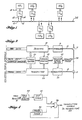
- the data communication system illustrated therein is adapted to provide data communications among a plurality of utilization devices UD i -UD s .
- the utilization devices UD 1 -UD may comprise a plurality of avionic systems, or subsystems, or, a plurality of computer-related devices such as a central processing unit (CPU), input/output (I/O) devices, displays, memories, or the like.
- Each of the utilization devices UD 1 -UD may include means for transmitting data, means for receiving data, or both.
- utilization devices UD 1 -UD are capable of transmitting and receiving data
- utilization device UD 5 is capable only of receiving data.
- the data communication system of the present invention includes a plurality of terminals TL 1 ⁇ TL 5 which are associated with respective ones of the utilization devices UD 1 -UD . , and also includes a common data communication medium to which the plurality of terminals TL i- TL 5 are coupled.
- the data communication medium comprises a data bus DB, which may take many forms, such as one or more electrical conductors, a magnetic members, a waveguide, or a fiber- optic member.
- the data bus DB includes a single twisted pair of wires extending to the physical locations of the utilization devices UD 1 -UD . .
- the present invention does not require, however, that the data communication medium be limited to a physical apparatus such as data bus DB, so that the data communication medium may comprise any appropriate carrier, such as audio, radio or light frequency waves or pulses, which is capable of carrying information by way of modulation thereof.
- the data communication medium may comprise any appropriate carrier, such as audio, radio or light frequency waves or pulses, which is capable of carrying information by way of modulation thereof.
- each-terminal includes a data communications link 10 for exchanging data with its associated utilization device, an output 12 upon which transmitted data appears and which is coupled to the data bus DB by a bus coupler 13, and an input 14 for receiving data present on the data bus DB, with the input 14 being coupled to the data bus DB by a bus coupler 15.
- the data to be transmitted and received using the data bus DB is in the form of messages comprising one or more, successive serial digital words.
- each terminal includes a demodulator 16 for demodulating the messages on the data bus DB received via coupler 15 and input 14 and for supplying the demodulated messages to a receiver 18.
- the demodulated messages are temporarily stored within the receiver 18, and the data therein is sent in an appropriate format to the associated utilization device under control of a terminal control unit 20 which exchanges "interface handshake" information with the utilization device and which provides the utilization device with an identification of the data and that has been received.
- a transmitter 22 receives data from its associated utilization device, again under control of the terminal control unit 20 and outputs such data in the form of messages comprising one or more successive, digital words at periodic transmission intervals determined by the terminal control unit 20.
- a modulator 24 modulates the messages in a desired manner and supplies the modulated messages to the data bus DB via the output 12 and bus coupler 13.
- the terminal control units 20 in the plurality of terminals TL i -TL 4 utilize an identical and unique terminal control routine, or protocol, which insures that only one terminal is transmitting at a given time and that, under steady-state conditions, transmission by any terminal occurs at periodic transmission intervals.
- the protocol requires that: (a) the transmission interval for each terminal be the nominal time interval between the initiation of periodic data transmissions by the terminal, and that the transmission intervals for all terminals be approximately the same in duration; (b) each transmitting terminal be capable of transmitting one message, including one or more data words, with appropriate labels, check words and parity words during each transmission interval; (c) each message can have any desired duration so long as such duration is fixed during times when periodic transmission by the terminal is required and so long as the sum of the durations of the messages of all terminals, and all inter-message gaps, plus a growth gap to be described hereinafter, does not exceed the duration of each transmission interval; (d) each transmitting terminal initiates data transmission only upon the concurrence of the expiration of an inter-message gap on the data bus which is unique to that transmitting terminal, and, the elapse of a period of time, from a previous transmission by the terminal, which is substantially equal to the transmission interval; and, (e) any inter-word gaps in any message have a duration which is
- a transmission interval timer 30 is reset at the time of a previous message transmission by the terminal, as explained hereinafter, and provides an output signal at elapse of a predetermined period of time thereafter, the predetermined period being substantially equal to the transmission interval.
- a word gap detector 32 receives the demodulated messages from the receiver 18 and provides an output signal only when such demodulated messages are absent, signifying an inter-word or inter-message gap on the data bus DB.
- a gap timer 34 is adapted to time the duration of each output signal from the word gap detector 32 and to provide an output signal only when the duration of the output signal from word gap detector 32 exceeds the unique inter-message gap assigned to the terminal.
- An AND gate 36 provides a transmitter enable signal to the transmitter 22 only upon concurrence of the output signals from transmission interval timer 30 and gap timer 34, so that transmitter 22 is enabled to transmit a message on the data bus DB.
- the resultant transmission of a message causes word gap detector 32 to terminate its output signal, thereby resetting gap timer 34, and the transmitter enable signal is used to reset transmission interval timer 30, so that the terminal control unit 20 is again enabled to detect the conditions that will permit a subsequent message transmission by the terminal.
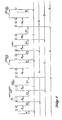
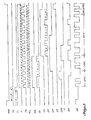
- Figure 3 comprises a timing chart illustrating a plurality of successive cycles of operation of the data communication system under ideal, steady-state conditions.
- Terminals TL 1 ⁇ TL 4 are capable of transmitting messages, with the message being transmitted by each of the terminals TL 1 ⁇ TL 3 including two successive data words, each data word being of a predetermined length and being preceded by a label identifying the data therein, and with the data words in each message being separated by an inter-word gap.
- the messages M 11 , M 21 and M 3 , transmitted by the terminals TL 1 ⁇ TL 3 during the first illustrated cycle of operation of the data communication system are of equal duration.
- the message M 41 of terminal TL 4 includes three data words, each data word being of a predetermined length and being preceded by a label identifying the data therein, the data words again being separated by an inter-word gap and with message M 41 therefore being longer in duration than messages M 11 , M 21 and M 31 .
- terminals TL 1 ⁇ TL 3 transmit messages M 12 , M 22 and M 32 , each of identical duration to corresponding messages M 11 , M 21 and M 31 , and terminal TL 4 transmits message M 42 of identical duration to message M 41 .
- the terminal control unit 20 in each of the terminals TL 1 ⁇ TL 4 establishes (through its gap timer 34) a unique inter-message gap for the associated terminal (that is, gaps g 1 , g 2 , g 3 and g 4 for terminals TL 1 , TL 2 , TL 3 and TL 4 , respectively, with g 1 ⁇ g 2 ⁇ g 3 ⁇ g 4 ).
- the terminal control unit 20 in each of the terminals TL 1 ⁇ TL 4 also establishes a transmission interval through its transmission interval timer 30 (that is, transmission intervals T 1 , T 2 , T 3 and T 4 for terminals TL 1 , TL 2 , TL 3 and TL 4 , respectively, with T 1 ⁇ T 2 ⁇ T 3 ⁇ T 4 ).
- the transmitter 22 in each of the terminals TL 1 ⁇ TL 4 is not enabled until concurrence of expiration of the unique inter-message gap associated with the terminal and elapse of the transmission interval for that terminal.
- transmitter 22 in terminal TL is transmitting message M 11 , during its associated transmission interval T 1 , and that the transmission intervals T 2 ⁇ T 4 have not yet elapsed.
- the absence of messages on the data bus DB causes the gap times 34 in each of the terminals TL 1 ⁇ TL 4 to begin timing.
- the gap timer 34 in terminal TL provides an output signal.
- no transmitter enable signal is provided by AND gate 36 in terminal TL 1 , and accordingly transmitter 22 therein is not enabled.
- the gap timer 34 in terminal TL 2 provides an output signal upon expiration of the gap g 2 associated therewith.
- the transmission interval T 2 for terminal TL 2 will also have elapsed, so that a transmitter enable signal is provided by the AND gate 36 in terminal TL 2 to enable the transmitter 22 therein, whereby the message M 21 is transmitted.
- the gap timers 34 in the terminals TL i and TL 3 ⁇ TL 4 are again enabled.
- the inter-word gap is shorter than any of the inter-message gaps (the shortest of which is gap g,)
- the initiation of transmission of the second data word in message M 21 occurs before any of the gap timers 34 provides an output signal, thereby inhibiting the terminals TL 1 , TL 3 and TL 4 from transmission during message M 21 .
- the gap timers 34 in each of the terminals TL 1 ⁇ TL 4 are again enabled.
- the gap timers 34 in terminals TL, and TL 2 again provide an output signal.
- the transmitters 22 in terminals TL i and TL 2 are not enabled inasmuch as their respective transmission intervals T,, T 2 have not again elapsed.
- the gap timer 34 in terminal TL 3 provides an output signal. Since the transmission interval T 3 associated with terminal TL 3 has also elapsed, a transmitter enable signal is provided by AND gate 36 in terminal TL, to enable transmitter 22 therein so that message M 31 is transmitted. Similarly, upon termination of message M 31 , and after expiration of gap g 4 , transmitter 22 in terminal TL 4 is enabled to transmit message M 41 .
- the gap timers 34 in each of the terminals TL 1 ⁇ TL 4 are again enabled.
- the .length of each transmission interval T,-T 4 is chosen to be somewhat longer than the duration of all messages during each cycle of operation of the data communication system (e.g., M 11 +M 21 +M 31 +M 41 ) and the sum of all inter- message gaps (e.g., g,+g2+g3+g4).
- at least the gap timer 34 associated with the terminal having the shortest inter-message gap e.g., gap g, associated with terminal TL, provides an output signal before the first-in- time transmission interval (e.g., interval T 1 ) again elapses.
- the transmitter 22 in terminal TL 1 is next enabled to transmit the message M 12 , whereupon a second cycle of the data communication system is initiated. Operation of the data communication system then proceeds in a manner identical to that previously described for the first cycle of operation thereof, with the successive transmission of messages M 22 , M 32 and M 42 upon expiration of the gaps g 2 , g 3 and g 4 and the elapse of the transmission intervals T 2 , T 3 and T 4 respectively associated with terminals TL 2 , TL 3 and TL 4 .
- the transmission interval timers 30 be synchronized with each other, it is necessary that all transmission intervals be approximately equal in duration so that a successive transmission interval (e.g., T 2 ) does not elapse at or before the elapse of a previous transmission interval (e.g., T,).
- a successive transmission interval e.g., T 2
- a previous transmission interval e.g., T,
- the gap timers 34 be synchronized, it is necessary that they have a stable time base so that the gap of any terminal does not approximate the gap of any other terminal.
- the time base establishing the inter-word gap in each of the terminal control units 20 must be stable so that the inter-word gap of any terminal does not equal or exceed the inter- message gap of any terminal.
- each terminal includes a terminal monitor 40 ( Figure 2) which receives signals from the receiver 18, the terminal control unit 20, and the transmitter 22 therein.
- Each terminal monitor 40 includes an independent time base which establishes the directed inter-word gap, inter-message gap, and transmission interval for its associated terminal.
- the terminal monitor 40 also includes circuitry for comparing the actual inter-word gap, inter- message gap, and transmission interval provided by its associated terminal with the desired inter-word gap, inter-message gap, and transmission interval established by the independent time base therein. If any of these comparisons fail to be made, the terminal monitor 40 supplies a signal to a modulator enable switch 42 which responsively removes power from the modulator 24 to inhibit further transmissions by the associated terminal.
- terminal TL 2 initiates transmission of a message on the data bus DB and initiates its transmission interval T 2 .
- terminals TL i and TL 3 successively engage in transmissions upon the data bus DB, and initiate their respective transmission intervals T,, T 3 .
- a cycle of operation of the data communication system will consist of successive transmissions from terminals TL 4 , TL 2 , TL, and TL 3 , with simultaneous transmission by two or more terminals being inhibited by the protocol which requires concurrence of the expiration of the unique inter-message gap and the elapse of the transmission interval associated with each terminal.
- the "growth gap”, or the time between the termination of the last message in the cycle of operation of the data communication system and the initiation of a successive cycle of operation thereof, always precedes the transmission interval of the terminal having the slowest time base, that is, the terminal whose transmission interval timer 30 has the longest actual period.
- the transmission interval timer 30 in terminal TL 4 has the longest actual period.
- the timer at which a message transmitted by terminal TL 4 occurs is successively delayed in successive cycles of operation of the data communication system, with the result that the growth gap illustrated in Figure 3 becomes successively shorter, until the growth gap is reduced to the inter-message gap g, associated with terminal TL,.
- the gap between termination of each message transmission by terminal TL 3 and the initiation of each message transmission by terminal TL 4 successively increases until it reaches a duration equal to the duration of the growth gap illustrated in Figure 3.
- the periodicity of each cycle of operation of the data communication system will be determined by that one of the terminals TL,-TL 4 having the slowest transmission interval timer 30.
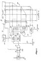
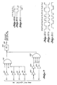
- the data bus DB comprises a twisted pair of wires 100 extending to all terminals, with the terminations (not illustrated) of the twisted pair of wires 100 being short-circuited so that the data bus DB comprises a single, continuous current loop.
- Messages on the data bus DB are in the form of currents, and are coupled to and from each transmitting terminal by an associated bus coupler 102 which includes a core 104 whose legs are inserted into two adjacent loops formed by the twisted pair of wires 100 so that each wire thereof constitutes a single turn of a primary winding of the bus coupler 102.
- a secondary winding 106 is also wound around the core 104 and is interconnected with the transmitting terminal by a terminal stub 108 comprising a twisted pair of wires.
- the terminal stub 108 is connected in common to the input of a demodulator 110 and to the output of a modulator 112.
- the output from demodulator 110 comprises a signal DMR which represents the demodulated message and which is applied to the input of a receiver 114 whose construction and operation will be described hereinafter with reference to Figure 6.
- the outputs from receiver 114 comprise a signal ADA, which is produced upon the absence of messages upon the data bus DB, and a plurality of parallel, binary output signals DR, which represent the data within any message on the data bus DB and received by the receiver 114.
- An interface unit 116 is provided for controlling the interchange of data between the terminal and its associated utilization device 118.
- a latch circuit 120 to which is applied the parallel, binary output signals DR from receiver 114 and which is operative to store the received data represented by such signals DR under control of signal LD from receiver 114 as described hereinafter.
- the received data in latch 120 is converted into an analog signal by a D/A converter 122, amplified by an amplifier 124, and supplied to the utilization device 118.
- the utilization device 118 provides an analog output signal, representing the data to be transmitted, to interface unit 116.
- the analog output signal from utilization device 118 is amplified by an amplifier 126, converted into a parallel, digital format by an A/D converter 128, and stored in a shift register 130.
- the transmitted data within shift register 130 is transferred as a signal DT, in serial, digital form, to transmitter 132.
- transmitter 132 At periodic transmission intervals in accordance with the above-described protocol, and in response to the signal ADA from receiver 114, transmitter 132 provides an output signal DM, in serial digital form, representing the transmitted data, the label or address of the terminal, and synchronizing and parity information.
- the signals DM and T from the transmitter 132 are applied to modulator 112 whose output has three distinct states. During the time that the signal T is absent, the output of modulator 112 has a high impedance so as to decouple the modulator 112 from the data bus DB.
- the output of modulator 112 has present thereon an output signal which alternates between first and second levels in response to the signal DM, with the first and second levels being respectively positive and negative.
- the output signal from modulator 112 is applied directly to the input of demodulator 110, and via terminal stub 108 and bus coupler 102 to the data bus DB.
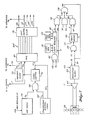
- each message comprises a serial digital word having, in sequential order, a three-bit SYNC word, a three-bit LABEL word, an eight-bit DATA word, a PAD bit, and a PARITY bit.
- the format of each message transmitted is Manchester bi-phase level modulation, wherein successive positive and negative levels in the output signal from modulator 112 represent a "1" and successive negative and positive levels in the output signal from modulator 112 represent a "0".
- the demodulator 110 includes an amplifier 140 which provides a POS output for the duration of each positive level of the signal on data bus DB, and which provides an NEG output for the duration of each negative level of the signal on the data bus DB.
- sense amplifier 140 provides no output.
- the POS and NEG outputs of sense amplifier 140 are applied to respective inputs of an OR gate 142 whose output comprises the signal ADA.
- the signal ADA when either the POS or NEG outputs are being provided by sense amplifier 140, the signal ADA is at a higher logic level, signifying the presence of a message on the data bus DB.
- the signal ADA switches to a low logic level, signifying the absence of any message on the data bus DB.
- Gap timer 150 may comprise a monostable multivibrator which is adapted to provide a momentary output signal TG at a predetermined time after each high level-low level transition in the signal ADA, with the predetermined time corresponding to the desired inter- message gap g 1 .
- Transmitter 132 also includes a transmission interval timer 152, which also may comprise a monostable multivibrator, and which is adapted to provide a momentary output signal T1 at a predetermined time after the application of a signal ST1 thereto.
- signal ST1 is provided at the end of a message transmission from the terminal, and the predetermined time of transmission interval timer152 is chosen so that the signal T1 is provided at a time corresponding to the desired transmission interval T 1 for the terminal.
- Signals TG and T1 are applied to respective inputs of an AND gate 154 whose output is connected to the input of a clock control circuit 156, which may comprise a resettable RS flip-flop.
- a clock control circuit 156 which may comprise a resettable RS flip-flop.
- AND gate 154 provides an output signal which sets clock control circuit 156 into a first state thereof, wherein an output signal T thereof goes to a high logic level to initiate a message transmission from the terminal.
- the signal T is applied to a transmit clock 158, a program counter 160, a shift register 162, a line driver 164, and a parity generator 184 in transmitter 132, as well as to the shift register 130 in interface unit 116, to control the operation of those components as described hereinafter.
- transmit clock 158 is enabled to produce clock signals TS and TCL ( Figure 8), with the frequency of the signal TCL being twice that of the signal TS.
- the clock signal TCL is applied to the program counter 160.
- the clock signal TS is applied to a modulation matrix circuit 168, an AND gate 166, and an AND gate, 182 in transmitter 132, as well as to the shift register 130 in interface unit 116.
- the program counter 160 which may comprise a fixed-length, binary counter, provides a plurality of binary output signals 160A to a transmit control ROM 170 which is appropriately programmed to respond to the binary output signals 160A to provide signals XSL, XD, CP, XP and XS2 which have a high logic level during a desired transmission of the SYNC word and LABEL word, a desired transmission of the DATA, a desired parity check, a desired transmission of the PARITY bit, and a desired modification of the SYNC word, respectively. More specifically ( Figure 8), XSL goes to a high logic level at the time signal T goes to a high logic level, and goes to a low logic level upon the initiation of the thirteenth pulse in the clock signal TCL.
- XD goes to a high logic level upon the initiation of the thirteenth pulse in clock signal TCL, and goes to a low logic level at the initiation of the thirty-first pulse in the clock signal TCL.
- CP goes to a high logic level at the initiation of the seventh pulse in the clock signal TCL, and goes to a low logic level at the initiation of the twenty-first pulse in the clock signal TCL.
- XP goes to a high logic level at the initiation of the thirty-first pulse in the clock signal TCL, and goes to a low logic level at the time the signal T goes to a low logic level.
- XS2 goes to a high logic level at the initiation of the fourth pulse in the clock signal TCL, and goes to a low logic level at the initiation of the seventh pulse in the clock signal TCL.
- the three-bit SYNC word and the three-bit LABEL word are stored, respectively, in a SYNC pattern generator 172 and a LABEL generator 174 whose outputs are coupled to respective inputs of shift register 162.
- the SYNC word and the LABEL word are transferred into shift register 162. Since the signal XSL is at a high logic level at this time, AND gate 166 applies the clock signal TS to the clock input of shift register 162 to that the SYNC word and LABEL word are strobed out of shift register 162 to form the signal SL.
- the SYNC word is represented by binary "1 10" and the LABEL word, for terminal TL1, is represented by binary "001 ".
- the signals SL and XSL are applied to respective inputs of an AND gate 176, whereby the signal SL is gated to a first input of an OR gate 178.
- the output signal from OR gate 178 comprises the signal DM which is applied to the modulator 112, and, more specifically, to the modulation matrix circuit 168 therein. Therefore, from the initiation of message transmission to the time that the signal XSL goes to a low logic level, the signal DM comprises the signal SL, as illustrated in Figure 8.
- the LABEL word will of course vary from terminal to terminal. It will also be recognized that the LABEL can identify not only a specific terminal, but also a specific message from that terminal, in which case the LABEL may comprise part of the data to be transmitted by the terminal.
- the signal XD When the signal XSL goes to a low logic level, the signal XD goes to a high logic level. When signal XD goes to a high logic level, shift register 130 is enabled, and the contents thereof are strobed by the signal TS to form the output signal DT.
- the transmitted data is represented by binary "10100010" plus a binary "0" PAD bit which is provided for expansion of such transmitted data.
- the signals XD and DT are applied to respective inputs of an AND gate 180 whose output is coupled to a second input of OR gate 168. Accordingly, the signal DM comprises the signal DT, for the duration of the signal XD, as illustrated in Figure 8.
- the signals DM and TS are applied to respective inputs of an AND gate 182 whose output is coupled to the input of parity generator 184.
- the output of parity generator 184 is a signal P, representing the PARITY bit, and is applied along with the signal XP to respective inputs of an AND gate 186 whose output is coupled to a third input of OR gate 178.
- Parity generator 184 is also provided with the signals T and CP, and may comprise a J-K flip-flop. When the signal T goes to a high logic level at the initiation of message transmission, parity generator 184 is set to a state whereupon the output signal P thereof is at a low logic level.
- parity generator 184 is enabled and is responsive to low-high logic level transitions in the signal DM, as strobed through AND gate 182 by clock signal TS, to toggle its output signal P between low and high logic levels.
- the signal P goes to a high logic level upon the first low-high logic level transition in the signal DM, and then goes to a low logic level at the next low-high logic level transition in the signal DM.
- the signal CP returns to a low logic level
- the signal P remains at a low logic level and is gated through AND gate 186 at the time that the signal XP goes to a high logic level.
- the signal DM comprises the signal P, for the duration of the signal XP, as illustrated in Figure 8.
- the signal DM is applied to the modulation matrix circuit 168 which responds to the clock signal TS to develop a Manchester bi-phase level modulated output signal DB therefrom.
- modulation matrix circuit 168 The operation of modulation matrix circuit 168 is largely conventional. However, the last bit of the SYNC word is "zero", which would normally result in a low-high logic level transition in the output signal DB. To insure the proper operation of the receivers in the participating terminals of the data communication system, the signal XS2 causes the modulation matrix circuit 168 to maintain the output signal DB at a low logic level during the time occurrence of the third bit in the SYNC word, as best seen in Figure 8.
- the output signal from modulation matrix circuit 168 is applied to the input of the line driver 164.
- the output from line driver 164 is at a high impedance.
- line driver 164 converts each high logic level of the output signal from modulation matrix circuit 168 into a corresponding positive level, and each low logic level of the output signal from a modulation matrix circuit 168 into a corresponding negative level.
- program counter 160 At the time that the count in program counter 160 has advanced to its maximum value, program counter 160 provides signal ST1 which resets clock control circuit 156 into a second state. As a result, the signal T goes to a low logic level to terminate the message transmission by resetting program counter 160, clearing shift register 162, clearing shift register 130 in interface unit 116, and returning line driver 164 to a high impedance state. Simultaneously, signal ST1 re-initiates the timing period of transmission interval timer 152. The transmission interval T1 from the terminal TL 1 is accordingly determined by the duration of the message transmission for the terminal, which is of fixed duration, plus the time period established by transmission interval timer 152. Accordingly, even though the gap timer 150 will subsequently provide one or more signals TG, a subsequent message transmission from terminal TL,, cannot occur until the elapse of the transmission interval T 1 as determined by the signal T1 from transmission interval timer 152.
- the signal ADA in the receiver 114 is applied to the input of a clock control circuit 190 and to the input of a word gap detection circuit 192.
- the clock control circuit 190 may comprise an R/S flip-flop, and the word gap detection circuit 192 may comprise a monostable multivibrator.
- the clock control circuit 190 is set to a first state in which an output signal R therefrom has a high logic level.
- the signal R is applied to a receiver clock 194 which is operative to provide a clock signal RCL whenever the signal R has a high logic level.
- a shift register 196 is provided for storing messages, as coupled thereto by the POS output of sense amplifier 140 and under control of the clock signal RCL. Therefore, when a message appears on the data bus DB, the signal R goes to a high level, the clock signal RCL is produced, and the message is sequentially transferred into the shift register 196.
- outputs "1 "-"6" of the shift register 196 representing the bit locations of the SYNC word, are coupled to respective inputs of sync pattern detection circuit 200.
- Outputs "7"- "20” of the shift register 196, representing the message bits used for generation of the PARITY bit, and outputs "31"-"32" of the shift register 196, representing the bit locations of the PARITY bit are coupled to respective inputs of parity checker circuit 202.
- Outputs "7"- "12” of the shift register 196 representing the bit locations of the LABEL word, are applied to respective inputs of the label decoder 204.
- Sync pattern detection circuit 200 may comprise a decoder whose output signal SPD goes to a high logic level when the signals applied to its input represent the desired SYNC word.
- the signal SPD is applied to a second input of clock control circuit 190, and to an AND gate 206.
- the parity checker circuit 202 includes a decoder which is operative to provide a signal representing the binary state of the desired PARITY bit as developed from the message bits used to develop that PARITY bit, and a comparator which is operative to provide an output signal GP which has a high logic level when the value of the desired PARITY bit is equal to that of the actual PARITY bit.
- AND gate 206 provides an output signal OE which is applied to an ENABLE input of label decoder 204.
- shift register 196 As the message on the data bus DB is transferred into the shift register 196, the presence of the proper SYNC word in the appropriate storage locations of shift register 196 causes the output signal SPD from sync pattern detection circuit 200 to go to a high logic level.
- signal SPD goes to a high level
- clock control circuit 190 is reset to a second state, whereupon signal R therefrom goes to a low level, thereby terminating the signal RCL from receiver clock 194 and accordingly terminating the transfer of the message into shift register 196.
- the sync pattern detection circuit 200 includes an AND gate 218 whose output is coupled to the input of a monostable multivibrator 220 which is capable of providing the output signal SPD.
- the "1" output of shift register 196 (as routed through matrix circuit 198) is coupled directly to a first input of AND gate 218; the "2" output of shift register 196 is coupled through an inverter 210 to a second input of AND gate 218; the “3” output of shift register 196 is coupled directly to a third input of AND gate 218; and, the "4", "5" and “6” outputs of shift register 196 are coupled through respective inverters 212, 214 and 216 to a fourth input of AND gate 218.
- the SYNC word precedes the remainder of the message and is represented in the message by a positive bit level, a negative bit level, a positive bit level, and three negative bit levels, in succession.
- the SYNC word therefore has the pattern illustrated in Figure 10(a).
- the parallel, binary output signals DR ( Figure 5) presented to the latch circuit 120, which are those present on the odd-numbered outputs in the group of outputs "13"-"28" of shift register 196 ( Figure 11 (a)), therefore represent "10100010", or, the data that has been transmitted.
- the sync pattern detection circuit 200 includes a second AND gate 228 whose output is coupled to the input of monostable multivibrator 220.
- shift register 196 is coupled through series inverters 222, 224, and the "2" output of shift register 196 is coupled through an inverter 226, to a first input of AND gate 228.
- the "3", "4" and “5" outputs of shift register 196 are coupled directly to respective second, third and fourth inputs of AND gate 228.
- the receiver clock 194 ( Figure 6) remains enabled and the clock signal RCL therefrom continues to transfer the message into and through the shift register 196.
- the pattern of the SYNC word causes AND gate 228 to provide an output signal to cause monostable multivibrator 220 to provide the output signal SPD to terminate the message transfer.
- the embodiment of the sync pattern detection circuit 200 in Figure 9 allows proper decoding of the transmitted data, irrespective of the polarity with which the message has been provided to the receiver 114.
- the pattern of the SYNC word in the message is an improper code for Manchester bi-phase level modulation, that is, the pattern of the SYNC word includes three successive logic levels of a given type, whereas a proper Manchester bi-phase level code permits only two successive logic levels of the same type. Accordingly, messages not have the pattern of the SYNC word do not cause the sync pattern detection circuit 200 to provide its output signal SPD, with the result that such message are transferred through shift register 196 without decoding.
- the signal GP from parity checker circuit 202 will be at a high logic level, so that the signal OE from AND gate 206 is provided to enable label decoder 204.
- An output signal LD is provided by label decoder, however, only if the LABEL word in the message identifies data which the terminal is to receive.
- the signal LD is applied to an enable input of latch circuit 120 in interface unit 116 ( Figure 5).
- the outputs "13"-"28" of shift register 196, on which appear the parallel, binary output signals DR representing the DATA word are connected to respective signal inputs of latch circuit 120. If the LABEL word in the message is correct, the signal LD enables latch circuit 120 so as to transfer the signals DR thereto.
- word gap detection circuit 192 When the signal ADA again goes to a high logic level, signifying the absence of a message on the data bus DB, the word gap detection circuit 192 is enabled. At a predetermined time thereafter, word gap detection circuit 192 provides a signal WGD which clears shift register 196, thereby conditioning the terminal for the reception of a successive message.
- the present invention permits each participating terminal to have autonomous access to the data bus DB.
- the receiver in any one terminal is capable of detecting and storing any messages transmitted on the data bus DB, and to transfer the data within any such message to its associated utilization device upon proper message identification, irrespective of the operation of any other terminal.
- the transmitter in any one terminal can transmit a message on the data bus DB in response only to the absence of messages on the data bus DB, and thus irrespective of the transmission by any other terminal.
- the invention permits periodic transmission of messages by each terminal without the requirement for a central bus controller terminal, and yet avoids the simultaneous transmission of messages by two or more terminals. Further, failure of any terminal or terminals will not constitute failure of any other terminal.
- the failure of a receiver in any one terminal will not affect the operation of the receiver or transmitter in any other terminal.
- the failure of the transmitters in all terminals, except one, to transmit messages will not result in the transmitter in that one terminal failing to periodically transmit its message, inasmuch as message transmission from that one terminal is dependent only upon the expiration of the unique inter- message gap (which in this case will be measured from the termination of the message transmission of that one terminal) and the elapse of the transmission intervals for that one terminal.
- the failure of a demodulator, receiver, transmitter or modulator in any one terminal will not result in failure of the data bus DB, provided that a data bus and associated couplers such as those disclosed herein are used.
- a short circuit across the seondary winding 106 of the bus coupler 102, or a broken core 104 will reduce the inductance of the bus coupler 102 so as to have the same effect upon the operation of the data bus DB as would be caused by removal of the bus coupler 102.
Abstract
Description
- The invention relates to method and apparatus which permits each of a plurality of terminals coupled to a data communication medium of a data communication system to autonomously and periodically transmit messages on said data communication medium, comprising the steps, at each said terminal, of: detecting the absence of messages on said data communication medium, and enabling transmission of a message by said terminal only upon the occurrence of an absence of messages on said data communication medium.
- Such a method is known from DE-A-2 442 736.
- In modern aircraft, it is desirable to integrate, as far as possible, the functions of previously-independent avionic systems to permit an attendant reduction in weight, space and power requirements of the avionic systems and a simplification in wiring between physically separated avionic systems or subsystems thereof. Such integration has been achieved by the use of a common data communication medium, or data bus, to which each avionic systems, or subsystem thereof, has access through an associated terminal, each of which is capable of transmitting and receiving data on the data bus. Data transmitted on the data bus by one terminal associated with a particular system or subsystem can be received by the terminals associated with the remaining systems or subsystems, thus eliminating the requirement for separate wiring interconnections between the systems or subsystems. In addition, data generated in a particular system or subsystem can be used by any other system or subsystem without the necessity of having to independently generate that data.
- In order for a data communication system using a data bus to properly and reliably operate, without degradation upon the performance of any of the systems or subsystems coupled thereto, it is desirable that the data communication system allow transmission of data originating from any terminal to any or all of the remaining terminals using a minimum physical length of the data bus. Also, the data communication system must be capable of accommodating periodic transmission of any or all data. For example, if a particular terminal is inhibited from transmitting in a periodic manner, then those terminals that depend upon such data may malfunction. Further, operation of any one of the systems, subsystems or terminals associated therewith, must not be affected by the operational status of any other system, subsystem or terminal, whether such other system, subsystem or terminal be operating normally or be malfunctioning. Finally, the data bus, and any devices for coupling the data bus to each terminal which conceivably could render the data bus unusable, must be of such high functional integrity so as to make the possibility of data bus failure extremely remote.
- The data communication systems using a data bus that have been particularly proposed for use in aircraft have taken two forms. The first, known as a broadcast bus, includes a single data bus which is exclusively assigned to one data source terminal. Data transmitted on the data bus from the data source terminal can be received by any number of receiver terminals coupled to the data bus. Although the broadcast bus is capable of accommodating periodic data transmissions, it is not capable of bilateral data communications. Accordingly, a separate data bus must be used for each data source terminal. Also, any device requiring the use of data from more than one data source terminal must be separately coupled with each required data bus. Accordingly, the broadcast bus does not permit a significant reduction to be made in aircraft wiring interconnections.
- The second, known as a multiplex bus using a central bus controller, includes a single data bus having coupled thereto a plurality of remote terminals and a central bus controller terminal. The bus controller terminal determines (under software control) the mode of operation of any remote terminal, and controls such mode of operation by the transmission of command words on the bus. The multiplex bus, although capable of significantly reducing aircraft wiring interconnections, is not inherently suitable for periodic data transmission by each remote terminal. More important, the operation of remote terminals is not autonomous due to their dependence on the bus controller terminal, so that failure of the bus controller terminal constitutes failure of all remote terminals associated with the data bus.
- Yet another approach used in data communication systems is that taught in French Patent 2,337,477, West German Patent 2,442,736, and in Christensen et al., "Design Analysis of the Access Protocol for Hyper- channel Networks", 3rd U.S.A.-Japan Computer Conference, 1978. In this approach, each transmitting terminal is assigned a unique timing period or "terminal gap". Upon the absence of messages on the data bus, a timer in each terminal is started so that each terminal may time the duration of the absence of messages. When the shortest terminal gap expires, the corresponding terminal transmits a message on the data bus if that terminal is operative and is ready to transmit a message, and this message transmission resets the timers in all other terminals so as to inhibit the transmission of messages thereby. If the terminal having the shortest terminal gap is not operative or is not ready to transmit a message, however, the timers in the remaining terminals continue to run. Upon expiration of the next-longest terminal gap, the corresponding terminal transmits a message if that terminal is operative and is ready to transmit a message, and the timers in the remaining terminals are reset. If that terminal is not operative or is not ready to transmit a message, however, the timers in the remaining terminals continue to run and the process just described is repeated.
- Although this approach is advantageous in that no central bus controller terminal is required to regulate access to the data bus by the various transmitting terminals, it is inherently incapable of permitting any terminal (excepting perhaps the terminal having the shortest terminal gap) to engage in periodic transmissions on the data bus. As an illustration of this point, let it be assumed that the terminal having the shortest terminal gap is always operative and is always ready to transmit messages on the data bus. In such a situation, the remaining terminals will be precluded from access to the data bus for the purpose of message transmissions thereon since the shortest terminal gap will always expire before the expiration of the longer terminal gaps associated with the remaining terminals. Therefore, the remaining terminals will not only be precluded from periodic message transmissions but also from any message transmissions on the data bus.
- It is therefore an object of this invention to provide an improved data communication system using a data bus.
- It is a further object of this invention to provide such a data communication system which permits each participating terminal to have automonous access to the data bus.
- It is yet a further object of this invention to provide such a data communication system in which normal operation of any participating terminal, or malfunction thereof, will not affect the operation of the data communication system or of any other participating terminal associated therewith.
- It is another object of this invention to provide such a data communication system which permits each participating terminal to engage in periodic data transmissions on the data bus.
- It is yet another object of this invention to provide such a data communication system which affords multiplexed data communications among participating terminals without the requirement for a central bus controller terminal.
- It is still another object of this invention to provide such a data communication system which permits a significant reduction in the wiring requirements between participating systems and a significant increase in the integration of such systems.
- The foregoing objects, and other objects and advantages that will be apparent to those of ordinary skill in the art, are achieved by the use of a method which permits a plurality of terminals to autonomously and periodically transmit messages on a data communication medium. At each terminal, the absence of messages on the data communication medium is detected. Transmission of a message by each terminal is enabled, however, only upon the occurrence of an absence of messages on the data communication medium whose duration substantially equals that of an inter-message gap unique to that terminal, and, the elapse of a transmission interval from a previous transmission of a message by that terminal. The duration of the transmission intervals of all terminals is substantially the same and is chosen to be greater than the sum of all terminal inter- message gaps and of the durations of all messages transmitted by the terminals since a previous transmission of a message by each terminal.
- The invention can best be understood by reference to the following portion of the specification, taken in conjunction with the accompanying drawings, in which:
- Figure 1 is a block diagram of the data communication system using a data bus and having a plurality of participating terminals coupled thereto;
- Figure 2 is a block diagram of a tpyical participating terminal;
- Figure 3 is a timing diagram illustrating the operation of the data communication system under ideal, steady-state conditions;
- Figure 4 is a block diagram of a portion of a terminal control unit in Figure 2;
- Figure 5 is a block diagram of a simplified version of a participating terminal, and of an associated utilization device and interface unit;
- Figure 6 is a block diagram of a demodulator and a receiver in Figure 5;
- Figure 7 is a block diagram of a transmitter and a modulator in Figure 5;
- Figure 8 is a timing diagram illustrating the operation of the transmitter and modulator in Figure 7;
- Figure 9 is a block diagram of a sync pattern detection circuit in Figure 6; and,
- Figures 10 and 11 are signal diagrams illustrating the operation of the sync pattern detection circuit in Figure 9.
- With reference now to Figure 1, the data communication system illustrated therein is adapted to provide data communications among a plurality of utilization devices UDi-UDs. In practical applications, the utilization devices UD1-UD, may comprise a plurality of avionic systems, or subsystems, or, a plurality of computer-related devices such as a central processing unit (CPU), input/output (I/O) devices, displays, memories, or the like. Each of the utilization devices UD1-UD, may include means for transmitting data, means for receiving data, or both. In Figure 1, utilization devices UD1-UD, are capable of transmitting and receiving data, whereas utilization device UD5 is capable only of receiving data. The data communication system of the present invention includes a plurality of terminals TL1―TL5 which are associated with respective ones of the utilization devices UD1-UD., and also includes a common data communication medium to which the plurality of terminals TLi-TL5 are coupled. In the embodiment shown in Figure 1 and discussed hereinafter, the data communication medium comprises a data bus DB, which may take many forms, such as one or more electrical conductors, a magnetic members, a waveguide, or a fiber- optic member. Preferably, the data bus DB includes a single twisted pair of wires extending to the physical locations of the utilization devices UD1-UD.. The present invention does not require, however, that the data communication medium be limited to a physical apparatus such as data bus DB, so that the data communication medium may comprise any appropriate carrier, such as audio, radio or light frequency waves or pulses, which is capable of carrying information by way of modulation thereof.
- In Figure 1, each-terminal includes a data communications link 10 for exchanging data with its associated utilization device, an
output 12 upon which transmitted data appears and which is coupled to the data bus DB by abus coupler 13, and aninput 14 for receiving data present on the data bus DB, with theinput 14 being coupled to the data bus DB by abus coupler 15. In the embodiment shown in Figure 1 and discussed hereinafter, the data to be transmitted and received using the data bus DB is in the form of messages comprising one or more, successive serial digital words. - Referring now to Figure 2, each terminal includes a
demodulator 16 for demodulating the messages on the data bus DB received viacoupler 15 andinput 14 and for supplying the demodulated messages to areceiver 18. The demodulated messages are temporarily stored within thereceiver 18, and the data therein is sent in an appropriate format to the associated utilization device under control of aterminal control unit 20 which exchanges "interface handshake" information with the utilization device and which provides the utilization device with an identification of the data and that has been received. Atransmitter 22 receives data from its associated utilization device, again under control of theterminal control unit 20 and outputs such data in the form of messages comprising one or more successive, digital words at periodic transmission intervals determined by theterminal control unit 20. Amodulator 24 modulates the messages in a desired manner and supplies the modulated messages to the data bus DB via theoutput 12 andbus coupler 13. - Normally, the
receiver 18 in each terminal is enabled and thetransmitter 22 is disabled. Theterminal control units 20 in the plurality of terminals TLi-TL4 utilize an identical and unique terminal control routine, or protocol, which insures that only one terminal is transmitting at a given time and that, under steady-state conditions, transmission by any terminal occurs at periodic transmission intervals. - In detail, the protocol requires that: (a) the transmission interval for each terminal be the nominal time interval between the initiation of periodic data transmissions by the terminal, and that the transmission intervals for all terminals be approximately the same in duration; (b) each transmitting terminal be capable of transmitting one message, including one or more data words, with appropriate labels, check words and parity words during each transmission interval; (c) each message can have any desired duration so long as such duration is fixed during times when periodic transmission by the terminal is required and so long as the sum of the durations of the messages of all terminals, and all inter-message gaps, plus a growth gap to be described hereinafter, does not exceed the duration of each transmission interval; (d) each transmitting terminal initiates data transmission only upon the concurrence of the expiration of an inter-message gap on the data bus which is unique to that transmitting terminal, and, the elapse of a period of time, from a previous transmission by the terminal, which is substantially equal to the transmission interval; and, (e) any inter-word gaps in any message have a duration which is less than that of the shortest inter-message gap.
- Requirements (a) and (d) of the protocol must be met in every application of the invention and can be embodied in each
terminal control unit 20 by the use of circuitry such as illustrated in Figure 4. Atransmission interval timer 30 is reset at the time of a previous message transmission by the terminal, as explained hereinafter, and provides an output signal at elapse of a predetermined period of time thereafter, the predetermined period being substantially equal to the transmission interval. Aword gap detector 32 receives the demodulated messages from thereceiver 18 and provides an output signal only when such demodulated messages are absent, signifying an inter-word or inter-message gap on the data bus DB. Agap timer 34 is adapted to time the duration of each output signal from theword gap detector 32 and to provide an output signal only when the duration of the output signal fromword gap detector 32 exceeds the unique inter-message gap assigned to the terminal. An ANDgate 36 provides a transmitter enable signal to thetransmitter 22 only upon concurrence of the output signals fromtransmission interval timer 30 andgap timer 34, so thattransmitter 22 is enabled to transmit a message on the data bus DB. The resultant transmission of a message causesword gap detector 32 to terminate its output signal, thereby resettinggap timer 34, and the transmitter enable signal is used to resettransmission interval timer 30, so that theterminal control unit 20 is again enabled to detect the conditions that will permit a subsequent message transmission by the terminal. - To more fully understand the operation of the data communication system, reference should be made to Figure 3 which comprises a timing chart illustrating a plurality of successive cycles of operation of the data communication system under ideal, steady-state conditions.
- Terminals TL1―TL4 are capable of transmitting messages, with the message being transmitted by each of the terminals TL1―TL3 including two successive data words, each data word being of a predetermined length and being preceded by a label identifying the data therein, and with the data words in each message being separated by an inter-word gap. As illustrated, the messages M11, M21 and M3, transmitted by the terminals TL1―TL3 during the first illustrated cycle of operation of the data communication system are of equal duration. The message M41 of terminal TL4 includes three data words, each data word being of a predetermined length and being preceded by a label identifying the data therein, the data words again being separated by an inter-word gap and with message M41 therefore being longer in duration than messages M11, M21 and M31. During the second cycle of operation of the data communication system illustrated in Figure 3, terminals TL1―TL3 transmit messages M12, M22 and M32, each of identical duration to corresponding messages M11, M21 and M31, and terminal TL4 transmits message M42 of identical duration to message M41.
- The
terminal control unit 20 in each of the terminals TL1―TL4 establishes (through its gap timer 34) a unique inter-message gap for the associated terminal (that is, gaps g1, g2, g3 and g4 for terminals TL1, TL2, TL3 and TL4, respectively, with g1<g2<g3<g4). Theterminal control unit 20 in each of the terminals TL1―TL4 also establishes a transmission interval through its transmission interval timer 30 (that is, transmission intervals T1, T2, T3 and T4 for terminals TL1, TL2, TL3 and TL4, respectively, with T1≃T2≃T3≃T4). As previously indicated, thetransmitter 22 in each of the terminals TL1― TL4 is not enabled until concurrence of expiration of the unique inter-message gap associated with the terminal and elapse of the transmission interval for that terminal. - With reference again to Figure 3, let it be asumed that
transmitter 22 in terminal TL, is transmitting message M11, during its associated transmission interval T1, and that the transmission intervals T2―T4 have not yet elapsed. At the termination of message M11, the absence of messages on the data bus DB causes thegap times 34 in each of the terminals TL1―TL4 to begin timing. After the expiration of a time equal to gap g1, thegap timer 34 in terminal TL, provides an output signal. However, since the transmission interval T1 for terminal TL1 has not yet again elapsed, no transmitter enable signal is provided by ANDgate 36 in terminal TL1, and accordinglytransmitter 22 therein is not enabled. Subsequently, thegap timer 34 in terminal TL2 provides an output signal upon expiration of the gap g2 associated therewith. Under the steady-state operation illustrated in Figure 3, the transmission interval T2 for terminal TL2 will also have elapsed, so that a transmitter enable signal is provided by the ANDgate 36 in terminal TL2 to enable thetransmitter 22 therein, whereby the message M21 is transmitted. - After the transmission of the first data word in message M21, the
gap timers 34 in the terminals TLi and TL3―TL4 are again enabled. However, since the inter-word gap is shorter than any of the inter-message gaps (the shortest of which is gap g,), the initiation of transmission of the second data word in message M21 occurs before any of thegap timers 34 provides an output signal, thereby inhibiting the terminals TL1, TL3 and TL4 from transmission during message M21. At the termination of message M21, thegap timers 34 in each of the terminals TL1―TL4 are again enabled. Upon successive expiration of the gaps g, and g2, thegap timers 34 in terminals TL, and TL2 again provide an output signal. However, thetransmitters 22 in terminals TLi and TL2 are not enabled inasmuch as their respective transmission intervals T,, T2 have not again elapsed. Upon subsequent expiration of the gap g3, thegap timer 34 in terminal TL3 provides an output signal. Since the transmission interval T3 associated with terminal TL3 has also elapsed, a transmitter enable signal is provided by ANDgate 36 in terminal TL, to enabletransmitter 22 therein so that message M31 is transmitted. Similarly, upon termination of message M31, and after expiration of gap g4,transmitter 22 in terminal TL4 is enabled to transmit message M41. - After the termination of message M41, the
gap timers 34 in each of the terminals TL1―TL4 are again enabled. As previously noted, the .length of each transmission interval T,-T4 is chosen to be somewhat longer than the duration of all messages during each cycle of operation of the data communication system (e.g., M11+M21+M31+M41) and the sum of all inter- message gaps (e.g., g,+g2+g3+g4). Accordingly, at least thegap timer 34 associated with the terminal having the shortest inter-message gap (e.g., gap g, associated with terminal TL,) provides an output signal before the first-in- time transmission interval (e.g., interval T1) again elapses. Upon the subsequent elapse of transmission interval T1, thetransmitter 22 in terminal TL1 is next enabled to transmit the message M12, whereupon a second cycle of the data communication system is initiated. Operation of the data communication system then proceeds in a manner identical to that previously described for the first cycle of operation thereof, with the successive transmission of messages M22, M32 and M42 upon expiration of the gaps g2, g3 and g4 and the elapse of the transmission intervals T2, T3 and T4 respectively associated with terminals TL2, TL3 and TL4. - Since the
receivers 18 in each of the terminals TL1―TL5 associated with the data bus DB are continuously enabled it can be seen that the data words on the data bus DB can be detected by any of the participating terminals and transferred, upon proper identification, to their associated utilization device. - In order that only one terminal be in a transmitting mode at any one time, it is essential that the protocol previously discussed be strictly adhered to. Although it is not necessary that the
transmission interval timers 30 be synchronized with each other, it is necessary that all transmission intervals be approximately equal in duration so that a successive transmission interval (e.g., T2) does not elapse at or before the elapse of a previous transmission interval (e.g., T,). Likewise, although it is not necessary that thegap timers 34 be synchronized, it is necessary that they have a stable time base so that the gap of any terminal does not approximate the gap of any other terminal. Finally, the time base establishing the inter-word gap in each of theterminal control units 20 must be stable so that the inter-word gap of any terminal does not equal or exceed the inter- message gap of any terminal. - In order to insure that the protocol is strictly adhered to, each terminal includes a terminal monitor 40 (Figure 2) which receives signals from the
receiver 18, theterminal control unit 20, and thetransmitter 22 therein. Each terminal monitor 40 includes an independent time base which establishes the directed inter-word gap, inter-message gap, and transmission interval for its associated terminal. The terminal monitor 40 also includes circuitry for comparing the actual inter-word gap, inter- message gap, and transmission interval provided by its associated terminal with the desired inter-word gap, inter-message gap, and transmission interval established by the independent time base therein. If any of these comparisons fail to be made, the terminal monitor 40 supplies a signal to a modulator enableswitch 42 which responsively removes power from themodulator 24 to inhibit further transmissions by the associated terminal. - The cycles of operation illustrated in Figure 3 represent an ideal, steady-state situation which will not likely be encountered in actual practice. To give an example, let it be assumed that the data communication system has been inoperative and that power is subsequently applied to terminals TL1―TL5. Since the power supplies in the terminals TL1―TL5 will not all come up to operating specifications at the same time, it can be seen that one of the terminals TL1―TL5 will be capable of transmission before the other terminals. Let it be assumed that terminal TL4 is first capable of transmission, and accordingly initiates transmission of a message therefrom on the data bus DB and initiates its associated transmission interval T4. After termination of the message from terminal TL4, let it be assumed that only terminal TL2 is then capable of transmission. Accordingly, after termination of the inter-message gap g2, terminal TL2 initiates transmission of a message on the data bus DB and initiates its transmission interval T2. Subsequently, let it be assumed that terminals TLi and TL3 successively engage in transmissions upon the data bus DB, and initiate their respective transmission intervals T,, T3. As a result, it can be seen that a cycle of operation of the data communication system will consist of successive transmissions from terminals TL4, TL2, TL, and TL3, with simultaneous transmission by two or more terminals being inhibited by the protocol which requires concurrence of the expiration of the unique inter-message gap and the elapse of the transmission interval associated with each terminal.
- It should also be noted that the "growth gap", or the time between the termination of the last message in the cycle of operation of the data communication system and the initiation of a successive cycle of operation thereof, always precedes the transmission interval of the terminal having the slowest time base, that is, the terminal whose
transmission interval timer 30 has the longest actual period. To understand this point, reference should again be made to Figure 3. Let it be assumed that thetransmission interval timer 30 in terminal TL4 has the longest actual period. Accordingly, the timer at which a message transmitted by terminal TL4 occurs, relative to the time occurrence of the termination of the message transmission from the remaining terminals TL1―TL3, is successively delayed in successive cycles of operation of the data communication system, with the result that the growth gap illustrated in Figure 3 becomes successively shorter, until the growth gap is reduced to the inter-message gap g, associated with terminal TL,. At the same time, the gap between termination of each message transmission by terminal TL3 and the initiation of each message transmission by terminal TL4 successively increases until it reaches a duration equal to the duration of the growth gap illustrated in Figure 3. As a result, the periodicity of each cycle of operation of the data communication system will be determined by that one of the terminals TL,-TL4 having the slowesttransmission interval timer 30. - To further illustrate the operation of the data communication system of the present invention, reference will not be made to the construction and operation of a simplified version of each transmitting terminal TL1―TL4.
- In Figure 5, the data bus DB comprises a twisted pair of
wires 100 extending to all terminals, with the terminations (not illustrated) of the twisted pair ofwires 100 being short-circuited so that the data bus DB comprises a single, continuous current loop. Messages on the data bus DB are in the form of currents, and are coupled to and from each transmitting terminal by an associatedbus coupler 102 which includes a core 104 whose legs are inserted into two adjacent loops formed by the twisted pair ofwires 100 so that each wire thereof constitutes a single turn of a primary winding of thebus coupler 102. A secondary winding 106 is also wound around thecore 104 and is interconnected with the transmitting terminal by aterminal stub 108 comprising a twisted pair of wires. - Within the terminal, the
terminal stub 108 is connected in common to the input of ademodulator 110 and to the output of amodulator 112. The output fromdemodulator 110 comprises a signal DMR which represents the demodulated message and which is applied to the input of areceiver 114 whose construction and operation will be described hereinafter with reference to Figure 6. The outputs fromreceiver 114 comprise a signal ADA, which is produced upon the absence of messages upon the data bus DB, and a plurality of parallel, binary output signals DR, which represent the data within any message on the data bus DB and received by thereceiver 114. Aninterface unit 116 is provided for controlling the interchange of data between the terminal and its associatedutilization device 118. Included in theinterface unit 116 is alatch circuit 120 to which is applied the parallel, binary output signals DR fromreceiver 114 and which is operative to store the received data represented by such signals DR under control of signal LD fromreceiver 114 as described hereinafter. The received data inlatch 120 is converted into an analog signal by a D/A converter 122, amplified by anamplifier 124, and supplied to theutilization device 118. - The
utilization device 118 provides an analog output signal, representing the data to be transmitted, to interfaceunit 116. Withininterface unit 116, the analog output signal fromutilization device 118 is amplified by anamplifier 126, converted into a parallel, digital format by an A/D converter 128, and stored in a shift register 130. Under control of signals T, TS and XD from atransmitter 132 within the terminal, as described hereinafter, the transmitted data within shift register 130 is transferred as a signal DT, in serial, digital form, totransmitter 132. At periodic transmission intervals in accordance with the above-described protocol, and in response to the signal ADA fromreceiver 114,transmitter 132 provides an output signal DM, in serial digital form, representing the transmitted data, the label or address of the terminal, and synchronizing and parity information. The signals DM and T from thetransmitter 132 are applied tomodulator 112 whose output has three distinct states. During the time that the signal T is absent, the output ofmodulator 112 has a high impedance so as to decouple the modulator 112 from the data bus DB. During the time that the signal T is present, signifying the transmission of a message from the terminal, the output ofmodulator 112 has present thereon an output signal which alternates between first and second levels in response to the signal DM, with the first and second levels being respectively positive and negative. The output signal frommodulator 112 is applied directly to the input ofdemodulator 110, and viaterminal stub 108 andbus coupler 102 to the data bus DB. - With reference now to Figure 8, only one message is transmitted by each terminal during its transmission interval. As a particular example, each message comprises a serial digital word having, in sequential order, a three-bit SYNC word, a three-bit LABEL word, an eight-bit DATA word, a PAD bit, and a PARITY bit. The format of each message transmitted is Manchester bi-phase level modulation, wherein successive positive and negative levels in the output signal from
modulator 112 represent a "1" and successive negative and positive levels in the output signal frommodulator 112 represent a "0". - With reference now to Figure 6, the
demodulator 110 includes anamplifier 140 which provides a POS output for the duration of each positive level of the signal on data bus DB, and which provides an NEG output for the duration of each negative level of the signal on the data bus DB. At all other times,sense amplifier 140 provides no output. The POS and NEG outputs ofsense amplifier 140 are applied to respective inputs of anOR gate 142 whose output comprises the signal ADA. As illustrated in Figure 8, when either the POS or NEG outputs are being provided bysense amplifier 140, the signal ADA is at a higher logic level, signifying the presence of a message on the data bus DB. When neither the POS nor the NEG outputs fromsense amplifier 140 are present, the signal ADA switches to a low logic level, signifying the absence of any message on the data bus DB. - Let it be assumed that the terminal under discussion is terminal TL1 (Figure 1), with inter- message gap g1 and transmission interval T1. With reference to Figure 7, the signal ADA is applied to a
gap timer 150 withintransmitter 132.Gap timer 150 may comprise a monostable multivibrator which is adapted to provide a momentary output signal TG at a predetermined time after each high level-low level transition in the signal ADA, with the predetermined time corresponding to the desired inter- message gap g1.Transmitter 132 also includes atransmission interval timer 152, which also may comprise a monostable multivibrator, and which is adapted to provide a momentary output signal T1 at a predetermined time after the application of a signal ST1 thereto. As will be described hereinafter, signal ST1 is provided at the end of a message transmission from the terminal, and the predetermined time of transmission interval timer152 is chosen so that the signal T1 is provided at a time corresponding to the desired transmission interval T1 for the terminal. Signals TG and T1 are applied to respective inputs of an ANDgate 154 whose output is connected to the input of a clock control circuit 156, which may comprise a resettable RS flip-flop. With reference to Figure 8, let it be assumed that message transmission on the data bus DB has terminated. Accordingly, the signal ADA goes to a low logic level. At a time g1 thereafter, and at the elapse of the transmission interval T" signified by the signals TG and T1, respectively, ANDgate 154 provides an output signal which sets clock control circuit 156 into a first state thereof, wherein an output signal T thereof goes to a high logic level to initiate a message transmission from the terminal. The signal T is applied to a transmitclock 158, aprogram counter 160, ashift register 162, aline driver 164, and aparity generator 184 intransmitter 132, as well as to the shift register 130 ininterface unit 116, to control the operation of those components as described hereinafter. - When the signal T goes to a high logic level, transmit
clock 158 is enabled to produce clock signals TS and TCL (Figure 8), with the frequency of the signal TCL being twice that of the signal TS. The clock signal TCL is applied to theprogram counter 160. The clock signal TS is applied to amodulation matrix circuit 168, an ANDgate 166, and an AND gate, 182 intransmitter 132, as well as to the shift register 130 ininterface unit 116. - The
program counter 160, which may comprise a fixed-length, binary counter, provides a plurality ofbinary output signals 160A to a transmitcontrol ROM 170 which is appropriately programmed to respond to thebinary output signals 160A to provide signals XSL, XD, CP, XP and XS2 which have a high logic level during a desired transmission of the SYNC word and LABEL word, a desired transmission of the DATA, a desired parity check, a desired transmission of the PARITY bit, and a desired modification of the SYNC word, respectively. More specifically (Figure 8), XSL goes to a high logic level at the time signal T goes to a high logic level, and goes to a low logic level upon the initiation of the thirteenth pulse in the clock signal TCL. XD goes to a high logic level upon the initiation of the thirteenth pulse in clock signal TCL, and goes to a low logic level at the initiation of the thirty-first pulse in the clock signal TCL. CP goes to a high logic level at the initiation of the seventh pulse in the clock signal TCL, and goes to a low logic level at the initiation of the twenty-first pulse in the clock signal TCL. XP goes to a high logic level at the initiation of the thirty-first pulse in the clock signal TCL, and goes to a low logic level at the time the signal T goes to a low logic level. Finally, XS2 goes to a high logic level at the initiation of the fourth pulse in the clock signal TCL, and goes to a low logic level at the initiation of the seventh pulse in the clock signal TCL. - The three-bit SYNC word and the three-bit LABEL word are stored, respectively, in a
SYNC pattern generator 172 and aLABEL generator 174 whose outputs are coupled to respective inputs ofshift register 162. When the signal T goes to a high logic level at the beginning of the message transmission, the SYNC word and the LABEL word are transferred intoshift register 162. Since the signal XSL is at a high logic level at this time, ANDgate 166 applies the clock signal TS to the clock input ofshift register 162 to that the SYNC word and LABEL word are strobed out ofshift register 162 to form the signal SL. In the example under discussion, the SYNC word is represented by binary "1 10" and the LABEL word, for terminal TL1, is represented by binary "001 ". The signals SL and XSL are applied to respective inputs of an ANDgate 176, whereby the signal SL is gated to a first input of an OR gate 178. The output signal from OR gate 178 comprises the signal DM which is applied to themodulator 112, and, more specifically, to themodulation matrix circuit 168 therein. Therefore, from the initiation of message transmission to the time that the signal XSL goes to a low logic level, the signal DM comprises the signal SL, as illustrated in Figure 8. - Although the SYNC word will remain the same for all participating terminals in the data communication system, the LABEL word will of course vary from terminal to terminal. It will also be recognized that the LABEL can identify not only a specific terminal, but also a specific message from that terminal, in which case the LABEL may comprise part of the data to be transmitted by the terminal.
- When the signal XSL goes to a low logic level, the signal XD goes to a high logic level. When signal XD goes to a high logic level, shift register 130 is enabled, and the contents thereof are strobed by the signal TS to form the output signal DT. In the example under consideration, the transmitted data is represented by binary "10100010" plus a binary "0" PAD bit which is provided for expansion of such transmitted data. The signals XD and DT are applied to respective inputs of an AND
gate 180 whose output is coupled to a second input of ORgate 168. Accordingly, the signal DM comprises the signal DT, for the duration of the signal XD, as illustrated in Figure 8. - To generate the PARITY bit, the signals DM and TS are applied to respective inputs of an AND
gate 182 whose output is coupled to the input ofparity generator 184. The output ofparity generator 184 is a signal P, representing the PARITY bit, and is applied along with the signal XP to respective inputs of an ANDgate 186 whose output is coupled to a third input of OR gate 178.Parity generator 184 is also provided with the signals T and CP, and may comprise a J-K flip-flop. When the signal T goes to a high logic level at the initiation of message transmission,parity generator 184 is set to a state whereupon the output signal P thereof is at a low logic level. During the time that the signal CP is at a high logic level,parity generator 184 is enabled and is responsive to low-high logic level transitions in the signal DM, as strobed through ANDgate 182 by clock signal TS, to toggle its output signal P between low and high logic levels. In the example under consideration, the signal P goes to a high logic level upon the first low-high logic level transition in the signal DM, and then goes to a low logic level at the next low-high logic level transition in the signal DM. When the signal CP returns to a low logic level, the signal P remains at a low logic level and is gated through ANDgate 186 at the time that the signal XP goes to a high logic level. Accordingly, the signal DM comprises the signal P, for the duration of the signal XP, as illustrated in Figure 8. - The signal DM is applied to the
modulation matrix circuit 168 which responds to the clock signal TS to develop a Manchester bi-phase level modulated output signal DB therefrom. - The operation of
modulation matrix circuit 168 is largely conventional. However, the last bit of the SYNC word is "zero", which would normally result in a low-high logic level transition in the output signal DB. To insure the proper operation of the receivers in the participating terminals of the data communication system, the signal XS2 causes themodulation matrix circuit 168 to maintain the output signal DB at a low logic level during the time occurrence of the third bit in the SYNC word, as best seen in Figure 8. - The output signal from
modulation matrix circuit 168 is applied to the input of theline driver 164. During the time that the signal T from clock control circuit 156 is at a low logic level, the output fromline driver 164 is at a high impedance. When the signal T switches to a high level,line driver 164 converts each high logic level of the output signal frommodulation matrix circuit 168 into a corresponding positive level, and each low logic level of the output signal from amodulation matrix circuit 168 into a corresponding negative level. - At the time that the count in
program counter 160 has advanced to its maximum value,program counter 160 provides signal ST1 which resets clock control circuit 156 into a second state. As a result, the signal T goes to a low logic level to terminate the message transmission by resettingprogram counter 160, clearingshift register 162, clearing shift register 130 ininterface unit 116, and returningline driver 164 to a high impedance state. Simultaneously, signal ST1 re-initiates the timing period oftransmission interval timer 152. The transmission interval T1 from the terminal TL1 is accordingly determined by the duration of the message transmission for the terminal, which is of fixed duration, plus the time period established bytransmission interval timer 152. Accordingly, even though thegap timer 150 will subsequently provide one or more signals TG, a subsequent message transmission from terminal TL,, cannot occur until the elapse of the transmission interval T1 as determined by the signal T1 fromtransmission interval timer 152. - With reference back to Figure 6, the signal ADA in the
receiver 114 is applied to the input of aclock control circuit 190 and to the input of a wordgap detection circuit 192. Theclock control circuit 190 may comprise an R/S flip-flop, and the wordgap detection circuit 192 may comprise a monostable multivibrator. When the signal ADA goes to a low logic level, signifying the presence of a message on the data bus, theclock control circuit 190 is set to a first state in which an output signal R therefrom has a high logic level. The signal R is applied to areceiver clock 194 which is operative to provide a clock signal RCL whenever the signal R has a high logic level. Ashift register 196 is provided for storing messages, as coupled thereto by the POS output ofsense amplifier 140 and under control of the clock signal RCL. Therefore, when a message appears on the data bus DB, the signal R goes to a high level, the clock signal RCL is produced, and the message is sequentially transferred into theshift register 196. - The
shift register 196 has a plurality of outputs (outputs "1'="32" in the example under consideration) which are interconnected by means of amatrix circuit 198 with a syncpattern detection circuit 200, aparity checker circuit 202, and alabel decoder 204. Specifically, outputs "1 "-"6" of theshift register 196, representing the bit locations of the SYNC word, are coupled to respective inputs of syncpattern detection circuit 200. Outputs "7"- "20" of theshift register 196, representing the message bits used for generation of the PARITY bit, and outputs "31"-"32" of theshift register 196, representing the bit locations of the PARITY bit, are coupled to respective inputs ofparity checker circuit 202. Outputs "7"- "12" of theshift register 196, representing the bit locations of the LABEL word, are applied to respective inputs of thelabel decoder 204. - Sync
pattern detection circuit 200 may comprise a decoder whose output signal SPD goes to a high logic level when the signals applied to its input represent the desired SYNC word. The signal SPD is applied to a second input ofclock control circuit 190, and to an ANDgate 206. Theparity checker circuit 202 includes a decoder which is operative to provide a signal representing the binary state of the desired PARITY bit as developed from the message bits used to develop that PARITY bit, and a comparator which is operative to provide an output signal GP which has a high logic level when the value of the desired PARITY bit is equal to that of the actual PARITY bit. When the signals SPD and GP are at a high logic level, ANDgate 206 provides an output signal OE which is applied to an ENABLE input oflabel decoder 204. - As the message on the data bus DB is transferred into the
shift register 196, the presence of the proper SYNC word in the appropriate storage locations ofshift register 196 causes the output signal SPD from syncpattern detection circuit 200 to go to a high logic level. When signal SPD goes to a high level,clock control circuit 190 is reset to a second state, whereupon signal R therefrom goes to a low level, thereby terminating the signal RCL fromreceiver clock 194 and accordingly terminating the transfer of the message intoshift register 196. - With reference now to Figures 9, 10 and 11, the sync
pattern detection circuit 200 includes an ANDgate 218 whose output is coupled to the input of amonostable multivibrator 220 which is capable of providing the output signal SPD. The "1" output of shift register 196 (as routed through matrix circuit 198) is coupled directly to a first input of ANDgate 218; the "2" output ofshift register 196 is coupled through aninverter 210 to a second input of ANDgate 218; the "3" output ofshift register 196 is coupled directly to a third input of ANDgate 218; and, the "4", "5" and "6" outputs ofshift register 196 are coupled throughrespective inverters gate 218. As will be recalled from a review of Figure 8, the SYNC word precedes the remainder of the message and is represented in the message by a positive bit level, a negative bit level, a positive bit level, and three negative bit levels, in succession. As the message on the data bus DB is transferred into theshift register 196, the SYNC word therefore has the pattern illustrated in Figure 10(a). When this pattern reaches the last six bit locations in shift register 196 (to which outputs "1"-"6" are connected), the bits of the DATA word are in the proper bit locations in shift register 196 (e.g., those to which the outputs "13"-"28" are connected) and the ANDgate 218 accordingly provides an output signal to causemonostable multivibrator 220 to provide the output signal SPD to terminate the transfer of the message into theshift register 196. Only the odd-numbered outputs in the group of outputs "13"- "28" of theshift register 196 are connected to thelatch circuit 120 in theinterface unit 116, as illustrated by the numeral underlining immediately above Figures 11 (a), 11 (b) and 1 1 (c). Also, the PAD bit is discarded. The parallel, binary output signals DR (Figure 5) presented to thelatch circuit 120, which are those present on the odd-numbered outputs in the group of outputs "13"-"28" of shift register 196 (Figure 11 (a)), therefore represent "10100010", or, the data that has been transmitted. - Let it be assumed that the polarity of the message has been inverted from that originally transmitted (such as might occur due to a polarity reversal in the bus coupler 102) so that the message being transferred into
shift register 196 is the logical complement of that originally transmitted. In this situation, the SYNC word will have a pattern as illustrated in Figure 10(b) which will not result in ANDgate 218 providing an output signal. To provide decoding of the SYNC word during conditions of polarity reversal, the syncpattern detection circuit 200 includes a second ANDgate 228 whose output is coupled to the input ofmonostable multivibrator 220. The "1" output ofshift register 196 is coupled throughseries inverters shift register 196 is coupled through aninverter 226, to a first input of ANDgate 228. The "3", "4" and "5" outputs ofshift register 196 are coupled directly to respective second, third and fourth inputs of ANDgate 228. When the polarity of the message is the inverse of that originally transmitted, the presence of the SYNC word having a pattern as illustrated in Figure 10(b) will not result in the ANDgate 218 providing an output signal, as previously described, and that the DATA word will appear as illustrated in Figure 11 (b). Accordingly, the receiver clock 194 (Figure 6) remains enabled and the clock signal RCL therefrom continues to transfer the message into and through theshift register 196. When the message has been transferred one additional bit location, the pattern of the SYNC word, as illustrated in Figure 10(c), causes ANDgate 228 to provide an output signal to causemonostable multivibrator 220 to provide the output signal SPD to terminate the message transfer. At this time, the DATA word will appear as illustrated in Figure 11 (c), so that the signals DR present on the odd-numbered outputs in the group of outputs "13' ="28" represent "10100010", or, the data that has been transmitted. - Accordingly, the embodiment of the sync
pattern detection circuit 200 in Figure 9 allows proper decoding of the transmitted data, irrespective of the polarity with which the message has been provided to thereceiver 114. It also should be noted that the pattern of the SYNC word in the message is an improper code for Manchester bi-phase level modulation, that is, the pattern of the SYNC word includes three successive logic levels of a given type, whereas a proper Manchester bi-phase level code permits only two successive logic levels of the same type. Accordingly, messages not have the pattern of the SYNC word do not cause the syncpattern detection circuit 200 to provide its output signal SPD, with the result that such message are transferred throughshift register 196 without decoding. - Referring again to Figure 6, if the binary value of the desired PARITY bit compares with that of the actual PARITY bit, then the signal GP from
parity checker circuit 202 will be at a high logic level, so that the signal OE from ANDgate 206 is provided to enablelabel decoder 204. An output signal LD is provided by label decoder, however, only if the LABEL word in the message identifies data which the terminal is to receive. The signal LD is applied to an enable input oflatch circuit 120 in interface unit 116 (Figure 5). As previously described, the outputs "13"-"28" ofshift register 196, on which appear the parallel, binary output signals DR representing the DATA word, are connected to respective signal inputs oflatch circuit 120. If the LABEL word in the message is correct, the signal LD enableslatch circuit 120 so as to transfer the signals DR thereto. - When the signal ADA again goes to a high logic level, signifying the absence of a message on the data bus DB, the word
gap detection circuit 192 is enabled. At a predetermined time thereafter, wordgap detection circuit 192 provides a signal WGD which clearsshift register 196, thereby conditioning the terminal for the reception of a successive message. - It will therefore be appreciated that the present invention permits each participating terminal to have autonomous access to the data bus DB. For example, the receiver in any one terminal is capable of detecting and storing any messages transmitted on the data bus DB, and to transfer the data within any such message to its associated utilization device upon proper message identification, irrespective of the operation of any other terminal. Likewise, the transmitter in any one terminal can transmit a message on the data bus DB in response only to the absence of messages on the data bus DB, and thus irrespective of the transmission by any other terminal. By the use of the protocol previously described, the invention permits periodic transmission of messages by each terminal without the requirement for a central bus controller terminal, and yet avoids the simultaneous transmission of messages by two or more terminals. Further, failure of any terminal or terminals will not constitute failure of any other terminal. For example, the failure of a receiver in any one terminal will not affect the operation of the receiver or transmitter in any other terminal. Likewise, the failure of the transmitters in all terminals, except one, to transmit messages will not result in the transmitter in that one terminal failing to periodically transmit its message, inasmuch as message transmission from that one terminal is dependent only upon the expiration of the unique inter- message gap (which in this case will be measured from the termination of the message transmission of that one terminal) and the elapse of the transmission intervals for that one terminal.
- Finally, the failure of a demodulator, receiver, transmitter or modulator in any one terminal will not result in failure of the data bus DB, provided that a data bus and associated couplers such as those disclosed herein are used. For example, a short circuit across the seondary winding 106 of the
bus coupler 102, or abroken core 104, will reduce the inductance of thebus coupler 102 so as to have the same effect upon the operation of the data bus DB as would be caused by removal of thebus coupler 102. Likewise, an open secondary winding 106, or a severedterminal stub 108, will result in an increase in the inductance presented by thebus coupler 102 to the data bus DB, since the secondary winding 106 is no longer in parallel with thedemodulator 110 andmodulator 112. By considering this increased inductance as the maximum terminal design load, and accordingly designing the data bus DB therefore, it can be seen that such failure will have no effect upon the operation of the data bus DB. - While the invention has been described with reference to a preferred embodiment, it is to be clearly understood by those skilled in the art that the invention is not limited thereto. Rather, the scope of the invention is to be interpreted only in conjunction with the appended claims.
Claims (22)
Applications Claiming Priority (2)
| Application Number | Priority Date | Filing Date | Title |
|---|---|---|---|
| US05/957,743 US4199663A (en) | 1978-11-06 | 1978-11-06 | Autonomous terminal data communications system |
| US957743 | 1978-11-06 |
Publications (3)
| Publication Number | Publication Date |
|---|---|
| EP0020636A1 EP0020636A1 (en) | 1981-01-07 |
| EP0020636A4 EP0020636A4 (en) | 1981-03-13 |
| EP0020636B1 true EP0020636B1 (en) | 1984-05-16 |
Family
ID=25500077
Family Applications (1)
| Application Number | Title | Priority Date | Filing Date |
|---|---|---|---|
| EP79901636A Expired EP0020636B1 (en) | 1978-11-06 | 1980-05-20 | Autonomous terminal data communication system |
Country Status (6)
| Country | Link |
|---|---|
| US (1) | US4199663A (en) |
| EP (1) | EP0020636B1 (en) |
| JP (1) | JPS6031134B2 (en) |
| AT (1) | ATE7558T1 (en) |
| DE (1) | DE2966991D1 (en) |
| WO (1) | WO1980001025A1 (en) |
Cited By (1)
| Publication number | Priority date | Publication date | Assignee | Title |
|---|---|---|---|---|
| DE4134564A1 (en) * | 1991-10-19 | 1993-05-13 | Airbus Gmbh | CIRCUIT ARRANGEMENT FOR TRANSMITTING BIPOLAR DATA SIGNALS |
Families Citing this family (55)
| Publication number | Priority date | Publication date | Assignee | Title |
|---|---|---|---|---|
| GB1602816A (en) * | 1978-03-10 | 1981-11-18 | Ward Goldstone Ltd | Multiplex information handling system |
| EP0014556B1 (en) * | 1979-02-01 | 1983-08-03 | WARD & GOLDSTONE LIMITED | A multiplex information handling system and a vehicle incorporating this system |
| EP0023105A1 (en) * | 1979-07-06 | 1981-01-28 | WARD & GOLDSTONE LIMITED | System and method for handling multiplex information |
| US4535332A (en) * | 1979-10-30 | 1985-08-13 | General Electric Company | Method and apparatus for controlling distributed electrical loads |
| US4656475A (en) * | 1979-10-30 | 1987-04-07 | General Electric Company | Method and apparatus for controlling distributed electrical loads |
| US4328586A (en) * | 1979-11-28 | 1982-05-04 | Beckman Instruments, Inc. | Optically coupled serial communication bus |
| NL8002346A (en) * | 1980-04-23 | 1981-11-16 | Philips Nv | MULTI DATA SOURCE AND DATA RECEIVER SYSTEM WITH COMMUNICATION BUS. |
| US4395710A (en) * | 1980-11-26 | 1983-07-26 | Westinghouse Electric Corp. | Bus access circuit for high speed digital data communication |
| DE3170568D1 (en) * | 1981-02-11 | 1985-06-27 | Boeing Co | Improved autonomous terminal data communications system |
| US4471481A (en) * | 1981-02-11 | 1984-09-11 | The Boeing Company | Autonomous terminal data communications system |
| US4491946A (en) * | 1981-03-09 | 1985-01-01 | Gould Inc. | Multi-station token pass communication system |
| US4332027A (en) * | 1981-10-01 | 1982-05-25 | Burroughs Corporation | Local area contention network data communication system |
| US4523192A (en) * | 1981-12-17 | 1985-06-11 | International Computers Limited | Data processing network |
| US4466096A (en) * | 1982-03-11 | 1984-08-14 | International Business Machines Corporation | Apparatus and method for providing transmitter hierarchy control for efficient channel management |
| GB2117939A (en) * | 1982-03-29 | 1983-10-19 | Ncr Co | Data communication network and method of communication |
| GB2125653B (en) * | 1982-08-04 | 1986-08-13 | Plessey Co Plc | Improved time slot arrangements for local area network systems |
| US4493074A (en) * | 1982-11-03 | 1985-01-08 | The Bendix Corporation | Content induced transaction overlap communication system |
| JPS59115645A (en) * | 1982-12-22 | 1984-07-04 | Toshiba Corp | Information transmission system |
| US4489420A (en) * | 1983-03-09 | 1984-12-18 | General Electric Company | Clear channel detector for binary digital data transmission system |
| DE3421493A1 (en) * | 1983-06-10 | 1984-12-13 | Canon K.K., Tokio/Tokyo | DATA TRANSFER SYSTEM |
| US4649484A (en) * | 1983-08-01 | 1987-03-10 | The Boeing Company | Avionic control system |
| JPS6054543A (en) * | 1983-09-05 | 1985-03-29 | Sony Corp | Data communication device |
| JPH0620228B2 (en) * | 1984-03-13 | 1994-03-16 | キヤノン株式会社 | Equipment |
| JPS60199247A (en) * | 1984-03-23 | 1985-10-08 | Nitsuko Ltd | Synchronizing system of frame |
| JPS60226219A (en) * | 1984-04-25 | 1985-11-11 | Nec Corp | Initial training system in reception system |
| AU591057B2 (en) * | 1984-06-01 | 1989-11-30 | Digital Equipment Corporation | Local area network for digital data processing system |
| US4975905A (en) * | 1984-06-01 | 1990-12-04 | Digital Equipment Corporation | Message transmission control arrangement for node in local area network |
| US5058108A (en) * | 1984-06-01 | 1991-10-15 | Digital Equipment Corporation | Local area network for digital data processing system |
| US4794620A (en) * | 1984-07-06 | 1988-12-27 | International Anasazi, Inc. | Radio frequency modem and method |
| JPS6276341A (en) * | 1985-09-27 | 1987-04-08 | Toshiba Corp | Method and apparatus for communication |
| US4751701A (en) * | 1985-11-14 | 1988-06-14 | Hughes Network Systems, Inc. | TDM collision detector |
| US4706082A (en) * | 1986-02-24 | 1987-11-10 | Chrysler Motors Corporation | Serial data bus for intermodule data communications |
| DK155265C (en) * | 1986-06-09 | 1989-07-31 | Rovsing As Christian | PROCEDURE FOR CONNECTING A DATA UNIT ON A SIGNAL PIPE AND APPARATUS FOR EXERCISING THE PROCEDURE |
| US4825450A (en) * | 1987-03-12 | 1989-04-25 | The Boeing Company | Binary data communication system |
| US4823364A (en) * | 1987-03-12 | 1989-04-18 | The Boeing Company | Receive coupler for binary data communication systems |
| US5099420A (en) * | 1989-01-10 | 1992-03-24 | Bull Hn Information Systems Inc. | Method and apparatus for limiting the utilization of an asynchronous bus with distributed controlled access |
| US5136841A (en) * | 1989-02-27 | 1992-08-11 | Zimmerman Ward H | Aircraft propulsion control system |
| US5044155A (en) * | 1989-02-27 | 1991-09-03 | The Boeing Company | Aircraft propulsion control system |
| US5138634A (en) * | 1990-02-26 | 1992-08-11 | Knapp Stephen L | Altered-length messages in interrupted-clock transmission systems |
| US5239630A (en) * | 1990-07-02 | 1993-08-24 | Digital Equipment Corporation | Shared bus arbitration apparatus having a deaf node |
| CA2045087A1 (en) * | 1990-07-02 | 1992-01-03 | Nii Quaynor | Shared arbitration apparatus suitable for deaf node |
| US5230044A (en) * | 1990-07-02 | 1993-07-20 | Digital Equipment Corporation | Arbitration apparatus for shared bus |
| GB2254982B (en) * | 1991-04-19 | 1995-06-14 | British Aerospace | Data networks |
| GB9202462D0 (en) * | 1992-02-05 | 1992-03-18 | Aco Polymer Products Ltd | Feeding stall |
| US5635894A (en) * | 1993-12-23 | 1997-06-03 | The Boeing Company | Hi reliability fault tolerant terminating resistor |
| FR2749727B1 (en) * | 1996-06-07 | 1998-12-18 | Sextant Avionique | METHOD FOR AVOIDING COLLISIONS IN DIGITAL DATA TRANSMISSIONS BY ETHERNET MULTIPLEX BUS AND DEVICE FOR IMPLEMENTING IT |
| US7337216B1 (en) * | 1999-07-02 | 2008-02-26 | Amino Holdings Limited | Electronic system architecture |
| US6801936B1 (en) * | 2000-04-07 | 2004-10-05 | Arif Diwan | Systems and methods for generating customized bundles of information |
| US7206861B1 (en) * | 2002-07-29 | 2007-04-17 | Juniper Networks, Inc. | Network traffic distribution across parallel paths |
| US7894562B2 (en) * | 2004-05-10 | 2011-02-22 | The Boeing Company | Data message sync pattern |
| US7630431B2 (en) * | 2005-05-27 | 2009-12-08 | The Boeing Company | Robust message decoder for serial bus applications |
| US8218553B2 (en) * | 2009-02-25 | 2012-07-10 | Juniper Networks, Inc. | Load balancing network traffic on a label switched path using resource reservation protocol with traffic engineering |
| US9923798B1 (en) | 2012-06-28 | 2018-03-20 | Juniper Networks, Inc. | Dynamic load balancing of network traffic on a multi-path label switched path using resource reservation protocol with traffic engineering |
| US10230621B2 (en) | 2017-05-09 | 2019-03-12 | Juniper Networks, Inc. | Varying a per-hop-bandwidth constraint in multi-path label switched paths |
| EP3812912B1 (en) * | 2019-10-22 | 2023-03-22 | Continental Automotive Technologies GmbH | Method of synchronizing a receiver of a synchronous serial communication system for a receiving process of a data frame of a predefined frame size from the synchronous serial communication system, receiver, transmitter and system |
Family Cites Families (9)
| Publication number | Priority date | Publication date | Assignee | Title |
|---|---|---|---|---|
| FR2034371A1 (en) * | 1969-03-21 | 1970-12-11 | Lignes Telegraph Telephon | |
| US3651454A (en) * | 1969-12-15 | 1972-03-21 | Borg Warner | Automotive multiplex system |
| US3680056A (en) * | 1970-10-08 | 1972-07-25 | Bell Telephone Labor Inc | Use equalization on closed loop message block transmission systems |
| US4002843A (en) * | 1973-12-17 | 1977-01-11 | Rackman Michael I | Tamper-proof two-way cable system |
| DE2442736B1 (en) * | 1974-09-06 | 1976-02-12 | Vdo Adolf Schindling Ag, 6000 Frankfurt | Digital data transmission system |
| FR2337477A1 (en) * | 1975-12-31 | 1977-07-29 | Honeywell Bull Soc Ind | METHOD AND DEVICE FOR INITIALIZING A TRANSMITTER-RECEIVER STATION OF AN INFORMATION EXCHANGE SYSTEM BETWEEN SEVERAL STATIONS LINKED TO ONE Another BY A LINK CHANNEL |
| US4053714A (en) * | 1976-04-06 | 1977-10-11 | Canadian Pgl Electronics Inc. | Electrical data collecting device |
| GB2006491B (en) * | 1977-07-02 | 1982-01-06 | Ml Eng Plymouth | Data transmission system |
| US4156112A (en) * | 1977-12-07 | 1979-05-22 | Control Junctions, Inc. | Control system using time division multiplexing |
-
1978
- 1978-11-06 US US05/957,743 patent/US4199663A/en not_active Expired - Lifetime
-
1979
- 1979-11-02 JP JP54502088A patent/JPS6031134B2/en not_active Expired
- 1979-11-02 WO PCT/US1979/000936 patent/WO1980001025A1/en unknown
- 1979-11-02 AT AT79901636T patent/ATE7558T1/en not_active IP Right Cessation
- 1979-11-02 DE DE7979901636T patent/DE2966991D1/en not_active Expired
-
1980
- 1980-05-20 EP EP79901636A patent/EP0020636B1/en not_active Expired
Cited By (1)
| Publication number | Priority date | Publication date | Assignee | Title |
|---|---|---|---|---|
| DE4134564A1 (en) * | 1991-10-19 | 1993-05-13 | Airbus Gmbh | CIRCUIT ARRANGEMENT FOR TRANSMITTING BIPOLAR DATA SIGNALS |
Also Published As
| Publication number | Publication date |
|---|---|
| US4199663A (en) | 1980-04-22 |
| ATE7558T1 (en) | 1984-06-15 |
| JPS6031134B2 (en) | 1985-07-20 |
| EP0020636A1 (en) | 1981-01-07 |
| EP0020636A4 (en) | 1981-03-13 |
| DE2966991D1 (en) | 1984-06-20 |
| WO1980001025A1 (en) | 1980-05-15 |
| JPS55501005A (en) | 1980-11-20 |
Similar Documents
| Publication | Publication Date | Title |
|---|---|---|
| EP0020636B1 (en) | Autonomous terminal data communication system | |
| US4471481A (en) | Autonomous terminal data communications system | |
| US5359594A (en) | Power-saving full duplex nodal communications systems | |
| EP0254472B1 (en) | Data flow control arrangement for local area network | |
| JPS58217B2 (en) | Data transmission method | |
| JPS6048638A (en) | Polling method for searching service request | |
| US5018139A (en) | Communication network between user equipment | |
| EP0112126A2 (en) | Communication network and method for its use | |
| EP0472833B1 (en) | Serial link in an I/O system | |
| US4191941A (en) | Switch matrix for data transfers | |
| EP0598297B1 (en) | A polled communications network | |
| US4815070A (en) | Node apparatus for communication network having multi-conjunction architecture | |
| JPH0769545A (en) | Multiplexer and switching method of its output | |
| US20230403735A1 (en) | Message Transmission Method, Terminal and Storage Medium | |
| US5272558A (en) | Two level fiber optic communication from three-value electronic signal source | |
| US4858228A (en) | Communication system employing multi-conjunction architecture | |
| EP0070828B1 (en) | Improved autonomous terminal data communications system | |
| US4843605A (en) | Node apparatus for communication network having multi-conjunction architecture | |
| WO1991020138A1 (en) | Fiber optic communication of three-level electronic signals | |
| JPS6077551A (en) | Data transmission control system | |
| JP3042822B2 (en) | Bus contention control method | |
| JP2000261452A (en) | Network system and terminal | |
| JP2851856B2 (en) | Image data sending device and image forming device | |
| JPH033977B2 (en) | ||
| JPH0753145A (en) | Method and device for jamming bus |
Legal Events
| Date | Code | Title | Description |
|---|---|---|---|
| PUAI | Public reference made under article 153(3) epc to a published international application that has entered the european phase |
Free format text: ORIGINAL CODE: 0009012 |
|
| AK | Designated contracting states |
Designated state(s): AT CH DE FR GB LU NL SE |
|
| 17P | Request for examination filed |
Effective date: 19801030 |
|
| GRAA | (expected) grant |
Free format text: ORIGINAL CODE: 0009210 |
|
| AK | Designated contracting states |
Designated state(s): AT CH DE FR GB LU NL SE |
|
| PG25 | Lapsed in a contracting state [announced via postgrant information from national office to epo] |
Ref country code: CH Effective date: 19840516 |
|
| REF | Corresponds to: |
Ref document number: 7558 Country of ref document: AT Date of ref document: 19840615 Kind code of ref document: T |
|
| REF | Corresponds to: |
Ref document number: 2966991 Country of ref document: DE Date of ref document: 19840620 |
|
| ET | Fr: translation filed | ||
| REG | Reference to a national code |
Ref country code: CH Ref legal event code: PL |
|
| PG25 | Lapsed in a contracting state [announced via postgrant information from national office to epo] |
Ref country code: LU Free format text: LAPSE BECAUSE OF NON-PAYMENT OF DUE FEES Effective date: 19841130 |
|
| PLBE | No opposition filed within time limit |
Free format text: ORIGINAL CODE: 0009261 |
|
| STAA | Information on the status of an ep patent application or granted ep patent |
Free format text: STATUS: NO OPPOSITION FILED WITHIN TIME LIMIT |
|
| 26N | No opposition filed | ||
| EAL | Se: european patent in force in sweden |
Ref document number: 79901636.5 |
|
| PGFP | Annual fee paid to national office [announced via postgrant information from national office to epo] |
Ref country code: FR Payment date: 19981020 Year of fee payment: 20 |
|
| PGFP | Annual fee paid to national office [announced via postgrant information from national office to epo] |
Ref country code: SE Payment date: 19981021 Year of fee payment: 20 Ref country code: GB Payment date: 19981021 Year of fee payment: 20 |
|
| PGFP | Annual fee paid to national office [announced via postgrant information from national office to epo] |
Ref country code: DE Payment date: 19981022 Year of fee payment: 20 Ref country code: AT Payment date: 19981022 Year of fee payment: 20 |
|
| PGFP | Annual fee paid to national office [announced via postgrant information from national office to epo] |
Ref country code: NL Payment date: 19981026 Year of fee payment: 20 |
|
| PG25 | Lapsed in a contracting state [announced via postgrant information from national office to epo] |
Ref country code: GB Free format text: LAPSE BECAUSE OF EXPIRATION OF PROTECTION Effective date: 19991101 |
|
| PG25 | Lapsed in a contracting state [announced via postgrant information from national office to epo] |
Ref country code: NL Free format text: LAPSE BECAUSE OF EXPIRATION OF PROTECTION Effective date: 19991102 Ref country code: AT Free format text: LAPSE BECAUSE OF EXPIRATION OF PROTECTION Effective date: 19991102 |
|
| PG25 | Lapsed in a contracting state [announced via postgrant information from national office to epo] |
Ref country code: SE Free format text: LAPSE BECAUSE OF NON-PAYMENT OF DUE FEES Effective date: 19991103 |
|
| REG | Reference to a national code |
Ref country code: GB Ref legal event code: PE20 Effective date: 19991101 |
|
| NLV7 | Nl: ceased due to reaching the maximum lifetime of a patent |
Effective date: 19991102 |
|
| EUG | Se: european patent has lapsed |
Ref document number: 79901636.5 |