EP0002948B1 - Keyless locking and entry system - Google Patents
Keyless locking and entry system Download PDFInfo
- Publication number
- EP0002948B1 EP0002948B1 EP78300891A EP78300891A EP0002948B1 EP 0002948 B1 EP0002948 B1 EP 0002948B1 EP 78300891 A EP78300891 A EP 78300891A EP 78300891 A EP78300891 A EP 78300891A EP 0002948 B1 EP0002948 B1 EP 0002948B1
- Authority
- EP
- European Patent Office
- Prior art keywords
- entering
- code
- keyboard
- digit
- signals
- Prior art date
- Legal status (The legal status is an assumption and is not a legal conclusion. Google has not performed a legal analysis and makes no representation as to the accuracy of the status listed.)
- Expired
Links
Images


Classifications
-
- G—PHYSICS
- G07—CHECKING-DEVICES
- G07C—TIME OR ATTENDANCE REGISTERS; REGISTERING OR INDICATING THE WORKING OF MACHINES; GENERATING RANDOM NUMBERS; VOTING OR LOTTERY APPARATUS; ARRANGEMENTS, SYSTEMS OR APPARATUS FOR CHECKING NOT PROVIDED FOR ELSEWHERE
- G07C9/00—Individual registration on entry or exit
- G07C9/00174—Electronically operated locks; Circuits therefor; Nonmechanical keys therefor, e.g. passive or active electrical keys or other data carriers without mechanical keys
- G07C9/00658—Electronically operated locks; Circuits therefor; Nonmechanical keys therefor, e.g. passive or active electrical keys or other data carriers without mechanical keys operated by passive electrical keys
- G07C9/00674—Electronically operated locks; Circuits therefor; Nonmechanical keys therefor, e.g. passive or active electrical keys or other data carriers without mechanical keys operated by passive electrical keys with switch-buttons
- G07C9/0069—Electronically operated locks; Circuits therefor; Nonmechanical keys therefor, e.g. passive or active electrical keys or other data carriers without mechanical keys operated by passive electrical keys with switch-buttons actuated in a predetermined sequence
Definitions
- the present invention is directed to a keyless entry system, and, more particularly, to a system which permits a driver and passengers to enter a locked vehicle without the use of keys, while at the same time maintaining a high degree of security for the vehicle.
- U.S. Patent No. 3,544,804 discloses a system utilizing keyboards respectively mounted on the outside of the driver's door and on the dash.
- the keyboards each have numbered keys or pushbuttons which, when depressed, actuate corresponding switches.
- the switches operate relay components of a register.
- a lock release solenoid in the door in the case of the door keyboard, or the starter circuit of the vehicle engine, in the case of the dash keyboard, may be respectively energized to open the door or start the vehicle.
- the electrical connection between particular pushbuttons of the keyboard and the sequentially actuated relays may be physically changed through the use of a plug and jack patch panel, located in the trunk of the vehicle, to effect a combination change.
- U.S. Patent No. 3.691.396 discloses an electronic combination door and ignition lock which requires insertion of a predetermined code containing repeated symbols from a keyboard unit mounted on the exterior of the vehicle in order to obtain entry to the vehicle.
- a second keyboard is contained within the vehicle to allow energization of the ignition system of the vehicle upon the reinsertion of the same predetermined code.
- the system includes a hard wired logic network that gates through a predetermined sequence of keyboard entered digits and resets the system when any digit is entered, which is out of the predetermined sequence.
- Both of the systems discussed above are rigidly set up so as to cause deactivation (or resetting) of the respective systems when any error is made while entering a single predetermined combination of digits.
- Those systems are further limited in the number of functions that may be performed while outside the vehicle and do not provide for a reprogrammable system to supplement a permanently programmed system.
- U.S. Patent No 3766400 discloses a keyless locking system which includes a hard-wired logic network which is responsive to either a primary or a secondary digit code, as required by the operator.
- U.S. Patent No 3754213 discloses a keyless locking system suitable for a building in which an input code entered by the user wishing to open the door is compared with a code for the door set in a central memory controlled separately from the door, and an unlocking signal is generated if the comparison is correct.
- a keyless locking system for use in an automotive vehicle comprising entering means for entenng a multi digit code into the system in the form of electrical signals : means for permanently storing a first code representing a sequence of digits : means for storing a second code representing a sequence of digits and means for unlocking one or more locks on the vehicle when the entered code corresponds to either of the stored codes, characterised by comparator means for sequentially comparing the digits of a multi digit code entered into the system with the successive digits of the first and second codes and for generating first or second enabling signals when the code entered into the system corresponds with either the first or second code, the unlocking means being operable in response to the first or second enabling signals, and further characterised in that the means for storing the second code is programmable by the user of the system.
- the present invention is seen as an improvement over the prior art in that several functions are incorporated in a single keyless entry system for an automotive vehicle.
- Major improved features include a permanent preprogrammed code storage memory and a user-programmable code storage memory, wherein either code may be inserted into the system to gain entry into the vehicle and enable the other function.
- the other functions include the ability to unlock one or several doors of the vehicle, retract a roof-window, unlock a deck lid, lower selected side windows, reprogramme a new used selected code into the programmable memory or disable the system response to the user selected code. These functions have been found to be highly desirable since they can be controlled to occur prior to entering the vehicle.
- buttons on opposite vehicle doors Five digit designated pushbutton keyboards on opposite vehicle doors are shown in the preferred embodiment, as the means by which all predetermined codes are manually entered into the system.
- a primary keyboard mounted on the left front (driver's) door is designated by the system to have continual override priority over the keyboard mounted on the right front (passenger's) door.
- each keyboard has independent operational capability to allow a user to enter correct digit codes and have the system perform the aforementioned functions.
- a depression of any pushbutton on either keyboard will cause illumination of the keyboard, activation of the system, and may also cause illumination of the vehicle interior for a predetermined period of time.
- the system is visible for night operation and activated to receive a multi-digit code which corresponds to either the permanent preprogrammed code or a programmed user selected code.
- the user then depresses a sequence of digitally designated pushbuttons and each depression commences a new time period for illumination and activation, In order to eliminate excessive battery drain, the system will deactivate and illumination will terminate if the user hesitates longer tha the predermi- ned time period.
- predetermined digital pushbuttons may be depressed to unlock all the other vehicle doors, unlock the deck lid, retract a roof-window, lower the side window, programme a new user selected code into the programmable memory, or disable the system response to the last programmed user selected code.
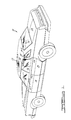
- a four-door sedan type automotive vehicle 10 is shown as employing the keyless entry system of the present invention, and includes a five pushbutton keyboard K-1 on the upper portion of the left front door 18. commonly referred to as the " driver's " door.
- the presented embodiment also provides for an additional keyboard K-2 similarly mounted on the front right door 18', commonly referred to as the " front passenger's " door.
- the vehicle 10 also includes an electrically releasable rear decklid 22 covering a rear storage compartment.
- the rear decklid 22 contains an electrically actuated unlocking mechanism, of conventional design, that is released by a switch located within the vehicle and, in this embodiment, is additionally controlled for release by the keyless entry system.
- the vehicle 10 is further shown as including an electrically retractable roof window 12, commonly know as a " sunroof ".
- the vehicle 10 includes electrically powered side windows 14 and 1,4', mounted in respective front doors 18 and 18', and electrically powered side windows 16 and 16' mounted in respective rear doors 20 and 20'.
- Each of the above mentioned electrically powered elements including the door locks, the rear deck lid 22, the roof window 12, and the electrically powered windows, are conventionally controlled by appropriate switches within the passenger compartment of the vehicle.
- these elements can also be controlled from outside the vehicle.
- the opening of the deck lid 22, from the outside of the vehicle without a key is a novel anti-theft feature since it eliminates the possibility of key cylinder " punch-out " by those attempting forced entry into the rear storage compartment.
- the control of the windows from outside the vehicle is especially desirable when one wishes to cool down the interior of the vehicle after it has been sitting for a period of time absorbing sunlight radiation. By retracting the roof window and/or lowering the side windows from the outside of the vehicle, it is possible to allow the hot air trapped inside the passenger compartment to escape before entering.
- a driver door switch assembly K-1 and a similar passenger door switch assembly K-2 are each shown as comprising five pushbutton switches respectively designated with digital values of " 1 ", " 2 ", “ 3 ", “ 4 " and “ 5 ". Whenever any one of the pushbuttons on either assembly is depressed, that event is detected by an activate/reset timer-32 through an eleven diode array (D-1,... D-11) shown in Figure 3.
- the activate/reset timer 32 is used to generate an activate signal to an illuminated entry module 30 in response to any depressed pushbutton.
- the illuminated entry module 30 is a conventional relay circuit which, when activated, energizes selected lamps, such as those in the passenger compartment of the vehicle and, in this case, lamps which illuminate the keyboards. Illumination of the keyboard is a convenience feature which allows the user to operate the keyboard in darkness and which informs the user that the system is activated to receive coded inputs.
- the activate/reset timer 32 provides an output signal to the illuminated entry module 30 through a timer circuit T-1 for a period of time which is generally selected to be in the range of approximately five to twenty seconds. Selection of values for the resistor 101 and capacitor 102 determine the period of time. In this case, values of 1 M ohm and 10 ⁇ f were respectively selected to give a time period of approximately 16.5 seconds.
- the timer circuit T-1 is a monostable multi-vibrator. such as that commercially designated as 14528. As each subsequent pushbutton is depressed, the activate/reset timer 32 continues to output an activating signal to the illuminated entry module 30, since each subsequently depressed pushbutton restarts the time period.
- the negative going signal from the timer T-1 is output through capacitor 103 as a SYSTEM RESET signal.
- the SYSTEM RESET signal is used to reset the various components of the system and to specifically inhibit comparators 44 and 46, which are more fully described below.
- the outputs of the switch assemblies K-1 and K-2 are directly fed to a priority switch selector 34. for gating.
- the priority switch selector 34 is shown in detail in Figure 3 and referred to in the following description.
- primary priority of control operation is assigned to the driver switch assembly K-1 and secondary priority is assigned to the passenger switch assembly K-2.
- the signal inputs from the switch assembly K-1 are commonly connected through diodes D-7 through D-11 to set a flip-flop 201 and produce a Q output signal whenever one of the pushbuttons of the assembly K-1 is depressed.
- the setting of the flip-flop 201 enables the
- the channel selectors 202 and 203 are commercially designated as 14519 and are connected to gate through the five digital signals from the switch assembly K-1 (A channel). whenever any one of the pushbuttons on the assembly K-1 is depressed. Otherwise, the flip-flop 201 is in its reset condition and the Q output signal enables the " B " channel selector inputs of the two channel data selectors 202 and 203. In this case, the digital signals from the switch assembly K-2 (B Channel) are gated through the channel selectors 202 and 203, when the flip-flop 201 is reset. The signals from the keyboard of the selected channel are correspondingly gated through on output lines 41, 42, 43, 44 and 45 as respective digital value signals.
- the priority switch selector 34 outputs channel designating signals on lines 33 and 35. which respectively correspond to the selected A and B channels.
- the output signals on lines 33 and 35 respectively enable corresponding AND gate logic circuitry 62 or 64 which controls unlocking of the door corresponding to the keyboard switch assembly selected to have control.
- the inputs to the switch assembly K-2 are gated through the priority switch selector 34 until such time as a pushbutton is depressed on the switch assembly K-2 is disabled in favour of subsequent signals coming from the switch assembly K-1 within the predetermined time period.
- the user may enter the proper codes into the driver switch assembly K-1 without interference from someone else indiscriminately depressing various pushbuttons on the switch assembly K-2.
- the passenger switch assembly K-2 is omitted, leaving only one switch assembly K-1 mounted on the driver's door.
- the priority switch selector 34 is also omitted.
- the gated digital value signals on lines 41 4 2. 43, 44 and 45 are connected to a switch debounce circuit 36.
- a commercially designated module 14490 is used.
- the switch debounce circuit is used for the elimination of extraneous voltage level changes that occasionally result due to the interfacing of the electronics with the mechanical contacts of the keyboarcs.
- the circuit takes an input signal form a bouncing contact and generates a clean digital signal. This eliminates the possibility of the circuit seeing switch chatter as multiple pulses.
- the output of the switch debounce circuit 36 is connected to a digital-to-BCD converter 38. where the digital value signals are converted to binary code and output on three lines.
- the digital-to-BCD converter selected for this embodiment is commercially designated as 14532 and has a G, output for every signal input.
- the G, output is used to trigger clocking signals in a conventional clocking generator circuit 39.
- the output of the clocking generator circuit 39 contains both cl and cl signals.
- the BCD output from the converter 38 is connected to a ROM comparator 44, a RAM comparator 53. and a user programmable RAM 52.
- a ROM address counter 48 is initially set to a zero count (first address) and its output is connected to address a ROM permanent memory 42.
- the permanent memory 42 is detailed in Figure 10 as being wired (preprogrammed) for the sequentially entered code of 2-4-1-3-5. It should be understood that the diodes shown in the permanent ROM memory 42 correspond to one wiring arrangement of 3.125 possible arrangements and correspond to one digital code of 3,125 possible digital codes. Of course. a greater number of codes are possible if the number of data lines and corresponding number of pushbutton keys are expanded.
- the ROM address counter 48 When the ROM address counter 48 is at a zero count, the corresponding first address D, to the ROM 42 causes a 0-1-0 (2) to appear at the corresponding B o -B-B 2 output line and input to the ROM comparator 44.
- Each BCD output from the converter 38, corresponding to digital value signal, is compared in the ROM comparator 44 with the addressed contents of the memory 42.
- the second address causes a 0-0-1 (4) to appear at the corresponding B 0 -B 1 -B 2 input to the comparator 44.
- the ROM address counter 48 As each BCD signal from the converter 38 is compared in the comparator 44 and found to be equal to the addressed contents of the memory 42, the ROM address counter 48 is advanced. After the ROM address counter 48 has advanced five times (sixth address), a FIRST ENABLE signal is output from the counter 48 and is gated through an OR gate logic 60 to a latch 61 and provinces a FUNCTION ENABLING signal to AND gate logic circuits 62, 64, 66, 68, 70 and 72.
- the RAM comparator 53 is also commercially designated as 14585 and operates in parallel with the ROM comparator 44 to simultaneously compare each digital value signal as converted by the BCD converter 38 with the read-out contents of the user programmable RAM 52.
- a type 14552 RAM was selected for the user programmable RAM 52. Assuming it has been programmed, the RAM 52 is sequentially addressed for read-out by the BCD output of the RAM address counter 50. The data read-out at terminals D out o - D out 1 - D out 2 , from the user programmable RAM 52 is input to the RAM comparator 53 at corresponding input terminals B O -B I -B 2 . The data read-out from the user programmable RAM 52 is then compared with the converted digital value signals input to terminals A O -A l -A 2 . A fourth data input terminal A3 is compared with a corresponding data input terminal B 3 .
- the data input terminal A3 is grounded and the data input terminal B 3 is normally held to zero by a RAM comparator disable logic 58.
- the RAM comparator disable logic 58 functions to supply a " 1 " to the data input terminal B 3 of the RAM comparator 53 whenever the user operates the system to disable the optional user programmable code feature of the system in favour of exclusive permanent code operation.
- the disable logic 58 is explained in greater detail below.
- a SECOND ENABLE signal is responsively output from an NAND gate 59 to the OR gate 60, mentioned above.
- the input to the NAND gate 59 corresponds to the A o and A 2 address output from the RAM address counter 50. Since these addresses are in BCD, a simultaneous appearance of " 1 ", at both the A o and A 2 address outputs, corresponds to the sixth address of the RAM address counter 50. This signifies that the five preceeding digital value signals input to the RAM comparator 53 have been found to positively match the corresponding five data values read-out from the user programmable RAM 52.
- the occurrence of either the FIRST ENABLE signal or the SECOND ENABLE signal to the OR gate 6 0 causes a setting of the latch 61. which produces the FUNCTION ENABLING signal to enable occurrence of the subsequent functions in response to appropriate commands.
- one of the subsequent functions is enabled exclusively by the FIRST ENABLE Signal. That function allows the user to programme the user programmable RAM 52 with a new user selected code having five digital values. This is achieved by entering the permanent code into a selected keyboard to cause the ROM address counter 48 to produce the FIRST ENABLE signal.
- the FIRST ENABLE signal is connected to the input of a write enable logic circuit 56, which is shown in detail in Figure 5.
- the FIRST ENABLE signal from the ROM address counter 48 is used to set a latch 84, which enables and AND gate 82.
- the user In order to produce a WRITE ENABLE-(not) signal as an output of the write enable logic circuit 56, the user must depress the 1 button on a selected keyboard following the insertion of the permanent code. If another pushbutton is depressed immediately following the insertion of the permanent code, a correspondingly designated function occurs, but the WRITE-enable-(not) signal is not generated until the 1 button is depressed.
- a latch 86 will be set and thereby generate a WRITE ENABLE -(not) signal, to the WRITE ENABLE terminal We on the user programmable RAM 52. through an inverter 87.
- the output signal from the latch 86 is also fed to AND gate 80.
- Other inputs to AND gate 80 are connected to receive addresses A o and A 2 from the RAM address counter 50 to indicate a fifth advance (sixth address) of the RAM address counter 50.
- the WRITE ENABLE -(not) signal places the user programmable RAM 52 in the WRITE mode so that the next five sequentially entered digits will be correspondingly stored in the user programmable RAM 52.
- the WRITE ENABLE -(not) signal from the write enable logic 56 also is connected as the second of two inputs to disable an AND gate 54 and thereby prevent the resetting of the RAM address counter 50 during the WRITE mode of the user programmable RAM 52, and to enable the gate 54 when the user programmable RAM 52 is in the READ mode.
- the AND gate 80 outputs a signal a long line 57 to immediately reset the activate/reset timer 32.
- a SYSTEM RESET signal is then generated by the activate/reset timer 32, which resets and deactivates the entire system. This immediate resetting of the system, following the writing-in of the new user selected code. allows the user to immediately reenter the new code and check to see that it is correct and operational.
- the RAM comparator disable logic 58 incorporates a NOR gate 92, which receives the three outputs of the RAM address counter 50 and generates a " 1 " when the RAM address counter50 is at its zero count level (first address).
- the output of the NOR gate 92 is connected to one input of a NAND gate 94.
- a second input to the NAND gate 94 is connected to receive the output signal from latch 86, while a third input is received from the (5 output of timer T-1.
- the output of the NAND gate 94 is connected to the 9 terminal of a latch 96 to set the latch 96 when the latch 86 is set and no subsequent digits are entered into the system.
- the output of the latch 96 is connected to the B 3 terminal of the RAM comparator 53.
- the latch 96 will be set to inhibit a true comparison in the RAM comparator 53 when the user fails to enter a complete fivedigit new used selected code following the entry of the permanent code and the digit " 1 ".
- the latch 96 is reset to produce a " 0 " output to B 3 of the RAM comparator 53 when a new user selected code is written into the user programmable RAM 52 by the inverted output of AND gate 80.
- the AND gate logic circuit 66 comprises a NAND gate 101 which receives the FUNCTION ENABLING signal from latch 61 and the 2 digital value signal from the switch debounce circuit 36.
- the output of the NAND gate 101 is connected to a latch 102, which has its output connected to activate a driving transistor Q6.
- the collector of the transistor Q6 is connected to a conventional electrically activated relay (not shown) for unlocking all the doors of the vehicle.
- An AND gate logic circuit 68 is shown in Figures 2 and 7, which gates through a 3 digital value signal from the switch debounce circuit 36 when enabled by the FUNCTION ENABLING signal from latch 61 to effect unlocking of the deck lid by activating an electrically energizable deck lid lock relay (not shown).
- the AND gate logic circuit 68 comprises a NAND gate 201, a latch 202, and a transistor Q5.
- the AND gate logic circuit 68 is substantially identical to the AND gate logic circuit 66 shown is Figures 2 and 6.
- An AND gate logic circuit 70 is shown in Figures 2 and 8, wherein a digital value signal 4 is gated by the FUNCTION ENABLING signal from latch 61 to energize a motor of a retractable sunroof.
- the AND gate logic circuit 70 comprises a feedback circuit, wherein the sunroof motor is monitored so that when the sunroof motor enters a stalled condition, that condition will be sensed and the sunroof motor will then be de-energized.
- the AND gate logic circuit 70 comprises a NAND gate 301 which, upon receiving a FUNCTION ENABLING signal from latch 61 and a 4 digital value signal, sets a latch 302 that in turn energizes transistor Q7.
- the collector of the transistor Q7 is connected to the sunroof motor to cause retraction of the sunroof.
- a comparator 304 is connected to monitor the voltage across the sunroof motor. When the sunroof motor becomes stalled (fully retracted), the voltage level will change and that change will be compared against a preset level at potentiometer 305, which is connected to a second input of the comparator 304. A sensed difference between the voltage inputs to the comparator 304 is gated through NAND gate 303 to reset the latch 302.
- An AND gate logic circuit 72 is shown in Figures 2 and 9 and functions to gate a first 5 digital value signal through an enabled NAND gate 401 to set a latch 402 to thereby energize a drive transistor Q8 and effect lowering of the front side windows of the vehicle.
- a feedback circuit similar to that shown in Figure 8, is included to reset the latch 402 and terminate drive of the front window motors when they are fully lowered and the motors reach stalled condition.
- the feedback circuit comprises potentiometer 405, a comparator 404, and a NAND gate 403, which are wired in substantially the same manner as shown in Figure 8.
- the AND gate logic circuit 72 functions to store a second 5 digital value signal which is entered into the keyboard prior to the generation of the SYSTEM RESET signal by the activate/reset timer 32. This is necessitated by the fact that the activate/reset timer 32 may have a time-out period which is less than the time it takes to lower the front side windows. Therefore, the firs inserted 5 digital value signal causes the front side windows to be lowered and the second entered 5 digital value signal is stored to effect lowering of the rear side windows following completion of the lowering of the front side windows. This is accomplished by a divider circuit 410, which is a dual type D flip-flop 140 1 3. The divider 410 is connected to receive the output of the NAND gate 401.
- the first 5 digital value signal gated through the NAND gate 401 is clocked into the divider 410 and the second 5 digital value signal gated through the NAND gate 401 causes the divider 410 to output a " 0 " signal to a NOR gate 406.
- a second input terminal of the NOR gate 406 is connected to receive the output of NAND gate 403 in the feedback line from the front window motors. Therefore, when both the input terminals to NOR gate 406 are " 0 " the NOR gate 406 produces a " 1 " which is inverted by an inverter 407 to set a latch 412.
- the set latch 412 energizes a drive transistor Q9, which is connected to a relay for energizing the motors of the side rear windows and cause the lowering thereof.
- a feedback circuit comprising a potentiometer 415, a comparator 414, and a NAND gate 413 are connected in a manner, as discussed in the abovementioned feedback circuits, to reset the latch 412 when the rear window motors are fully lowered.
- the system described above with reference to the drawings allows the user the option of utilizing a permanent code or a user- selected code to gain entry to the vehicle in which the system is installed.
- the user may also effect a number of functions from outside the vehicle which heretofore could only be effected from inside the passenger compartment of the vehicle.
- the system also has the advantage of deactivating and resetting itself a predetermined time after the last digit has been entered, and of becoming activated upon the entering of any digit.
- the system includes dual keyboards for mounting on opposite doors of the vehicle, one keyboard having operational priority over the other.
Description
- The present invention is directed to a keyless entry system, and, more particularly, to a system which permits a driver and passengers to enter a locked vehicle without the use of keys, while at the same time maintaining a high degree of security for the vehicle.
- Several electrical systems have been devised for automotive vehicles, which allow persons know ledgeable of a predetermined combination to unlock a vehicle by entering that combination into an electronic switch keyboard mounted on the outside of the vehicle.
- U.S. Patent No. 3,544,804, discloses a system utilizing keyboards respectively mounted on the outside of the driver's door and on the dash. The keyboards each have numbered keys or pushbuttons which, when depressed, actuate corresponding switches. The switches, in turn, operate relay components of a register. When the proper combination is formed by sequential actuation of the keys, a lock release solenoid in the door, in the case of the door keyboard, or the starter circuit of the vehicle engine, in the case of the dash keyboard, may be respectively energized to open the door or start the vehicle. The electrical connection between particular pushbuttons of the keyboard and the sequentially actuated relays may be physically changed through the use of a plug and jack patch panel, located in the trunk of the vehicle, to effect a combination change.
- U.S. Patent No. 3.691.396 discloses an electronic combination door and ignition lock which requires insertion of a predetermined code containing repeated symbols from a keyboard unit mounted on the exterior of the vehicle in order to obtain entry to the vehicle. As above, a second keyboard is contained within the vehicle to allow energization of the ignition system of the vehicle upon the reinsertion of the same predetermined code. The system includes a hard wired logic network that gates through a predetermined sequence of keyboard entered digits and resets the system when any digit is entered, which is out of the predetermined sequence.
- Both of the systems discussed above, are rigidly set up so as to cause deactivation (or resetting) of the respective systems when any error is made while entering a single predetermined combination of digits. Those systems are further limited in the number of functions that may be performed while outside the vehicle and do not provide for a reprogrammable system to supplement a permanently programmed system.
- U.S. Patent No 3766400 discloses a keyless locking system which includes a hard-wired logic network which is responsive to either a primary or a secondary digit code, as required by the operator. U.S. Patent No 3754213 discloses a keyless locking system suitable for a building in which an input code entered by the user wishing to open the door is compared with a code for the door set in a central memory controlled separately from the door, and an unlocking signal is generated if the comparison is correct.
- According to the present invention, there is provided a keyless locking system for use in an automotive vehicle comprising entering means for entenng a multi digit code into the system in the form of electrical signals : means for permanently storing a first code representing a sequence of digits : means for storing a second code representing a sequence of digits and means for unlocking one or more locks on the vehicle when the entered code corresponds to either of the stored codes, characterised by comparator means for sequentially comparing the digits of a multi digit code entered into the system with the successive digits of the first and second codes and for generating first or second enabling signals when the code entered into the system corresponds with either the first or second code, the unlocking means being operable in response to the first or second enabling signals, and further characterised in that the means for storing the second code is programmable by the user of the system.
- The present invention is seen as an improvement over the prior art in that several functions are incorporated in a single keyless entry system for an automotive vehicle. Major improved features include a permanent preprogrammed code storage memory and a user-programmable code storage memory, wherein either code may be inserted into the system to gain entry into the vehicle and enable the other function. The other functions include the ability to unlock one or several doors of the vehicle, retract a roof-window, unlock a deck lid, lower selected side windows, reprogramme a new used selected code into the programmable memory or disable the system response to the user selected code. These functions have been found to be highly desirable since they can be controlled to occur prior to entering the vehicle.
- Five digit designated pushbutton keyboards on opposite vehicle doors are shown in the preferred embodiment, as the means by which all predetermined codes are manually entered into the system. A primary keyboard mounted on the left front (driver's) door is designated by the system to have continual override priority over the keyboard mounted on the right front (passenger's) door. However, each keyboard has independent operational capability to allow a user to enter correct digit codes and have the system perform the aforementioned functions.
- In operation, a depression of any pushbutton on either keyboard will cause illumination of the keyboard, activation of the system, and may also cause illumination of the vehicle interior for a predetermined period of time. In this manner, the system is visible for night operation and activated to receive a multi-digit code which corresponds to either the permanent preprogrammed code or a programmed user selected code. The user then depresses a sequence of digitally designated pushbuttons and each depression commences a new time period for illumination and activation, In order to eliminate excessive battery drain, the system will deactivate and illumination will terminate if the user hesitates longer tha the predermi- ned time period. When proper entering of either the permanent or user selected multi-digit code is made, the door, upon which the particular keyboard is mounted, will immediately unlock and allow entry to the passenger compartment of the vehicle. Subsequently, while the system remains activated during the aforementioned time period, predetermined digital pushbuttons may be depressed to unlock all the other vehicle doors, unlock the deck lid, retract a roof-window, lower the side window, programme a new user selected code into the programmable memory, or disable the system response to the last programmed user selected code.
- A preferred embodiment of the invention will now be described, by way of example only, with reference to the drawings, in which :
- Figure 1 illustrates an automotive vehicle incorporating a keyless entry system in accordance with the invention and specifically shows the preferred location of the digital input keyboards ;
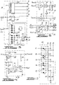
- Figures 2 A and 2 B together show an overall block diagram illustrating the various logic functions of the system ;
- Figure 3 is a detailed schematic diagram of the priority switch selector shown in Figure 2 ;
- Figure 4 is a detailed schematic diagram of the activate/reset timer shown in Figure 2 ;
- Figure 5 is a detailed schematic diagram of both the RAM comparator disable logic and write enable logic shown in Figure 2 ;
- Figure 6 is a detailed schematic diagram of the AND
gate logic circuit 66 shown in Figure 2 ; - Figure 7 is a detailed schematic diagram of the AND
gate logic circuit 68 shown in Figure 2 ; - Figure 8 is a detailed schematic diagram of the AND
gate logic circuit 70 shown in Figure 2 ; - Figure 9 is a detailed schematic diagram of the AND
gate logic circuit 72 shown in Figure 2 ; and - Figure 10 is a detailed schematic diagram of the ROM
permanent memory 42 shown in Figure 2. - Referring now to Figure 1, a four-door sedan type automotive vehicle 10 is shown as employing the keyless entry system of the present invention, and includes a five pushbutton keyboard K-1 on the upper portion of the
left front door 18. commonly referred to as the " driver's " door. The presented embodiment also provides for an additional keyboard K-2 similarly mounted on the front right door 18', commonly referred to as the " front passenger's " door. The vehicle 10 also includes an electrically releasablerear decklid 22 covering a rear storage compartment. Therear decklid 22 contains an electrically actuated unlocking mechanism, of conventional design, that is released by a switch located within the vehicle and, in this embodiment, is additionally controlled for release by the keyless entry system. The vehicle 10 is further shown as including an electricallyretractable roof window 12, commonly know as a " sunroof ". In addition, the vehicle 10 includes electrically poweredside windows front doors 18 and 18', and electrically poweredside windows 16 and 16' mounted in respectiverear doors 20 and 20'. - Each of the above mentioned electrically powered elements, including the door locks, the
rear deck lid 22, theroof window 12, and the electrically powered windows, are conventionally controlled by appropriate switches within the passenger compartment of the vehicle. In addition, these elements can also be controlled from outside the vehicle. The opening of thedeck lid 22, from the outside of the vehicle without a key, is a novel anti-theft feature since it eliminates the possibility of key cylinder " punch-out " by those attempting forced entry into the rear storage compartment. On the other hand, the control of the windows from outside the vehicle is especially desirable when one wishes to cool down the interior of the vehicle after it has been sitting for a period of time absorbing sunlight radiation. By retracting the roof window and/or lowering the side windows from the outside of the vehicle, it is possible to allow the hot air trapped inside the passenger compartment to escape before entering. - Referring to Figure 2, the principle of operation is shown. A driver door switch assembly K-1 and a similar passenger door switch assembly K-2 are each shown as comprising five pushbutton switches respectively designated with digital values of " 1 ", " 2 ", " 3 ", " 4 " and " 5 ". Whenever any one of the pushbuttons on either assembly is depressed, that event is detected by an activate/reset timer-32 through an eleven diode array (D-1,... D-11) shown in Figure 3.
- The activate/
reset timer 32, shown in detail in Figure 4, is used to generate an activate signal to anilluminated entry module 30 in response to any depressed pushbutton. Theilluminated entry module 30 is a conventional relay circuit which, when activated, energizes selected lamps, such as those in the passenger compartment of the vehicle and, in this case, lamps which illuminate the keyboards. Illumination of the keyboard is a convenience feature which allows the user to operate the keyboard in darkness and which informs the user that the system is activated to receive coded inputs. - The activate/
reset timer 32 provides an output signal to theilluminated entry module 30 through a timer circuit T-1 for a period of time which is generally selected to be in the range of approximately five to twenty seconds. Selection of values for the resistor 101 andcapacitor 102 determine the period of time. In this case, values of 1 M ohm and 10 µf were respectively selected to give a time period of approximately 16.5 seconds. The timer circuit T-1 is a monostable multi-vibrator. such as that commercially designated as 14528. As each subsequent pushbutton is depressed, the activate/reset timer 32 continues to output an activating signal to the illuminatedentry module 30, since each subsequently depressed pushbutton restarts the time period. When the aforementioned time period elapses following the last depression of a pushbutton, the negative going signal from the timer T-1 is output throughcapacitor 103 as a SYSTEM RESET signal. The SYSTEM RESET signal is used to reset the various components of the system and to specifically inhibitcomparators - The outputs of the switch assemblies K-1 and K-2 are directly fed to a
priority switch selector 34. for gating. Thepriority switch selector 34 is shown in detail in Figure 3 and referred to in the following description. - In this embodiment of the invention, primary priority of control operation is assigned to the driver switch assembly K-1 and secondary priority is assigned to the passenger switch assembly K-2. To achieve selection, the signal inputs from the switch assembly K-1 are commonly connected through diodes D-7 through D-11 to set a flip-
flop 201 and produce a Q output signal whenever one of the pushbuttons of the assembly K-1 is depressed. The setting of the flip-flop 201 enables the - A " channel selector inputs of two
channel data selectors channel selectors flop 201 is in its reset condition and the Q output signal enables the " B " channel selector inputs of the twochannel data selectors channel selectors flop 201 is reset. The signals from the keyboard of the selected channel are correspondingly gated through onoutput lines - In addition to selecting and gating a channel, the
priority switch selector 34 outputs channel designating signals onlines lines gate logic circuitry 62 or 64 which controls unlocking of the door corresponding to the keyboard switch assembly selected to have control. - In operation, the inputs to the switch assembly K-2 are gated through the
priority switch selector 34 until such time as a pushbutton is depressed on the switch assembly K-2 is disabled in favour of subsequent signals coming from the switch assembly K-1 within the predetermined time period. In this configuration, the user may enter the proper codes into the driver switch assembly K-1 without interference from someone else indiscriminately depressing various pushbuttons on the switch assembly K-2. - In an alternative embodiment (not shown), the passenger switch assembly K-2 is omitted, leaving only one switch assembly K-1 mounted on the driver's door. In such an alternative embOdI- ment. the
priority switch selector 34 is also omitted. - The gated digital value signals on
lines 41 42. 43, 44 and 45 are connected to aswitch debounce circuit 36. In this embodiment. a commercially designatedmodule 14490 is used. The switch debounce circuit is used for the elimination of extraneous voltage level changes that occasionally result due to the interfacing of the electronics with the mechanical contacts of the keyboarcs. The circuit takes an input signal form a bouncing contact and generates a clean digital signal. This eliminates the possibility of the circuit seeing switch chatter as multiple pulses. The output of theswitch debounce circuit 36 is connected to a digital-to-BCD converter 38. where the digital value signals are converted to binary code and output on three lines. - The digital-to-BCD converter selected for this embodiment is commercially designated as 14532 and has a G, output for every signal input. The G, output is used to trigger clocking signals in a conventional clocking generator circuit 39. The output of the clocking generator circuit 39 contains both cl and
cl signals. The BCD output from the converter 38 is connected to aROM comparator 44, a RAM comparator 53. and a userprogrammable RAM 52. - A
ROM address counter 48 is initially set to a zero count (first address) and its output is connected to address a ROMpermanent memory 42. Thepermanent memory 42 is detailed in Figure 10 as being wired (preprogrammed) for the sequentially entered code of 2-4-1-3-5. It should be understood that the diodes shown in thepermanent ROM memory 42 correspond to one wiring arrangement of 3.125 possible arrangements and correspond to one digital code of 3,125 possible digital codes. Of course. a greater number of codes are possible if the number of data lines and corresponding number of pushbutton keys are expanded. - When the
ROM address counter 48 is at a zero count, the corresponding first address D, to theROM 42 causes a 0-1-0 (2) to appear at the corresponding Bo-B-B2 output line and input to theROM comparator 44. Each BCD output from the converter 38, corresponding to digital value signal, is compared in theROM comparator 44 with the addressed contents of thememory 42. In this case, theROM comparator 44 is commercially designated as 14585. Therefore. when theROM address counter 48 is at a zero count and when a digital value signal corresponding to the 2 pushbutton is entered. theROM comparator 44 will output a " 1 " on its A = B output terminal. This output signal is then input to anNAND gate 46 which, through anOR gate 47. inhibits the resetting to theROM address counter 48. The inhibiting of the reset allows thecounter 48 to be advanced by one count upon the input of the next cl signal. Therefore. the second address causes a 0-0-1 (4) to appear at the corresponding B0-B1-B2 input to thecomparator 44. - As each BCD signal from the converter 38 is compared in the
comparator 44 and found to be equal to the addressed contents of thememory 42, theROM address counter 48 is advanced. After theROM address counter 48 has advanced five times (sixth address), a FIRST ENABLE signal is output from thecounter 48 and is gated through anOR gate logic 60 to alatch 61 and provinces a FUNCTION ENABLING signal to ANDgate logic circuits - The RAM comparator 53 is also commercially designated as 14585 and operates in parallel with the
ROM comparator 44 to simultaneously compare each digital value signal as converted by the BCD converter 38 with the read-out contents of the userprogrammable RAM 52. ARAM address counter 50 operates in a manner similar to theROM address counter 48 to sequentially advance to its next address whenever an A = B output signal is generated by the RAM comparator 53. - A
type 14552 RAM was selected for the userprogrammable RAM 52. Assuming it has been programmed, theRAM 52 is sequentially addressed for read-out by the BCD output of theRAM address counter 50. The data read-out at terminals Douto-Dout1-Dout2, from the userprogrammable RAM 52 is input to the RAM comparator 53 at corresponding input terminals BO-BI-B2. The data read-out from the userprogrammable RAM 52 is then compared with the converted digital value signals input to terminals AO-Al-A2. A fourth data input terminal A3 is compared with a corresponding data input terminal B3. In this configuration, the data input terminal A3 is grounded and the data input terminal B3 is normally held to zero by a RAM comparator disablelogic 58. Briefly, the RAM comparator disablelogic 58 functions to supply a " 1 " to the data input terminal B3 of the RAM comparator 53 whenever the user operates the system to disable the optional user programmable code feature of the system in favour of exclusive permanent code operation. The disablelogic 58 is explained in greater detail below. - Whenever the data inputs to the RAM comparator 53, from the user
programmable RAM 52, are found to respectively correspond to the data inputs from the converted digital value signals, the RAM comparator 53 outputs and A = B signal to aNAND gate 55. The occurrence of the A = B signal causes a " 0 " output therefrom which is connected to the input of an AND gate 54. A second input to AND gate 54, is the WRITE ENABLE -(not) signal from logic56. Therefore, when theRAM 52 is in the READ mode, a " 1 " signal from the NORgate 55 is gated through the enabled AND gate 54 to effect resetting of theRAM address counter 50, if no A = B signal is output from the RAM comparator 53 during a 6-1 pulse. After theRAM address counter 50 has advanced five times, to its sixth address, a SECOND ENABLE signal is responsively output from anNAND gate 59 to theOR gate 60, mentioned above. The input to theNAND gate 59 corresponds to the Ao and A2 address output from theRAM address counter 50. Since these addresses are in BCD, a simultaneous appearance of " 1 ", at both the Ao and A2 address outputs, corresponds to the sixth address of theRAM address counter 50. This signifies that the five preceeding digital value signals input to the RAM comparator 53 have been found to positively match the corresponding five data values read-out from the userprogrammable RAM 52. The occurrence of either the FIRST ENABLE signal or the SECOND ENABLE signal to theOR gate 60 causes a setting of thelatch 61. which produces the FUNCTION ENABLING signal to enable occurrence of the subsequent functions in response to appropriate commands. - However, one of the subsequent functions is enabled exclusively by the FIRST ENABLE Signal. That function allows the user to programme the user
programmable RAM 52 with a new user selected code having five digital values. This is achieved by entering the permanent code into a selected keyboard to cause theROM address counter 48 to produce the FIRST ENABLE signal. The FIRST ENABLE signal is connected to the input of a write enablelogic circuit 56, which is shown in detail in Figure 5. The FIRST ENABLE signal from theROM address counter 48 is used to set a latch 84, which enables and AND gate 82. In order to produce a WRITE ENABLE-(not) signal as an output of the write enablelogic circuit 56, the user must depress the 1 button on a selected keyboard following the insertion of the permanent code. If another pushbutton is depressed immediately following the insertion of the permanent code, a correspondingly designated function occurs, but the WRITE-enable-(not) signal is not generated until the 1 button is depressed. - Providing the 1 digital value signal is generated and applied to the enabled AND gate 82, a
latch 86 will be set and thereby generate a WRITE ENABLE -(not) signal, to the WRITE ENABLE terminal We on the userprogrammable RAM 52. through aninverter 87. The output signal from thelatch 86 is also fed to ANDgate 80. Other inputs to ANDgate 80 are connected to receive addresses Ao and A2 from theRAM address counter 50 to indicate a fifth advance (sixth address) of theRAM address counter 50. Therefore, when a new user selected code is being programmed into the userprogrammable RAM 52, following the insertion of the permanent code and the subsequently entered 1, the WRITE ENABLE -(not) signal places the userprogrammable RAM 52 in the WRITE mode so that the next five sequentially entered digits will be correspondingly stored in the userprogrammable RAM 52. - The WRITE ENABLE -(not) signal from the write enable
logic 56 also is connected as the second of two inputs to disable an AND gate 54 and thereby prevent the resetting of theRAM address counter 50 during the WRITE mode of the userprogrammable RAM 52, and to enable the gate 54 when the userprogrammable RAM 52 is in the READ mode. - Following the writing-in of the fifth digit of a new user selected code. the AND
gate 80 outputs a signal along line 57 to immediately reset the activate/resettimer 32. A SYSTEM RESET signal is then generated by the activate/resettimer 32, which resets and deactivates the entire system. This immediate resetting of the system, following the writing-in of the new user selected code. allows the user to immediately reenter the new code and check to see that it is correct and operational. - If, on the other hand, the user wishes to inhibit the user selected code portion of the system, he merely enters the permanent code followed by the 1 and waits for the activate/reset
timer 32 to reset the system. That sequence prevents the RAM comparator 53 from producing A = B signals until a new user selected code is subsequently programmed into the system, since the B3 input line to the comparator 53 is latched to a " 1 " level by the RAM comparator disablelogic circuit 58. - The RAM comparator disable
logic 58, shown in detail in Figure 5, incorporates a NOR gate 92, which receives the three outputs of theRAM address counter 50 and generates a " 1 " when the RAM address counter50 is at its zero count level (first address). The output of the NOR gate 92 is connected to one input of aNAND gate 94. A second input to theNAND gate 94 is connected to receive the output signal fromlatch 86, while a third input is received from the (5 output of timer T-1. The output of theNAND gate 94 is connected to the 9 terminal of alatch 96 to set thelatch 96 when thelatch 86 is set and no subsequent digits are entered into the system. The output of thelatch 96 is connected to the B3 terminal of the RAM comparator 53. In this configuration, thelatch 96 will be set to inhibit a true comparison in the RAM comparator 53 when the user fails to enter a complete fivedigit new used selected code following the entry of the permanent code and the digit " 1 ". Thelatch 96 is reset to produce a " 0 " output to B3 of the RAM comparator 53 when a new user selected code is written into the userprogrammable RAM 52 by the inverted output of ANDgate 80. - Other functions are now described which can be commanded by depressing predetermined pushbuttons following the generation of either the FIRST ENABLING signal or the SECOND ENABLING signal.
- An AND
gate logic circuit 66 is shown in Figures 2 and 6. The ANDgate logic circuit 66 comprises a NAND gate 101 which receives the FUNCTION ENABLING signal fromlatch 61 and the 2 digital value signal from theswitch debounce circuit 36. The output of the NAND gate 101 is connected to alatch 102, which has its output connected to activate a driving transistor Q6. The collector of the transistor Q6 is connected to a conventional electrically activated relay (not shown) for unlocking all the doors of the vehicle. An ANDgate logic circuit 68 is shown in Figures 2 and 7, which gates through a 3 digital value signal from theswitch debounce circuit 36 when enabled by the FUNCTION ENABLING signal fromlatch 61 to effect unlocking of the deck lid by activating an electrically energizable deck lid lock relay (not shown). The ANDgate logic circuit 68 comprises aNAND gate 201, alatch 202, and a transistor Q5. The ANDgate logic circuit 68 is substantially identical to the ANDgate logic circuit 66 shown is Figures 2 and 6. - An AND
gate logic circuit 70 is shown in Figures 2 and 8, wherein adigital value signal 4 is gated by the FUNCTION ENABLING signal fromlatch 61 to energize a motor of a retractable sunroof. In addition to identical AND gate logic circuitry as that shown in Figures 6 and 7. the ANDgate logic circuit 70 comprises a feedback circuit, wherein the sunroof motor is monitored so that when the sunroof motor enters a stalled condition, that condition will be sensed and the sunroof motor will then be de-energized. The ANDgate logic circuit 70 comprises aNAND gate 301 which, upon receiving a FUNCTION ENABLING signal fromlatch 61 and a 4 digital value signal, sets a latch 302 that in turn energizes transistor Q7. The collector of the transistor Q7 is connected to the sunroof motor to cause retraction of the sunroof. In the feedback circuit. acomparator 304 is connected to monitor the voltage across the sunroof motor. When the sunroof motor becomes stalled (fully retracted), the voltage level will change and that change will be compared against a preset level atpotentiometer 305, which is connected to a second input of thecomparator 304. A sensed difference between the voltage inputs to thecomparator 304 is gated throughNAND gate 303 to reset the latch 302. - An AND
gate logic circuit 72 is shown in Figures 2 and 9 and functions to gate a first 5 digital value signal through an enabledNAND gate 401 to set alatch 402 to thereby energize a drive transistor Q8 and effect lowering of the front side windows of the vehicle. A feedback circuit, similar to that shown in Figure 8, is included to reset thelatch 402 and terminate drive of the front window motors when they are fully lowered and the motors reach stalled condition. The feedback circuit comprisespotentiometer 405, acomparator 404, and aNAND gate 403, which are wired in substantially the same manner as shown in Figure 8. In addition, the ANDgate logic circuit 72 functions to store a second 5 digital value signal which is entered into the keyboard prior to the generation of the SYSTEM RESET signal by the activate/resettimer 32. This is necessitated by the fact that the activate/resettimer 32 may have a time-out period which is less than the time it takes to lower the front side windows. Therefore, the firs inserted 5 digital value signal causes the front side windows to be lowered and the second entered 5 digital value signal is stored to effect lowering of the rear side windows following completion of the lowering of the front side windows. This is accomplished by adivider circuit 410, which is a dual type D flip-flop 14013. Thedivider 410 is connected to receive the output of theNAND gate 401. The first 5 digital value signal gated through theNAND gate 401 is clocked into thedivider 410 and the second 5 digital value signal gated through theNAND gate 401 causes thedivider 410 to output a " 0 " signal to a NORgate 406. A second input terminal of the NORgate 406 is connected to receive the output ofNAND gate 403 in the feedback line from the front window motors. Therefore, when both the input terminals to NORgate 406 are " 0 " the NORgate 406 produces a " 1 " which is inverted by aninverter 407 to set alatch 412. Theset latch 412 energizes a drive transistor Q9, which is connected to a relay for energizing the motors of the side rear windows and cause the lowering thereof. A feedback circuit comprising apotentiometer 415, acomparator 414, and aNAND gate 413 are connected in a manner, as discussed in the abovementioned feedback circuits, to reset thelatch 412 when the rear window motors are fully lowered. - It should be noted that in both the AND
gate logic circuits timer 32 may occur. However, due to the feedback circuits the ANDgate logic circuits - In summary, the system described above with reference to the drawings allows the user the option of utilizing a permanent code or a user- selected code to gain entry to the vehicle in which the system is installed. The user may also effect a number of functions from outside the vehicle which heretofore could only be effected from inside the passenger compartment of the vehicle. The system also has the advantage of deactivating and resetting itself a predetermined time after the last digit has been entered, and of becoming activated upon the entering of any digit. Moreover, the system includes dual keyboards for mounting on opposite doors of the vehicle, one keyboard having operational priority over the other.
Claims (17)
Applications Claiming Priority (2)
| Application Number | Priority Date | Filing Date | Title |
|---|---|---|---|
| US05/865,033 US4205325A (en) | 1977-12-27 | 1977-12-27 | Keyless entry system |
| US865033 | 1977-12-27 |
Publications (2)
| Publication Number | Publication Date |
|---|---|
| EP0002948A1 EP0002948A1 (en) | 1979-07-11 |
| EP0002948B1 true EP0002948B1 (en) | 1981-05-27 |
Family
ID=25344570
Family Applications (1)
| Application Number | Title | Priority Date | Filing Date |
|---|---|---|---|
| EP78300891A Expired EP0002948B1 (en) | 1977-12-27 | 1978-12-21 | Keyless locking and entry system |
Country Status (5)
| Country | Link |
|---|---|
| US (1) | US4205325A (en) |
| EP (1) | EP0002948B1 (en) |
| JP (1) | JPS54103199A (en) |
| CA (1) | CA1112736A (en) |
| DE (1) | DE2860741D1 (en) |
Families Citing this family (127)
| Publication number | Priority date | Publication date | Assignee | Title |
|---|---|---|---|---|
| DE2911160A1 (en) * | 1979-03-22 | 1980-10-02 | Daimler Benz Ag | DEVICE FOR PREVENTING UNAUTHORIZED STARTING OF VEHICLES |
| US4342210A (en) * | 1979-12-13 | 1982-08-03 | Denningham Clarence E | Vehicle entry locking arrangement |
| IT1130903B (en) * | 1980-01-29 | 1986-06-18 | Rbm Srl | BURGLAR ALARM ELECTRONIC AND COMBINATION EQUIPMENT FOR MOTOR VEHICLES IN GENERAL, VESSELS AND SIMILAR |
| JPS6019397B2 (en) * | 1981-04-30 | 1985-05-16 | 日産自動車株式会社 | Automatic door locking device for automobiles |
| JPS6017913B2 (en) * | 1981-04-30 | 1985-05-07 | 日産自動車株式会社 | electronic lock |
| US4335370A (en) * | 1981-05-21 | 1982-06-15 | Scalley Douglas M | Vehicle security device |
| US4492959A (en) * | 1981-06-24 | 1985-01-08 | Nissan Motor Company, Limited | Keyless entry system for an automotive vehicle |
| JPS5835694A (en) * | 1981-08-26 | 1983-03-02 | 日産自動車株式会社 | Anti-theft controller for automobile |
| JPS6047432B2 (en) * | 1981-10-02 | 1985-10-22 | 日産自動車株式会社 | electronic locking device |
| JPS6019395B2 (en) * | 1981-10-02 | 1985-05-16 | 日産自動車株式会社 | electronic locking device |
| JPS58120970A (en) * | 1982-01-14 | 1983-07-19 | 日産自動車株式会社 | Push button type electronic lock apparatus for vehicle |
| JPS58120969A (en) * | 1982-01-14 | 1983-07-19 | 日産自動車株式会社 | Push button type electronic lock apparatus for vehicle |
| JPS58139840A (en) * | 1982-02-15 | 1983-08-19 | Nissan Motor Co Ltd | Keyless vehicular load actuating device |
| JPS5924075A (en) * | 1982-07-30 | 1984-02-07 | 日産自動車株式会社 | Electric wave type key system |
| US4495540A (en) * | 1982-12-27 | 1985-01-22 | Presto Lock, Inc. | Electronic lock |
| JPS6064537A (en) * | 1983-09-19 | 1985-04-13 | Nissan Motor Co Ltd | On-vehicle radio transmitter using induced electromagnetic field as medium |
| US4719460A (en) * | 1983-09-19 | 1988-01-12 | Nissan Motor Company, Limited | Keyless entry system for automotive vehicle devices with theft-prevention feature |
| JPS6064272A (en) * | 1983-09-19 | 1985-04-12 | Nissan Motor Co Ltd | Radio type on-vehicle load control apparatus |
| JPS6065875A (en) * | 1983-09-19 | 1985-04-15 | 日産自動車株式会社 | Locking controller for vehicle |
| JPS60119873A (en) * | 1983-11-29 | 1985-06-27 | 日産自動車株式会社 | Locking controller for vehicle |
| US4672375A (en) * | 1983-11-29 | 1987-06-09 | Nissan Motor Company, Limited | Keyless entry system for automotive devices with compact, portable wireless code transmitter, and feature for preventing users from locking transmitter in vehicle |
| JPS60215983A (en) * | 1984-04-12 | 1985-10-29 | 日産自動車株式会社 | Locking and unlocking control apparatus for car |
| US4742327A (en) * | 1983-12-07 | 1988-05-03 | Essex-Tec Corporation | Keyless access control and security system |
| JPS60183246A (en) * | 1984-03-01 | 1985-09-18 | Nissan Motor Co Ltd | Unlocking control unit for vehicle |
| WO1985003973A1 (en) * | 1984-03-02 | 1985-09-12 | Winter Holding Ag | Code-protected lock |
| US4673914A (en) * | 1984-03-20 | 1987-06-16 | Lee Ki Chang | Keyless automobile door lock/unlock, ignition switching and burglar alarm system |
| DE3415355A1 (en) * | 1984-04-25 | 1985-10-31 | Franz Dipl.-Ing. Wilhelm (FH), 8000 München | Device for unlocking locked motor-vehicle doors |
| JPS61191420A (en) * | 1985-02-20 | 1986-08-26 | Oi Seisakusho Co Ltd | Signal transmission device between door and car body in car |
| JPS61196080A (en) * | 1985-02-21 | 1986-08-30 | 日産自動車株式会社 | Wireless user discrimination apparatus |
| FR2581116A1 (en) * | 1985-04-26 | 1986-10-31 | Lagarrigue Paul | Coded electrical anti-theft device |
| JPS6238035A (en) * | 1985-08-12 | 1987-02-19 | Nissan Motor Co Ltd | Thin plate type portable device |
| JPS6278379A (en) * | 1985-09-30 | 1987-04-10 | 日産自動車株式会社 | Locking and unlocking control apparatus for vehicle |
| JPS62101768A (en) * | 1985-10-28 | 1987-05-12 | 国産金属工業株式会社 | Radiowave lock system of vehicle |
| JPS62101769A (en) * | 1985-10-28 | 1987-05-12 | 国産金属工業株式会社 | Radiowave lock system of vehicle |
| JPH0625503B2 (en) * | 1986-06-20 | 1994-04-06 | 日産自動車株式会社 | Unlock control device |
| JPS6373355A (en) * | 1986-09-17 | 1988-04-02 | Canon Inc | Electronic equipment |
| CA1308565C (en) * | 1987-01-20 | 1992-10-13 | Ford Motor Company Of Canada, Limited | Programmable key and improved lock assembly |
| IT1210773B (en) * | 1987-05-29 | 1989-09-20 | Guerra Felice E Chiarle Robert | ELECTRIC LOCK FOR VEHICLES |
| NL8702194A (en) * | 1987-09-15 | 1989-04-03 | Vermeulen Hollandia Octrooien | OPERATING DEVICE FOR A MOVABLE PART FOR CLOSING OR RELEASING AN OPENING. |
| US5614885A (en) * | 1988-12-05 | 1997-03-25 | Prince Corporation | Electrical control system for vehicle options |
| US5475366A (en) * | 1988-12-05 | 1995-12-12 | Prince Corporation | Electrical control system for vehicle options |
| EP0373076A3 (en) * | 1988-12-09 | 1991-10-30 | Savda Securite Inc. | System to prevent theft of a vehicle and operation thereof by an incapacitated person |
| US5293160A (en) * | 1989-11-02 | 1994-03-08 | Nissan Motor Company, Ltd. | Keyless vehicle lock system with distance measuring |
| EP0426114B1 (en) * | 1989-11-02 | 1997-02-26 | Nissan Motor Co., Ltd. | Keyless vehicle lock system |
| US5113182B1 (en) * | 1990-01-19 | 1995-11-07 | Prince Corp | Vehicle door locking system detecting that all doors are closed |
| US5455716A (en) * | 1990-08-14 | 1995-10-03 | Prince Corporation | Vehicle mirror with electrical accessories |
| US5252960A (en) * | 1991-08-26 | 1993-10-12 | Stanley Home Automation | Secure keyless entry system for automatic garage door operator |
| FR2694778B1 (en) * | 1992-08-11 | 1995-04-14 | Smh Management Services Ag | Safety device intended for opening and / or closing the door, in particular for a motor vehicle. |
| US5823654A (en) | 1993-02-01 | 1998-10-20 | Donnelly Corporation | Universal exterior vehicle security light |
| US5371659A (en) | 1993-02-01 | 1994-12-06 | Donnelly Corporation | Remote-actuated exterior vehicle security light |
| US6276821B1 (en) | 1992-12-16 | 2001-08-21 | Donnelly Corporation | Vehicle exterior mirror system with signal light |
| US5497306A (en) * | 1993-02-01 | 1996-03-05 | Donnelly Corporation | Exterior vehicle security light |
| US6176602B1 (en) | 1993-02-01 | 2001-01-23 | Donnelly Corporation | Vehicle exterior mirror system with signal light |
| US5669699A (en) * | 1994-11-02 | 1997-09-23 | Donnelly Corporation | Exterior vehicle security light |
| US20120020101A1 (en) | 1994-11-02 | 2012-01-26 | Magna Mirrors Of America, Inc. | Vehicle exterior mirror system |
| US6359547B1 (en) | 1994-11-15 | 2002-03-19 | William D. Denison | Electronic access control device |
| US20050285716A1 (en) * | 2001-12-27 | 2005-12-29 | Triteq Lock And Security, Llc | Electronic key control and management system for vending machines and the like |
| US5617082A (en) * | 1994-11-15 | 1997-04-01 | Micro Enhanced Technology, Inc. | Electronic access control device utilizing a single microcomputer integrated circuit |
| US9586526B2 (en) | 1995-04-21 | 2017-03-07 | Magna Mirrors Of America, Inc. | Vehicle exterior mirror system |
| DE19530719A1 (en) * | 1995-08-18 | 1997-02-20 | Kiekert Ag | Operation of door lock electrical control system for vehicle with workshop mode |
| US6191682B1 (en) | 1996-06-19 | 2001-02-20 | Carl L. Wolfgang | Keyless entry system and sensor therefor |
| US7046126B2 (en) * | 1996-08-22 | 2006-05-16 | Omega Patents, L.L.C. | Vehicle window control system for a vehicle having a data communications bus and associated methods |
| US6442986B1 (en) | 1998-04-07 | 2002-09-03 | Best Lock Corporation | Electronic token and lock core |
| US7106171B1 (en) | 1998-04-16 | 2006-09-12 | Burgess James P | Keyless command system for vehicles and other applications |
| US20050242923A1 (en) * | 1998-04-16 | 2005-11-03 | David Pearson | Passive entry systems for vehicles and other applications |
| US6031465A (en) * | 1998-04-16 | 2000-02-29 | Burgess; James P. | Keyless entry system for vehicles in particular |
| US6084317A (en) * | 1998-12-10 | 2000-07-04 | Trw Inc. | Keyless access control system with wireless, induction-powered keypad module and methods |
| CA2262830A1 (en) * | 1999-03-05 | 2000-09-05 | Andre Laroche | Safe unlocking system for electric door |
| US8066415B2 (en) | 1999-06-17 | 2011-11-29 | Magna Mirrors Of America, Inc. | Exterior mirror vision system for a vehicle |
| DE10003608A1 (en) * | 2000-01-28 | 2001-08-02 | Volkswagen Ag | Keyless locking system |
| WO2002058189A1 (en) | 2000-10-20 | 2002-07-25 | Donnelly Corporation | Exterior mirror with antenna |
| US6634065B2 (en) | 2000-12-19 | 2003-10-21 | Decoma Exterior Trim, Inc. | Retainer clip for attaching components to a belt molding |
| EP1270853A3 (en) * | 2001-06-16 | 2005-01-26 | ArvinMeritor Light Vehicle Systems (UK) Ltd | Vehicle access and engagement means |
| US20050184857A1 (en) | 2003-12-11 | 2005-08-25 | Triteq Lock And Security, Llc | Electronic security apparatus and method for monitoring mechanical keys and other items |
| US20110276609A1 (en) | 2001-12-27 | 2011-11-10 | Denison William D | Method for Controlling and Recording the Security of an Enclosure |
| US6926431B1 (en) | 2002-04-09 | 2005-08-09 | Magna Donnelly Mirrors North America, L.L.C. | Vehicular mirror assembly incorporating multifunctional illumination source |
| US6665983B1 (en) | 2002-07-09 | 2003-12-23 | Fred L. Zimmerman | Lockable sliding window apparatus |
| US7034655B2 (en) * | 2002-08-06 | 2006-04-25 | Tri/Mark Corporation | Keypad module and method for electronic access security and keyless entry of a vehicle |
| US8350669B2 (en) * | 2002-08-06 | 2013-01-08 | Trimark Corporation | Electronic access security and keyless entry system |
| US7119709B2 (en) | 2002-08-06 | 2006-10-10 | Tri/Mark Corporation | Electronic access security and keyless entry system |
| US6789003B2 (en) | 2002-08-06 | 2004-09-07 | Tri/Mark Corporation | Control module for providing access, monitoring vehicles states, and control of a vehicle |
| US20050140496A1 (en) * | 2002-08-06 | 2005-06-30 | Trimark Corporation | Keypad and method for electronic access security and keyless entry of a vehicle |
| GB0401150D0 (en) * | 2004-01-19 | 2004-02-18 | Mendez Ivan | Wind powered vehicle |
| DE102004022767A1 (en) * | 2004-05-05 | 2005-07-21 | Daimlerchrysler Ag | Method for driving electrical machine e.g. for electric motor in motor vehicle, involves generating error reaction when functional block establishes non-plausibility of input variables |
| US20060066439A1 (en) * | 2004-09-24 | 2006-03-30 | Thomas Keeling | Smart key entry system |
| EP1817784B1 (en) * | 2004-12-03 | 2009-04-29 | Magna International Inc | Non-contact dead front actuation system |
| JP4595614B2 (en) * | 2005-03-25 | 2010-12-08 | 株式会社デンソー | Vehicle door control system |
| US20080061928A1 (en) * | 2006-07-27 | 2008-03-13 | Bennett Mark A | Air brake and vehicle or driver management system using portable data device |
| US20080048828A1 (en) * | 2006-08-10 | 2008-02-28 | Lear Corporation | Keyless operating system and method for vehicle |
| US8514545B2 (en) * | 2007-04-20 | 2013-08-20 | Ink-Logix, Llc | In-molded capacitive switch |
| US8198979B2 (en) * | 2007-04-20 | 2012-06-12 | Ink-Logix, Llc | In-molded resistive and shielding elements |
| US8283800B2 (en) | 2010-05-27 | 2012-10-09 | Ford Global Technologies, Llc | Vehicle control system with proximity switch and method thereof |
| US8928336B2 (en) | 2011-06-09 | 2015-01-06 | Ford Global Technologies, Llc | Proximity switch having sensitivity control and method therefor |
| US8975903B2 (en) | 2011-06-09 | 2015-03-10 | Ford Global Technologies, Llc | Proximity switch having learned sensitivity and method therefor |
| US10004286B2 (en) | 2011-08-08 | 2018-06-26 | Ford Global Technologies, Llc | Glove having conductive ink and method of interacting with proximity sensor |
| US9143126B2 (en) | 2011-09-22 | 2015-09-22 | Ford Global Technologies, Llc | Proximity switch having lockout control for controlling movable panel |
| US10112556B2 (en) | 2011-11-03 | 2018-10-30 | Ford Global Technologies, Llc | Proximity switch having wrong touch adaptive learning and method |
| US8994228B2 (en) | 2011-11-03 | 2015-03-31 | Ford Global Technologies, Llc | Proximity switch having wrong touch feedback |
| US8878438B2 (en) | 2011-11-04 | 2014-11-04 | Ford Global Technologies, Llc | Lamp and proximity switch assembly and method |
| US9559688B2 (en) | 2012-04-11 | 2017-01-31 | Ford Global Technologies, Llc | Proximity switch assembly having pliable surface and depression |
| US9568527B2 (en) | 2012-04-11 | 2017-02-14 | Ford Global Technologies, Llc | Proximity switch assembly and activation method having virtual button mode |
| US9287864B2 (en) | 2012-04-11 | 2016-03-15 | Ford Global Technologies, Llc | Proximity switch assembly and calibration method therefor |
| US9065447B2 (en) | 2012-04-11 | 2015-06-23 | Ford Global Technologies, Llc | Proximity switch assembly and method having adaptive time delay |
| US9184745B2 (en) | 2012-04-11 | 2015-11-10 | Ford Global Technologies, Llc | Proximity switch assembly and method of sensing user input based on signal rate of change |
| US9831870B2 (en) | 2012-04-11 | 2017-11-28 | Ford Global Technologies, Llc | Proximity switch assembly and method of tuning same |
| US9531379B2 (en) | 2012-04-11 | 2016-12-27 | Ford Global Technologies, Llc | Proximity switch assembly having groove between adjacent proximity sensors |
| US9197206B2 (en) | 2012-04-11 | 2015-11-24 | Ford Global Technologies, Llc | Proximity switch having differential contact surface |
| US8933708B2 (en) | 2012-04-11 | 2015-01-13 | Ford Global Technologies, Llc | Proximity switch assembly and activation method with exploration mode |
| US9520875B2 (en) | 2012-04-11 | 2016-12-13 | Ford Global Technologies, Llc | Pliable proximity switch assembly and activation method |
| US9944237B2 (en) | 2012-04-11 | 2018-04-17 | Ford Global Technologies, Llc | Proximity switch assembly with signal drift rejection and method |
| US9660644B2 (en) | 2012-04-11 | 2017-05-23 | Ford Global Technologies, Llc | Proximity switch assembly and activation method |
| US9219472B2 (en) | 2012-04-11 | 2015-12-22 | Ford Global Technologies, Llc | Proximity switch assembly and activation method using rate monitoring |
| US9136840B2 (en) | 2012-05-17 | 2015-09-15 | Ford Global Technologies, Llc | Proximity switch assembly having dynamic tuned threshold |
| US8981602B2 (en) | 2012-05-29 | 2015-03-17 | Ford Global Technologies, Llc | Proximity switch assembly having non-switch contact and method |
| US9337832B2 (en) | 2012-06-06 | 2016-05-10 | Ford Global Technologies, Llc | Proximity switch and method of adjusting sensitivity therefor |
| US9641172B2 (en) | 2012-06-27 | 2017-05-02 | Ford Global Technologies, Llc | Proximity switch assembly having varying size electrode fingers |
| US8922340B2 (en) | 2012-09-11 | 2014-12-30 | Ford Global Technologies, Llc | Proximity switch based door latch release |
| US8796575B2 (en) | 2012-10-31 | 2014-08-05 | Ford Global Technologies, Llc | Proximity switch assembly having ground layer |
| US9311204B2 (en) | 2013-03-13 | 2016-04-12 | Ford Global Technologies, Llc | Proximity interface development system having replicator and method |
| CN103942862A (en) * | 2014-04-11 | 2014-07-23 | 马要武 | Password key starting device |
| DE102014207809A1 (en) | 2014-04-25 | 2015-10-29 | Bayerische Motoren Werke Aktiengesellschaft | Security system for securing a vehicle from theft |
| US10038443B2 (en) | 2014-10-20 | 2018-07-31 | Ford Global Technologies, Llc | Directional proximity switch assembly |
| US9654103B2 (en) | 2015-03-18 | 2017-05-16 | Ford Global Technologies, Llc | Proximity switch assembly having haptic feedback and method |
| US9548733B2 (en) | 2015-05-20 | 2017-01-17 | Ford Global Technologies, Llc | Proximity sensor assembly having interleaved electrode configuration |
| US11315398B2 (en) | 2016-04-15 | 2022-04-26 | Mobile Tech, Inc. | Gateway-based anti-theft security system and method |
| US10427503B2 (en) | 2017-08-10 | 2019-10-01 | Magna Mirrors Of America, Inc. | Vehicle window assembly with display |
| DE102020134162A1 (en) | 2020-12-18 | 2022-06-23 | Wkw Engineering Gmbh | Component for installation in a motor vehicle |
Family Cites Families (24)
| Publication number | Priority date | Publication date | Assignee | Title |
|---|---|---|---|---|
| US2544330A (en) * | 1947-11-04 | 1951-03-06 | Bell Telephone Labor Inc | Selective signaling device |
| US3544804A (en) * | 1968-12-16 | 1970-12-01 | David D Gaumer | Sequence initiated electrical activator |
| US3659154A (en) * | 1970-01-05 | 1972-04-25 | Steven G Finn | Electronic lock and alarm system |
| US3660729A (en) * | 1971-01-11 | 1972-05-02 | Bell Telephone Labor Inc | Electronic combination lock system |
| US3754164A (en) * | 1971-04-01 | 1973-08-21 | P Zorzy | Electronic combination lock |
| US3691396A (en) * | 1971-08-09 | 1972-09-12 | Gen Motors Corp | Electronic combination door and ignition lock |
| US3710316A (en) * | 1971-09-01 | 1973-01-09 | G Kromer | Vehicle electrical combination lock |
| US3754213A (en) * | 1971-09-03 | 1973-08-21 | T Morroni | Electronic combination lock system |
| US3821704A (en) * | 1972-03-13 | 1974-06-28 | D Sabsay | Self re keying security device with coded key |
| US3766522A (en) * | 1972-08-10 | 1973-10-16 | Gen Motors Corp | Electronic combination lock |
| US3796889A (en) * | 1972-09-18 | 1974-03-12 | N Fradkin | Coded electrical locking device |
| US3788422A (en) * | 1972-10-27 | 1974-01-29 | Gmc Co | Anti-theft system including a pushbutton electronic combination ignition lock and transmission shift control |
| US3766400A (en) * | 1972-10-30 | 1973-10-16 | Gen Motors Corp | Electronic combination lock |
| US3751718A (en) * | 1972-11-16 | 1973-08-07 | L Hanchett | Programmable electric locking system |
| US3831065A (en) * | 1973-04-06 | 1974-08-20 | Integrated Conversion Tech | Electronic push button combination lock |
| DE2343945A1 (en) * | 1973-08-31 | 1975-03-13 | Weisser W | Electronic coding system for locking devices - releases lock only when person presses single right combination key |
| US3864578A (en) * | 1973-12-26 | 1975-02-04 | Texas Instruments Inc | Multiplex system for a vehicle |
| US4009379A (en) * | 1974-12-16 | 1977-02-22 | Hewlett-Packard Company | Portable programmable calculator displaying absolute line number addresses and key codes and automatically altering display formats |
| US3969596A (en) * | 1975-02-26 | 1976-07-13 | Frederick Siegel | Combination lock for the ignition hood and trunk of an automotive vehicle |
| US4062056A (en) * | 1975-06-23 | 1977-12-06 | Goodrich David E | Multiple code electronic combination door lock |
| US3983544A (en) * | 1975-08-25 | 1976-09-28 | International Business Machines Corporation | Split memory array sharing same sensing and bit decode circuitry |
| US4055772A (en) * | 1975-11-03 | 1977-10-25 | Cts Corporation | Digitally coded electrical supply system |
| DE2622198A1 (en) * | 1976-05-19 | 1977-12-01 | Warmbier Werner Dipl Kfm | Operating system electronic data processor - compares read:in data of external store normally operated by authorised person with internally stored data |
| DE2625916A1 (en) * | 1976-06-10 | 1977-11-10 | Standard Elektrik Lorenz Ag | Mini:terminal electronic desk calculator - has additional storage and peripheral units for on:line operation with external data processing systems |
-
1977
- 1977-12-27 US US05/865,033 patent/US4205325A/en not_active Expired - Lifetime
-
1978
- 1978-12-01 CA CA317,226A patent/CA1112736A/en not_active Expired
- 1978-12-21 EP EP78300891A patent/EP0002948B1/en not_active Expired
- 1978-12-21 DE DE7878300891T patent/DE2860741D1/en not_active Expired
- 1978-12-25 JP JP15872878A patent/JPS54103199A/en active Granted
Also Published As
| Publication number | Publication date |
|---|---|
| EP0002948A1 (en) | 1979-07-11 |
| JPS54103199A (en) | 1979-08-14 |
| CA1112736A (en) | 1981-11-17 |
| DE2860741D1 (en) | 1981-09-03 |
| US4205325A (en) | 1980-05-27 |
| JPS6128791B2 (en) | 1986-07-02 |
Similar Documents
| Publication | Publication Date | Title |
|---|---|---|
| EP0002948B1 (en) | Keyless locking and entry system | |
| EP0068437B1 (en) | Keyless entry system for an automotive vehicle | |
| EP0065650B1 (en) | Electronic door locking system for automotive vehicles | |
| US4206491A (en) | Entry system | |
| US6056076A (en) | Control system for an automotive vehicle having at least one electrically operated door lock | |
| US7511602B2 (en) | Keyless entry module and method | |
| EP0073068B1 (en) | Theft prevention system in an automotive keyless entry system with automatic door locking | |
| EP0088490B1 (en) | Keyless device actuating system for an automotive vehicle | |
| US5808375A (en) | Method of operating an electrical control system for an automotive vehicle having a service-facility mode | |
| JPH01151680A (en) | Door locking system for automobile | |
| US5387897A (en) | Motor vehicle with a central locking system and an anti-theft alarm system | |
| EP0542906A1 (en) | Remote programming of vehicle functions | |
| EP0076479B1 (en) | Electronic lock system with audible entry monitor | |
| US5216406A (en) | Motor vehicle having a central locking system and an anti-theft alarm system | |
| JPS6316550B2 (en) | ||
| US4637239A (en) | Vehicular lock system with antilockout protection | |
| US7215242B2 (en) | Vehicular burglar-proof system | |
| US4437137A (en) | Electronic door locking system for an automotive vehicle | |
| US6859138B2 (en) | Key detection switch for vehicle entry and security systems | |
| GB2141567A (en) | Anti-hijack devices | |
| JP3035008B2 (en) | Selective unlocking door lock device | |
| GB2334499A (en) | Folding wing mirrors | |
| JPS59185270A (en) | Keyless load operation apparatus for vehicle | |
| JP3389778B2 (en) | Door lock device for automobile | |
| JPH03250174A (en) | Leaving key preventing device |
Legal Events
| Date | Code | Title | Description |
|---|---|---|---|
| PUAI | Public reference made under article 153(3) epc to a published international application that has entered the european phase |
Free format text: ORIGINAL CODE: 0009012 |
|
| AK | Designated contracting states |
Designated state(s): DE FR GB |
|
| 17P | Request for examination filed | ||
| GRAA | (expected) grant |
Free format text: ORIGINAL CODE: 0009210 |
|
| AK | Designated contracting states |
Designated state(s): DE FR GB |
|
| REF | Corresponds to: |
Ref document number: 2860741 Country of ref document: DE Date of ref document: 19810903 |
|
| REG | Reference to a national code |
Ref country code: GB Ref legal event code: 746 |
|
| REG | Reference to a national code |
Ref country code: FR Ref legal event code: DL |
|
| PGFP | Annual fee paid to national office [announced via postgrant information from national office to epo] |
Ref country code: DE Payment date: 19971021 Year of fee payment: 20 |
|
| PGFP | Annual fee paid to national office [announced via postgrant information from national office to epo] |
Ref country code: GB Payment date: 19971126 Year of fee payment: 20 |
|
| PGFP | Annual fee paid to national office [announced via postgrant information from national office to epo] |
Ref country code: FR Payment date: 19971215 Year of fee payment: 20 |
|
| PG25 | Lapsed in a contracting state [announced via postgrant information from national office to epo] |
Ref country code: GB Free format text: LAPSE BECAUSE OF EXPIRATION OF PROTECTION Effective date: 19981220 |
|
| REG | Reference to a national code |
Ref country code: GB Ref legal event code: PE20 Effective date: 19981220 |
|
| PLBE | No opposition filed within time limit |
Free format text: ORIGINAL CODE: 0009261 |
|
| STAA | Information on the status of an ep patent application or granted ep patent |
Free format text: STATUS: NO OPPOSITION FILED WITHIN TIME LIMIT |