DE102006046292B4 - Component with MEMS microphone and method of manufacture - Google Patents
Component with MEMS microphone and method of manufacture Download PDFInfo
- Publication number
- DE102006046292B4 DE102006046292B4 DE102006046292.0A DE102006046292A DE102006046292B4 DE 102006046292 B4 DE102006046292 B4 DE 102006046292B4 DE 102006046292 A DE102006046292 A DE 102006046292A DE 102006046292 B4 DE102006046292 B4 DE 102006046292B4
- Authority
- DE
- Germany
- Prior art keywords
- housing
- mems chip
- cover
- mems
- electrically conductive
- Prior art date
- Legal status (The legal status is an assumption and is not a legal conclusion. Google has not performed a legal analysis and makes no representation as to the accuracy of the status listed.)
- Active
Links
- 238000000034 method Methods 0.000 title claims description 27
- 238000004519 manufacturing process Methods 0.000 title claims description 12
- 239000010410 layer Substances 0.000 claims description 62
- 229910052751 metal Inorganic materials 0.000 claims description 37
- 239000002184 metal Substances 0.000 claims description 37
- 239000000853 adhesive Substances 0.000 claims description 10
- 230000001070 adhesive effect Effects 0.000 claims description 10
- 238000005304 joining Methods 0.000 claims description 6
- 238000005476 soldering Methods 0.000 claims description 6
- 238000000576 coating method Methods 0.000 claims description 5
- 229910000679 solder Inorganic materials 0.000 claims description 5
- 239000011248 coating agent Substances 0.000 claims description 4
- 239000011888 foil Substances 0.000 claims description 4
- 239000002985 plastic film Substances 0.000 claims description 3
- 229920006255 plastic film Polymers 0.000 claims description 3
- 238000000151 deposition Methods 0.000 claims description 2
- 230000008021 deposition Effects 0.000 claims description 2
- 239000007769 metal material Substances 0.000 claims description 2
- 239000007787 solid Substances 0.000 claims description 2
- 239000003292 glue Substances 0.000 claims 1
- 239000012044 organic layer Substances 0.000 claims 1
- 238000001465 metallisation Methods 0.000 description 24
- 239000012528 membrane Substances 0.000 description 21
- 239000002585 base Substances 0.000 description 20
- 239000000463 material Substances 0.000 description 14
- 239000010408 film Substances 0.000 description 10
- 239000012790 adhesive layer Substances 0.000 description 9
- 230000036961 partial effect Effects 0.000 description 6
- 229920002120 photoresistant polymer Polymers 0.000 description 6
- 238000007789 sealing Methods 0.000 description 6
- PXHVJJICTQNCMI-UHFFFAOYSA-N Nickel Chemical compound [Ni] PXHVJJICTQNCMI-UHFFFAOYSA-N 0.000 description 4
- KDLHZDBZIXYQEI-UHFFFAOYSA-N Palladium Chemical compound [Pd] KDLHZDBZIXYQEI-UHFFFAOYSA-N 0.000 description 4
- 239000000919 ceramic Substances 0.000 description 4
- 238000005516 engineering process Methods 0.000 description 4
- PCHJSUWPFVWCPO-UHFFFAOYSA-N gold Chemical compound [Au] PCHJSUWPFVWCPO-UHFFFAOYSA-N 0.000 description 4
- 229910052737 gold Inorganic materials 0.000 description 4
- 239000010931 gold Substances 0.000 description 4
- 230000035882 stress Effects 0.000 description 4
- 150000001875 compounds Chemical class 0.000 description 3
- 238000003475 lamination Methods 0.000 description 3
- 239000004033 plastic Substances 0.000 description 3
- 230000000284 resting effect Effects 0.000 description 3
- VYZAMTAEIAYCRO-UHFFFAOYSA-N Chromium Chemical compound [Cr] VYZAMTAEIAYCRO-UHFFFAOYSA-N 0.000 description 2
- 238000004026 adhesive bonding Methods 0.000 description 2
- 239000011651 chromium Substances 0.000 description 2
- 229910052804 chromium Inorganic materials 0.000 description 2
- 238000010276 construction Methods 0.000 description 2
- 239000010949 copper Substances 0.000 description 2
- 238000005530 etching Methods 0.000 description 2
- 229910052759 nickel Inorganic materials 0.000 description 2
- 229910052763 palladium Inorganic materials 0.000 description 2
- 230000002829 reductive effect Effects 0.000 description 2
- 239000004065 semiconductor Substances 0.000 description 2
- 230000035945 sensitivity Effects 0.000 description 2
- 229910052710 silicon Inorganic materials 0.000 description 2
- 239000010703 silicon Substances 0.000 description 2
- 238000005507 spraying Methods 0.000 description 2
- 239000000758 substrate Substances 0.000 description 2
- 239000010936 titanium Substances 0.000 description 2
- 238000003466 welding Methods 0.000 description 2
- RYGMFSIKBFXOCR-UHFFFAOYSA-N Copper Chemical compound [Cu] RYGMFSIKBFXOCR-UHFFFAOYSA-N 0.000 description 1
- BQCADISMDOOEFD-UHFFFAOYSA-N Silver Chemical compound [Ag] BQCADISMDOOEFD-UHFFFAOYSA-N 0.000 description 1
- RTAQQCXQSZGOHL-UHFFFAOYSA-N Titanium Chemical compound [Ti] RTAQQCXQSZGOHL-UHFFFAOYSA-N 0.000 description 1
- 229910052782 aluminium Inorganic materials 0.000 description 1
- XAGFODPZIPBFFR-UHFFFAOYSA-N aluminium Chemical compound [Al] XAGFODPZIPBFFR-UHFFFAOYSA-N 0.000 description 1
- 238000005266 casting Methods 0.000 description 1
- 229910010293 ceramic material Inorganic materials 0.000 description 1
- 230000001010 compromised effect Effects 0.000 description 1
- 239000004020 conductor Substances 0.000 description 1
- 229910052802 copper Inorganic materials 0.000 description 1
- 230000008878 coupling Effects 0.000 description 1
- 238000010168 coupling process Methods 0.000 description 1
- 238000005859 coupling reaction Methods 0.000 description 1
- 239000013078 crystal Substances 0.000 description 1
- 238000000354 decomposition reaction Methods 0.000 description 1
- 238000001514 detection method Methods 0.000 description 1
- 239000003989 dielectric material Substances 0.000 description 1
- 238000007598 dipping method Methods 0.000 description 1
- 230000000694 effects Effects 0.000 description 1
- 230000005489 elastic deformation Effects 0.000 description 1
- 238000004070 electrodeposition Methods 0.000 description 1
- 238000009713 electroplating Methods 0.000 description 1
- 239000012458 free base Substances 0.000 description 1
- 239000011521 glass Substances 0.000 description 1
- 238000009434 installation Methods 0.000 description 1
- 238000000608 laser ablation Methods 0.000 description 1
- 239000007791 liquid phase Substances 0.000 description 1
- 238000005259 measurement Methods 0.000 description 1
- 239000013528 metallic particle Substances 0.000 description 1
- 230000010355 oscillation Effects 0.000 description 1
- 230000003647 oxidation Effects 0.000 description 1
- 238000007254 oxidation reaction Methods 0.000 description 1
- 229920000642 polymer Polymers 0.000 description 1
- 239000002861 polymer material Substances 0.000 description 1
- 238000003825 pressing Methods 0.000 description 1
- 238000007639 printing Methods 0.000 description 1
- 239000000565 sealant Substances 0.000 description 1
- 229920002379 silicone rubber Polymers 0.000 description 1
- 239000004945 silicone rubber Substances 0.000 description 1
- 229910052709 silver Inorganic materials 0.000 description 1
- 239000004332 silver Substances 0.000 description 1
- 238000004528 spin coating Methods 0.000 description 1
- 238000004544 sputter deposition Methods 0.000 description 1
- 230000003068 static effect Effects 0.000 description 1
- 239000000126 substance Substances 0.000 description 1
- 238000005382 thermal cycling Methods 0.000 description 1
- 230000008646 thermal stress Effects 0.000 description 1
- 239000010409 thin film Substances 0.000 description 1
- 229910052719 titanium Inorganic materials 0.000 description 1
- 238000012876 topography Methods 0.000 description 1
- 239000002966 varnish Substances 0.000 description 1
- 238000009736 wetting Methods 0.000 description 1
- 238000004804 winding Methods 0.000 description 1
Images
Classifications
-
- H—ELECTRICITY
- H04—ELECTRIC COMMUNICATION TECHNIQUE
- H04R—LOUDSPEAKERS, MICROPHONES, GRAMOPHONE PICK-UPS OR LIKE ACOUSTIC ELECTROMECHANICAL TRANSDUCERS; DEAF-AID SETS; PUBLIC ADDRESS SYSTEMS
- H04R19/00—Electrostatic transducers
- H04R19/005—Electrostatic transducers using semiconductor materials
-
- H—ELECTRICITY
- H04—ELECTRIC COMMUNICATION TECHNIQUE
- H04R—LOUDSPEAKERS, MICROPHONES, GRAMOPHONE PICK-UPS OR LIKE ACOUSTIC ELECTROMECHANICAL TRANSDUCERS; DEAF-AID SETS; PUBLIC ADDRESS SYSTEMS
- H04R1/00—Details of transducers, loudspeakers or microphones
- H04R1/02—Casings; Cabinets ; Supports therefor; Mountings therein
- H04R1/04—Structural association of microphone with electric circuitry therefor
-
- H—ELECTRICITY
- H04—ELECTRIC COMMUNICATION TECHNIQUE
- H04R—LOUDSPEAKERS, MICROPHONES, GRAMOPHONE PICK-UPS OR LIKE ACOUSTIC ELECTROMECHANICAL TRANSDUCERS; DEAF-AID SETS; PUBLIC ADDRESS SYSTEMS
- H04R31/00—Apparatus or processes specially adapted for the manufacture of transducers or diaphragms therefor
- H04R31/006—Interconnection of transducer parts
-
- H—ELECTRICITY
- H01—ELECTRIC ELEMENTS
- H01L—SEMICONDUCTOR DEVICES NOT COVERED BY CLASS H10
- H01L2224/00—Indexing scheme for arrangements for connecting or disconnecting semiconductor or solid-state bodies and methods related thereto as covered by H01L24/00
- H01L2224/01—Means for bonding being attached to, or being formed on, the surface to be connected, e.g. chip-to-package, die-attach, "first-level" interconnects; Manufacturing methods related thereto
- H01L2224/10—Bump connectors; Manufacturing methods related thereto
- H01L2224/15—Structure, shape, material or disposition of the bump connectors after the connecting process
- H01L2224/16—Structure, shape, material or disposition of the bump connectors after the connecting process of an individual bump connector
- H01L2224/161—Disposition
- H01L2224/16151—Disposition the bump connector connecting between a semiconductor or solid-state body and an item not being a semiconductor or solid-state body, e.g. chip-to-substrate, chip-to-passive
- H01L2224/16221—Disposition the bump connector connecting between a semiconductor or solid-state body and an item not being a semiconductor or solid-state body, e.g. chip-to-substrate, chip-to-passive the body and the item being stacked
- H01L2224/16225—Disposition the bump connector connecting between a semiconductor or solid-state body and an item not being a semiconductor or solid-state body, e.g. chip-to-substrate, chip-to-passive the body and the item being stacked the item being non-metallic, e.g. insulating substrate with or without metallisation
-
- H—ELECTRICITY
- H01—ELECTRIC ELEMENTS
- H01L—SEMICONDUCTOR DEVICES NOT COVERED BY CLASS H10
- H01L2924/00—Indexing scheme for arrangements or methods for connecting or disconnecting semiconductor or solid-state bodies as covered by H01L24/00
- H01L2924/10—Details of semiconductor or other solid state devices to be connected
- H01L2924/1015—Shape
- H01L2924/10155—Shape being other than a cuboid
-
- H—ELECTRICITY
- H04—ELECTRIC COMMUNICATION TECHNIQUE
- H04R—LOUDSPEAKERS, MICROPHONES, GRAMOPHONE PICK-UPS OR LIKE ACOUSTIC ELECTROMECHANICAL TRANSDUCERS; DEAF-AID SETS; PUBLIC ADDRESS SYSTEMS
- H04R1/00—Details of transducers, loudspeakers or microphones
- H04R1/20—Arrangements for obtaining desired frequency or directional characteristics
- H04R1/22—Arrangements for obtaining desired frequency or directional characteristics for obtaining desired frequency characteristic only
- H04R1/28—Transducer mountings or enclosures modified by provision of mechanical or acoustic impedances, e.g. resonator, damping means
- H04R1/2869—Reduction of undesired resonances, i.e. standing waves within enclosure, or of undesired vibrations, i.e. of the enclosure itself
- H04R1/2892—Mountings or supports for transducers
Abstract
Bauelement mit MEMS-Mikrofon, mit einem Gehäuse, welches einen Hohlraum, darin angeordnete Anschlüsse, eine Schalleintrittsöffnung und SMT-Kontakte auf einer Außenseite aufweist mit einem MEMS-Chip mit Mikrofonfunktion, – der im Hohlraum des Gehäuses eingebaut ist, – der die Schalleintrittsöffnung von innen verschließt, – der über eine elektrisch leitende Verbindung mit den Anschlüssen des Gehäuses verbunden ist, – der mit seiner der elektrisch leitenden Verbindung gegenüber liegenden Oberfläche in mechanisch innigem Kontakt mit dem Gehäuse steht, – der durch das Gehäuse mit den SMT-Kontakten verbunden ist, bei dem das Rückseitenvolumen für die Mikrofonfunktion des MEMS-Chips durch den Hohlraum im Gehäuse seitlich des MEMS-Chips erweitert ist, bei dem die elektrisch leitende Verbindung als Federelement ausgebildet ist, das den MEMS-Chip elastisch im Bauelement hält.Component with MEMS microphone, with a housing which has a cavity, connections arranged therein, a sound inlet opening and SMT contacts on the outside with a MEMS chip with a microphone function, - which is installed in the cavity of the housing, - which is the sound inlet opening of closes internally, - which is connected to the connections of the housing via an electrically conductive connection, - which is in mechanically intimate contact with the housing with its surface opposite the electrically conductive connection, - which is connected through the housing to the SMT contacts , in which the back volume for the microphone function of the MEMS chip is expanded by the cavity in the housing on the side of the MEMS chip, in which the electrically conductive connection is designed as a spring element which holds the MEMS chip elastically in the component.
Description
Die Erfindung betrifft ein Gehäuse mit einem darin eingebauten MEMS Mikrofon und ein Verfahren zur Herstellung.The invention relates to a housing with a built-MEMS microphone and a method for manufacturing.
Miniaturisierte Mikrofone können in MEMS Bauweise hergestellt werden. Ein bekanntes Funktionsprinzip besteht dabei aus der Messung einer Kapazität zwischen einer durch den Schall zum Schwingen angeregten Membran und einer benachbarten festen Gegenelektrode.Miniaturized microphones can be manufactured in MEMS construction. A known functional principle consists of the measurement of a capacitance between an excited by the sound to vibrate membrane and an adjacent fixed counter electrode.
In der Regel besteht ein MEMS-Mikrofon aus einem MEMS-Chip einer Dicke von einigen 100 μm, der eine oder mehrere Membranen einer Dicke von einigen 100 nm aufweist. Normalerweise sind die Membranstrukturen weitgehend bündig mit einer Oberfläche des MEMS-Chip ausgebildet. Die gegenüberliegende Oberfläche weist dann im Membranbereich eine Ausnehmung auf. Diese kann das für die Mikrofonfunktion erforderliche abgeschlossene Rückvolumen zur Verfügung stellen, das als statische Referenz für die Detektion des veränderliche Schalldrucks dient.As a rule, a MEMS microphone consists of a MEMS chip of a thickness of a few 100 μm, which has one or more membranes of a thickness of a few 100 nm. Normally, the membrane structures are formed largely flush with a surface of the MEMS chip. The opposite surface then has a recess in the membrane area. This can provide the required for the microphone function completed back volume, which serves as a static reference for the detection of the variable sound pressure.
Der allgemeine Trend zur Miniaturisierung und Kostengründe erfordern geringere Flächen für den MEMS-Chip. Verbunden damit ist aber gleichzeitig auch eine Verminderung des allein durch die Ausnehmung erzielbaren Rückvolumens. Dies führt aber bei Auslenkung der Membran zu einem erhöhten Gegendruck, der wiederum die Auslenkung behindert und eine reduzierte Empfindlichkeit und verschlechterte Rauscheigenschaften zur Folge hat.The general trend towards miniaturization and cost reasons require smaller areas for the MEMS chip. At the same time, however, this also reduces the return volume that can be achieved by the recess alone. However, this results in deflection of the membrane to an increased back pressure, which in turn hinders the deflection and has a reduced sensitivity and deteriorated noise properties result.
Aus der
Aus der
Aus der veröffentlichten amerikanischen Patentanmeldung
Nachteilig an dieser Ausführung ist jedoch das relativ große Bauelementvolumen und der geringe davon akustisch genutzte Volumenanteil.A disadvantage of this design, however, is the relatively large volume of components and the low volume fraction used acoustically.
Aufgabe der vorliegenden Erfindung ist es daher, ein Bauelement mit einem Mikrofon in MEMS Bauweise anzugeben, das verringerte Abmessungen aufweist, ohne dass darunter dessen akustische Eigenschaften und Empfindlichkeit leiden.It is therefore an object of the present invention to provide a MEMS construction microphone having reduced dimensions without sacrificing its acoustic properties and sensitivity.
Diese Aufgabe wird erfindungsgemäß durch ein Bauelement mit den Merkmalen von Anspruch 1 gelöst. Vorteilhafte Ausgestaltungen der Erfindung sowie ein Verfahren zur Herstellung des Bauelements gehen aus weiteren Ansprüchen hervor.This object is achieved by a device having the features of claim 1. Advantageous embodiments of the invention and a method for producing the component are apparent from further claims.
Es wird ein Bauelement vorgeschlagen, bei dem ein MEMS-Chip so in ein verschlossenes Gehäuse eingebaut ist, dass er den durch das Gehäuse gebildeten Hohlraum zu einem vergleichsweise großen Teil als Rückvolumen nutzen kann. Dazu ist der MEMS-Chip im Gehäuse über einer Schalleintrittsöffnung angeordnet und verschließt diese von innen. Über elektrisch leitende Verbindungen ist er mit den Anschlüssen des Gehäuses im Inneren verbunden. Mit der Gehäuseinnenseite gegenüber den elektrisch leitenden Verbindungen steht der MEMS-Chip in mechanisch innigem Kontakt mit dem Gehäuse. Auf der der Schalleintrittsöffnung abgewandten Gehäuseinnenseite wird außerdem ein ausreichender Durchlass zwischen MEMS-Chip und Gehäuseinnenwand eingehalten, die eine Verbindung zwischen Membran des Mikrofons und dem Hohlraum im Gehäuse seitlich des MEMS-Chips zur Verfügung steht und sich ein gemeinsames Rückvolumen ausbilden kann.A component is proposed in which a MEMS chip is installed in a closed housing such that it can use the cavity formed by the housing to a comparatively large extent as a back volume. For this purpose, the MEMS chip is arranged in the housing over a sound inlet opening and closes it from the inside. Via electrically conductive connections it is connected to the connections of the housing inside. With the inside of the housing opposite the electrically conductive connections, the MEMS chip is in mechanically intimate contact with the housing. On the side facing away from the sound inlet opening inside the housing, a sufficient passage between the MEMS chip and the housing inner wall is also maintained, which is a connection between the membrane of the microphone and the cavity in the housing laterally of the MEMS chip available and form a common back volume.
Auf seiner Unterseite weist das Gehäuse SMT-Kontakte (Surface Mounting Technologie) auf, über die das Bauelement auf einer Leiterplatte montiert und elektrisch angeschlossen werden kann. Die SMT-Kontakte sind durch Durchführungen oder Durchkontaktierungen durch das Gehäuse mit den innen angeordneten Anschlüssen für den MEMS-Chip verbunden. Im Folgenden wird die Außenseite mit den SMT-Kontakten unabhängig von der Ausführungsform als Unterseite bezeichnet.On its underside, the housing has SMT contacts (surface mounting technology), via which the component can be mounted on a printed circuit board and electrically connected. The SMT contacts are connected by feedthroughs or vias through the housing to the internally located terminals for the MEMS chip. Hereinafter, the outside with the SMT contacts will be referred to as the bottom regardless of the embodiment.
Die Schalleintrittsöffnung kann auf der Unterseite neben bzw. zwischen den SMT-Kontakten angeordnet sein und erfordert dann eine entsprechende Bohrung in der Leiterplatte, für den Schalleintritt. Die Schalleintrittsöffnung kann aber auch in der Oberseite des Gehäuses angeordnet sein.The sound inlet opening can be arranged on the underside next to or between the SMT contacts and then requires a corresponding hole in the circuit board, for the sound inlet. The sound inlet opening can also be arranged in the top of the housing.
Vorteilhaft ist es, wenn der MEMS-Chip so im Gehäuse angeordnet ist, dass die elektrischen Kontakte des MEMS-Chips zur Unterseite weisen und mit den dort vorhandenen Anschlüssen nahe den SMT-Kontakten über elektrisch leitende Verbindungen angeschlossen sind. In diesem Fall kann der mechanisch innige Kontakt an der Rückseite des MEMS-Chips rein mechanisch erfolgen, ohne dass dabei auf dieser Seite elektrische Verbindungen erforderlich sind. Der mechanisch innige Kontakt kann beispielsweise über eine elastische Masse erfolgen, die zwischen der Rückseite des MEMS-Chips und dem Gehäuse angeordnet ist. Eine elastische Masse hat den Vorteil, dass sich damit keine zu starken mechanischen Verspannungen zwischen MEMS-Chips und der oberen Innenseite des Gehäuses ausbilden können. Die elastische Masse ist dabei an den Stellen ausgespart, an denen eine Verbindung zum seitlich des MEMS-Chips verbleibenden Innenvolumen des Gehäuses verbleibt.It is advantageous if the MEMS chip is arranged in the housing in such a way that the electrical contacts of the MEMS chip point to the underside and are connected with the terminals present there near the SMT contacts via electrically conductive connections. In this case, the mechanically intimate contact on the backside of the MEMS chip can be purely mechanical, without the need for electrical connections on this side. The mechanically intimate contact can for example, via an elastic mass, which is arranged between the back of the MEMS chip and the housing. An elastic mass has the advantage that it can not form too strong mechanical stresses between MEMS chips and the upper inner side of the housing. The elastic mass is recessed at the points where a connection to the remaining side of the MEMS chip inner volume of the housing remains.
Auf dem inneren Gehäuseboden ist der MEMS-Chip vorteilhaft über eine Flip-Chip ähnliche elektrische Verbindung befestigt. Diese umfasst ein einander gegenüber Anordnen der Kontakte des MEMS-Chips und der Anschlüsse des Gehäuses und Herstellen einer geeigneten elektrisch leitenden Verbindung dazwischen. In einfacher Weise kann dies über Lot- oder Stud-Bumps erfolgen. Während mit Lotmaterial ein Verlöten stattfindet, kann mittels der Stud-Bumps der MEMS-Chips auch aufgebondet sein, z. B. mittels Ultrasonic Bonding. Neben Bonden und Löten ist auch ein Aufkleben des MEMS-Chips mit einem elektrisch leitfähigen Kleber möglich, da ein Mikrofon nur relativ geringe Anforderungen an die Stromtragfähigkeit und Leitfähigkeit der elektrischen Verbindung stellt. Der Kleber kann dabei anisotrop leitfähig eingestellt sein, sodass keine Strukturierung der Kleberschicht erforderlich ist, um einen Kurzschluss zwischen den unterschiedlichen Kontakten und Anschlüssen zu vermeiden.On the inner housing bottom of the MEMS chip is advantageously attached via a flip-chip-like electrical connection. This includes facing each other across the contacts of the MEMS chip and the terminals of the package and establishing a suitable electrically conductive connection therebetween. In a simple way, this can be done via solder or stud bumps. While soldering takes place with soldering material, the stud bumps of the MEMS chips can also be bonded, for example by means of stud bumps. B. by means of ultrasonic bonding. In addition to bonding and soldering, it is also possible to stick the MEMS chip with an electrically conductive adhesive, since a microphone places only relatively low demands on the current carrying capacity and conductivity of the electrical connection. The adhesive may be anisotropically conductive, so that no structuring of the adhesive layer is required in order to avoid a short circuit between the different contacts and terminals.
Die elektrische Verbindung kann aber auch über einen Druckkontakt hergestellt sein. Die Dauerhaftigkeit des elektrischen Kontakts allein durch Aufdrücken kann dann durch elastische Schichten unterstützt sein, die entweder auf der gegenüberliegenden Rückseite des MEMS-Chips für einen elastischen Andruck sorgen. Möglich ist es jedoch auch, direkt im Bereich des Druckkontakts Zwischenlagen aus leitfähigen elastischen Schichten vorzusehen.The electrical connection can also be made via a pressure contact. The durability of the electrical contact by pressing alone can then be assisted by elastic layers which provide elastic pressure either on the opposite back side of the MEMS chip. However, it is also possible to provide intermediate layers of conductive elastic layers directly in the area of the pressure contact.
Der Kontakt beziehungsweise die elektrisch leitende Verbindung kann auch über ein- oder beidseitig verschweißte metallische Strukturen beliebiger Ausformung hergestellt werden. Der Anschluss innerhalb des Gehäuses kann dabei eine Kontaktfläche oder ein Pad sein. Möglich ist es jedoch auch, die nach innen weisende Oberfläche eines mit einem elektrisch leitenden Material befüllten Kontaktlochs (Durchkontaktierung) direkt als Anschluss einzusetzen. Möglich ist es jedoch auch, dass Durchkontaktierungen und Anschlüsse nicht deckungsgleich anzuordnen bzw. seitlich gegeneinander zu versetzen und durch Leiterbahnen auf der inneren Oberfläche des Gehäuses miteinander zu verbinden.The contact or the electrically conductive connection can also be produced via metal structures of any shape that are welded on one or both sides. The connection within the housing can be a contact surface or a pad. However, it is also possible to use the inwardly facing surface of a contact hole filled with an electrically conductive material (via) directly as a connection. However, it is also possible that vias and connections do not congruently arrange or laterally offset from one another and to connect to each other by interconnects on the inner surface of the housing.
In einer weiteren Ausführungsform weist die Schalleintrittsöffnung des Gehäuses nach oben, während der MEMS-Chip unten am Gehäuseboden über die elektrisch leitenden Verbindungen mit den dortigen Anschlüssen verbunden ist. Dabei ist es möglich, die nach oben weisende Rückseite des MEMS-Chips mit dem „Deckel” des Gehäuses zu verkleben oder anderweitig dicht zu verbinden, so dass die Klebe- oder Verbindungsstelle das zwischen MEMS-Chip und Schalleintrittsöffnung eingeschlossene Teilvolumen von dem übrigen Volumen innerhalb des Gehäuses abschließt. Auf der nach unten weisenden Seite des MEMS-Chips sorgen die dort angebrachten elektrisch leitenden Verbindungen für einen ausreichenden Abstand der Membran zum Boden des Gehäuses und so gleichzeitig für eine Verbindung des unter dem MEMS-Chip befindlichen Teilvolumens mit dem übrigen Gehäusevolumen. Der Verschluss zwischen MEMS-Chip und dem „Deckel” kann dann dicht sein.In another embodiment, the sound inlet opening of the housing upwards, while the MEMS chip is connected at the bottom of the housing bottom via the electrically conductive connections with the local terminals. It is possible, the upwardly facing back of the MEMS chip to stick to the "lid" of the housing or otherwise tightly connect, so that the adhesive or junction between the MEMS chip and sound inlet opening enclosed partial volume of the remaining volume within of the housing completes. On the downwardly facing side of the MEMS chip, the electrically conductive connections provided there ensure a sufficient distance of the membrane from the bottom of the housing and thus at the same time for a connection of the partial volume located below the MEMS chip with the remaining housing volume. The seal between the MEMS chip and the "lid" may then be tight.
Unabhängig davon ist jedoch bei allen Ausführungen eine definierte Bohrung vorgesehen, die den Gehäuseinnenraum mit der äußeren Umgebung des Gehäuses verbindet, um ein Anpassen des als Referenz dienenden Innendrucks an einen veränderten Außendruck zu ermöglichen. Diese Bohrung ist so dimensioniert, dass der Druckausgleich mit einer ausreichend langsamen Zeitkonstante von etwa 0,01 bis 1,0 s erfolgen kann, die gegenüber der zu bestimmenden Tonfrequenz langsam ist. Vorteilhaft ist die Bohrung durch den MEMS-Chip selbst geführt und beispielsweise mittels Mikrostrukturierungstechniken erzeugt.Regardless, however, a defined bore is provided in all embodiments, which connects the housing interior with the outer environment of the housing to allow adjusting the serving as a reference internal pressure to a changed external pressure. This bore is dimensioned so that the pressure compensation can be done with a sufficiently slow time constant of about 0.01 to 1.0 s, which is slow compared to the audio frequency to be determined. Advantageously, the bore is guided by the MEMS chip itself and generated, for example, by means of microstructuring techniques.
Vorteilhaft ist das Gehäuse aus einem metallischen Material gefertigt oder weist zumindest eine metallische Beschichtung auf. Dies ermöglicht eine elektrostatische Abschirmung und verhindert beispielsweise die Einkopplung externer Störsignale.Advantageously, the housing is made of a metallic material or has at least one metallic coating. This allows electrostatic shielding and prevents, for example, the coupling of external noise.
In einer Ausführungsform weist das Gehäuse ein Unterteil und eine Abdeckung auf, wobei im Unterteil eine den Hohlraum definierende Ausnehmung vorgesehen ist. Die Abdeckung kann dann aus einem plan aufliegenden flächigen Material und insbesondere aus einer Folie bestehen.In one embodiment, the housing has a lower part and a cover, wherein a cavity defining recess is provided in the lower part. The cover can then consist of a flat surface-mounted material and in particular of a film.
Vorteilhaft kann zur Abdeckung eine Metallfolie oder eine mit Metall beschichtete Kunststofffolie eingesetzt werden. Insbesondere ist in der Abdeckung die Schalleintrittsöffnung strukturiert, die dort beispielsweise eingestanzt sein kann. Eine metallische Folie als Abdeckung hat weiterhin den Vorteil, dass sie auf einem metallischen oder metallisch beschichteten Unterteil aufgelötet, aufgeschweißt oder aufgebondet werden kann. Möglich ist es jedoch auch, die Abdeckung auf dem Unterteil aufzukleben.Advantageously, for covering a metal foil or a metal-coated plastic film can be used. In particular, the sound inlet opening is structured in the cover, which can be stamped there, for example. A metallic foil as a cover has the further advantage that it can be soldered, welded or bonded onto a metallic or metallically coated lower part. However, it is also possible to stick the cover on the lower part.
Die Schalleintrittsöffnung kann eine einzige Öffnung mit ausreichender Fläche umfassen. Sie kann aber auch einen Bereich mit einer Vielzahl darin angeordneter kleinerer Öffnungen umfassen.The sound inlet opening may comprise a single opening with sufficient area. However, it may also include an area having a plurality of smaller openings disposed therein.
Weiterhin ist es möglich, als Abdeckung eine vollständig über die gesamte Fläche perforierte Folie zu verwenden, und erst nach dem Verbinden mit dem Unterteil zum Beispiel durch ein Auftragverfahren eine Abdichtung der nicht für die Schalleintrittsöffnung benötigten kleinen Öffnungen vorzunehmen. Mit einer solchen vollständig perforierten Folie ist es auch möglich, durch die Perforationen hindurch lokal einen Kleber oder eine Abdichtmasse aufzubringen, um eine mechanisch feste und gegebenenfalls zum Innenraum des Gehäuses dichte Verbindung zwischen Abdeckung und Unterteil rund um die Schalleintrittsöffnung herum und an den Fügestellen zum Unterteil vorzunehmen. Furthermore, it is possible to use as cover a completely perforated over the entire surface film, and to make only after the connection to the lower part, for example by a coating method, a sealing of the not required for the sound inlet opening small openings. With such a completely perforated film, it is also possible to apply locally through the perforations through an adhesive or a sealing compound to a mechanically strong and possibly to the interior of the housing tight connection between the cover and base around the sound inlet opening and at the joints to the base make.
Im Falle einer Verklebung ist es vorteilhaft, auch die metallische oder metallisch beschichtete Abdeckung und das metallische oder metallisch beschichtete Unterteil zur Verbesserung der Schirmungswirkung elektrisch leitend miteinander zu verbinden. Dies kann beispielsweise mit einer Durchkontaktierung durch die Abdeckung hindurch hin zur Gehäuseseitenwand oder durch einen leitfähigem Klebstoff erfolgen.In the case of a bond, it is advantageous to connect the metallic or metallically coated cover and the metallic or metallically coated lower part to improve the shielding effect electrically conductive with each other. This can be done, for example, with a through-hole through the cover through to the housing side wall or by a conductive adhesive.
In einer vorteilhaften Ausführung des Bauelements sind die elektrisch leitenden Verbindungen als Federelemente ausgeführt. Diese können Metallstrukturen umfassen, die elastisch oder plastisch verformbar sind. Diese Metallstrukturen sind in einem ersten Bereich mit den Anschlüssen und in einem zweiten Bereich mit den Kontakten des MEMS-Chips befestigt. Der zweite Bereich weist dabei einen lichten Abstand zum Gehäuseboden auf, welcher als Raum für die elastische Verformung der Federelemente und damit zur Abfederung des MEMS-Chips innerhalb des Gehäuses dienen kann.In an advantageous embodiment of the component, the electrically conductive connections are designed as spring elements. These may include metal structures that are elastically or plastically deformable. These metal structures are fastened in a first region to the terminals and in a second region to the contacts of the MEMS chip. The second region has a clear distance from the housing bottom, which can serve as a space for the elastic deformation of the spring elements and thus to cushion the MEMS chip within the housing.
Die Federelemente haben den Vorteil, dass der MEMS-Chip elastisch im Bauelement gehalten wird, wobei im Belastungsfall maximal die Federkraft auf den Chip einwirken kann, die das Federelement einer Verformung entgegensetzt. Dies garantiert, dass der MEMS-Chip weitgehend spannungsfrei in dem Gehäuse eingebaut ist und auch bei mechanischer Belastung des Gehäuses oder bei thermischer Verspannung zwischen Gehäuse und Chip keine zu großen Kräfte auftreten können.The spring elements have the advantage that the MEMS chip is held elastically in the component, wherein in the load case, the maximum spring force can act on the chip, which opposes the spring element of a deformation. This ensures that the MEMS chip is installed largely stress-free in the housing and can occur too large forces even under mechanical stress of the housing or thermal stress between the housing and the chip.
Zur Aufnahme von Zug- und Druckspannungen weisen die Federelemente vorzugsweise eine nicht linear verlaufende, ein- oder mehrfach in eine oder mehrere Raumrichtungen gebogene oder abgewinkelte Form auf. Sie können mäandrierend verlaufen und unabhängig davon aus einem bandförmigen Material bestehen und längs und/oder quer verlaufende Schlitze aufweisen. Die Federelemente können auch spiralförmig mit einer oder mehreren Windungen ausgeführt sein. Vorzugsweise sind sie aus Metall ausgebildet, um die Funktion als elektrisch leitende Verbindung zu gewährleisten.In order to absorb tensile and compressive stresses, the spring elements preferably have a non-linear shape that is curved or angled one or more times in one or more spatial directions. They may be meandering and independently of a band-shaped material and have longitudinal and / or transverse slots. The spring elements can also be designed spirally with one or more windings. Preferably, they are formed of metal to ensure the function of an electrically conductive connection.
Das Gehäuse und insbesondere das Unterteil kann aus einem beliebigen mechanisch ausreichend stabilen Material gefertigt sein. Es kann aus Metall, Silizium, Glas, Kunststoff oder Keramik bestehen. Das Unterteil des Gehäuses mit der Ausnehmung kann ein einheitliches Material sein, einstückig mit einer Ausnehmung aufgebaut oder aus mehreren entsprechend strukturierten gegebenenfalls unterschiedlichen Schichten zusammengesetzt sein.The housing and in particular the lower part can be made of any mechanically sufficiently stable material. It can be made of metal, silicon, glass, plastic or ceramic. The lower part of the housing with the recess may be a unitary material, constructed in one piece with a recess or composed of a plurality of correspondingly structured optionally different layers.
In einfacher Weise wird ein Unterteil mit einer Ausnehmung erhalten, indem auf einer planen Bodenplatte ein ringförmig geschlossener Rahmen aufgesetzt oder aufgebaut wird, der das Innenvolumen des Gehäuses umschließt.In a simple manner, a lower part is obtained with a recess by a ring-shaped closed frame is placed or built on a flat bottom plate, which encloses the inner volume of the housing.
Die Ausnehmung im Unterteil kann vorgebildet sein, oder nachträglich erzeugt sein, beispielsweise durch das genannte Aufbringen des Rahmens. Unabhängig vom Material der Bodenplatte kann der Rahmen beispielsweise ein Polymer-Material umfassen, welches zum Beispiel aufgedruckt werden kann. Der Rahmen kann auch aus einem keramischen Material oder einer Paste hergestellt werden, die keramische und/oder metallische Partikel enthält beziehungsweise mit diesen gefüllt ist. Der Rahmen kann auch galvanisch auf der Bodenplatte erzeugt sein. Möglich ist es auch, den Rahmen fotolithographisch aus einer Resistschicht, einer Resistfolie und insbesondere aus einem direkt strukturierbaren Fotoresist zu erzeugen. Die Resist-Schicht kann als Lack durch Schleudern, Gießen, Tauchen oder Sprühen aufgebracht werden. Vorteilhaft ist es auch, die Resist-Schicht als Trockenfilm beispielsweise durch Laminieren aufzubringen und anschließend zu strukturieren.The recess in the lower part may be preformed, or subsequently produced, for example, by said application of the frame. Regardless of the material of the bottom plate, the frame may for example comprise a polymer material, which may be printed, for example. The frame may also be made of a ceramic material or a paste containing or filled with ceramic and / or metallic particles. The frame can also be produced galvanically on the bottom plate. It is also possible to produce the frame photolithographically from a resist layer, a resist film and in particular from a directly structurable photoresist. The resist layer may be applied as a varnish by spin coating, casting, dipping or spraying. It is also advantageous to apply the resist layer as a dry film, for example by lamination, and then to pattern it.
Die Strukturierung einer Resist-Schicht zum Aufbau einer Rahmenstruktur zur Definition des Hohlraums im Gehäuseunterteil kann durch Fototechnik oder Direktstrukturierung wie Laserablation erfolgen. Vorteilhaft wird die Rahmenstruktur zumindest an den Innenwänden und vorteilhaft auch auf den nach oben weisenden Kanten oder Fügeflächen metallisiert, um einerseits eine Schirmung des Gehäuses zu gewährleisten und andererseits eine metallische Fügefläche zum Verbinden mit der Abdeckung zu schaffen.The structuring of a resist layer for constructing a frame structure for defining the cavity in the lower housing part can be done by photo technology or direct structuring such as laser ablation. Advantageously, the frame structure is metallized at least on the inner walls and advantageously also on the upwardly facing edges or joining surfaces, on the one hand to ensure a shielding of the housing and on the other hand to create a metallic joining surface for connection to the cover.
Das Aufbringen der Metallisierung kann gleichzeitig auch zum Erzeugen der Federelemente genutzt werden. Dazu wird vorteilhaft eine Opferschicht aufgebracht und hinterher strukturiert oder direkt strukturiert aufgebracht, so dass sie eine Stufe ausbildet, über die später eine Metallstruktur zur Ausbildung des Federelements verlaufen kann. Nach dem Entfernen der Opferschicht weist der ursprünglich auf der Opferschicht aufliegende zweite Bereich der Metallstruktur einen lichten Abstand zum Gehäuseboden auf.The application of the metallization can be used at the same time for generating the spring elements. For this purpose, a sacrificial layer is advantageously applied and subsequently structured or applied in a structured manner so that it forms a step over which a metal structure for forming the spring element can later run. After removing the sacrificial layer has the originally resting on the sacrificial layer second portion of the metal structure on a clearance from the housing bottom.
Die Abscheidung oder Erzeugung einer Metallschicht zur Innenmetallisierung des Gehäuses und gegebenenfalls gleichzeitig zur Herstellung von Metallstrukturen für Anschlüsse, elektrisch leitende Verbindungen und/oder Federelemente kann auch mehrschichtig beziehungsweise in mehreren Stufen erfolgen, wobei für unterschiedliche Gehäuseteile unterschiedliche Metallisierungsschichten bzw. Mehrschichtaufbauten eingesetzt werden können.The deposition or production of a metal layer for the inner metallization of the housing and optionally simultaneously for the production of metal structures for connections, electrically conductive connections and / or spring elements can also be multi-layered or in several stages, wherein different metallization layers or multi-layer structures can be used for different housing parts.
Vorteilhaft umfasst das Gehäuse eine Leiterplatte, die auf der Unterseite die SMT-Kontakte und über Durchkontaktierungen mit diesen verbundene Anschlüsse im Innenraum des Gehäuses aufweist. Die Leiterplatte kann ein- oder mehrschichtig aufgebaut sein und umfasst zumindest eine dielektrische Schicht oder einen Halbleiter, insbesondere Silizium, Kunststoff oder Keramik. Die Leiterplatte kann auch ein Leiterplattenlaminat sein.Advantageously, the housing comprises a printed circuit board which has the SMT contacts on the underside and connections in the interior of the housing which are connected via plated-through holes. The printed circuit board can be constructed in one or more layers and comprises at least one dielectric layer or a semiconductor, in particular silicon, plastic or ceramic. The circuit board may also be a printed circuit board laminate.
Das Unterteil mit der vorgebildeten Ausnehmung kann auch ein MID-Formteil (Molded Interconnect Device) sein. Prinzipiell ist es natürlich auch möglich, eine Leiterplatte als Bodenplatte zu verwenden und den Hohlraum mit einem zweiten kappenförmig ausgebildeten, also bereits die Ausnehmung aufweisenden Oberteil zum vollständigen Gehäuse zu verbinden.The lower part with the preformed recess can also be an MID molded part (Molded Interconnect Device). In principle, it is of course also possible to use a printed circuit board as a base plate and to connect the cavity with a second cap-shaped, ie already having the recess upper part to the complete housing.
Im Folgenden wird die Erfindung und das Verfahren zur Herstellung des Bauelements anhand von Ausführungsbeispielen und der dazugehörigen Figuren näher erläutert. Diese sind rein schematisch und nicht maßstabsgetreu ausgeführt, sodass ihnen weder absolute noch relative Maßangaben oder Größenverhältnisse zu entnehmen sind.In the following, the invention and the method for producing the component will be explained in more detail by means of exemplary embodiments and the associated figures. These are purely schematic and not true to scale so that neither absolute nor relative dimensions or proportions are to be taken from them.
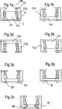
Unterhalb der Membran bildet der zwischen Membran und Unterseite des Gehäuses eingeschlossene und der Ausnehmung des MEMS-Chips entsprechende Raum ein erstes Teilvolumen TV1 des als Rückvolumen fungierenden Gesamtvolumens. Ein zweites Teilvolumen TV2 wird durch den Raum zur Verfügung gestellt, der seitlich des MEMS-Chips CH zwischen diesem und dem Gehäuse G verbleibt.Below the membrane, the space enclosed between the membrane and the underside of the housing and corresponding to the recess of the MEMS chip forms a first partial volume TV1 of the total volume acting as a back volume. A second subvolume TV2 is provided by the space remaining on the side of the MEMS chip CH between it and the housing G.
Um als gemeinsames Rückvolumen zu dienen, sind die beiden Teilvolumen TV1 und TV2 über einen oder mehrere Durchlässe verbunden, die beispielsweise in der Unterseite des MEMS-Chips vorgebildet sind oder zwischen Unterseite des MEMS-Chips und Gehäuse G verbleiben.In order to serve as a common back volume, the two sub-volumes TV1 and TV2 are connected via one or more passages, which are preformed for example in the lower side of the MEMS chip or remain between the lower side of the MEMS chip and the housing G.
Durch den innen über der Schalleintrittsöffnung OE aufsitzenden MEMS-Chips ist das zweite Teilvolumen TV2 gegen die Schalleintrittsöffnung OE abgedichtet. Dies kann durch eine Dichtmasse erfolgen, die beispielsweise ringförmig auf der Oberseite des MEMS-Chips aufgebracht ist und diesen gegen die obere Innenseite des Gehäuses G abdichtet.The second subvolume TV2 is sealed off from the sound inlet opening OE by the MEMS chips which are seated on the inside above the sound inlet opening OE. This can be done by a sealant, which is applied, for example, annular on the top of the MEMS chip and this seals against the upper inside of the housing G.
In einer nicht dargestellten Variante von
In der Variante gemäß
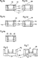
In
In
In
In
Die Verbindungsschicht VS ist vorzugsweise eine elastische Schicht und insbesondere eine elastische Kleberschicht, die einen ausreichend dichten Verschluss des Gehäuses durch die Abdeckung und insbesondere einen Verschluss des zweiten Teilvolumens TV2 gegen die Schalleintrittsöffnung ermöglicht. Die Verbindungsschicht VS kann großflächig auf der Unterseite der Abdeckung AB in den Bereich aufgebracht werden, der nicht dem Öffnungsbereich OB entspricht. Möglich ist es jedoch auch, die Verbindungsschicht VS ausschließlich an den Fügestellen zwischen Abdeckung und Unterteil entweder auf das Unterteil UT oder auf die Abdeckung AB aufzubringen.The connecting layer VS is preferably an elastic layer and in particular an elastic adhesive layer which allows a sufficiently tight closure of the housing by the cover and in particular a closure of the second partial volume TV2 against the sound inlet opening. The connecting layer VS can be applied over a large area on the underside of the cover AB in the area which does not correspond to the opening area OB. However, it is also possible to apply the bonding layer VS exclusively at the joints between the cover and the lower part, either on the lower part UT or on the cover AB.
Rahmenstruktur RS und Basisplatte BP können aus gleichen oder unterschiedlichen Materialien gefertigt sein. Vorteilhaft ist die Basisplatte eine Leiterplatte, auf die eine Rahmenstruktur aufgebracht wird, beispielsweise durch Aufdrucken, Fotostrukturieren oder galvanische Abscheidung oder eine beliebige andere zur Strukturerzeugung geeignete Methode.Frame structure RS and base plate BP may be made of the same or different materials. Advantageously, the base plate is a printed circuit board to which a frame structure is applied, for example by printing, photo-structuring or electrodeposition or any other method suitable for producing a structure.
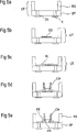
Im nächsten Schritt wird im Inneren des Unterteils eine Opferschicht OS aufgebracht und strukturiert. Es ist ausreichend, wenn bei der Strukturierung der Opferschicht die Anschlüsse am Boden des Unterteils freigelegt werden.
Im nächsten Schritt wird im Inneren des Unterteils eine Metallisierung aufgebracht und so strukturiert, dass Metallstrukturen MS elektrisch voneinander getrennt jeweils mit einem Anschluss verbunden und mit einem anderen Strukturbereich auf der Oberfläche der strukturierten Opferschicht OS zu liegen kommen. Die Metallstrukturen MS können sich dabei linear erstrecken, sind vorteilhaft jedoch gebogen oder gegebenenfalls mehrfach abgewinkelt, um eine spätere elastische Verformbarkeit der daraus hergestellten Federelemente in mehrere Raumrichtungen zu gewährleisten. Möglich ist es auch, die Metallstrukturen MS als brückenartige Strukturen auszuführen, bei denen ein erstes und ein zweites Ende direkt auf der Bodenplatte oder einem Anschluss im Inneren des Unterteils aufliegen, dazwischen jedoch ein mittlerer Bereich über die Opferschicht OS verläuft.
Im nächsten Schritt wird ein MEMS-Chip in das Unterteil UT eingesetzt und elektrisch leitend mit den Metallstrukturen MS verbunden. Dies kann durch Löten, Bonden, Verschweißen oder Kleben erfolgen.
Im nächsten Schritt wird die strukturierte Opferschicht OS entfernt, sodass die auf der Opferschicht aufliegenden Teile der Metallstruktur in einem lichten Abstand zur Oberseite der Bodenplatte BP verbleiben, sich also ein Freiraum FR zwischen den höher angeordneten Abschnitten der Metallstruktur und der Bodenplatte ergibt.In the next step, the structured sacrificial layer OS is removed so that the parts of the metal structure resting on the sacrificial layer remain at a clear distance from the top side of the bottom plate BP, thus resulting in a free space FR between the higher-positioned sections of the metal structure and the bottom plate.
Das Entfernen der Opferschicht kann auf eine geeignete Weise erfolgen, die dem Material der Opferschicht angepasst ist.The removal of the sacrificial layer can be done in a suitable manner, which is adapted to the material of the sacrificial layer.
Eine besonders einfache Ausführung verwendet ein thermisch zersetzbares Material, insbesondere ein bereits bei mäßigen Temperaturen von z. B. unter 300°C zersetzliches Polymer, welches in einem thermischen Schritt vollständig in gasförmige Zersetzungsprodukte überführt werden kann. Möglich ist es jedoch auch, die Opferschicht OS in einem selektiven Prozess in einer flüssigen Phase aufzulösen und so zu entfernen.
Prinzipiell ist es jedoch auch möglich, die Opferschicht direkt nach dem Herstellen der Metallstrukturen MS zu entfernen, da das elektrische und mechanische Verbinden des MEMS-Chips mit den nach Entfernen der Opferschicht zu den Federelementen FE gewordenen Metallstrukturen in einfache Weise möglich ist, in dem die Federelemente beim Aufsetzen, Aufbonden oder Aufkleben beliebig gegen die Oberseite der Basisplatte BP gedrückt werden können, ohne dass dabei die Federfunktion der Federelemente verloren geht, und die Federkraft daher zur Wiederherstellung der ursprünglichen Anordnung mit dem Freiraum FR führt.In principle, however, it is also possible to remove the sacrificial layer directly after the metal structures M S have been produced , since the electrical and mechanical connection of the MEMS chip to the metal structures that have become the spring elements FE after removal of the sacrificial layer is possible in a simple manner the spring elements can be pressed arbitrarily against the top of the base plate BP during placement, bonding or gluing, without losing the spring function of the spring elements, and the spring force therefore leads to the restoration of the original arrangement with the free space FR.
Eine beispielhafte Metallisierung M, die zur Herstellung sowohl der Innenmetallisierung MI, der Rahmenmetallisierung MR und der Metallstrukturen MS geeignet ist, kann wie folgt hergestellt werden. Zunächst wird ganzflächig auf den zu beschichtenden Oberflächen eine Haftschicht aufgebracht, die beispielsweise aus 50 Nanometer Ti und 200 Nanometer Cu besteht, beispielsweise durch Sputtern. Darüber wird zur Strukturierung anschließend ein Fotoresist aufgebracht, beispielsweise mittels Spray Coating oder durch Auflaminieren eines Trockenresistfilms. Der Fotolack oder Trockenresistfilm folgt dabei der Topographie der Ausnehmung und der Opferschicht. Dies kann zum Beispiel durch Vakuumlamination erreicht werden, die ein Aufbringen ohne Hohlräume unterstützt.An exemplary metallization M, which is suitable for producing both the inner metallization M I , the frame metallization MR and the metal structures M S , can be produced as follows. First, an adhesive layer is applied over the entire surface of the surfaces to be coated, which consists for example of 50 nanometers Ti and 200 nanometers Cu, for example by sputtering. In addition, a photoresist is subsequently applied for structuring, for example by means of spray coating or by lamination of a dry resist film. The photoresist or dry resist film follows the topography of the recess and the sacrificial layer. This can be achieved, for example, by vacuum lamination, which assists in application without cavities.
Die Belichtung des Fotoresists kann mit Masken erfolgen. Großflächige, nicht verzugsfreie Basisplatten, wie beispielsweise Basisplatten aus Keramik können auch mittels einer scannenden Vorrichtung und insbesondere mit einem Laserbelichter belichtet werden. Besonders vorteilhaft wird ein negativ arbeitender Fotoresist eingesetzt, da dann die senkrechte Flanke, also die Innenwand der Rahmenstruktur RS nicht belichtet zu werden braucht. Es kann auf diese Weise eine Resiststruktur erzeugt werden, die unbedeckte Bereiche der weiteren Metallabscheidung in einem galvanischen Verfahren zugänglich macht. Über eine Belichtung mittels Laser ist es jedoch auch möglich, Resiststruktur und Metallstrukturen auf beliebig geneigten Innenwänden aufzubringen.The exposure of the photoresist can be done with masks. Large-area, non-distortion-free base plates, such as base plates made of ceramic can also be exposed by means of a scanning device and in particular with a laser imager. Particularly advantageous is a negative-working photoresist is used, since then the vertical edge, so the inner wall of the frame structure RS need not be exposed. In this way it is possible to produce a resist structure which makes uncovered areas of the further metal deposition accessible in a galvanic process. However, laser exposure also makes it possible to apply resist structures and metal structures on arbitrarily inclined inner walls.
Im anschließenden Galvanikprozess werden Metallstrukturen MS, Innenmetallisierung MI und Rahmenmetallisierung MR galvanisch auf die nicht vom Fotoresist bedeckten Bereiche abgeschieden. Vorzugsweise werden in diesem Prozess Kupfer, Nickel oder Chrom in einer Dicke bis insgesamt zwei bis 50 μm abgeschieden. Die Metallisierung kann darüber hinaus weitere selektiv aufgetragene Schichten umfassen, die zum Beispiel dem Oxidationsschutz (mittels einer Gold- oder Palladiumschicht), der Bondbarkeit (zum Beispiel mittels einer Nickel- oder Goldschicht), der Lotbenetzung (zum Beispiel mittels einer Gold-, Palladium- oder Silberschicht) oder der Lotentnetzung (zum Beispiel mittels einer Titan-, Chrom- oder Aluminiumschicht) dienen. Diese weiteren Schichten können vor oder nach dem Entfernen der Resiststruktur erzeugt werden.In the subsequent electroplating process, metal structures M S , inner metallization M I and frame metallization MR are deposited galvanically on the areas not covered by the photoresist. Preferably, in this process, copper, nickel or chromium in a thickness of a total of two to 50 microns are deposited. The metallization may further comprise other selectively applied layers, for example, the oxidation protection (by means of a gold or palladium layer), the bondability (for example by means of a nickel or gold layer), the solder wetting (for example by means of a gold, palladium) or silver layer) or Lotentnetzung (for example by means of a titanium, chromium or aluminum layer) are used. These further layers can be produced before or after removal of the resist pattern.
Das Aufsetzen des MEMS-Chips beziehungsweise das elektrische und mechanische Verbinden kann über Goldstudbumps im Thermosonic-Bondverfahren auf die Metallstrukturen MS oder die frei gelegten Federelemente FE erfolgen. Bei galvanischer Erzeugung der verschiedenen Metallisierungen wird im letzten Schritt nach dem Entfernen der Opferschicht die dünne freiliegende Haftschicht ebenfalls weggeätzt.The placement of the MEMS chip or the electrical and mechanical connection can take place via gold Studbumps in the thermosonic bonding process on the metal structures M S or the exposed spring elements FE. When the various metallizations are galvanically produced, in the last step after the removal of the sacrificial layer, the thin, exposed adhesive layer is likewise etched away.
Zur Herstellung der Metallisierungen sind zahlreiche Varianten möglich. So können die Metallstrukturen auch durch Strukturierung großflächig aufgebrachter Metallschichten herausgeätzt werden. Möglich ist es auch, für Metallbeschichtung vorzusehende Bereiche insbesondere auf Kunststoffoberflächen zu aktivieren und anschließend eine nasschemische Metallisierung vorzunehmen. Dazu bietet sich die MID-(Molded Interconnect Device)Technik an.Numerous variants are possible for the production of the metallizations. Thus, the metal structures can also be etched out by structuring large-area applied metal layers. It is also possible to activate areas to be provided for metal coating, in particular on plastic surfaces, and then to carry out a wet-chemical metallization. The MID (Molded Interconnect Device) technology is ideal for this.
Für alle Ausführungsformen gilt, dass die Größenbemessung des Gehäuses so erfolgt, dass ein ausreichend großes Rückvolumen zur Verfügung steht. Für Ausführungsformen mit oben liegender Schalleintrittsöffnung ist die Größe so gewählt, dass mindestens 75 Prozent des nicht von dem MEMS-Chip verdrängten Innenvolumens als akustisches Rückvolumen verfügbar sind.For all embodiments, the size of the housing is made so that a sufficiently large back volume is available. For embodiments having a top sound inlet, the size is selected so that at least 75 percent of the interior volume not displaced by the MEMS chip is available as an acoustic return volume.
Mit der Erfindung wird ein gekapseltes MEMS-Mikrofon angegeben, welches bei minimaler Bauhöhe ein optimiertes Rückvolumen für die akustische Mikrofonfunktion garantiert. Auch die Grundfläche des Gehäuses ist minimiert und kleiner als bekannte Ausführungsformen gekapselter MEMS-Mikrofon-Chips.With the invention, an encapsulated MEMS microphone is specified, which guarantees an optimized back volume for the acoustic microphone function with minimal overall height. The base area of the housing is also minimized and smaller than known embodiments of encapsulated MEMS microphone chips.
Mit dem vorgeschlagenen Bauelement und dem Herstellungsverfahren gelingt es auch, den MEMS-Chips CH stressfrei in das Gehäuse G einzubauen, was auch bei mechanischer oder Temperaturwechselbelastung des Bauelements eine weitgehend ungestörte Mikrofonfunktion gewährleistet. Das Gehäuse kann bezüglich der dafür verwendeten Materialien und dem genauen geometrischen Aufbau beliebig variiert werden. Für Unterteil, Rahmenstruktur und Abdeckung können gleiche oder unterschiedliche Materialien eingesetzt werden. Vorzugsweise umfasst zumindest die Bodenplatte aber ein Schicht eines dielektrischen Materials, um die unterschiedlichen Anschlüsse und SMT-Kontakte gegeneinander zu isolieren.With the proposed device and the manufacturing method, it is also possible to install the MEMS chip CH stress-free in the housing G, which ensures a largely undisturbed microphone function even with mechanical or thermal cycling of the device. The housing can be varied as desired with respect to the materials used and the exact geometric structure. For base, frame structure and cover same or different materials can be used. Preferably, however, at least the bottom plate comprises a layer of dielectric material to isolate the different terminals and SMT contacts from one another.
Für das Bauelement können beliebige MEMS-Chips mit Mikrofonfunktion eingesetzt werden, die gegebenenfalls nach unterschiedlichen Prinzipien funktionieren. Bevorzugt werden MEMS-Chips mit Membran eingesetzt. Prinzipiell ist es jedoch auch möglich, MEMS-Chip mit anders aufgebauter beziehungsweise realisierter Mikrofonfunktion zu verwenden. Diejenigen mit Membran und über einer Ausnehmung können wie dargestellt eine konische Ausnehmung aufweisen, die aufgrund kristallachsenorientierter Ätzung oder überhaupt infolge isotroper Ätzung automatisch entstehen. Prinzipiell sind natürlich auch Ausnehmungen mit vertikalen oder anders ausgebildeten Seitenwänden für MEMS-Chips geeignet, was bezüglich eingesparter Grundfläche eine weitere Reduzierung des Flächenbedarfs des Bauelements ermöglicht.For the device any MEMS chips with microphone function can be used, which may function according to different principles. Preference is given to using MEMS chips with membrane. In principle, however, it is also possible to use a MEMS chip with a differently constructed or realized microphone function. Those with a membrane and over a recess can, as shown, have a conical recess which arises automatically due to crystal axis-oriented etching or even as a result of isotropic etching. In principle, recesses with vertical or differently formed side walls are of course also suitable for MEMS chips, which, with respect to the saved base area, enables a further reduction of the area required by the component.
Claims (27)
Priority Applications (4)
| Application Number | Priority Date | Filing Date | Title |
|---|---|---|---|
| DE102006046292.0A DE102006046292B9 (en) | 2006-09-29 | 2006-09-29 | Component with MEMS microphone and method of manufacture |
| PCT/DE2007/001754 WO2008040326A1 (en) | 2006-09-29 | 2007-09-27 | Component comprising a mems microphone and method for the production of said component |
| JP2009529532A JP4981913B2 (en) | 2006-09-29 | 2007-09-27 | Device having MEMS microphone and method for manufacturing the device |
| US12/409,328 US8218794B2 (en) | 2006-09-29 | 2009-03-23 | Component comprising a MEMS microphone and method for the production of said component |
Applications Claiming Priority (1)
| Application Number | Priority Date | Filing Date | Title |
|---|---|---|---|
| DE102006046292.0A DE102006046292B9 (en) | 2006-09-29 | 2006-09-29 | Component with MEMS microphone and method of manufacture |
Publications (3)
| Publication Number | Publication Date |
|---|---|
| DE102006046292A1 DE102006046292A1 (en) | 2008-04-03 |
| DE102006046292B4 true DE102006046292B4 (en) | 2014-01-16 |
| DE102006046292B9 DE102006046292B9 (en) | 2014-04-30 |
Family
ID=38863065
Family Applications (1)
| Application Number | Title | Priority Date | Filing Date |
|---|---|---|---|
| DE102006046292.0A Active DE102006046292B9 (en) | 2006-09-29 | 2006-09-29 | Component with MEMS microphone and method of manufacture |
Country Status (4)
| Country | Link |
|---|---|
| US (1) | US8218794B2 (en) |
| JP (1) | JP4981913B2 (en) |
| DE (1) | DE102006046292B9 (en) |
| WO (1) | WO2008040326A1 (en) |
Families Citing this family (51)
| Publication number | Priority date | Publication date | Assignee | Title |
|---|---|---|---|---|
| GB0605576D0 (en) * | 2006-03-20 | 2006-04-26 | Oligon Ltd | MEMS device |
| DE102008005686B9 (en) | 2008-01-23 | 2019-06-27 | Tdk Corporation | MEMS device and method for manufacturing a MEMS device |
| US8259968B2 (en) * | 2008-04-28 | 2012-09-04 | Tsinghua University | Thermoacoustic device |
| US8259967B2 (en) * | 2008-04-28 | 2012-09-04 | Tsinghua University | Thermoacoustic device |
| US8270639B2 (en) * | 2008-04-28 | 2012-09-18 | Tsinghua University | Thermoacoustic device |
| US8452031B2 (en) * | 2008-04-28 | 2013-05-28 | Tsinghua University | Ultrasonic thermoacoustic device |
| DE102008032319B4 (en) * | 2008-07-09 | 2012-06-06 | Epcos Ag | Method for producing an MST component |
| CN101715160B (en) * | 2008-10-08 | 2013-02-13 | 清华大学 | Flexible sound producing device and sound producing flag |
| CN101771922B (en) * | 2008-12-30 | 2013-04-24 | 清华大学 | Sounding device |
| US8325947B2 (en) * | 2008-12-30 | 2012-12-04 | Bejing FUNATE Innovation Technology Co., Ltd. | Thermoacoustic device |
| US8300855B2 (en) * | 2008-12-30 | 2012-10-30 | Beijing Funate Innovation Technology Co., Ltd. | Thermoacoustic module, thermoacoustic device, and method for making the same |
| JP5045769B2 (en) | 2009-03-04 | 2012-10-10 | 株式会社デンソー | Manufacturing method of sensor device |
| CN101922755A (en) * | 2009-06-09 | 2010-12-22 | 清华大学 | Heating wall |
| CN101943850B (en) * | 2009-07-03 | 2013-04-24 | 清华大学 | Sound-producing screen and projection system using same |
| JP5404220B2 (en) * | 2009-07-09 | 2014-01-29 | 株式会社オーディオテクニカ | Condenser microphone |
| CN101990152B (en) * | 2009-08-07 | 2013-08-28 | 清华大学 | Thermal sounding device and manufacturing method thereof |
| CN102006542B (en) | 2009-08-28 | 2014-03-26 | 清华大学 | Sound generating device |
| CN102023297B (en) * | 2009-09-11 | 2015-01-21 | 清华大学 | Sonar system |
| CN102034467B (en) * | 2009-09-25 | 2013-01-30 | 北京富纳特创新科技有限公司 | Sound production device |
| CN102056064B (en) * | 2009-11-06 | 2013-11-06 | 清华大学 | Loudspeaker |
| CN102056065B (en) * | 2009-11-10 | 2014-11-12 | 北京富纳特创新科技有限公司 | Sound production device |
| CN102065363B (en) * | 2009-11-16 | 2013-11-13 | 北京富纳特创新科技有限公司 | Sound production device |
| US11175279B2 (en) | 2010-05-03 | 2021-11-16 | Creatv Microtech, Inc. | Polymer microfilters, devices comprising the same, methods of manufacturing the same, and uses thereof |
| US8901736B2 (en) | 2010-05-28 | 2014-12-02 | Taiwan Semiconductor Manufacturing Company, Ltd. | Strength of micro-bump joints |
| DE102010026519B4 (en) * | 2010-07-08 | 2016-03-10 | Epcos Ag | Case with MEMS microphone, electrical device with housing with MEMS microphone and method of manufacture |
| WO2012004339A1 (en) | 2010-07-08 | 2012-01-12 | Epcos Ag | Mems microphone and method for producing the mems microphone |
| JP2012039272A (en) * | 2010-08-05 | 2012-02-23 | Funai Electric Co Ltd | Microphone unit |
| DE102011087963A1 (en) | 2010-12-14 | 2012-06-14 | Robert Bosch Gmbh | Microphone package, has housing cover connected with housing bottom by connection material that has low hardening temperature and/or requires short time for curing than another connection material connecting cover with microphone chip |
| DE102010054782A1 (en) * | 2010-12-16 | 2012-06-21 | Epcos Ag | Housing electrical component |
| US10195570B2 (en) * | 2011-01-07 | 2019-02-05 | Creative Micro Tech, Inc. | Fabrication of microfilters and nanofilters and their applications |
| US8824706B2 (en) * | 2011-08-30 | 2014-09-02 | Qualcomm Mems Technologies, Inc. | Piezoelectric microphone fabricated on glass |
| US8913180B2 (en) * | 2011-09-29 | 2014-12-16 | Flextronics Ap, Llc | Folded tape package for electronic devices |
| US20130147040A1 (en) * | 2011-12-09 | 2013-06-13 | Robert Bosch Gmbh | Mems chip scale package |
| US20140064546A1 (en) * | 2012-08-01 | 2014-03-06 | Knowles Electronics, Llc | Microphone assembly |
| US9181086B1 (en) | 2012-10-01 | 2015-11-10 | The Research Foundation For The State University Of New York | Hinged MEMS diaphragm and method of manufacture therof |
| US8965027B2 (en) * | 2013-02-15 | 2015-02-24 | Invensense, Inc. | Packaged microphone with frame having die mounting concavity |
| ITTO20130247A1 (en) * | 2013-03-26 | 2014-09-27 | St Microelectronics Srl | METHOD OF ENCAPSULATION OF A MEMS TRANSDUCER DEVICE AND ENCAPSULATED MEMS TRANSDUCER DEVICE |
| DE102013106353B4 (en) * | 2013-06-18 | 2018-06-28 | Tdk Corporation | Method for applying a structured coating to a component |
| DE102014106220B4 (en) * | 2014-05-05 | 2020-06-18 | Tdk Corporation | Sensor component with two sensor functions |
| DE102014106503B4 (en) * | 2014-05-08 | 2016-03-03 | Epcos Ag | Method of making a microphone |
| DE102014106818B3 (en) * | 2014-05-14 | 2015-11-12 | Epcos Ag | microphone |
| DE102014211188A1 (en) * | 2014-06-12 | 2015-12-17 | Robert Bosch Gmbh | Vertical hybrid integrated component with interposer for stress decoupling of a MEMS structure and method for its production |
| TW201612678A (en) * | 2014-09-26 | 2016-04-01 | 3R Semiconductor Technology Inc | Electronic device with dust protecting function and method for fabricating electronic device with dust protecting function |
| US20160297671A1 (en) * | 2015-04-13 | 2016-10-13 | Epcos Ag | MEMS Sensor Component |
| DE102015112642A1 (en) * | 2015-07-31 | 2017-02-02 | Epcos Ag | Microphone in top port design and manufacturing process |
| US20170240418A1 (en) * | 2016-02-18 | 2017-08-24 | Knowles Electronics, Llc | Low-cost miniature mems vibration sensor |
| US9745188B1 (en) * | 2016-02-26 | 2017-08-29 | Infineon Technologies Ag | Microelectromechanical device and method for forming a microelectromechanical device |
| US9856134B2 (en) | 2016-02-26 | 2018-01-02 | Infineon Technologies Ag | Microelectromechanical system and a method of manufacturing a microelectromechanical system |
| US10773949B2 (en) | 2016-03-14 | 2020-09-15 | At&S Austria Technologie & Systemtechnik Aktiengesellschaft | Method of manufacturing an electronic device |
| JP6771837B2 (en) * | 2016-07-07 | 2020-10-21 | モレックス エルエルシー | Molded interconnect device and its manufacturing method |
| DE102016124057A1 (en) * | 2016-12-12 | 2018-06-14 | Epcos Ag | MEMS microphone with top sound opening and reduced mechanical stress and manufacturing process |
Citations (6)
| Publication number | Priority date | Publication date | Assignee | Title |
|---|---|---|---|---|
| US6396711B1 (en) * | 2000-06-06 | 2002-05-28 | Agere Systems Guardian Corp. | Interconnecting micromechanical devices |
| US20030230798A1 (en) * | 2002-06-12 | 2003-12-18 | Jong-Kai Lin | Wafer level MEMS packaging |
| US20050185812A1 (en) * | 2000-11-28 | 2005-08-25 | Knowles Electronics, Llc | Miniature silicon condenser microphone and method for producing the same |
| US20050189635A1 (en) * | 2004-03-01 | 2005-09-01 | Tessera, Inc. | Packaged acoustic and electromagnetic transducer chips |
| WO2006085825A1 (en) * | 2005-02-08 | 2006-08-17 | Altus Technologies Pte. Ltd. | A packaging method for mems devices, and mems packages produced using the method |
| DE102005008512A1 (en) * | 2005-02-24 | 2006-08-31 | Epcos Ag | Electrical module, has base plate with acoustic channel whose one end opens out into cavity, where channel is separated from another cavity by diaphragm of microphone chip which closes other end of channel |
Family Cites Families (11)
| Publication number | Priority date | Publication date | Assignee | Title |
|---|---|---|---|---|
| JPS51131315A (en) * | 1975-05-10 | 1976-11-15 | Hitachi Zosen Corp | Microphone |
| JPH02149199A (en) * | 1988-11-30 | 1990-06-07 | Matsushita Electric Ind Co Ltd | Electlet condenser microphone |
| US5573679A (en) * | 1995-06-19 | 1996-11-12 | Alberta Microelectronic Centre | Fabrication of a surface micromachined capacitive microphone using a dry-etch process |
| US7434305B2 (en) * | 2000-11-28 | 2008-10-14 | Knowles Electronics, Llc. | Method of manufacturing a microphone |
| US6686642B2 (en) * | 2001-06-11 | 2004-02-03 | Hewlett-Packard Development Company, L.P. | Multi-level integrated circuit for wide-gap substrate bonding |
| JP3926701B2 (en) * | 2002-08-06 | 2007-06-06 | ホシデン株式会社 | Manufacturing method of vibrating membrane for electrostatic electroacoustic transducer |
| US6946742B2 (en) * | 2002-12-19 | 2005-09-20 | Analog Devices, Inc. | Packaged microchip with isolator having selected modulus of elasticity |
| US6932187B2 (en) * | 2003-10-14 | 2005-08-23 | Gore Enterprise Holdings, Inc. | Protective acoustic cover assembly |
| DE102004011149B3 (en) * | 2004-03-08 | 2005-11-10 | Infineon Technologies Ag | Microphone and method of making a microphone |
| JP2006153804A (en) * | 2004-12-01 | 2006-06-15 | Alps Electric Co Ltd | Pressure sensor |
| DE102005053767B4 (en) * | 2005-11-10 | 2014-10-30 | Epcos Ag | MEMS microphone, method of manufacture and method of installation |
-
2006
- 2006-09-29 DE DE102006046292.0A patent/DE102006046292B9/en active Active
-
2007
- 2007-09-27 JP JP2009529532A patent/JP4981913B2/en not_active Expired - Fee Related
- 2007-09-27 WO PCT/DE2007/001754 patent/WO2008040326A1/en active Application Filing
-
2009
- 2009-03-23 US US12/409,328 patent/US8218794B2/en active Active
Patent Citations (6)
| Publication number | Priority date | Publication date | Assignee | Title |
|---|---|---|---|---|
| US6396711B1 (en) * | 2000-06-06 | 2002-05-28 | Agere Systems Guardian Corp. | Interconnecting micromechanical devices |
| US20050185812A1 (en) * | 2000-11-28 | 2005-08-25 | Knowles Electronics, Llc | Miniature silicon condenser microphone and method for producing the same |
| US20030230798A1 (en) * | 2002-06-12 | 2003-12-18 | Jong-Kai Lin | Wafer level MEMS packaging |
| US20050189635A1 (en) * | 2004-03-01 | 2005-09-01 | Tessera, Inc. | Packaged acoustic and electromagnetic transducer chips |
| WO2006085825A1 (en) * | 2005-02-08 | 2006-08-17 | Altus Technologies Pte. Ltd. | A packaging method for mems devices, and mems packages produced using the method |
| DE102005008512A1 (en) * | 2005-02-24 | 2006-08-31 | Epcos Ag | Electrical module, has base plate with acoustic channel whose one end opens out into cavity, where channel is separated from another cavity by diaphragm of microphone chip which closes other end of channel |
Also Published As
| Publication number | Publication date |
|---|---|
| DE102006046292A1 (en) | 2008-04-03 |
| WO2008040326A1 (en) | 2008-04-10 |
| JP4981913B2 (en) | 2012-07-25 |
| US20090232336A1 (en) | 2009-09-17 |
| US8218794B2 (en) | 2012-07-10 |
| JP2010505304A (en) | 2010-02-18 |
| DE102006046292B9 (en) | 2014-04-30 |
Similar Documents
| Publication | Publication Date | Title |
|---|---|---|
| DE102006046292B4 (en) | Component with MEMS microphone and method of manufacture | |
| DE102005053767B4 (en) | MEMS microphone, method of manufacture and method of installation | |
| DE102007058951B4 (en) | MEMS package | |
| DE102005008512B4 (en) | Electrical module with a MEMS microphone | |
| DE102005053765B4 (en) | MEMS package and method of manufacture | |
| DE102004005668B4 (en) | Electrical component and manufacturing process | |
| WO2010089261A2 (en) | Sensor module and method for producing sensor modules | |
| DE102010052071A1 (en) | Housing systems of microsystem technology microphones | |
| WO2012004339A1 (en) | Mems microphone and method for producing the mems microphone | |
| WO2011092137A2 (en) | Miniaturized electrical component comprising an mems and an asic and production method | |
| WO2003067657A2 (en) | Semiconductor component comprising a sensor surface or an actuator surface, and method for producing the same | |
| WO2012079927A1 (en) | Cased electrical component | |
| WO2008025725A1 (en) | Hermetic sealing and electrical contacting of a microelectromechanical structure, and microsystem (mems) produced therewith | |
| DE10144467B4 (en) | Electronic sensor component and method for its production | |
| EP2313338A2 (en) | Process for manufacturing a component, process for manufacturing a component arrangement, component and component arrangement | |
| DE102017220258B4 (en) | Semiconductor sensor device and method for producing the same | |
| DE102011012295B4 (en) | MEMS microphone and method for manufacturing the MEMS microphone | |
| DE10141571B4 (en) | A method of assembling a semiconductor device and integrated circuit fabricated therewith that is suitable for three-dimensional, multi-layered circuits | |
| DE10331322A1 (en) | Electronic component and method of manufacture | |
| DE10246101A1 (en) | Method for producing a housing for a chip with a micromechanical structure | |
| DE102005063640B3 (en) | MEMS package and method of manufacture | |
| DE102017208628B4 (en) | METHOD OF MAKING AN ELECTRICAL CONNECTION | |
| DE10256945A1 (en) | Multi-chip electronic device and method of manufacture | |
| DE102018203101A1 (en) | HOUSED SEMICONDUCTOR DEVICES AND METHOD FOR PRODUCING HOUSED SEMICONDUCTOR DEVICES | |
| DE102012220323A1 (en) | Component and method for its production |
Legal Events
| Date | Code | Title | Description |
|---|---|---|---|
| OP8 | Request for examination as to paragraph 44 patent law | ||
| R016 | Response to examination communication | ||
| R016 | Response to examination communication | ||
| R018 | Grant decision by examination section/examining division | ||
| R083 | Amendment of/additions to inventor(s) | ||
| R020 | Patent grant now final | ||
| R020 | Patent grant now final |
Effective date: 20141017 |
|
| R081 | Change of applicant/patentee |
Owner name: TDK CORPORATION, JP Free format text: FORMER OWNER: EPCOS AG, 81669 MUENCHEN, DE |
|
| R082 | Change of representative |
Representative=s name: EPPING HERMANN FISCHER, PATENTANWALTSGESELLSCH, DE Representative=s name: EPPING HERMANN FISCHER PATENTANWALTSGESELLSCHA, DE |