CN1591152A - Liquid crystal display and thin film transistor array panel therefor - Google Patents
Liquid crystal display and thin film transistor array panel therefor Download PDFInfo
- Publication number
- CN1591152A CN1591152A CNA2004100794360A CN200410079436A CN1591152A CN 1591152 A CN1591152 A CN 1591152A CN A2004100794360 A CNA2004100794360 A CN A2004100794360A CN 200410079436 A CN200410079436 A CN 200410079436A CN 1591152 A CN1591152 A CN 1591152A
- Authority
- CN
- China
- Prior art keywords
- electrode
- film transistor
- data line
- lcd
- pixel electrode
- Prior art date
- Legal status (The legal status is an assumption and is not a legal conclusion. Google has not performed a legal analysis and makes no representation as to the accuracy of the status listed.)
- Pending
Links
Images


Classifications
-
- G—PHYSICS
- G02—OPTICS
- G02F—OPTICAL DEVICES OR ARRANGEMENTS FOR THE CONTROL OF LIGHT BY MODIFICATION OF THE OPTICAL PROPERTIES OF THE MEDIA OF THE ELEMENTS INVOLVED THEREIN; NON-LINEAR OPTICS; FREQUENCY-CHANGING OF LIGHT; OPTICAL LOGIC ELEMENTS; OPTICAL ANALOGUE/DIGITAL CONVERTERS
- G02F1/00—Devices or arrangements for the control of the intensity, colour, phase, polarisation or direction of light arriving from an independent light source, e.g. switching, gating or modulating; Non-linear optics
- G02F1/01—Devices or arrangements for the control of the intensity, colour, phase, polarisation or direction of light arriving from an independent light source, e.g. switching, gating or modulating; Non-linear optics for the control of the intensity, phase, polarisation or colour
- G02F1/13—Devices or arrangements for the control of the intensity, colour, phase, polarisation or direction of light arriving from an independent light source, e.g. switching, gating or modulating; Non-linear optics for the control of the intensity, phase, polarisation or colour based on liquid crystals, e.g. single liquid crystal display cells
- G02F1/133—Constructional arrangements; Operation of liquid crystal cells; Circuit arrangements
- G02F1/1333—Constructional arrangements; Manufacturing methods
- G02F1/1337—Surface-induced orientation of the liquid crystal molecules, e.g. by alignment layers
- G02F1/133707—Structures for producing distorted electric fields, e.g. bumps, protrusions, recesses, slits in pixel electrodes
-
- G—PHYSICS
- G02—OPTICS
- G02F—OPTICAL DEVICES OR ARRANGEMENTS FOR THE CONTROL OF LIGHT BY MODIFICATION OF THE OPTICAL PROPERTIES OF THE MEDIA OF THE ELEMENTS INVOLVED THEREIN; NON-LINEAR OPTICS; FREQUENCY-CHANGING OF LIGHT; OPTICAL LOGIC ELEMENTS; OPTICAL ANALOGUE/DIGITAL CONVERTERS
- G02F1/00—Devices or arrangements for the control of the intensity, colour, phase, polarisation or direction of light arriving from an independent light source, e.g. switching, gating or modulating; Non-linear optics
- G02F1/01—Devices or arrangements for the control of the intensity, colour, phase, polarisation or direction of light arriving from an independent light source, e.g. switching, gating or modulating; Non-linear optics for the control of the intensity, phase, polarisation or colour
- G02F1/13—Devices or arrangements for the control of the intensity, colour, phase, polarisation or direction of light arriving from an independent light source, e.g. switching, gating or modulating; Non-linear optics for the control of the intensity, phase, polarisation or colour based on liquid crystals, e.g. single liquid crystal display cells
- G02F1/133—Constructional arrangements; Operation of liquid crystal cells; Circuit arrangements
- G02F1/1333—Constructional arrangements; Manufacturing methods
- G02F1/1343—Electrodes
- G02F1/134309—Electrodes characterised by their geometrical arrangement
- G02F1/134336—Matrix
-
- G—PHYSICS
- G02—OPTICS
- G02F—OPTICAL DEVICES OR ARRANGEMENTS FOR THE CONTROL OF LIGHT BY MODIFICATION OF THE OPTICAL PROPERTIES OF THE MEDIA OF THE ELEMENTS INVOLVED THEREIN; NON-LINEAR OPTICS; FREQUENCY-CHANGING OF LIGHT; OPTICAL LOGIC ELEMENTS; OPTICAL ANALOGUE/DIGITAL CONVERTERS
- G02F1/00—Devices or arrangements for the control of the intensity, colour, phase, polarisation or direction of light arriving from an independent light source, e.g. switching, gating or modulating; Non-linear optics
- G02F1/01—Devices or arrangements for the control of the intensity, colour, phase, polarisation or direction of light arriving from an independent light source, e.g. switching, gating or modulating; Non-linear optics for the control of the intensity, phase, polarisation or colour
- G02F1/13—Devices or arrangements for the control of the intensity, colour, phase, polarisation or direction of light arriving from an independent light source, e.g. switching, gating or modulating; Non-linear optics for the control of the intensity, phase, polarisation or colour based on liquid crystals, e.g. single liquid crystal display cells
- G02F1/133—Constructional arrangements; Operation of liquid crystal cells; Circuit arrangements
- G02F1/1333—Constructional arrangements; Manufacturing methods
- G02F1/1343—Electrodes
- G02F1/134309—Electrodes characterised by their geometrical arrangement
- G02F1/134318—Electrodes characterised by their geometrical arrangement having a patterned common electrode
-
- G—PHYSICS
- G02—OPTICS
- G02F—OPTICAL DEVICES OR ARRANGEMENTS FOR THE CONTROL OF LIGHT BY MODIFICATION OF THE OPTICAL PROPERTIES OF THE MEDIA OF THE ELEMENTS INVOLVED THEREIN; NON-LINEAR OPTICS; FREQUENCY-CHANGING OF LIGHT; OPTICAL LOGIC ELEMENTS; OPTICAL ANALOGUE/DIGITAL CONVERTERS
- G02F1/00—Devices or arrangements for the control of the intensity, colour, phase, polarisation or direction of light arriving from an independent light source, e.g. switching, gating or modulating; Non-linear optics
- G02F1/01—Devices or arrangements for the control of the intensity, colour, phase, polarisation or direction of light arriving from an independent light source, e.g. switching, gating or modulating; Non-linear optics for the control of the intensity, phase, polarisation or colour
- G02F1/13—Devices or arrangements for the control of the intensity, colour, phase, polarisation or direction of light arriving from an independent light source, e.g. switching, gating or modulating; Non-linear optics for the control of the intensity, phase, polarisation or colour based on liquid crystals, e.g. single liquid crystal display cells
- G02F1/137—Devices or arrangements for the control of the intensity, colour, phase, polarisation or direction of light arriving from an independent light source, e.g. switching, gating or modulating; Non-linear optics for the control of the intensity, phase, polarisation or colour based on liquid crystals, e.g. single liquid crystal display cells characterised by the electro-optical or magneto-optical effect, e.g. field-induced phase transition, orientation effect, guest-host interaction or dynamic scattering
- G02F1/139—Devices or arrangements for the control of the intensity, colour, phase, polarisation or direction of light arriving from an independent light source, e.g. switching, gating or modulating; Non-linear optics for the control of the intensity, phase, polarisation or colour based on liquid crystals, e.g. single liquid crystal display cells characterised by the electro-optical or magneto-optical effect, e.g. field-induced phase transition, orientation effect, guest-host interaction or dynamic scattering based on orientation effects in which the liquid crystal remains transparent
- G02F1/1393—Devices or arrangements for the control of the intensity, colour, phase, polarisation or direction of light arriving from an independent light source, e.g. switching, gating or modulating; Non-linear optics for the control of the intensity, phase, polarisation or colour based on liquid crystals, e.g. single liquid crystal display cells characterised by the electro-optical or magneto-optical effect, e.g. field-induced phase transition, orientation effect, guest-host interaction or dynamic scattering based on orientation effects in which the liquid crystal remains transparent the birefringence of the liquid crystal being electrically controlled, e.g. ECB-, DAP-, HAN-, PI-LC cells
Landscapes
- Physics & Mathematics (AREA)
- Nonlinear Science (AREA)
- Mathematical Physics (AREA)
- Chemical & Material Sciences (AREA)
- Crystallography & Structural Chemistry (AREA)
- General Physics & Mathematics (AREA)
- Optics & Photonics (AREA)
- Spectroscopy & Molecular Physics (AREA)
- Geometry (AREA)
- Liquid Crystal (AREA)
- Devices For Indicating Variable Information By Combining Individual Elements (AREA)
Abstract
A liquid crystal display is provided, which includes a thin film transistor array panel and a common electrode panel facing the thin film transistor array panel. The thin film transistor array panel includes a first gate line; a data line intersecting the gate line; a first thin film transistor including a gate electrode connected to the gate line, a source electrode connected to the data line, and a drain electrode; a first pixel electrode connected to the drain electrode; and a capacitor electrode overlapping at least one of the pixel electrode and the drain electrode with interposing an insulator. The common electrode panel includes a common electrode that faces the pixel electrode and has an opening facing at least one of the drain electrode and the capacitor electrode.
Description
Technical field
The present invention relates to a kind of LCD and film transistor array plate thereof.
Background technology
LCD (LCD) is one of most widely used flat-panel monitor.LCD comprises liquid crystal (LC) layer that is clipped between a pair of plate that is provided with a generating electrodes.The LC layer is in the electric field that electrode produces, and field intensity changes the molecular orientation that can change the LC layer, and molecular orientation changes the polarisation of light by liquid crystal layer thereupon.Based on polarisation of light, suitably the polarizer that is provided with can change the optical transmission rate.
A detection index of LCD quality is the visual angle, and it is limited by the angle that LCD shows predetermined comparison degree place.Propose to enlarge the various technology at visual angle, comprised the LC layer that uses homeotropic alignment and in the technology that breach or projection are set as the generating electrodes place, field of pixel electrode and common electrode.
Yet breach and projection have reduced the aperture ratio.In order to improve the aperture ratio, proposed to make the maximization of pixel electrode size.But the maximization of pixel electrode size will cause the distance between pixel electrode too near, thereby produce very strong transverse electric field between pixel electrode.Highfield will cause the LC molecular orientation that the variation of not expecting takes place, and produce striped and light and will leak, and reduce display performance.Striped and light leak and can shield by the black matrix of broad, but this has reduced the aperture ratio equally.
Simultaneously, pixel electrode and common electrode form the capacitor that inserts liquid crystal layer, are called the LC capacitor, and pixel electrode and the signal wire that is provided with onboard form auxiliary capacitor, are called reservior capacitor, and reservior capacitor is in parallel with the LC capacitor.Electric capacity between LC capacitor and reservior capacitor has and is used for the suitable value and the proper proportion of fully charging to described capacitor.
Yet, because square being directly proportional of described LC electric capacity and pixel electrode spacing, so increase sharply with the increase of LCD and pixel electrode size.The increase of LC electric capacity has reduced the charge rate of LC capacitor, and has increased the response time of liquid crystal.Although the reduction of charge rate can remedy by increasing storage capacitors, the increase of response time can remedy by the width that increases breach or projection, and this will cause the reduction of aperture ratio.
Summary of the invention
An object of the present invention is to provide a kind of LCD with LC electric capacity of optimization.
Another object of the present invention provides a kind of LCD with enough apertures ratio.
Another purpose of the present invention provides a kind of LCD with stable liquid crystal arrangement.
A further object of the present invention provides a kind of dot structure of being convenient to be used for any LCD.
Provide a kind of LCD, the common electrode plate that it comprises film transistor array plate and faces film transistor array plate.This film transistor array plate comprises: first grid polar curve; With the crossing data line of this gate line; The first film transistor, it comprises the gate electrode that is connected with described gate line, the source electrode that is connected with described data line and drain electrode; First pixel electrode that is connected with described drain electrode; And with described pixel electrode and drain electrode in one of at least overlapping and accompany the electrode for capacitors of insulator.Described common electrode plate comprises in the face of described pixel electrode and has in the face of one of at least the common electrode of opening in described drain electrode and the electrode for capacitors.
Described data line can comprise sweep and the cross section that is connected with sweep and intersects with gate line.The sweep of data line can comprise a pair of straight line portion that is connected to each other and becomes about miter angle with gate line.Described pixel electrode can be along the sweep bending of data line.
Described pixel electrode can be overlapping with described data line at least in part.
This LCD also can comprise: with described first grid polar curve and data line separates and contiguous described first pixel electrode is provided with second grid line; Second thin film transistor (TFT) that is connected with the second grid line; And second pixel electrode that is connected with second thin film transistor (TFT).
Described electrode for capacitors can be connected with the second grid line, and this LCD also can comprise and described pixel electrode electrically connects and be arranged on capacitor conductor between described electrode for capacitors and the pixel electrode.
Certainly, described electrode for capacitors also can disconnect with the second grid line.
This LCD also can comprise the light filter on any one that is arranged on described film transistor array plate and common electrode plate.
This LCD also can comprise and places described film transistor array plate to use liquid crystal layer between the battery lead plate together.
This liquid crystal layer can have negative anisotropy and perpendicular is aimed at.This LCD also can comprise the inclination control assembly of vergence direction of molecule in this liquid crystal layer of control, and this inclination control assembly can be included in otch in described pixel electrode or the common electrode or the projection on described pixel electrode and the common electrode.
This LCD also can comprise and described gate electrode is oppositely arranged and comprise at described source electrode and the semiconductor layer of the first between draining.This semiconductor layer also can comprise the second portion that is arranged under the described data line.Except that described first, semiconductor layer can have and described data line, source electrode and the essentially identical planar graph that drains.
A kind of film transistor array plate is provided, and it comprises: substrate; Be formed in the substrate and comprise the gate line of gate electrode; Be formed in the substrate and comprise sweep and the data line of the cross section that intersects with described gate line; The thin film transistor (TFT) that comprises the gate electrode that is connected with described gate line, the source electrode that is connected with described data line and drain electrode; The pixel electrode that is connected with described drain electrode; And with described pixel electrode and drain electrode in one of at least overlapping and accompany the storage electrode of insulator, comprise one of at least the part of extending in wherein said drain electrode and the storage electrode along the sweep that is parallel to described data line.
The sweep of described data line comprises a pair of part that becomes the clockwise angle and the about 45 counterclockwise angles of spending of about 45 degree with respect to described gate line respectively.
Described drain electrode and storage electrode can overlap each other.
Described source electrode can be connected with the cross section of described data line.
Described pixel electrode can be along the sweep bending of described data line.
Described pixel electrode can be overlapping with described data line at least in part.
Between can comprising, described pixel electrode is provided with a pair of subregion (partitions) of otch.
This film transistor array plate also can comprise and described gate electrode is oppositely arranged and comprise at described source electrode and the semiconductor layer of the first between draining.This semiconductor layer also can comprise the second portion that is arranged under the described data line.Except that first, this semiconductor layer can have and described data line, source electrode and the essentially identical planar graph that drains.
Provide a kind of LCD, the common electrode plate that it comprises film transistor array plate and faces film transistor array plate.This film transistor array plate comprises: substrate; Be formed in the substrate and comprise the gate line of gate electrode; Be formed in the substrate and comprise sweep and the data line of the cross section that intersects with described gate line; The thin film transistor (TFT) that comprises the gate electrode that is connected with described gate line, the source electrode that is connected with described data line and drain electrode; The pixel electrode that is connected with described drain electrode; And with described pixel electrode and drain electrode in one of at least overlapping and accompany the storage electrode of insulator.Described common electrode plate comprises the common electrode in the face of described pixel electrode.
This LCD also can comprise the light filter on any one that is arranged on described film transistor array plate and common electrode plate.
This LCD also can comprise and places described film transistor array plate together with between the battery lead plate and have a liquid crystal layer that negative anisotropy and perpendicular are aimed at.This LCD also can comprise the inclination control assembly of the vergence direction of molecule in the described liquid crystal layer of control.Described inclination control assembly can be included in otch in described pixel electrode or the common electrode or the projection on pixel electrode or the common electrode.
Described inclination control assembly can be crooked abreast with described data line.This inclination control assembly can in the face of in described drain electrode and the storage electrode one of at least.
Description of drawings
Specifically describe embodiments of the present invention by the reference accompanying drawing and will make the present invention distincter, in the accompanying drawing:
Fig. 1 is the tft array plate arrangenent diagram that is used for LCD of an embodiment of the present invention;
Fig. 2 is the common electrode plate arrangenent diagram that is used for LCD of embodiment of the present invention;
Fig. 3 is the arrangenent diagram that comprises the LCD of tft array plate shown in Figure 1 and common electrode plate shown in Figure 2;
Fig. 4 is the sectional view that LCD IV-IV ' along the line shown in Figure 3 dissects;
Fig. 5 is LCD V-V ' along the line and V '-V shown in Figure 3 " sectional view that dissects;
Fig. 6 is the arrangenent diagram of tft array plate of the LCD of another embodiment of the present invention;
Fig. 7 is the sectional view that comprises that the LCD VII-VII ' along the line of tft array plate shown in Figure 6 dissects;
Fig. 8 is LCD VIII-VIII ' along the line and the VIII '-VIII that comprises tft array plate shown in Figure 6 " sectional view that dissects;
Fig. 9 is the arrangenent diagram of the LCD of the another embodiment of the present invention;
Figure 10 is the sectional view that LCD X-X ' along the line shown in Figure 9 dissects;
Figure 11 is the present invention's LCD arrangenent diagram of an embodiment again;
Figure 12 is the sectional view that LCD XII-XII ' along the line shown in Figure 11 dissects;
Figure 13 is the LCD arrangenent diagram of another embodiment of the present invention;
Figure 14 is the sectional view that LCD XIV-XIV ' along the line shown in Figure 13 dissects;
Figure 15 is LCD XV-XV ' along the line and XV '-XV shown in Figure 13 " sectional view that dissects;
Figure 16 is the LCD arrangenent diagram of the another embodiment of the present invention;
Figure 17 is the sectional view that the tft array plate XVII-XVII ' along the line of LCD shown in Figure 16 dissects;
Figure 18 is the present invention's tft array plate arrangenent diagram of the LCD of an embodiment again;
Figure 19 is the common electrode plate arrangenent diagram of the LCD of another embodiment of the present invention;
Figure 20 is the LCD arrangenent diagram that comprises tft array plate shown in Figure 180 and common electrode plate shown in Figure 19;
Figure 21 is the sectional view that LCD XXI-XXI ' along the line shown in Figure 20 dissects;
Figure 22 is LCD XXII-XXII ' along the line and XXII '-XXII shown in Figure 20 " sectional view that dissects;
Figure 23 is the tft array plate arrangenent diagram of the LCD of the another embodiment according to the present invention;
Figure 24 is the sectional view that comprises that the LCD XXIV-XXIV ' along the line of tft array plate shown in Figure 23 dissects;
Figure 25 is LCD XXV-XXV ' along the line and the XXV '-XXV that comprises tft array plate shown in Figure 23 " sectional view that dissects;
Figure 26 is the LCD arrangenent diagram of an embodiment again according to the present invention; And
Figure 27 is the sectional view that LCD XXVII-XXVII ' along the line shown in Figure 26 dissects.
Embodiment
With reference to the accompanying drawing that shows the preferred embodiment for the present invention the present invention is described more fully below.Certainly, the present invention can multiple different form implement, and is not limited to the embodiment in this proposition.
For clarity sake, amplified the thickness in floor, film and district in the accompanying drawing.Identical Reference numeral is represented components identical all the time.Be appreciated that if claim as the element of floor, film, district or substrate another element " on " time, can also can there be insertion element in it directly on described another element., if claim element " directly " another element " on " time, then do not have insertion element.
Now, describe the LCD (LCD) of embodiment of the present invention and thin film transistor (TFT) (TFT) array board of LCD with reference to the accompanying drawings.
LCD referring to figs. 1 through 5 specific descriptions an embodiment of the present invention.
Fig. 1 is the tft array plate arrangenent diagram of the LCD of an embodiment of the present invention; Fig. 2 is the common electrode plate arrangenent diagram of the LCD of an embodiment of the present invention; Fig. 3 is the LCD arrangenent diagram that comprises tft array plate shown in Figure 1 and common electrode plate shown in Figure 2; Fig. 4 is the sectional view that LCD IV-IV ' along the line shown in Figure 3 dissects; Fig. 5 is LCD V-V ' along the line and V '-V shown in Figure 3 " sectional view that dissects.
The LCD of an embodiment of the present invention comprises tft array plate 100, towards the common electrode plate 200 of tft array plate 100 with place tft array plate 100 to use LC layer 300 between the battery lead plate 200 together.
Specifically describe tft array plate 100 referring now to Fig. 1,4 and 5.
On dielectric base 110, form many gate lines 121 and many storage electrode lines 131.
Every storage electrode line 131 is basically along horizontal expansion, and comprises a plurality of projections that form storage electrode 133.Each storage electrode 133 has rhombus or rotates the rectangular shape of about 45 degree, and is positioned near gate line 121 parts.On storage electrode line 131 provides common electrode 270 on the common electrode plate 200 that predetermined voltage as common voltage and so on, this common voltage be applied to LCD.
Gate line 121 has the sandwich construction that comprises the two membranes, lower film and the upper membrane that are provided with different physical characteristicss with storage electrode line 131.Upper membrane preferably is made of the metal of low-resistivity, comprises containing the Al metal, as Al and Al alloy; Contain the Ag metal, as Ag and Ag alloy; Or contain the Cu metal, as Cu and Cu alloy, be used for reducing the signal delay or the pressure drop of gate line 121 and storage electrode line 131.On the other hand, lower film preferably is made of the material of the performance that has good physics, chemistry and electrically contact with other material as tin indium oxide (ITO) or indium zinc oxide (IZO) and so on, as Cr, Mo, Mo alloy, Ta or Ti.The desirable typical combination of lower film material and upper membrane material is Cr and Al-Nd alloy.Among Fig. 4, the lower film of grid 123 and upper membrane are respectively by Reference numeral 231 and 232 expressions; The lower film of end 125 and upper membrane are respectively by Reference numeral 251 and 252 expressions; The lower film of storage electrode 133 and upper membrane are respectively by Reference numeral 331 and 332 expressions.Remove the part upper membrane 252 of the end 125 of gate line 121, to expose the lower part of lower film 251.
In addition, the side of gate line 121 and storage electrode line 131 is with respect to a surface tilt of substrate 110, and its tilt angle ranges is approximately 30 to 80 degree.
On gate line 121 and storage electrode line 131, form the gate insulator 140 that preferably constitutes by nitrogen silicon compound (SiNx).
On gate insulator 140, form a plurality of semiconductor tapes 151 that preferably constitute by amorphous silicon hydride (being abbreviated as " a-Si ") or polysilicon.Each semiconductor tape 151 extends longitudinally basically, and is periodically crooked simultaneously.Each semiconductor tape 151 has towards a plurality of projections 154 of gate electrode 123 outside branches.
On semiconductor tape 151, form by silicide or preferred with the heavily doped n of n type impurity as phosphorus (P) and so on
+A plurality of Ohmic contact bands and island 161 and 165 that hydrogenation a-Si constitutes.Each Ohmic contact band 161 has a plurality of projections 163, and projection 163 and Ohmic contact island 165 are positioned on the projection 154 of semiconductor tape 151 in couples.
The side of semiconductor tape 151 and Ohmic contact 161 and 165 is with respect to the described surface tilt of substrate 110, and its pitch angle preferably is being approximately between 30 to the 80 degree scopes.
The data line 171 that is used to transmit data voltage extends longitudinally basically, and intersects with gate line 121 and storage electrode line 131.Every data line 171 has end 179, and this end has and is used for the big area that contacts with another layer or external device (ED), and it is many to sloping portion and a plurality of longitudinal component that every data line comprises, makes it periodically crooked.Pair of angled partly is connected to each other forming V-arrangement, and this is connected with separately longitudinal component the opposite end of sloping portion.121 one-tenth about miter angles of the sloping portion of data line 171 and gate line, longitudinal component strides across gate electrode 123.The length of pair of angled part is about to nine times of longitudinal component length,, accounts for this to about 50% to 90% of sloping portion and longitudinal component total length that is.
Each drain electrode 175 comprises rectangle or the rhombus extension overlapping with storage electrode 133.The limit of the extension of drain electrode 175 is parallel with the limit of storage electrode 133 basically.Each longitudinal component of data line 171 comprises a plurality of projections, causes the longitudinal component that comprises projection to form the source electrode 173 of part around drain electrode 175 ends.Every group of gate electrode 123, source electrode 173 and 175 projections 154 with semiconductor tape 151 that drain form the TFT with raceway groove, and this channel shape is formed in the semiconductor protrusion 154 that is arranged between source electrode 173 and the drain electrode 175.
Similar with gate line 121 and storage electrode line 131, data line 171 and drain electrode 175 have inclined side, and the scope at its pitch angle is approximately 30 to 80 degree.
The only underlaid semiconductor tape 151 of Ohmic contact 161 and 165 and on cover data line 171 and on cover between the drain electrode 175, and reduce therebetween contact resistance.
On passivation layer 180, form a plurality of pixel electrodes 190 and a plurality of slave part 95 and 97 of contacting that preferably constitute by ITO or IZO.Alternatively, pixel electrode 191 can be made of transparent conductive polymer, and for reflection type LCD, pixel electrode 191 is made of opaque reflection-type metal.In these cases, contact slave part 192 and 199 can by as the material that is different from the ITO of pixel electrode 191 or IZO and so on constitute.
Each pixel electrode 190 is located substantially on by in data line 171 and gate line 121 area surrounded, so it also forms V-arrangement.Pixel electrode 190 coverings comprise the storage electrode line 131 of storage electrode 133 and the extension of drain electrode 175, and have the bevel edge (chamfered edges) on the limit that is arranged essentially parallel to storage electrode 133, and the limit of storage electrode 133 is near this bevel edge.
At last, on pixel electrode 190 and passivation layer 180, form alignment 11.
2,4 and 5 common electrode plate 200 is described with reference to the accompanying drawings.
On as the dielectric base 210 of clear glass, form the light blocking parts that are called black matrix 220, these parts comprise a plurality of sloping portion and a plurality of right-angle triangle parts in the face of TFT and data line 171 longitudinal components in the face of data line 171 sloping portions, light blocking parts 220 can prevent that the light between the pixel electrode 190 from leaking thus, and limit the open region in the face of pixel electrode 190.Each gable of light blocking parts 220 has the hypotenuse of the bevel edge that is parallel to pixel electrode 190.
Form a plurality of light filters 230 on substrate 210 and light blocking parts 220, it is arranged in the open region that is limited by light blocking parts 220 basically.The light filter 230 that is arranged in adjacent two data lines 171 and vertically arranges can be connected to each other to form band.Each light filter 230 can show one of primaries as red, green and blue light.
On light filter 230 and light blocking parts 220, form the superstratum 250 that preferably constitutes by organic material.Superstratum 250 ambient light filters 230 also have smooth upper surface.
On superstratum 250, form the common electrode 270 that preferably constitutes by transparent conductive material as ITO and IZO and so on.Common electrode 270 provides common voltage, and it has a plurality of V-notch 271 and a plurality of rectangle or diamond opening 279.
Each otch 271 comprises a pair of sloping portion connected to one another, lateral part that is connected with one of sloping portion and the longitudinal component that is connected with another sloping portion.The sloping portion of otch 271 extends in parallel with the sloping portion of data line 171 basically and in the face of pixel electrode 190, it can be divided into left and right sides two halves with pixel electrode 190 thus.The horizontal and vertical part of otch 271 is alignd with the horizontal and vertical limit of pixel electrode 190 respectively, and the sloping portion of they and otch 271 forms the obtuse angle.The vergence direction that otch 271 is used for controlling LC layer 300 LC molecule 310 is set, and preferably makes the scope of width between about 9 to 12 microns of described otch.Otch 271 also can substitute with projection, and described projection preferably is made of organic material, and its width is preferably about 5 to 10 microns scope.
Opening 279 can reduce the electric capacity of LC capacitor thus in the face of the pixel electrode 190 relative with drain electrode 175 or storage electrode 133 under the situation that does not reduce the aperture ratio.Each opening 279 shown in the figure is connected with otch 271, can certainly not connect.
When enlarging pixel electrode 190, also increased the electric capacity of relevant LC capacitor.The increase of LC electric capacity has increased the duration of charging of LC capacitor thereupon, has reduced the speed of its charging thus.And the electric capacity that need to increase relevant reservior capacitor is used to keep the capacity ratio between LC capacitor and the reservior capacitor.The increase of storage capacitors requires bigger overlapping area between pixel electrode 190 and the relevant storage electrode 133, and this just requires the area of storage electrode 133 bigger, has reduced the aperture ratio thus.So opening 279 can prevent the increase of LC electric capacity and the increase of thing followed storage capacitors, increased the charge rate and the aperture ratio of LC capacitor thus.
On common electrode 270, cover similar (homogeneous) or homotype (homeotropic) alignment 21.
A pair of polarizer 12 and 22 are set on the outside surface of plate 100 and 200, their axis of homology is intersected, and parallel with gate line 121 one of in the axis of homology.
Described LCD can also comprise at least one phase shift films of the delay that is used to compensate LC layer 300 and be used to LCD that the back light unit of light is provided.
When applying common voltage to common electrode 270 and when pixel electrode 190 applies data voltage, produce basically main electric field with the described Surface Vertical of plate 100 and 200.LC molecule 310 responds electric fields and tends to change its orientation, and its major axis is perpendicular to field direction thus.Simultaneously, the otch 271 of common electrode 270 and the limit of pixel electrode 190 make main electrical field deformation, to have the horizontal component of the vergence direction that determines LC molecule 310.The horizontal component of main electric field is vertical with the limit of pixel electrode 190 with the limit of otch 271.
Therefore, the pixel region that is arranged on the pixel electrode 190 at LC layer 300 forms four subareas with different vergence directions, and the imaginary cross central line of the meeting point of otch 271 that these four subareas are divided into two by the limit of pixel electrode 190, pixel electrode 190 and the sloping portion by otch 271 is separated.Each subarea has respectively two main limits that the inclined side by otch 271 and pixel electrode 190 limits, and it is preferably about 10 to about 30 microns at interval.If the area of plane of pixel region is less than about 100 * 300 square microns, then subarea quantity is preferably 4 in the pixel region, if be not less than about 100 * 300 square microns, then is preferably 4 or 8.The quantity in subarea can be by changing common electrode 270 the quantity, the quantity of the bending point by otch or the limit by changing pixel electrode 190 are set at pixel electrode 190 of otch 271 change.According to vergence direction, the subarea can be divided into a plurality of territories, is preferably 4 territories (domain).
Simultaneously, the direction of the inferior electric field that is caused by the voltage difference between the pixel electrode 190 is perpendicular to the limit of otch 271.Therefore, the field direction of inferior electric field is consistent with the field direction of the horizontal component of main electric field.So the inferior electric field between the pixel electrode 190 has been strengthened the determining of vergence direction of LC molecule 310.
Because LCD carries out as conversions such as a conversion, row conversions, the data voltage that will have with respect to the common voltage opposite polarity offers adjacent pixel electrodes, so almost always produces time electric field between the adjacent pixel electrodes to improve the stability in described territory.
Because the vergence direction in all territories with parallel or perpendicular to the gate line 121 on the limit of plate 100 and 200 into about miter angle, and vergence direction spends to intersect with 45 of polarizer transmission axle provides maximum transmittance, polarizer can be added and become to make that its axis of homology is parallel or perpendicular to the limit of plate 100 and 200, this can reduce production costs.
Because the increase of the distortion of electric field and the stray capacitance that causes owing to the increase of data line 171 width can be by making pixel electrode 190 the size maximization and adopt thick organic passivation layer to be compensated, so since the resistance increase of the data line 171 that bending causes can be compensated by widening data line 171.
LCD shown in Fig. 1 to 5 can have several modification.
For example, pixel electrode 191 can have the otch (not shown) that is used to produce fringing field with common electrode 270.And otch can substitute with the projection that is arranged on common electrode 270 or the pixel electrode 190.
The shape of otch or projection and arrange can according to as design factors such as the type of the ratio on the widthwise edge of pixel size, pixel electrode and vertical limit and liquid crystal layer 300 and performance change.
As another example of modification, pixel electrode 190 and common electrode 270 can be not used in the otch or the projection of control LC layer molecule tilt direction.
And as the another example of modification, LC layer 300 can have positive dielectric anisotropy, and to turn round row pattern aligning mutually, and LC molecule is wherein aimed at along the surface that is parallel to plate 100 and 200, and is not having to be twisted into approximate right angle from tft array plate 100 to common electrode plate 200 under the situation of electric field.
Be re-used as the another example of modification, pixel electrode 190, data line 171, semiconductor tape 151, Ohmic contact band 161, light blocking parts 220, light filter 230 etc. are shape or rectangle linearly, and is not crooked shape, oblique, rhombus or parallelogram.
Specifically describe the manufacture method of the tft array plate shown in Fig. 1 to 5 according to an embodiment of the present invention now.
At first, the lower conductive film that sputter preferably is made of Cr, Mo or Mo alloy on dielectric base 110 and preferred successively by containing the Al metal or containing the upper conductive film that the Ag metal constitutes, and it is carried out wet etching or dry etching many storage electrode lines 131 to form many gate lines 121 and to comprise a plurality of storage electrodes 133 successively, and each bar gate line 121 comprises a plurality of gate electrodes 123 and extension 125.
In proper order behind the extrinsic a-Si layer that the intrinsic a-Si layer that gate insulator 140, about 500 to 2000 of about 1500 to 5000 of chemical vapor deposition are thick and about 300 to 600 are thick, extrinsic a-Si layer and intrinsic a-Si layer are carried out photoetching, on gate insulation layer 140, to form many extrinsic semiconductor bands and the many intrinsic semiconductor bands 151 that comprise a plurality of projections 154.
Then, sputter comprises lower conductive film and upper conductive film and has two conducting films of 1500 to 3000 thickness successively, and to its composition, to form many data lines 171 and a plurality of drain electrode 175, every data line comprises multiple source electrode 173 and extension 179.Lower conductive film preferably is made of Cr, Mo or Mo alloy, and upper conductive film preferably constitutes by containing the Al metal or containing the Ag metal.
After this, remove the extrinsic semiconductor band portions that not do not cover by data line 171 and drain electrode 175, finishing a plurality of Ohmic contact bands 161 and a plurality of Ohmic contact island 165 that comprises a plurality of projections 163, and exposed portions serve intrinsic semiconductor band 151.Stable for the exposed surface that makes semiconductor tape 151, then preferably carry out oxygen plasma treatment.
Next step covers the passivation layer 180 that is made of the photosensitive organic insulator, and by having a plurality of transmission areas and being arranged near the photomask exposure of a plurality of slit area the transmission area.Therefore, face the whole energy that partially absorb light of the passivation layer 180 of transmission area, the part of facing the passivation layer 180 of slit area simultaneously partly absorbs luminous energy.Then passivation layer 180 is developed, with the contact hole 181b and the 183b of the part extension 179 that forms a plurality of respectively exposed portions serve drain electrodes 175 and data line 171, and form the top of a plurality of contact hole 182b that expose the part of grid pole insulation course 140 on the extension 125 that is arranged on gate line 121.Because remove the full depth in the face of the part passivation layer 180 of transmission area, though in the face of the part of slit area keeps having the thickness that reduces, sidewall 181a, 182a and the 183a of contact hole 181b, 182b and 183b have the step profile.
The expose portion of removing gate insulator 140 with the extension 125 of exposing following part of grid pole insulation course 140 after, remove the upper conductive film 752,792 of extension 125 of drain electrode 175, the extension 179 of data line 171 and gate line 121 and 252 expose portion, with the lower conductive film 751,791 of the extension 125 of the extension 179 of exposing drain electrode 175, data line 171 and gate line 121 and 251 bottom.
At last, by sputter and photoetch thickness is IZO or the ITO layer of about 400 to 500 , make a plurality of pixel electrodes 190 with a plurality of contact slave part 92 and 97 be formed on passivation layer 180 and drain 175, on the lower conductive film 751,791 of the extension 179 of the extension 125 of gate line 121 and data line 171 and 251 the expose portion.
Specifically describe the LCD of another embodiment of the present invention with reference to Fig. 6 to 8.
Fig. 6 is the arrangenent diagram of tft array plate of the LCD of another embodiment of the present invention; Fig. 7 is the sectional view that comprises that the LCD VII-VII ' along the line of tft array plate shown in Figure 6 dissects; Fig. 8 is LCD VIII-VIII ' along the line and the VIII '-VIII that comprises tft array plate shown in Figure 6 " sectional view that dissects.
With reference to Fig. 6 to 8, also comprise tft array plate 100, common electrode plate 200 and place therebetween LC layer 300 according to the LCD of present embodiment.
The plate 100 of present embodiment and 200 hierarchy be identical with shown in Fig. 1 to 5 almost.Particularly, common electrode plate 200 can have basically and identical design shown in Figure 2.
For tft array plate 100, in substrate 110, form many many storage electrode lines 131 that comprise the gate line 121 of a plurality of gate electrodes 123 and comprise a plurality of storage electrodes 133, form gate insulator 140 successively thereon, comprise a plurality of semiconductor tapes 151 of a plurality of projections 154, a plurality of Ohmic contact bands 161 that comprise a plurality of projections 163 and a plurality of Ohmic contact island 165.Make many data lines 171 that comprise multiple source electrode 173 and comprise that a plurality of drain electrodes 175 of extension are formed on Ohmic contact 161 and 165, passivation layer 180 is formed thereon.A plurality of contact hole 181b, 182b and 183b are set on passivation layer 180 and gate insulator 140, and a plurality of pixel electrodes 190 are formed on the passivation layer 180 with a plurality of slave parts 95 and 97 that contact.Alignment 11 is formed thereon.
For common electrode plate 200, on dielectric base 210, form light blocking parts 220, a plurality of light filter 230, superstratum 250, common electrode 270 and alignment 21 with a plurality of openings 279.
Different with the LCD shown in Fig. 1 to 5 is that semiconductor tape 151 has and data line 171 and drain electrode 175 and following Ohmic contact 161 and 165 flat shape much at one.But the projection 154 of semiconductor tape 151 comprises some expose portions, these expose portions, and for example those parts between source electrode 173 and drain electrode 175 are not covered by data line 171 and drain electrode 175.
According to the manufacture method of the tft array plate of an embodiment, use a kind of photoetching process to form data line 171, drain electrode 175, semiconductor 151 and Ohmic contact 161 and 165 simultaneously.
The photoresist figure that is used for photoetching process has the thickness relevant with the position, and particularly, it has first and second parts that thickness reduces.First is positioned at by on data line 171 and drain electrode 175 lead district that occupy, and second portion is positioned on the channel region of TFT.
By the thickness relevant of several technologies acquisition photoresists with the position, for example, by translucent areas and clear area and light blocking opacity are set on exposed mask 300.Translucent areas can have slot pattern, grid pattern, and film has medium transmittance or intermediate gauge.When using slot pattern, the distance between slit width or slit is preferably less than the resolution of the exposure machine that is used for photoetching.Another example is to use the photoresist that can reflux.Specifically,, it is carried out reflux technique it is flow on the zone that does not have photoresist, form thin part thus if form the photoresist figure that constitutes by reflow materials by the common exposed mask that only has clear area and opacity.
As a result, simplified manufacturing process owing to having saved lithography step.
The a lot of characteristics of LCD shown in described Fig. 1 to 5 are applicable to the LCD shown in Fig. 6 to 8.
Specifically describe the LCD of the another embodiment of the present invention with reference to Fig. 9 and 10.
Fig. 9 is the arrangenent diagram of the LCD of the another embodiment of the present invention; Figure 10 is the sectional view that LCD X-X ' along the line shown in Figure 9 dissects.
With reference to Fig. 9 to 10, the LCD of present embodiment also comprises tft array plate 100, common electrode plate 200 and places therebetween LC layer 300.
The plate 100 of present embodiment and 200 hierarchy be identical with shown in Fig. 1 to 5 almost.
For tft array plate 100, in substrate 110, form many gate lines 121 of a plurality of gate electrodes 123 and comprise many storage electrode lines 131 of a plurality of storage electrodes 133, and form gate insulator 140 successively thereon, comprise a plurality of semiconductor tapes 151 of a plurality of projections 154, a plurality of Ohmic contact bands 161 that comprise a plurality of projections 163 and a plurality of Ohmic contact island 165.Comprise many data lines 171 of multiple source electrode 173 and comprise that a plurality of drain electrodes 175 of extension are formed on Ohmic contact 161 and 165, passivation layer 180 is formed thereon.A plurality of contact holes 181,182b and 183b are set on passivation layer 180 and gate insulator 140, and a plurality of pixel electrodes 190 are formed on the passivation layer 180 with a plurality of slave parts 95 and 97 that contact.Alignment 11 is formed thereon.
For common electrode plate 200, on dielectric base 210, form light blocking parts 220, a plurality of light filter 230, superstratum 250, common electrode 270 and alignment 21 with a plurality of openings 279.
Different with the LCD shown in Fig. 1 to 5 is that each pixel electrode 190 has otch 191.Each otch 191 comprises the sloping portion that pair of parallel is extended in data line 171, and with pixel electrode 190 be divided into form sub-pixel area to Pa and Pb about two subregions.In addition, common electrode 270 have be parallel to otch 191 and the branch of pixel electrode 190 divided into about partly many to otch 271a and 271b.The 271a of pair of notches shown in the figure is connected by the opening 279 of its end with 271b.
In addition, the expose portion and the opening 279 of the contact hole 181 of the extension of storage electrode 133, drain electrode 175, drain electrode 175 are parallelogram.
Be between the adjacent data line 171 although there is shown a pair of subregion that forms pixel electrode 190, described subregion also can be separated by data line 171.
The a lot of characteristics of LCD shown in described Fig. 1 to 5 are applicable to the LCD shown in Fig. 9 and 10.
Although the pixel electrode shown in Fig. 1 to 10 190, data line 171 etc. are crooked, they also can be straight or right angles.In addition, also can change the shape and the layout of otch 271 and opening 279.
Specifically describe the present invention LCD of an embodiment again with reference to accompanying drawing 11 and 12.
Figure 11 is the present invention's arrangenent diagram of the LCD of an embodiment again; Figure 12 is the sectional view that LCD XII-XII ' along the line shown in Figure 11 dissects.
With reference to Figure 11 to 12, the LCD of present embodiment also comprises tft array plate 100, common electrode plate 200 and places therebetween LC layer 300.
The plate 100 of present embodiment and 200 hierarchy be identical with shown in Fig. 1 to 5 almost.
For tft array plate 100, in substrate 110, form many gate lines 121 comprise a plurality of gate electrodes 123, and gate insulator 140, comprise a plurality of semiconductor tapes 151 of a plurality of projections 154 and comprise a plurality of Ohmic contact bands 161 of a plurality of projections 163 and a plurality of Ohmic contact island 165 formed thereon successively.Many the data lines 171 and a plurality of drain electrode 175 that comprise multiple source electrode 173 are formed on Ohmic contact 161 and 165, and passivation layer 180 is formed thereon.A plurality of contact holes 181,182 and 183 are set on passivation layer 180 and gate insulator 140, and a plurality of pixel electrodes 190 are formed on the passivation layer 180 with a plurality of slave parts 95 and 97 that contact.
For common electrode plate 200, on dielectric base 210, form light blocking parts 220, a plurality of light filter 230, superstratum 250 and have the common electrode 270 of a plurality of openings 279.
Different with the LCD shown in Fig. 1 to 5 is, pixel electrode 190, data line 171, semiconductor tape 151, Ohmic contact band 161, light blocking parts 220, light filter 230 etc. are straight or rectangle, rather than crooked, that tilt, rhombus or parallelogram.
In addition, pixel electrode 190 and common electrode 270 are not used in otch or the projection that obtains multiple territory, LC layer 300 preferably has positive dielectric anisotropy, and to turn round row pattern aligning mutually, LC molecule parllel is wherein aimed in the surface of plate 100 and 200, is not having to be twisted into approximate right angle from tft array plate 100 to common electrode plate 200 under the situation of electric field.Certainly, this is a kind of selection.
And LCD is not used in the storage electrode line that forms reservior capacitor.The substitute is, every gate line 121 has a plurality of outstanding projections 127 downwards, with overlapping with pixel electrode 190, form reservior capacitor thus, the a plurality of storage capacitor conductors 177 that are connected with pixel electrode 190 by the contact hole 187 in the passivation layer 180 are set, to increase storage capacitors between pixel electrode 190 and projection 127.Certainly, under the situation of storage capacitors deficiency, LCD can comprise the storage electrode line.
Although gate line 121, data line 171, drain electrode 175 and storage capacitor conductor 177 can have sandwich construction, they are made of individual layer.Gate line 121 preferably by contain the Al metal, contain the Ag metal, contain the Cu metal, Cr, Mo, Mo alloy, Ta or Ti constitute, data line 171 preferably is made of for example refractory metal of Cr, Mo, Mo alloy, Ta and Ti and so on.
Shown in the figure, although semiconductor tape 151 is narrower than data line 171 in most of positions, it broadens near gate line 121, makes surface profile smooth thus, disconnects to prevent data line 171.
The a lot of characteristics of LCD shown in described Fig. 1 to 5 are applicable to the LCD shown in Figure 11 and 12.
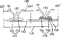
Specifically describe the LCD of another embodiment according to the present invention with reference to accompanying drawing 13 to 15.
Figure 13 is the arrangenent diagram of the LCD of another embodiment of the present invention; Figure 14 is the sectional view that LCD XIV-XIV ' along the line shown in Figure 13 dissects, and Figure 15 is XV-XV ' along the line and the XV '-XV of LCD shown in Figure 13 " sectional view that dissects.
With reference to Figure 13 to 15, the LCD of present embodiment also comprises tft array plate 100, common electrode plate 200 and places therebetween LC layer 300.
The plate 100 of present embodiment and 200 hierarchy be identical with shown in Figure 11 to 12 almost.
For tft array plate 100, in substrate 110, form many gate lines 121 comprise a plurality of gate electrodes 123, and gate insulator 140, comprise a plurality of semiconductor tapes 151 of a plurality of projections 154 and comprise a plurality of Ohmic contact bands 161 of a plurality of projections 163 and a plurality of Ohmic contact island 165 formed thereon successively.Many the data lines 171 and a plurality of drain electrode 175 that comprise multiple source electrode 173 are formed on Ohmic contact 161 and 165, and passivation layer 180 is formed thereon.A plurality of contact holes 181,182 and 183 are set on passivation layer 180 and gate insulator 140, and a plurality of pixel electrodes 190 are formed on the passivation layer 180 with a plurality of slave parts 95 and 97 that contact.
For common electrode plate 200, on dielectric base 210, form light blocking parts 220, a plurality of light filter 230, superstratum 250, have the common electrode 270 of a plurality of openings 279.
Different with the LCD shown in Figure 11 and 12 is, the tft array plate of present embodiment is provided with many storage electrode lines 131, and it separates with gate line 121, and with gate line 121 on identical layer, and do not have the projection of gate line 121.Storage electrode line 131 provides predetermined voltage, for example common voltage.In addition, under the situation that the storage capacitor conductor 177 shown in Figure 11 and 12 is not set, drain electrode 175 is extended covering storage electrode line 131 and is formed reservior capacitor.If the storage capacitors that is produced by the overlapping of gate line 121 and pixel electrode 191 is enough big, can save storage electrode line 131.
And semiconductor tape 151 has and data line 171 and drain electrode 175 and following Ohmic contact 161 and 165 flat shape much at one.But the projection 154 of semiconductor tape 151 comprises some expose portions, and these parts are not covered by data line 171 and drain electrode 175, for example the part between source electrode 173 and the drain electrode 175.
The a lot of characteristics of LCD shown in described Figure 11 and 12 are applicable to the LCD shown in Figure 13 to 15.
Specifically describe the LCD of the another embodiment of the present invention with reference to accompanying drawing 16 and 17.
Figure 16 is the arrangenent diagram of the LCD of the another embodiment of the present invention; Figure 17 is the sectional view of the tft array plate that dissects of LCD XVII-XVII ' along the line shown in Figure 16.
With reference to Figure 16 and 17, the LCD of present embodiment also comprises tft array plate 100, common electrode plate (not shown) and places therebetween LC layer (not shown).
The hierarchy of the plate of present embodiment is identical with shown in Figure 11 to 12 almost.
For tft array plate 100, in substrate 110, form many gate lines 121 comprise a plurality of gate electrodes 123 and a plurality of projection 127, and gate insulator 140, comprise a plurality of semiconductor tapes 151 of a plurality of projections 154 and comprise a plurality of Ohmic contact bands 161 of a plurality of projections 163 and a plurality of Ohmic contact island 165 formed thereon successively.Many data lines 171, a plurality of drain electrode 175 and a plurality of storage capacitor conductors 177 that comprises multiple source electrode 173 be formed on Ohmic contact 161 and 165 and gate insulator 140 on, passivation layer 180 is formed thereon.A plurality of contact holes 181,182,183 and 187 are set on passivation layer 180 and gate insulator 140, and a plurality of pixel electrodes 190 are formed on the passivation layer 180 with a plurality of slave parts 95 and 97 that contact.
For the common electrode plate, the common electrode (not shown) that on dielectric base 210, forms light blocking parts (not shown) and have a plurality of openings 279.
Different with the LCD shown in Figure 11 and 12 is that the tft array plate of present embodiment is provided with a plurality of red, green and blue look light filter band R, G and B for 180 times at passivation layer, and does not establish light filter on the common electrode plate.Each light filter band R, G and B are substantially disposed between two adjacent data lines 171, and extend longitudinally.Light filter band R, G and B have a plurality of open C 1 and C2, and these openings expose drain electrode 175 and storage capacitor conductor 177, and respectively around contact hole 181 and 187.Yet contact hole 181 and 187 can all expose open C 1 and C2, can also expose the upper surface of light filter R, G and B, make pixel electrode 190 thus and drain 175 and the contact profile of 177 of storage capacitor conductors level and smooth.Light filter band R, G and B are not arranged on expansion end 125 with gate line 121 and data line 179 and 179 neighboring area.Although the limit of adjacent light filter band R, G and B shown in the figure accurately cooperates each other, light filter band R, G and B can overlap each other on data line 171 and stop that with what strengthen light perhaps it can separate each other.
And, on the common electrode plate, there is not superstratum, this is selectable certainly.
The a lot of characteristics of LCD shown in described Figure 11 and 12 are applicable to the LCD shown in Figure 16 and 17.
Specifically describe according to the present invention the LCD of an embodiment again with reference to accompanying drawing 18 to 22.
Figure 18 is the present invention's arrangenent diagram of the tft array plate of the LCD of an embodiment again; Figure 19 is the present invention's arrangenent diagram of the common electrode of the LCD of an embodiment again; Figure 20 is the arrangenent diagram that comprises the LCD of tft array plate shown in Figure 180 and common electrode plate shown in Figure 19; Figure 21 is the sectional view that LCD XXI-XXI ' along the line shown in Figure 20 dissects; Figure 22 is LCD XXII-XXII ' along the line and XXII '-XXII shown in Figure 20 " sectional view that dissects.
With reference to Figure 18 to 22, the LCD of present embodiment also comprises tft array plate 100, common electrode plate 200 and places therebetween LC layer 300.
The plate 100 of present embodiment and 200 hierarchy be identical with shown in Fig. 1 to 5 almost.
For tft array plate 100, in substrate 110, form many gate lines 121 and the many storage electrode lines 131 comprise a plurality of gate electrodes 123, make gate insulator 140, comprise a plurality of semiconductor tapes 151 of a plurality of projections 154 and comprise a plurality of Ohmic contact bands 161 of a plurality of projections 163 and a plurality of Ohmic contact island 165 formed thereon successively.Many the data lines 171 and a plurality of drain electrode 175 that comprise multiple source electrode 173 are formed on Ohmic contact 161 and 165, make passivation layer 180 formed thereon.A plurality of contact holes 181,182 and 183 are set on passivation layer 180 and gate insulator 140, and a plurality of pixel electrodes 190 are formed on the passivation layer 180 with a plurality of slave parts 95 and 97 that contact.Alignment 11 is formed thereon.
For common electrode plate 200, on dielectric base 210, form light blocking parts 220, a plurality of light filter 230, superstratum 250, common electrode 270 and alignment 21 with a plurality of otch 271.
Different with the LCD shown in Fig. 1 to 5 is, storage electrode line 131 is arranged near the center of pixel electrode 190, and it comprises a plurality of branches that are parallel to data line 171 and tilt to extend up and down, to form storage electrode 133.In addition, drain electrode 175 also prolongs along storage electrode 133, and storage electrode 133 and drain electrode 175 are overlapping with the otch 271 of common electrode 270.But pixel electrode 190 does not have independent rectangle, rhombus or parallelogram opening.
Because storage electrode 133 is overlapping with drain electrode 175 by very long distance, so obtained enough big storage capacitors.And because storage electrode 133 and drain electrode 175 are overlapping with otch 271, so it prolongs the reduction that does not cause the aperture ratio.So, compare with the structure shown in Fig. 1 to 5, by save opening in common electrode 270, the aperture ratio can obtain sizable raising.
In addition, because storage electrode 133 and drain electrode are arranged on the border in territory, so the degree of freedom of pixel design and storage capacitors is very high.
The a lot of characteristics of LCD shown in described Fig. 1 to 5 are applicable to the LCD shown in Figure 18 to 22.
Specifically describe the LCD of another embodiment of the present invention with reference to Figure 23 to 25.
Figure 23 is the arrangenent diagram of tft array plate of the LCD of another embodiment of the present invention; Figure 24 is the sectional view that comprises that the LCD XXIV-XXIV ' along the line of tft array plate shown in Figure 23 dissects; Figure 25 is LCD XXV-XXV ' along the line and the XXV '-XXV that comprises tft array plate shown in Figure 23 " sectional view that dissects.
With reference to Figure 23 to 25, the LCD of present embodiment also comprises tft array plate 100, common electrode plate 200 and places therebetween LC layer 300.
The plate 100 of present embodiment is almost identical with the structure shown in Figure 18 to 22 with 200 hierarchy.Particularly, common electrode plate 200 can have and essentially identical design shown in Figure 19.
For tft array plate 100, in substrate 110, form many gate lines 121 comprise a plurality of gate electrodes 123 and many storage electrode lines 131 that comprise a plurality of storage electrodes 133, make gate insulator 140, comprise a plurality of semiconductor tapes 151 of a plurality of projections 154 and comprise a plurality of Ohmic contact bands 161 of a plurality of projections 163 and a plurality of Ohmic contact island 165 formed thereon successively.Many the data lines 171 and a plurality of drain electrode 175 that comprise multiple source electrode 173 are formed on Ohmic contact 161 and 165, and passivation layer 180 is formed thereon.A plurality of contact holes 181,182 and 183 are set on passivation layer 180 and gate insulator 140, and a plurality of pixel electrodes 190 are formed on the passivation layer 180 with a plurality of slave parts 95 and 97 that contact.Alignment 11 is formed thereon.
For common electrode plate 200, on dielectric base 210, form light blocking parts 220, a plurality of light filter 230, superstratum 250, common electrode 270 and alignment 21 with a plurality of otch 271.
Different with the LCD shown in Figure 18 to 22 is that semiconductor tape 151 has and data line 171, drain electrode 175 and following Ohmic contact 161 and 165 flat shape much at one.But the projection 154 of semiconductor tape 151 comprises that some are not by the expose portion of data line 171 and drain electrode 175 coverings, for example part between source electrode 173 and drain electrode 175.
The a lot of characteristics of LCD shown in described Figure 18 to 22 are applicable to the LCD shown in Figure 23 to 25.
Specifically describe the LCD of another embodiment according to the present invention with reference to accompanying drawing 26 and 27.
Figure 26 is the arrangenent diagram of the LCD of the another embodiment of the present invention; Figure 27 is the sectional view that LCD XXVII-XXVII ' along the line shown in Figure 26 dissects.
With reference to Figure 26 and 27, the LCD of present embodiment also comprises tft array plate 100, common electrode plate 200 and places therebetween LC layer 300.
Almost identical according to the plate 100 of present embodiment with the structure shown in Figure 18 to 22 with 200 hierarchy.
For tft array plate 100, in substrate 110, form many gate lines 121 comprise a plurality of gate electrodes 123 and many storage electrode lines 131 that comprise a plurality of storage electrodes 133, make gate insulator 140, comprise a plurality of semiconductor tapes 151 of a plurality of projections 154 and comprise a plurality of Ohmic contact bands 161 of a plurality of projections 163 and a plurality of Ohmic contact island 165 formed thereon successively.Many the data lines 171 and a plurality of drain electrode 175 that comprise multiple source electrode 173 are formed on Ohmic contact 161 and 165, and passivation layer 180 is formed thereon.A plurality of contact holes 181,182 and 183 are set on passivation layer 180 and gate insulator 140, and a plurality of pixel electrodes 190 are formed on the passivation layer 180 with a plurality of slave parts 95 and 97 that contact.
For common electrode plate 200, on dielectric base 210, form light blocking parts 220, superstratum 250 and have the common electrode 270 of a plurality of otch 271.
Different with the LCD shown in Figure 18 to 22 is that each pixel electrode 190 has otch 191.Each otch 191 comprises the sloping portion that pair of parallel is extended in data line 171, and pixel electrode 190 is divided into a left side and the right half that forms a pair of sub-pixel area Pa and Pb.In addition, common electrode 270 has and is parallel to otch 191 and pixel electrode 190 divided into a left side and right half many to otch 271a and 271b.
In addition, a plurality of red, green and blue look light filter band R, G and B be formed on passivation layer 180 below, and on the common electrode plate, do not establish light filter.Each light filter band R, G and B are arranged between two adjacent data lines 171 basically and extend longitudinally, thereby along data line 171 cycle bending.Contact hole 181 also passes light filter band R, G and B, thereby exposes drain electrode 175.Light filter band R, G and B are not arranged on expansion end 125 with gate line 121 and data line 171 and 179 neighboring area.Although the edge of adjacent light filter band R, G and B shown in the figure accurately cooperates each other, light filter band R, G and B can overlap each other on data line 171, stop that with what improve light perhaps they can separate each other.
Although the subregion of a pair of formation pixel electrode 190 shown in the figure is placed between the adjacent data line 171, these subregions can be by data line 171 separately.
The a lot of characteristics of LCD shown in described Figure 18 to 22 are applicable to the LCD shown in Figure 26 and 27.
Although the pixel electrode shown in Figure 18 to 27 190, data line 171 etc. are crooked, it can be straight or right angle.In addition, the type of the shape of otch 191,271,271a and 271b and layout and LC layer 300 and alignment so can change.
As mentioned above, embodiments of the present invention are provided with opening at common electrode, and this has prevented the increase of LC electric capacity and storage capacitors is increased, has improved the charge rate and the aperture ratio of LC capacitor thus.In addition, these embodiments make storage electrode or drain electrode face the otch of common electrode, and they are crooked as the pixel electrode, have improved the degree of freedom of pixel design thus, and have improved storage capacitors and aperture ratio.
Though specifically described the present invention with reference to preferred implementation, it will be understood by those skilled in the art that under the prerequisite that does not exceed the design of the present invention that proposes as appended claims and scope, can carry out various remodeling and replacement to it.
Claims (36)
1. LCD comprises:
One film transistor array plate, it comprises:
First grid polar curve,
With the crossing data line of described gate line,
The first film transistor, it comprises the gate electrode that is connected with described gate line, the source electrode that is connected with described data line and drain electrode,
First pixel electrode that is connected with described drain electrode,
With one of at least overlapping in described pixel electrode and the described drain electrode and accompany the electrode for capacitors of insulator; And
One in the face of the common electrode plate of described film transistor array plate, and it comprises in the face of described pixel electrode and has in the face of one of at least the common electrode of opening in described drain electrode and the described electrode for capacitors.
2. LCD according to claim 1, wherein, described data line comprises sweep and the cross section that is connected with described sweep and intersects with described gate line.
3. LCD according to claim 2, wherein, the sweep of described data line comprises a pair of straight line portion that is connected to each other and becomes about miter angle with described gate line.
4. LCD according to claim 2, wherein, described pixel electrode is along the sweep bending of described data line.
5. LCD according to claim 1, wherein, described pixel electrode is overlapping with described data line at least in part.
6. LCD according to claim 1 wherein, also comprises:
With described first grid polar curve and described data line separates and contiguous described first pixel electrode is provided with second grid line;
Second thin film transistor (TFT) that is connected with described second grid line; And
Second pixel electrode that is connected with described second thin film transistor (TFT).
7. LCD according to claim 6, wherein, described electrode for capacitors is connected with described second grid line.
8. LCD according to claim 7 wherein, also comprises and described pixel electrode electrically connects and be arranged on capacitor conductor between described electrode for capacitors and the described pixel electrode.
9. LCD according to claim 6, wherein, described electrode for capacitors and described second grid line disconnect.
10. LCD according to claim 1 wherein, also comprises the light filter on any one that is arranged on described film transistor array plate and described common electrode plate.
11. LCD according to claim 1 wherein, also comprises the liquid crystal layer that places between described film transistor array plate and the described common electrode plate.
12. LCD according to claim 11, wherein, described liquid crystal layer has negative anisotropy and perpendicular is aimed at.
13. LCD according to claim 12 wherein, also comprises the inclination control assembly of the vergence direction of molecule in the described liquid crystal layer of control.
14. LCD according to claim 13, wherein, described inclination control assembly comprises the otch that is in described pixel electrode or the described common electrode.
15. LCD according to claim 13, wherein, described inclination control assembly is included in the projection on described pixel electrode or the described common electrode.
16. LCD according to claim 1 wherein, also comprises and described gate electrode is oppositely arranged and comprises the semiconductor layer of the first between described source electrode and described drain electrode.
17. LCD according to claim 16, wherein, described semiconductor layer also comprises the second portion that is arranged under the described data line.
18. LCD according to claim 17, wherein, except that described first, described semiconductor layer has and described data line, described source electrode and the essentially identical planar graph of described drain electrode.
19. a film transistor array plate comprises:
Substrate;
Be formed in the described substrate and comprise the gate line of gate electrode;
Be formed in the described substrate and comprise sweep and the data line of the cross section that intersects with described gate line;
The thin film transistor (TFT) that comprises the gate electrode that is connected with described gate line, the source electrode that is connected with described data line and drain electrode;
The pixel electrode that is connected with described drain electrode; And
With one of at least overlapping in described pixel electrode and the described drain electrode and accompany the storage electrode of insulator,
Wherein, comprise one of at least the part of extending in described drain electrode and the described storage electrode along the described sweep that is parallel to described data line.
20. film transistor array plate according to claim 19, wherein, the described sweep of described data line comprises a pair of part that becomes the clockwise angle and the about 45 counterclockwise angles of spending of about 45 degree with respect to described gate line respectively.
21. film transistor array plate according to claim 19, wherein, described drain electrode and described storage electrode overlap each other.
22. film transistor array plate according to claim 19, wherein, described source electrode is connected with the cross section of described data line.
23. film transistor array plate according to claim 19, wherein, described pixel electrode is along the described sweep bending of described data line.
24. film transistor array plate according to claim 19, wherein, described pixel electrode is overlapping with described data line at least in part.
25. film transistor array plate according to claim 19 wherein, is provided with a pair of subregion of otch between described pixel electrode comprises.
26. film transistor array plate according to claim 19 wherein, also comprises and described gate electrode is oppositely arranged and comprises the semiconductor layer of the first between described source electrode and described drain electrode.
27. film transistor array plate according to claim 26, wherein, described semiconductor layer also comprises the second portion that is arranged under the described data line.
28. film transistor array plate according to claim 27, wherein, except that described first, described semiconductor layer has and described data line, described source electrode and the essentially identical planar graph of described drain electrode.
29. a LCD comprises:
One film transistor array plate, it comprises:
Substrate,
Be formed in the described substrate and comprise the gate line of gate electrode,
Be formed in the described substrate and comprise sweep and the data line of the cross section that intersects with described gate line,
The thin film transistor (TFT) that comprises the gate electrode that is connected with described gate line, the source electrode that is connected with described data line and drain electrode,
The pixel electrode that is connected with described drain electrode,
With one of at least overlapping in described pixel electrode and the described drain electrode and accompany the storage electrode of insulator; And
The one common electrode plate in the face of described film transistor array plate, it comprises the common electrode in the face of described pixel electrode.
30. LCD according to claim 29 wherein, also comprises the light filter on any one that is arranged on described film transistor array plate and described common electrode plate.
31. LCD according to claim 29 wherein, also comprises placing between described film transistor array plate and the described common electrode plate and having negative anisotropy and liquid crystal layer that perpendicular is aimed at.
32. LCD according to claim 29 wherein, also comprises the inclination control assembly of the vergence direction of molecule in the described liquid crystal layer of control.
33. LCD according to claim 32, wherein, described inclination control assembly is included in the otch in described pixel electrode or the described common electrode.
34. LCD according to claim 32, wherein, described inclination control assembly is included in the projection on described pixel electrode or the described common electrode.
35. LCD according to claim 32, wherein, described inclination control assembly and described data line are crooked abreast.
36. LCD according to claim 35, wherein, described inclination control assembly in the face of in described drain electrode and the described storage electrode one of at least.
Applications Claiming Priority (4)
| Application Number | Priority Date | Filing Date | Title |
|---|---|---|---|
| KR1020030031628A KR101018756B1 (en) | 2003-05-19 | 2003-05-19 | Liquid crystal display |
| KR0031628/2003 | 2003-05-19 | ||
| KR0031835/2003 | 2003-05-20 | ||
| KR1020030031835A KR100992121B1 (en) | 2003-05-20 | 2003-05-20 | Thin film transistor array panel and liquid crystal display including the panel |
Related Child Applications (1)
| Application Number | Title | Priority Date | Filing Date |
|---|---|---|---|
| CNA2008101084865A Division CN101290939A (en) | 2003-05-19 | 2004-05-19 | Liquid crystal display and it thin film transistor array substrate |
Publications (1)
| Publication Number | Publication Date |
|---|---|
| CN1591152A true CN1591152A (en) | 2005-03-09 |
Family
ID=33455685
Family Applications (1)
| Application Number | Title | Priority Date | Filing Date |
|---|---|---|---|
| CNA2004100794360A Pending CN1591152A (en) | 2003-05-19 | 2004-05-19 | Liquid crystal display and thin film transistor array panel therefor |
Country Status (4)
| Country | Link |
|---|---|
| US (1) | US20040233343A1 (en) |
| JP (1) | JP2004348130A (en) |
| CN (1) | CN1591152A (en) |
| TW (1) | TW200510843A (en) |
Cited By (3)
| Publication number | Priority date | Publication date | Assignee | Title |
|---|---|---|---|---|
| CN1916702B (en) * | 2005-04-29 | 2010-05-26 | 统宝光电股份有限公司 | Liquid crystal displays |
| US7880857B2 (en) | 2005-12-26 | 2011-02-01 | Sharp Kabushiki Kaisha | Active matrix substrate, display device, television receiver, and method for repairing defects of active matrix substrate |
| CN103713429A (en) * | 2013-06-04 | 2014-04-09 | 友达光电股份有限公司 | Pixel structure |
Families Citing this family (24)
| Publication number | Priority date | Publication date | Assignee | Title |
|---|---|---|---|---|
| US7256849B2 (en) * | 2003-06-11 | 2007-08-14 | Samsung Electronics Co., Ltd. | Liquid crystal display |
| KR101133757B1 (en) * | 2004-11-25 | 2012-04-09 | 삼성전자주식회사 | Liquid crystal display |
| KR101197044B1 (en) * | 2004-12-02 | 2012-11-06 | 삼성디스플레이 주식회사 | Liquid crystal display |
| KR101112551B1 (en) * | 2005-02-07 | 2012-02-15 | 삼성전자주식회사 | Liquid crystal display and driving method thereof |
| JP4716782B2 (en) * | 2005-05-24 | 2011-07-06 | シャープ株式会社 | Liquid crystal display device and manufacturing method thereof |
| KR101153942B1 (en) * | 2005-07-20 | 2012-06-08 | 삼성전자주식회사 | Liquid crystal display |
| KR20070014715A (en) * | 2005-07-29 | 2007-02-01 | 삼성전자주식회사 | Array substrate having enhanced aperture ratio, and method of manufacturing the same |
| JP5144055B2 (en) * | 2005-11-15 | 2013-02-13 | 三星電子株式会社 | Display substrate and display device having the same |
| KR101383714B1 (en) * | 2005-12-02 | 2014-04-09 | 삼성디스플레이 주식회사 | Liquid crystal display |
| KR101231867B1 (en) * | 2006-02-23 | 2013-02-08 | 삼성디스플레이 주식회사 | Liquid Crystal Display Apparatus |
| JP4846402B2 (en) * | 2006-03-20 | 2011-12-28 | スタンレー電気株式会社 | Liquid crystal display element |
| KR20080000458A (en) * | 2006-06-27 | 2008-01-02 | 삼성전자주식회사 | Liquid crystal display device |
| JP5376774B2 (en) * | 2006-07-21 | 2013-12-25 | 三星ディスプレイ株式會社 | Liquid crystal display |
| KR101358827B1 (en) * | 2006-07-24 | 2014-02-06 | 삼성디스플레이 주식회사 | Liquid crystal display |
| KR101393637B1 (en) * | 2006-11-23 | 2014-05-12 | 삼성디스플레이 주식회사 | Display panel |
| KR101300819B1 (en) * | 2006-12-05 | 2013-08-26 | 삼성디스플레이 주식회사 | Liquid crystal display and method of manufacturing the same |
| KR101394434B1 (en) * | 2007-06-29 | 2014-05-15 | 삼성디스플레이 주식회사 | Display apparatus and driving method thereof |
| JP4568312B2 (en) * | 2007-08-30 | 2010-10-27 | 株式会社 日立ディスプレイズ | Liquid crystal display |
| TWI339304B (en) * | 2007-10-16 | 2011-03-21 | Au Optronics Corp | Pixel structure, driving method thereof and pixel array structure |
| JP5175127B2 (en) * | 2008-03-28 | 2013-04-03 | 株式会社ジャパンディスプレイウェスト | Liquid crystal display |
| KR101499227B1 (en) * | 2008-08-20 | 2015-03-06 | 삼성디스플레이 주식회사 | Thin film transistor panel and method of manufacturing for the same |
| WO2010102027A1 (en) | 2009-03-04 | 2010-09-10 | Xerox Corporation | Composite structured organic films |
| KR101250318B1 (en) * | 2009-05-22 | 2013-04-03 | 엘지디스플레이 주식회사 | Array substrate for fringe field switching mode liquid crystal display device |
| CN114415431A (en) * | 2020-10-28 | 2022-04-29 | 瀚宇彩晶股份有限公司 | Display panel and manufacturing method thereof |
Family Cites Families (16)
| Publication number | Priority date | Publication date | Assignee | Title |
|---|---|---|---|---|
| KR970004883B1 (en) * | 1992-04-03 | 1997-04-08 | 삼성전자 주식회사 | Liquid crystal display panel |
| TW373114B (en) * | 1996-08-05 | 1999-11-01 | Sharp Kk | Liquid crystal display device |
| JP3966614B2 (en) * | 1997-05-29 | 2007-08-29 | 三星電子株式会社 | Wide viewing angle LCD |
| JP2000002889A (en) * | 1998-06-16 | 2000-01-07 | Mitsubishi Electric Corp | Liquid crystal display device |
| JP2000155318A (en) * | 1998-09-18 | 2000-06-06 | Fujitsu Ltd | Liquid crystal display device |
| KR100312753B1 (en) * | 1998-10-13 | 2002-04-06 | 윤종용 | Wide viewing angle liquid crystal display device |
| US6593982B2 (en) * | 1999-11-01 | 2003-07-15 | Samsung Electronics Co., Ltd. | Liquid crystal display with color filter having depressed portion for wide viewing angle |
| US7119870B1 (en) * | 1998-11-27 | 2006-10-10 | Sanyo Electric Co., Ltd. | Liquid crystal display device having particular drain lines and orientation control window |
| JP3378820B2 (en) * | 1999-01-20 | 2003-02-17 | 三洋電機株式会社 | Vertical alignment type liquid crystal display |
| JP3969887B2 (en) * | 1999-03-19 | 2007-09-05 | シャープ株式会社 | Liquid crystal display device and manufacturing method thereof |
| US6504592B1 (en) * | 1999-06-16 | 2003-01-07 | Nec Corporation | Liquid crystal display and method of manufacturing the same and method of driving the same |
| JP2001183648A (en) * | 1999-12-24 | 2001-07-06 | Nec Corp | Color liquid crystal display device and method of producing the same |
| TW514762B (en) * | 2000-03-06 | 2002-12-21 | Hitachi Ltd | Liquid crystal display element having controlled storage capacitance |
| KR20020042898A (en) * | 2000-12-01 | 2002-06-08 | 구본준, 론 위라하디락사 | Liquid crystal display device and method of manufacturing thereof |
| KR100748442B1 (en) * | 2001-02-26 | 2007-08-10 | 엘지.필립스 엘시디 주식회사 | a array panel of in plane switching mode liquid crystal display and manufacturing method thereof |
| JP4049589B2 (en) * | 2002-01-18 | 2008-02-20 | シャープ株式会社 | Substrate for liquid crystal display device, liquid crystal display device including the same, and manufacturing method thereof |
-
2004
- 2004-05-18 US US10/848,298 patent/US20040233343A1/en not_active Abandoned
- 2004-05-19 JP JP2004148528A patent/JP2004348130A/en not_active Abandoned
- 2004-05-19 TW TW093114103A patent/TW200510843A/en unknown
- 2004-05-19 CN CNA2004100794360A patent/CN1591152A/en active Pending
Cited By (5)
| Publication number | Priority date | Publication date | Assignee | Title |
|---|---|---|---|---|
| CN1916702B (en) * | 2005-04-29 | 2010-05-26 | 统宝光电股份有限公司 | Liquid crystal displays |
| US7880857B2 (en) | 2005-12-26 | 2011-02-01 | Sharp Kabushiki Kaisha | Active matrix substrate, display device, television receiver, and method for repairing defects of active matrix substrate |
| US8045076B2 (en) | 2005-12-26 | 2011-10-25 | Sharp Kabushiki Kaisha | Active matrix substrate, display device, television receiver, and method for repairing defects of active matrix substrate |
| CN103713429A (en) * | 2013-06-04 | 2014-04-09 | 友达光电股份有限公司 | Pixel structure |
| CN103713429B (en) * | 2013-06-04 | 2016-08-10 | 友达光电股份有限公司 | Pixel structure |
Also Published As
| Publication number | Publication date |
|---|---|
| TW200510843A (en) | 2005-03-16 |
| US20040233343A1 (en) | 2004-11-25 |
| JP2004348130A (en) | 2004-12-09 |
Similar Documents
| Publication | Publication Date | Title |
|---|---|---|
| CN1591152A (en) | Liquid crystal display and thin film transistor array panel therefor | |
| CN1605921A (en) | Liquid crystal display and thin film transistor substrate therefor | |
| CN1540426A (en) | LCD device its used thin film transistor array plate and mfg. method thereof | |
| CN1270389C (en) | Film transistor and its mfg. method | |
| CN100335959C (en) | Thin film transistor array substrate, method of fabricating the same, liquid crystal display panel having the same and fabricating method thereof | |
| CN1178098C (en) | Liquid crystal display | |
| CN1495478A (en) | Contact structure and mfg. method, thin film transistor array panel and mfg. method | |
| CN100340914C (en) | Display device and photoelectric conversion device | |
| CN1639624A (en) | Liquid crystal display and thin film transistor array panel therefor | |
| CN1221845C (en) | Active-matrix addressing LCD device using laterial electric field | |
| CN1761049A (en) | Thin-film transistor display panel and manufacture method thereof | |
| CN1794067A (en) | Liquid crystal display and panel therefor | |
| CN1619403A (en) | Thin film transistor array panel and liquid crystal display including the same | |
| CN1542531A (en) | Liquid crystal display and thin film transistor array panel therefor | |
| CN1808252A (en) | Thin film transistor array panel and liquid crystal display including the panel | |
| CN1808709A (en) | Thin film transistor array panel and manufacturing method thereof | |
| CN1601361A (en) | Liquid crystal display | |
| CN1488083A (en) | Thin film transistor array substrate of liquid crystal display device and producing method thereof | |
| CN1542709A (en) | Electro-optical device and electronic apparatus | |
| CN1758126A (en) | LCD and thin-film transistor display panel thereof | |
| CN1821872A (en) | Etchant composition and manufacturing method for thin film transistor array panel | |
| CN101055361A (en) | Lateral electric field type liquid-crystal display device | |
| CN1771595A (en) | Contact portion and manufacturing method thereof, thin film transistor array panel and manufacturing method thereof | |
| CN1573488A (en) | Liquid crystal display and thin film transistor array panel therefor | |
| CN1295343A (en) | Electrooptical device, its manufacture and electronic machine |
Legal Events
| Date | Code | Title | Description |
|---|---|---|---|
| C06 | Publication | ||
| PB01 | Publication | ||
| C10 | Entry into substantive examination | ||
| SE01 | Entry into force of request for substantive examination | ||
| C02 | Deemed withdrawal of patent application after publication (patent law 2001) | ||
| WD01 | Invention patent application deemed withdrawn after publication |