CN102844151A - Hydrostatic pad pressure modulation in a simultaneous double side wafer grinder - Google Patents
Hydrostatic pad pressure modulation in a simultaneous double side wafer grinder Download PDFInfo
- Publication number
- CN102844151A CN102844151A CN201180016139XA CN201180016139A CN102844151A CN 102844151 A CN102844151 A CN 102844151A CN 201180016139X A CN201180016139X A CN 201180016139XA CN 201180016139 A CN201180016139 A CN 201180016139A CN 102844151 A CN102844151 A CN 102844151A
- Authority
- CN
- China
- Prior art keywords
- wafer
- abrasive wheel
- pad
- hydrostatic
- grinder
- Prior art date
- Legal status (The legal status is an assumption and is not a legal conclusion. Google has not performed a legal analysis and makes no representation as to the accuracy of the status listed.)
- Pending
Links
Images


Classifications
-
- B—PERFORMING OPERATIONS; TRANSPORTING
- B24—GRINDING; POLISHING
- B24B—MACHINES, DEVICES, OR PROCESSES FOR GRINDING OR POLISHING; DRESSING OR CONDITIONING OF ABRADING SURFACES; FEEDING OF GRINDING, POLISHING, OR LAPPING AGENTS
- B24B37/00—Lapping machines or devices; Accessories
- B24B37/04—Lapping machines or devices; Accessories designed for working plane surfaces
- B24B37/042—Lapping machines or devices; Accessories designed for working plane surfaces operating processes therefor
-
- B—PERFORMING OPERATIONS; TRANSPORTING
- B24—GRINDING; POLISHING
- B24B—MACHINES, DEVICES, OR PROCESSES FOR GRINDING OR POLISHING; DRESSING OR CONDITIONING OF ABRADING SURFACES; FEEDING OF GRINDING, POLISHING, OR LAPPING AGENTS
- B24B1/00—Processes of grinding or polishing; Use of auxiliary equipment in connection with such processes
-
- B—PERFORMING OPERATIONS; TRANSPORTING
- B24—GRINDING; POLISHING
- B24B—MACHINES, DEVICES, OR PROCESSES FOR GRINDING OR POLISHING; DRESSING OR CONDITIONING OF ABRADING SURFACES; FEEDING OF GRINDING, POLISHING, OR LAPPING AGENTS
- B24B37/00—Lapping machines or devices; Accessories
- B24B37/04—Lapping machines or devices; Accessories designed for working plane surfaces
- B24B37/07—Lapping machines or devices; Accessories designed for working plane surfaces characterised by the movement of the work or lapping tool
- B24B37/08—Lapping machines or devices; Accessories designed for working plane surfaces characterised by the movement of the work or lapping tool for double side lapping
-
- B—PERFORMING OPERATIONS; TRANSPORTING
- B24—GRINDING; POLISHING
- B24B—MACHINES, DEVICES, OR PROCESSES FOR GRINDING OR POLISHING; DRESSING OR CONDITIONING OF ABRADING SURFACES; FEEDING OF GRINDING, POLISHING, OR LAPPING AGENTS
- B24B37/00—Lapping machines or devices; Accessories
- B24B37/27—Work carriers
- B24B37/28—Work carriers for double side lapping of plane surfaces
-
- B—PERFORMING OPERATIONS; TRANSPORTING
- B24—GRINDING; POLISHING
- B24B—MACHINES, DEVICES, OR PROCESSES FOR GRINDING OR POLISHING; DRESSING OR CONDITIONING OF ABRADING SURFACES; FEEDING OF GRINDING, POLISHING, OR LAPPING AGENTS
- B24B49/00—Measuring or gauging equipment for controlling the feed movement of the grinding tool or work; Arrangements of indicating or measuring equipment, e.g. for indicating the start of the grinding operation
-
- B—PERFORMING OPERATIONS; TRANSPORTING
- B24—GRINDING; POLISHING
- B24B—MACHINES, DEVICES, OR PROCESSES FOR GRINDING OR POLISHING; DRESSING OR CONDITIONING OF ABRADING SURFACES; FEEDING OF GRINDING, POLISHING, OR LAPPING AGENTS
- B24B7/00—Machines or devices designed for grinding plane surfaces on work, including polishing plane glass surfaces; Accessories therefor
- B24B7/10—Single-purpose machines or devices
- B24B7/16—Single-purpose machines or devices for grinding end-faces, e.g. of gauges, rollers, nuts, piston rings
- B24B7/17—Single-purpose machines or devices for grinding end-faces, e.g. of gauges, rollers, nuts, piston rings for simultaneously grinding opposite and parallel end faces, e.g. double disc grinders
-
- B—PERFORMING OPERATIONS; TRANSPORTING
- B24—GRINDING; POLISHING
- B24B—MACHINES, DEVICES, OR PROCESSES FOR GRINDING OR POLISHING; DRESSING OR CONDITIONING OF ABRADING SURFACES; FEEDING OF GRINDING, POLISHING, OR LAPPING AGENTS
- B24B9/00—Machines or devices designed for grinding edges or bevels on work or for removing burrs; Accessories therefor
- B24B9/02—Machines or devices designed for grinding edges or bevels on work or for removing burrs; Accessories therefor characterised by a special design with respect to properties of materials specific to articles to be ground
- B24B9/06—Machines or devices designed for grinding edges or bevels on work or for removing burrs; Accessories therefor characterised by a special design with respect to properties of materials specific to articles to be ground of non-metallic inorganic material, e.g. stone, ceramics, porcelain
- B24B9/08—Machines or devices designed for grinding edges or bevels on work or for removing burrs; Accessories therefor characterised by a special design with respect to properties of materials specific to articles to be ground of non-metallic inorganic material, e.g. stone, ceramics, porcelain of glass
- B24B9/14—Machines or devices designed for grinding edges or bevels on work or for removing burrs; Accessories therefor characterised by a special design with respect to properties of materials specific to articles to be ground of non-metallic inorganic material, e.g. stone, ceramics, porcelain of glass of optical work, e.g. lenses, prisms
- B24B9/148—Machines or devices designed for grinding edges or bevels on work or for removing burrs; Accessories therefor characterised by a special design with respect to properties of materials specific to articles to be ground of non-metallic inorganic material, e.g. stone, ceramics, porcelain of glass of optical work, e.g. lenses, prisms electrically, e.g. numerically, controlled
-
- H—ELECTRICITY
- H01—ELECTRIC ELEMENTS
- H01L—SEMICONDUCTOR DEVICES NOT COVERED BY CLASS H10
- H01L21/00—Processes or apparatus adapted for the manufacture or treatment of semiconductor or solid state devices or of parts thereof
- H01L21/02—Manufacture or treatment of semiconductor devices or of parts thereof
- H01L21/04—Manufacture or treatment of semiconductor devices or of parts thereof the devices having at least one potential-jump barrier or surface barrier, e.g. PN junction, depletion layer or carrier concentration layer
- H01L21/18—Manufacture or treatment of semiconductor devices or of parts thereof the devices having at least one potential-jump barrier or surface barrier, e.g. PN junction, depletion layer or carrier concentration layer the devices having semiconductor bodies comprising elements of Group IV of the Periodic System or AIIIBV compounds with or without impurities, e.g. doping materials
- H01L21/30—Treatment of semiconductor bodies using processes or apparatus not provided for in groups H01L21/20 - H01L21/26
- H01L21/302—Treatment of semiconductor bodies using processes or apparatus not provided for in groups H01L21/20 - H01L21/26 to change their surface-physical characteristics or shape, e.g. etching, polishing, cutting
- H01L21/304—Mechanical treatment, e.g. grinding, polishing, cutting
-
- H—ELECTRICITY
- H01—ELECTRIC ELEMENTS
- H01L—SEMICONDUCTOR DEVICES NOT COVERED BY CLASS H10
- H01L21/00—Processes or apparatus adapted for the manufacture or treatment of semiconductor or solid state devices or of parts thereof
- H01L21/02—Manufacture or treatment of semiconductor devices or of parts thereof
- H01L21/04—Manufacture or treatment of semiconductor devices or of parts thereof the devices having at least one potential-jump barrier or surface barrier, e.g. PN junction, depletion layer or carrier concentration layer
- H01L21/34—Manufacture or treatment of semiconductor devices or of parts thereof the devices having at least one potential-jump barrier or surface barrier, e.g. PN junction, depletion layer or carrier concentration layer the devices having semiconductor bodies not provided for in groups H01L21/0405, H01L21/0445, H01L21/06, H01L21/16 and H01L21/18 with or without impurities, e.g. doping materials
- H01L21/46—Treatment of semiconductor bodies using processes or apparatus not provided for in groups H01L21/428
- H01L21/461—Treatment of semiconductor bodies using processes or apparatus not provided for in groups H01L21/428 to change their surface-physical characteristics or shape, e.g. etching, polishing, cutting
-
- H—ELECTRICITY
- H01—ELECTRIC ELEMENTS
- H01L—SEMICONDUCTOR DEVICES NOT COVERED BY CLASS H10
- H01L21/00—Processes or apparatus adapted for the manufacture or treatment of semiconductor or solid state devices or of parts thereof
- H01L21/70—Manufacture or treatment of devices consisting of a plurality of solid state components formed in or on a common substrate or of parts thereof; Manufacture of integrated circuit devices or of parts thereof
- H01L21/77—Manufacture or treatment of devices consisting of a plurality of solid state components or integrated circuits formed in, or on, a common substrate
- H01L21/78—Manufacture or treatment of devices consisting of a plurality of solid state components or integrated circuits formed in, or on, a common substrate with subsequent division of the substrate into plural individual devices
Abstract
Systems and methods are disclosed for modulating the hydrostatic pressure in a double side wafer grinder having a pair of grinding wheels. The systems and methods use a processor to measure the amount of electrical current drawn by the grinding wheels. Pattern detection software is used to predict a grinding stage based on the measured electrical current. The hydrostatic pressure is changed by flow control valves at each stage to change the clamping pressure applied to the wafer and to thereby improve nanotopology in the processed wafer.
Description
Technical field
Twin grinding in the time of relate generally to semiconductor wafer of the present invention relates more specifically to be used to improve wafer nanometer topological structure (nanotopography, twin grinder nanotopology) and method.
Background technology
Semiconductor wafer is generally used for making integrated circuit (IC) chip that is printed on circuit.Circuit at first is imprinted on the surface of wafer with the micro form, and wafer is cut into circuit chip then.Yet this less circuit requirement wafer surface is very smooth and parallel, circuit suitably is imprinted on the whole surface of wafer guaranteeing.In order to realize this point, with wafer after crystal ingot cuts down, utilize process of lapping to improve some characteristic (for example, the flatness and the depth of parallelism) of wafer usually.
The wafer with height flat surface is operated and is produced in twin grinding simultaneously simultaneously to two sides of wafer.Therefore, this is a kind of desirable grinding technics.Can be used to realize that the twin grinder of this technology comprises the Co. by Koyo Machine Industries, those grinders that Ltd. makes.These grinders use device for clamping wafer that semiconductor wafer is maintained during grinding.Said clamping device generally includes a pair of hydrostatic (hydrostatic pressure/hydrostatic, hydrostatic) pad and a pair of abrasive wheel.Said a pair of hydrostatic pad and a pair of abrasive wheel are directed with relation respect to one another, remain with general's wafer therebetween to be vertically oriented.Said hydrostatic pad advantageously forms fluid barriers between each pad and wafer surface, do not make the pad of rigidity have physics to contact with wafer so that during grinding, maintain wafer.This has just reduced the damage to wafers that possibly caused by the physics clamping, and allows wafer on the tangential, to move (rotation) with less friction with respect to the pad surface.Although this process of lapping has improved the flatness and the depth of parallelism on institute grinding wafers surface significantly, it also can cause the deterioration of the topological structure and the nanometer topological structure (NT) of wafer surface.
Nanometer topological structure difference causes in polishing (CMP) process of back, will removing uneven oxide skin(coating).This can cause significant output (yield) loss of wafer users such as IC manufacturer.As IC manufacturer 22 nano-technology techniques of marching toward estimate that the tolerance of nanometer topological structure will become strict more.
In order to confirm and solve the topological structure deterioration problem that equipment and semiconductor material manufacturers are considered the nanometer topological structure of wafer surface.The nanometer topological structure is defined in the fluctuating deviation of about 0.2mm to the interior wafer surface of space wavelength of about 20mm.This space wavelength is very nearly corresponding to the surface characteristics of the semiconductor wafer after the processed on nanoscale.Above-mentioned definition proposes (SEMI file 3089) by Semiconductor Equipment and Materials International (SEMI, a global trade association of semicon industry).The nanometer topological structure is measured a surface height deviation (elevational deviations) of wafer, and unlike the such thickness variation of considering wafer of traditional roughness measurement.Developed the surface variations that several kinds of measuring methods detected and write down these kinds.For example, the measurement reverberation can detect very little surface variations with respect to the deviation of incident light.These methods are used for measuring peak valley (PV) change in the wavelength.
Twin grinding is a kind of technology of the nanometer topological structure (NT) of the final wafer of accomplishing of control.In process of lapping, can form the NT defective, for example C trace (C-Mark) (center is the PV value in 0 to 50mm radius generally) and B ring (center is the PV value in 100 to 150nm radius generally), and NT defective possibly cause significant output loss.This is two kinds of defectives that cause remarkable output loss owing to NT.The third defective that causes losing owing to NT is the entering vestige that when the wire sawing is cut, on wafer, produces.If abrasive wheel is advantageously directed with respect to wafer, then twin grinding can alleviate the entering vestige potentially.In current practice, after using electric capacity instrument such as Kobelco SBW 330 grindings, measure the warpage and the TTV of wafer immediately, then wafer is carried out etching and utilizes instrument such as Wafercom based on laser to measure.After this, make wafer experience various follow-up processed, for example edge polishing, twin polishing and final polishing, and in the measurement of before flatness and edge defect being carried out with nanometer surveying instrument (nanomapper) inspection NT.
At present the method for control NT is attempted through grinder adjustment being solved this problem, but these schemes do not solve the inducement that NT worsens satisfactorily.At least one inducement that NT worsens is considered to by the hydrostatic profile of pad and the clamp position that interaction determined between entering (incoming) wafer.
After wafer was loaded onto in the grinder, wafer was grasped by the hydrostatic pressure that pad produced by the relative both sides of wafer.Wafer can be based on the flexibly distortion under initial clamp position of the interaction between the hydrostatic pressure profile of shape that gets into wafer and hydrostatic pad.Begin with after wafer contacts at abrasive wheel, exist abrasive wheel to attempt to clamp wafer and a period of time of not removing lot of materials.In this time period, wafer experiences further strain according to the inclination of abrasive wheel and the interaction between the mobile and initial clamp position.Abrasive wheel begins grinding wafers, and just removes material from wafer in case reach stable state.Along with material is removed under stable state, the NT of wafer is considered to the interactional function of geometry between the stable state of abrasive wheel and wafer.
After the material of removing set amount, the strain of abrasive wheel rollback and wafer reverses.The reverse of strain after the abrasive wheel rollback further worsens NT.The compound action of two promoting factors that NT worsens---how much interactions between the stable state of abrasive wheel and wafer and reverse of strain---is difficult to control.The effect that is obtained aspect the NT deterioration that the method in past is caused by the strain of wafer in control is unsatisfactory.
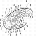
The typical device for clamping wafer 1 ' of the twin grinder of prior art schematically is shown in Fig. 1 and 2.Abrasive wheel 9 ' keeps wafer W independently of one another with hydrostatic pad 11 '.They limit clamping face 71 ' and 73 ' respectively.Abrasive wheel 9 ' is located at the pivot center 67 ' of abrasive wheel the center of the clamp pressure that wafer W produces, and the center of the clamp pressure that hydrostatic pad 11 ' produces wafer is near the WC of the center of wafer.As long as clamping face 71 ' and 73 ' is consistent during grinding (Fig. 1), wafer just remains in the plane (that is, not crooked) and is ground equably by abrasive wheel 9 '.The general discussion of relevant clamping face alignment can be referring to United States Patent(USP) No. 6,652,358.Yet; If becoming, two faces 71 ' and 73 ' do not lined up; The clamp pressure of abrasive wheel 9 ' and hydrostatic pad 11 ' will produce bending moment in wafer W so; Or perhaps the hydrostatic clamping torque, this moment can make near wafer violent bending (Fig. 2) of the overall generation periphery 41 ' of abrasive wheel opening 39 '.This produces the zone of stress high concentration in wafer W.
Clamping face 71 ' and 73 ' do not line up in twin grinding operation to be very general, generally to be by abrasive wheel 9 ' kinetic (Fig. 2) with respect to hydrostatic pad 11 '.Fig. 2 and Fig. 3 schematically illustrate the possible pattern that does not line up.These comprise the combination of three kinds of different modes.In first kind of pattern, abrasive wheel 9 ' produces laterally mobile S (Fig. 2) along the pivot center 67 ' of abrasive wheel with respect to hydrostatic pad 11 ' translation ground.Second kind of pattern is characterised in that abrasive wheel 9 ' produces vertical inclination VT (Fig. 2 and 3) around the horizontal axis X through each abrasive wheel center.Fig. 2 illustrates the combination of first kind of pattern and second kind of pattern.In the third pattern, abrasive wheel 9 ' produces horizontal tilt HT (Fig. 3) around the vertical axis Y through each abrasive wheel center.These patterns are greatly exaggerated to show notion in the drawings; Actual not lining up is less relatively.In addition, each abrasive wheel 9 ' can both be independent of the motion of another abrasive wheel, makes that the horizontal tilt HT of revolver can be different with the horizontal tilt of right side wheel, also is like this for the vertical inclination VT of two abrasive wheels.
Relevant with the design of hydrostatic pad 11 ' by clamping face 71 ' with 73 ' the size that does not line up caused hydrostatic clamping torque.For example; (for example clamp wafer W larger area pad 11 '; The pad that the worksheet area is bigger), pad (that is, keeping wafer very tight) that abrasive wheel pivot center 67 ' distance pad far away is left in the Clamping Center of pad, hydrostatic pad chucking power that wafer is applied is big or the pad with these combination of features generally can cause bigger moment.
In the clamping device 1 ' of the pad 11 ' that adopts prior art (pad of a prior art example shown in Fig. 4); When clamping face 71 ' and 73 ' does not line up; Bending moment in the wafer W is bigger, wafer clamp is got very tight and firm because filled up near 11 ' (comprising the periphery 41 ' of abrasive wheel opening 39 ').Wafer can not be adjusted with the motion of abrasive wheel 9 ', and near wafer aggressive bend (Fig. 2) edge of opening 41 '.Wafer W can not be ground equably, and their produce and do not hope the nanometer topological structure characteristic that occurs, and these characteristics can not be removed through follow-up processed (for example, polishing).Clamping face 71 ' and 73 ' do not line up and can make the wearing and tearing of abrasive wheel 9 ' inhomogeneous yet, this can further impel on the wafer W after the grinding, to produce does not hope the nanometer topological structure characteristic that occurs.
Fig. 5 A and 5B are illustrated in the nanometer topological structure characteristic that not hoping of can on the surface of the wafer W after the grinding, forming when clamping face 71 ' and 73 ' does not line up and wafer bends during grinding operation occurs.These characteristics comprise center vestige (C trace) 77 ' and B ring 79 ' (Fig. 5 A).Center vestige (C trace) 77 ' normally by abrasive wheel 9 ' laterally move that S and the vertical combination of inclination VT cause, and B ring 79 ' normally causes by the combination of laterally moving S and horizontal tilt HT of abrasive wheel.Shown in Fig. 5 B, these two kinds of characteristics 77 ' and 79 ' all have relative bigger peak valley change.Therefore, these characteristics show that the nanometer topological structure of wafer is relatively poor, and can influence the ability of printing micro-circuitry on wafer surface significantly.
This joint is intended to the various aspects of the technology that maybe be relevant with various aspects of the present invention of introducing to the reader, and various aspects of the present invention are described and/or claimed hereinafter.Believe that the discussion at this helps for the reader provides background information, is beneficial to understand better various aspects of the present invention.Therefore, should be appreciated that these narrations will read on this meaning, rather than as the approval to prior art.
Summary of the invention
To be a kind of twin grinder that uses following type carry out the method for processed to semiconductor wafer for aspect, and this grinder remains on wafer between a pair of abrasive wheel and has therein between a pair of hydrostatic pad of hydrostatic pressure.This grinder comprises processor, and this processor comprises that detection drawn the mode detection software of the electric current of getting (draw) by abrasive wheel.This method comprises a plurality of stages, and these stages comprise holding chip, grinding wafers and make wafer and abrasive wheel disengages.This method also comprises to be used said software to detect each stage and is applied to the clamp pressure of wafer in each phasic change hydrostatic pressure with change, improves the nanometer topological structure in the wafer of processed processing thus.
To be a kind of twin grinder that uses following type carry out the method for processed to semiconductor wafer in another aspect, and this grinder is remaining on wafer between a pair of abrasive wheel during the grinding operation and between a pair of hydrostatic pad.The phase I that this method is included in grinding operation is set up the first fluid static pressure with holding chip initially in hydrostatic pad.In the second stage of grinding operation, hydrostatic pressure is reduced to than the second low hydrostatic pressure of first pressure during the wafer grinding.In the phase III of grinding operation, make hydrostatic pressure be increased to the 3rd pressure, and improve the nanometer topological structure in the wafer of processed processing thus with holding chip.
Another aspect is a kind of twin grinder that comprises a pair of abrasive wheel, a processor and a pair of hydrostatic pad again.Abrasive wheel and hydrostatic pad can be operated so that the smooth wafer of cardinal principle is remained in the plane, and wherein the first of wafer is between abrasive wheel, and the second portion of wafer is between hydrostatic pad.Hydrostatic pad comprises through its water that flows through to keep hydrostatic pressure.This grinder also comprises the flow control valve that is used to control the discharge through said pad and controls hydrostatic pressure thus.Flow control valve is controlled by processor.
There are various refinements about the described characteristic of above-mentioned each side.Also can in above-mentioned each side, add further feature.These refinements and supplementary features can exist independently or with any combination.For example, can individually or with any combination following various characteristics about any illustrated embodiment discussion be joined in any above-mentioned each side.
Description of drawings
Fig. 1 is the schematic side elevation of the device for clamping wafer of prior art, comprises hydrostatic pad and abrasive wheel, and semiconductor wafer is between the hydrostatic pad and between the abrasive wheel, and with section hydrostatic pad is shown;
Fig. 2 is the schematic side elevation similar with Fig. 1, but abrasive wheel takes place laterally to move and vertically tilt;
Fig. 3 is the schematic elevational view of device for clamping wafer, and the horizontal tilt of abrasive wheel and vertically inclination are shown;
Fig. 4 is the sketch map of wafer side of one of hydrostatic pad of the prior art of Fig. 1;
Fig. 5 A is to use the device for clamping wafer of Fig. 1 to grind and with after the diagram of the nanometer topological structure surface characteristics of the semiconductor wafer after the polishing;
Fig. 5 B is the diagram of radially profile on surface of the wafer of Fig. 5 A;
Fig. 6 is the schematic side elevation that the grinder of device for clamping wafer of the present invention is housed, and wherein with section hydrostatic pad is shown;
Fig. 7 is the schematic side elevation of amplification of the device for clamping wafer of grinder, comprises hydrostatic pad and abrasive wheel, and semiconductor wafer is between the hydrostatic pad and between the abrasive wheel;
Fig. 8 is the perspective view of the hydrostatic pad on the left side of the present invention, the hydrostatic pocket configuration when being illustrated in grinding operation on the face relative with wafer of this pad;
Fig. 9 A is the wafer side front view of the left hydrostatic pad of Fig. 8, has been shown in broken lines abrasive wheel and wafer, concerns so that they and the position of pad to be described;
Fig. 9 B is the upward view of the hydrostatic pad of Fig. 9 A, and wafer still is shown in broken lines;
Figure 10 is the wafer side front view similar with Fig. 9 A, and the passage that each the fluid inlet in each hydrostatic pocket that makes pad connects is shown;
Figure 11 is the local amplification front elevation of the hydrostatic pad of Fig. 9 A, and the position of hydrostatic pocket with respect to the abrasive wheel opening of pad is shown;
Figure 12 is the perspective view similar with Fig. 8 of right hydrostatic pad, and this right side hydrostatic pad is relative with left hydrostatic pad when grinding operation, makes wafer can remain between two pads;
Figure 13 A is the front view similar with Fig. 9 A of right hydrostatic pad;
Figure 13 B is the upward view of right hydrostatic pad;
Figure 14 is the diagram similar with Fig. 5 A, but illustrates that the device for clamping wafer that uses Fig. 6 grinds and with after the semiconductor wafer after the polishing;
Figure 15 A is the diagram that in process of lapping, when keeping wafer with hydrostatic pad according to the present invention, is applied to the nip stress on the semiconductor wafer surface;
Figure 15 B is the diagram similar with Figure 15 A, and the nip stress that acts on the wafer that keeps with the hydrostatic pad of prior art is shown;
Figure 16 is illustrated in during the grinding stress curve figure near the semiconductor wafer the abrasive wheel periphery when abrasive wheel takes place laterally to move, and to using the wafer that keeps according to hydrostatic pad of the present invention and wafer with the hydrostatic pad maintenance of prior art to compare;
Figure 17 is and the similar curve map of Figure 16 to have compared by the stress in the wafer that laterally moves and vertically tilt to cause of abrasive wheel;
Figure 18 is and the similar curve map of Figure 16, compared laterally to move the stress in the wafer that the combination with horizontal tilt causes by abrasive wheel;
Figure 19 is and the similar curve map of Figure 16, compared by abrasive wheel laterally move, vertically tilt and wafer that the compound action of horizontal tilt causes in stress;
Figure 20 is a curve map, compared wafer that in the device for clamping wafer of prior art, grinds and the wafer that in device for clamping wafer of the present invention, grinds on the nanometer topological structure value of 0.05 percentile (upper 0.05percentile);
Figure 21 is the sketch map of hydrostatic pad according to a second embodiment of the present invention, the hydrostatic pocket configuration when grinding is shown on the face relative with semiconductor wafer of this pad;
Figure 22 is that the part of nanometer topological structure of the present invention system is the schematic elevational view of block diagram form;
Figure 23 is the schematic side elevation of nanometer topological structure evaluating system;
Figure 24 is a curve map, and the output of a plurality of sensors in the nanometer topological structure evaluating system is shown;
Figure 25 A is the sketch map of an example of those positions that can from the clamping conditional information of wafer, draw the boundary condition of finite element analysis;
Figure 25 B illustrates the grid of the finite element structural analysis that is suitable for carrying out wafer;
Figure 26 A and 26B are the nanometer topological structure profiles that utilizes the wafer of nanometer topological structure evaluating system acquisition;
Figure 27 is a curve map, and the prediction profile of wafer according to an embodiment of the invention is shown, and the average radial profile of this wafer after polishing that is obtained by the nanometer surveying instrument is shown; And
Figure 28 is the diagram of the correlation between the B ring actual value of B ring predicted value and the wafer among Figure 27 of the wafer among Figure 27, and coefficient correlation is R=0.9.
Figure 29 is the sketch map of another embodiment of wafer grinder.
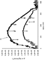
Figure 30 is the curve map that the abrasive wheel of the grinder of Figure 29 draws the electric current of getting.
Figure 31 is the curve map of the standardization distribution that the threshold level area measure value on the wafer surface is shown to former process of lapping and the process shown in Figure 29.
Figure 32 is the case line chart that the standardization threshold level area measure value on the wafer surface is shown to former process of lapping and the process shown in Figure 29.
In each figure, corresponding Reference numeral is represented corresponding part.
The specific embodiment
Accompanying drawing again, Fig. 6 and 7 schematically illustrates according to device for clamping wafer of the present invention, and this clamping device is represented with Reference numeral 1 generally.Said clamping device can be used in the twin grinder, and twin grinder is represented with Reference numeral 3 generally in Fig. 6.Can use the example of the twin grinder of device for clamping wafer 1 to comprise Co., model DXSG320 and model DXSG300A that Ltd. makes by Koyo Machine Industries.In grinder 3, device for clamping wafer 1 remains vertical attitude with single semiconductor wafer (be " workpiece " in a broad sense, totally represent with W in the drawings), makes that two surfaces of wafer can be ground simultaneously equably.This can improve the flatness and the depth of parallelism of wafer surface before polishing and circuit print steps.Should be appreciated that grinder can have the clamping device that keeps other workpiece except that semiconductor wafer and do not depart from the scope of the present invention.
Also shown in Fig. 6 and 7, device for clamping wafer 1 comprises left and right abrasive wheel (representing with Reference numeral 9a and 9b respectively generally) and left and right hydrostatic pad (representing with Reference numeral 11a and 11b respectively generally).Marking a left side is for convenience with the right side, but not any specific orientation of mandatory provision abrasive wheel 9a and 9b and hydrostatic pad 11a and 11b.Letter " a " and " b " is used for the each several part of revolver 9a and left side pad 11a and the each several part of right wheel 9b and the right 11b of pad are distinguished. Abrasive wheel 9a and 9b and hydrostatic pad 11a and 11b adopt mode well known by persons skilled in the art to be installed in the grinder 3.
Also known in the art, two abrasive wheel 9a are identical with 9b essence, and each abrasive wheel is smooth generally.Shown in Fig. 6 and 7, abrasive wheel 9a and 9b roughly are positioned to engage with the wafer grinding towards the lower central of wafer W.The periphery of each abrasive wheel 9a and 9b extends to below the periphery of wafer W in the bottom of wafer W, and extends to above the central axis WC of wafer at the center of wafer.This has guaranteed that the whole surf zone of each wafer W all obtains grinding during operation.In addition, at least one abrasive wheel 9a or 9b can be with respect to the abrasive wheel motions of its pairing.Be convenient between abrasive wheel 9a and the 9b in the clamping device 1 of grinder 3 semiconductor wafer W loaded in place like this.In addition, shown in clamping device 1 in, left hydrostatic pad 11a can be with respect to corresponding left abrasive wheel 9a motion, also can be with respect to keeping fixing right hydrostatic pad 11b motion, semiconductor wafer W is packed in the clamping device 1 further being convenient to.Two pads with respect to the movable device for clamping wafer of corresponding abrasive wheel, or two pads when the loaded with wafers fixing device for clamping wafer, or the device for clamping wafer that moves together during in loaded with wafers of a hydrostatic pad and corresponding abrasive wheel do not depart from the scope of the present invention.
Also see the device for clamping wafer 1 shown in Fig. 6 and 7, during grinding operation, two abrasive wheel 9a of device for clamping wafer and 9b and two hydrostatic pad 11a and 11b are arranged to semiconductor wafer W is clipped in therebetween with relation respect to one another. Abrasive wheel 9a and 9b and hydrostatic pad 11a and 11b limit vertical clamping face 71 and 73 respectively, and on wafer W, produce the clamp pressure that helps wafer is remained its vertical attitude.Hereinafter will be described this point in more detail.
With reference to Fig. 6, it is fixed that hydrostatic pad 11a and 11b keep during operation especially, and the driving ring of representing with Reference numeral 14 generally makes wafer W with respect to hydrostatic pad and abrasive wheel 9a and 9b rotation.As it is known in the art; The pallet of driving ring 14 (or plectrum) 15 roughly on wafer perimeter formed recess N (being shown in broken lines among Fig. 6) engage with wafer W so that wafer is around its central axis WC (central axis WC is roughly corresponding to horizontal axis 44a and the 44b (referring to Fig. 8 and Figure 12) of pad 11a and 11b) rotation.Simultaneously, abrasive wheel 9a and 9b engage with wafer W, and rotate along opposite directions.Abrasive wheel 9a rotates with a direction identical with the wafer W edge among the 9b, and another rotates along opposite direction with wafer.
Referring now to Fig. 8-13B, illustrate in greater detail hydrostatic pad 11a of the present invention and 11b.Fig. 8-11 illustrates left hydrostatic pad 11a, and Figure 12-13B illustrates relative right hydrostatic pad 11b.Can see that from figure two pad 11a are identical with 11b basically, and are roughly mirror image each other.Therefore, will only describe left side pad 11a, but should be appreciated that the description to right side pad 11b is identical.
Shown in Fig. 8-9B, left hydrostatic pad 11a is thinner substantially, and is circular, and its size is similar with the wafer W that will process.The with dashed lines wafer W of having drawn in Fig. 9 A and 9B is to illustrate this relation.The diameter of shown hydrostatic pad 11a is about 36.5cm (14.4in), is about 900cm with the worksheet area that wafer W is faced mutually during operation
2(139.5in
2).Therefore, can be enough it come lapping diameter for example to be about the standard wafer of 300mm.Yet, should be appreciated that hydrostatic pad can have different diameters and surface area and do not depart from the scope of the present invention.For example, the size of hydrostatic pad can be dwindled to be used for grinding the wafer of 200mm.
Can see best that from Fig. 8 and 9A the body 17a of hydrostatic pad 11a is included in during the grinding operation the directly wafer side 19a relative with wafer W.Six hydrostatic pocket 21a, 23a, 25a, 27a, 29a and 31a that on wafer side 19a, form be generally be positioned at separately radially the pad 11a abrasive wheel opening (totally representing) with Reference numeral 39a on every side.The back side 35a opposite of the 17a of pad portion with wafer side 19a be generally put down and do not have hydrostatic pocket, but also can comprise dimple and not depart from the scope of the present invention.In addition, the hydrostatic pad that has greater or less than six hydrostatic pocket (for example, four dimples) does not depart from the scope of the present invention yet.
Each is arc for six hydrostatic pocket 21a, 23a, 25a, 27a, 29a and 31a, and around pad 11a along roughly circumferencial direction elongation.Each dimple 21a, 23a, 25a, 27a, 29a and 31a are recessed in the convex surfaces 32a of wafer side 19a, and comprise the flat vertical sidewall 37a and the circumference corner of rounding separately.These dimples form through in the face 19a of pad 11a, cutting or cast shallow chamber.Forming hydrostatic pocket with different processes does not depart from the scope of the present invention yet.
Still referring to Fig. 8 and 9A, can see that the every couple of dimple 21a and 23a, 25a and 27a and 29a and 31a have same size and shape basically.In addition, shown in pad 11a in, the surface area of dimple 21a and 23a respectively is about 14.38cm
2(2.23in
2); The surface area of dimple 25a and 27a respectively is about 27.22cm
2(4.22in
2); The surface area of dimple 29a and 31a respectively is about 36.18cm
2(5.61in
2).Total pocket surface area of pad 11a is about 155.56cm
2(24.11in
2), total pocket surface area of pad is about 0.17 with the ratio of worksheet area.This ratio can be other value and still within the scope of the invention except that 0.17.For example, this ratio can be about 0.26 or littler.By contrast, in the pad 11 ' (Fig. 4) of prior art, dimple 21 ' and 23 ' surface area respectively are about 31.82cm
2(4.93in
2); Dimple 25 ' and 27 ' surface area respectively are about 36.47cm
2(5.65in
2); Dimple 29 ' and 31 ' surface area respectively are about 47.89cm
2(7.42in
2).Total pocket surface area of the pad 11 ' of prior art is about 232.36cm
2(36.02in
2), the ratio of total pocket surface area and the worksheet area of pad is about 0.26, and (the worksheet area of pad 11 ' is about 900cm
2(139.5in
2)).
Fig. 8 and 9A illustrate the circular abrasive wheel opening 39a in the bottom of the body 17a that is formed on hydrostatic pad 11a, and the size of opening 39a becomes to pass pad with shape set and admits abrasive wheel 9a and make abrasive wheel 9a engage (abrasive wheel and wafer dot in Fig. 9 A) with the lower central of wafer W.When abrasive wheel 9a (and 9b) was received among the opening 39a, the center of opening 39a was corresponding basically with the pivot center 67 of abrasive wheel 9a (and 9b).Shown in pad 11a in, the radius R 1 of abrasive wheel opening 39a is about 87mm (3.43in), the distance between the radially opposed edges 41a of the periphery of abrasive wheel 9a and abrasive wheel opening is more even, generally is about 5mm (0.20in).These distances also can be different within the scope of the invention.
Still as shown in the figure, the convex surfaces 32a of pad 11a comprises (coextensive) the tableland 34a that extends sustained height jointly around the circumference extension of each dimple 21a, 23a, 25a, 27a, 29a and 31a.Be formed with the discharge-channel that each is represented with Reference numeral 36a among the convex surfaces 32a between each tableland 34a of dimple 21a, 23a, 25a, 27a, 29a and 31a.Between the inside part edge 38a of the tableland 34a of the periphery 41a of abrasive wheel opening and dimple 21a, 23a, 25a and 27a, the half moon-shaped free zone 60a that is roughly in the recessed convex surfaces is arranged.The chucking power that 60a acts on the wafer W in the free zone is actually 0.These characteristics will be described hereinafter.
Referring now to Figure 10,, hydrostatic pocket 21a, 23a, 25a, 27a, 29a and 31a respectively comprise fluid are introduced the fluid inlet 61a in the dimple.Passage 63a (shown in the dotted line) in the body 17a of pad is connected to each other with fluid inlet 61a and fluid from outside fluid source (not shown) is supplied to dimple.Fluid is than being pressed under the constant compression force among dimple 21a, 23a, 25a, 27a, 29a and the 31a during work, makes the face 19a contact wafer W of fluid when grinding rather than pad.Like this; The fluid at dimple 21a, 23a, 25a, 27a, 29a and 31a place vertically remains on wafer W in the pad clamping face 73 (seeing Fig. 6 and 7), but still forms lubricated supporting area or the slip barrier that allows wafer W when grinding, to rotate with respect to pad 11a (and 11b) with very little frictional resistance.The chucking power of pad 11a mainly appears at dimple 21a, 23a, 25a, 27a, 29a and 31a place.
Figure 11 illustrates in greater detail the orientation of dimple 21a, 25a and 29a with reference to the left side of the wafer side 19a of pad 11a.Radial distance RD1, RD2 and RD3 represent the peripheral position of dimple 21a, 25a and the 29a vertical sidewall 37a nearest apart from the abrasive wheel open centre (nearest vertical sidewall 37a is meant the vertical sidewall near the edge 41a of abrasive wheel opening 39a) respectively, and said open centre is in theory corresponding to the pivot center 67 of abrasive wheel.As shown in the figure, distance R D1 is non-constant around the nearest vertical sidewall 37a of dimple 21a, and it is farther to make the bottom of dimple 21a leave mouthful 39a than the top.Specifically, distance R D1 changes to about 112mm (4.4in) (these values of dimple 23a are identical) of top end from about 104mm (4.1in) of dimple bottom end position.Divide radial distance RD2 and the RD3 of the nearest vertical sidewall 37a that is clipped to dimple 25a and 29a more constant, wherein, the value of RD2 is about 113mm (4.4in), and the value of RD3 is about 165mm (6.5in) (these values of dimple 27a and 31a are identical respectively).Within the scope of the invention, also can be that radial distance RD1 maintenance is constant, and RD2 and RD3 be non-constant.
Figure 11 also illustrate radially the tableland 34a that measures from abrasive wheel pivot center 67 to dimple 21a and 25a radially inside the radial distance RD11 of edge 38a.Edge 38a limits outward flange or the border of zero pressure district (free zone) 60a.Can find out; Radial distance RD11 to edge 38a is non-constant; And shown in pad 11a in, this radial distance changes to about 87mm (3.43in) that dimple 21a bottom end vicinity is the edge 41a intersection of edge 38a and abrasive wheel opening near the about 108mm (4.25in) the vertical axis 43a.When from the periphery of abrasive wheel 9a (when being received in opening 39a time) to edge 38a radially relatively in portion when carrying out these identical measurements; Measured value changes to about 5mm (0.20in) of the bottom end vicinity of dimple 21a near the about 26mm (1.02in) the vertical axis 43a, and changes to about 0.057 with the ratio of the radius R 1 of abrasive wheel opening 39a from about 0.30.By contrast; Respective in the hydrostatic pad 11 ' of prior art (Fig. 4) is constant because convex surfaces 32 ' in periphery 38 ' overlap (being no zero pressure district (free zone) in the pad 11 ' of prior art) with the edge 41 ' of abrasive wheel opening.In this pad 11 ', radial distance RD11 ' is about 87mm (3.43in), and to the edge 38 ' when carrying out identical measurement, measured value is about 5mm (0.20in) from the periphery of abrasive wheel 9 '.
Figure 15 A-19 illustrates with the stress in the wafer W of the pad 11 ' maintenance of pad 11a of the present invention and 11b and prior art.Figure 15 A and 15B illustrate these stress in clamping face when alignment of abrasive wheel and hydrostatic pad intuitively.In two plates W, the stress in the abrasive wheel opening 39 and 39 ' can ignore (pad in these zones not holding chip).Figure 15 A is illustrated in the less stress that forms in the wafer W that keeps with pad 11a and 11b.This figure illustrates near the whole lip-deep less stress of wafer W abrasive wheel edge of opening 41a and 41b (with the 98 and 99 light color districts that represent) especially.It also shows the stress that is more evenly distributed on wafer.By contrast, shown in Figure 15 B, appear near the periphery (promptly not having zero pressure district (free zone)) of opening 39 ' with the maximum stress 97 in the wafer W of pad 11 ' maintenance.
Comparison diagram 15A and 15B can find out that also that kind was general when the concentration zones 97 of big stress was not so good as to use pad 11 ' (Figure 15 B) during grinding when using pad 11a and 11b.Its benefit is that the local deformation of wafer W near buckled zone (as the edge of abrasive wheel opening 41a) is littler, and the wearing and tearing of abrasive wheel 9a and 9b are more even.The shape of abrasive wheel did not change (abrasive wheel wearing and tearing indifference) when the abrasive wheel wearing and tearing evenly can be guaranteed to grind.This guarantees that also grinder can keep lower nanometer topological structure setting in the long term.In addition, be moved really or tilt, then be distributed in entire wafer W effectively and go up and reduce obvious formation that center vestige (C trace) and B encircle by kinetic stress like abrasive wheel.This such as the people hope ground reduced to grind the sensitiveness that the nanometer topological structure moves and tilts for abrasive wheel.
Figure 16-19 usefulness curve map is illustrated in and uses hydrostatic pad 11a and 11b to carry out during the grinding operation the less stress in the wafer W when abrasive wheel 9a and 9b move and/or tilt.Shown in stress for those near the edge of abrasive wheel opening 41a and 41b, appear in the wafer W, from about 7 o ' clock positions (arc length of 0mm) beginning and around near the periphery measured stress in position edge 41a and the 41b of mobile (to the arc length of about 400mm) clockwise.Stress in the wafer W that keeps with the hydrostatic pad of prior art 11 ' is represented with label 91 generally, representes with label 93 generally with the stress in the wafer of pad 11a and 11b maintenance.
Figure 17 illustrates abrasive wheel and moves the stress 91 and 93 in the wafer W when vertically tilting.Equally, relevant with 11b with pad 11a stress 93 remains unchanged along the whole periphery of abrasive wheel edge of opening 39a and 39b basically.In addition, much little in the wafer W that keeps with pad 11a and 11b in increase corresponding to the stress 93 of the position of center wafer WC.Therefore, when abrasive wheel 9a and 9b move when vertically tilting, near the bending of the wafer W periphery of abrasive wheel opening 39a and 39b be severity so, and the formation of center vestige (C trace) minimizing.
Figure 20 illustrates the nanometer topological structure value with last 0.05 percentile of the wafer of the hydrostatic pad 11 ' of prior art and hydrostatic pad 11a of the present invention and 11b grinding.Use the nanometer topological structure value of the wafer of pad 11 ' grinding to represent with label 72 generally, the nanometer topological structure value of the wafer that use pad 11a and 11b grind is represented with label 74 generally.The nanometer topological structure value 74 of using the pad of the present invention 11a and the wafer of 11b grinding is all the time less than the value 72 of prior art.
The schematically illustrated left hydrostatic pad according to a second embodiment of the present invention of Figure 21.This pad representes with label 111a generally, and this pad adds " 100 " expression with the corresponding part of the part of pad 11a first embodiment with identical label.This hydrostatic pad 111a and above-mentioned hydrostatic pad 11a are roughly the same, but the shape of the hydrostatic pocket 121a that is had, 123a, 125a, 127a, 129a and 131a and orientation are different with 31a with corresponding dimple 21a, 23a, 25a, 27a, 29a in filling up 11a.11a is similar with pad; Dimple 121a, 123a, 125a, 127a, 129a and 131a are radially the location around the abrasive wheel opening 139a of pad 111a, and wherein dimple 121a and 123a, dimple 125a and 127a and dimple 129a and 131a are similar and be symmetrically located on the relative two halves of wafer side 119a.In addition, dimple 121a and 123a along the circumferential direction extend around pad 111a.But in this pad 111a, dimple 125a, 127a, 129a and 131a radially extend away from abrasive wheel opening 139a.These pads 111a is identical with 11b with pad 11a in all others with 111b.
Can expect in addition, can influence the Clamping Center of hydrostatic pad through the pressure of the water of control action on the dimple of hydrostatic pad.This can reduce the Clamping Center, and it is moved the pivot center of the abrasive wheel of smectic holder for x-ray film.More particularly, the fluid pressure in each dimple (or some subclass of dimple) can change and/or be independent of other dimple and controls in process of lapping.Change a kind of method of pressure in some dimples and be and make varying in size of the hole led in these dimples.In addition, in dimple, also can change the hardness in the zone that is associated with each dimple through the degree of depth difference that makes each dimple.Darker dimple is submissiveer to the superficial dimple of the maintenance of wafer W in its zone, and the maintenance to wafer in its zone of more shallow dimple is firmer.
Be described for the wafer W that diameter is about 300mm with described hydrostatic pad 11a, 11b, 111a and 111b shown in this paper.As previously mentioned, within the scope of the invention also the hydrostatic pad that reduces of useful size grind the wafer of 200mm.This also is applicable to the various hydrostatic pad dimensions described in this paper.
According to another aspect of the present invention, the system that is used for assessing the nanometer topological structure begins to provide the feedback to wafer nanometer topological structure when wafer is positioned at twin grinder.Said nanometer topological structure evaluating system comprises at least one sensor, and this sensor arrangement becomes when workpiece is maintained in the twin grinder, to collect with the position of workpiece and/or is out of shape relevant information.Said sensor can carry out one or more measurements, and these measurements are used for limiting the one or more boundary conditions in the finite element structural analysis that is used in wafer.Be to be understood that; This system can only have single-sensor to carry out single measurement; Be used for confirming single boundary condition; This does not depart from the scope of the present invention (as long as there are enough boundary conditions to carry out finite element analysis, comprising any boundary condition that can not use sensor and limit or suppose).Yet in certain embodiments, said one or more sensors carry out a plurality of measurements, are used for limiting a plurality of boundary conditions, and this is to limit the finite element structural analysis that extra boundary condition is used for wafer owing to recognize usually hope (perhaps needing).
For example, an embodiment of schematically illustrated nanometer topological structure evaluating system of the present invention representes with 301 on this overall system in Figure 22 and 23.Although the description of this embodiment has combined to have the twin grinder (as high-visible among Figure 25 A that discussed below and the 25B) of special hydrostatic pad configuration; But should be understood that said nanometer topological structure evaluating system also is suitable for using and not departing from the scope of the present invention with other twin grinder (having the different workpiece grasping system).In addition, the invention is not restricted to said nanometer topological structure system self, but also comprise the twin grinder that has been equipped with nanometer topological structure evaluating system of the present invention.
One or more sensor 303 (for example, a plurality of sensors) is set on the inner surface of hydrostatic pad 305.For example, in specific embodiment shown in the drawings, make the inner working face location (Figure 23) of a plurality of (for example four) sensor 303 along each hydrostatic pad 305.Can use the sensor of any kind, be used to the finite element structural analysis limited boundary condition of wafer as long as it can collect information.For example; In one embodiment; Sensor 303 comprises the dynamic air pressure sensor, and the compressed air stream that this sensor sprays from nozzle through measurement impacts the resistance that on wafer (the E4N type of for example being made by MARPOSS), is run into and measures the distance between hydrostatic pad and the wafer W.Said compressed air is discharged in the atmosphere.This nozzle can be rigidly attached on the hydrostatic pad 305 or otherwise fix with respect to hydrostatic pad.Recognized like the ability technical staff, represented the spacing between hydrostatic pad 305 and the wafer W surface from this dynamic pressure transducer 303 resulting measurement results.Therefore, by the resulting pressure measxurement of dynamic air pressure sensor corresponding to the distance between sensor 303 and the wafer W surface.
The sensor 303 of the nanometer topological structure evaluating system relevant with each hydrostatic pad 305 separates with other related sensor of this hydrostatic pad on the x direction of xyz orthogonal coordinate system (Figure 22 and 23) and at least one direction in the y direction, and wherein said xyz orthogonal coordinate system is defined as to make wafer W to be maintained in the xy plane.In such a way sensor 303 is separated a sensor easy to use and carries out and the lip-deep corresponding measurement in position of wafer W, and use another sensor carry out with wafer surface on the corresponding measurement of another diverse location.
In addition, each hydrostatic pad 305 among the embodiment shown in the drawings all has the sensor 303 of similar number, and the sensor on pad to distribute be the mirror image that the sensor on another pad distributes basically.Therefore, all has the sensor 303 that separates at least one direction in the x of xyz coordinate system direction and y direction on two hydrostatic pad 305.In addition; When hydrostatic pad 305 orientate as that kind shown in figure 23 against each other the time (for example; When grinder in use the time), it is right that sensor 303 is made into, each sensor on one of them hydrostatic pad and certain sensor pairing on another hydrostatic pad.The sensor 303 of sensor centering roughly is in alignment with each other on the x in the xyz coordinate system and the y direction, only on the z direction, separates each other substantially.Each sensor 303 of sensor centering is positioned on the relative both sides of the wafer W that is kept by hydrostatic pad 305, is convenient to like this at same position the relative both sides of wafer measured simultaneously.So just allow to confirm simultaneously the surface location on these wafer W both sides, position.
The quantity of sensor 303 with arrange and can change.Usually; Ability technical staff will appreciate that; It can be favourable adopting the sensor 303 of greater number; Because these sensors can be used to obtain more measurement result and limit more boundary condition, thus the result's of the finite element analysis that reduces in the zone between each boundary condition wafer distortion to be carried out uncertainty.Yet, the number of sensor 303 is also had actual restriction.For example, hope the influence minimum of the holding function of sensor 303 convection cell static(al) pads 305, vice versa.For example, in nanometer topological structure evaluating system 301 shown in the drawings, sensor 303 is arranged on the tableland 311 of hydrostatic pad 305, rather than in hydrostatic pocket 313.(be shown among Figure 25 A with tableland 311 and hydrostatic pocket 313 corresponding positions, this figure is the boundary condition figure that is released from the wafer holder condition.) so between sensor 303 and zone, produce separation by the wafer W of hydrostatic pocket 313 clampings, can from the clamping conditional information, derive boundary condition in this case thus.Separation between sensor 303 and the dimple 313 also can reduce the influence that the local influence of hydrostatic pocket causes sensor measurement.
As stated, sensor 303 different piece that is positioned at wafer W is measured.For example, some sensors 303 are oriented to carry out the measurement relevant with the core of wafer W, and easy formation B encircles and/or the wafer of C trace defective is partly measured and other sensor is positioned at.Referring to the concrete sensor configuration shown in Figure 22 and 23, sensor 303 is positioned at apart from a plurality of different distance place at wafer W center and measures.At least one sensor (a plurality of sensors of the sensor centering of for example being represented by C) is placed in during grinding near the center of wafer W, and this sensor can carry out at this place and the relevant measurement of distortion of center wafer part.At least another sensor (a plurality of sensors of the sensor centering of for example, being represented by R and L) is placed in (that is, comparatively speaking away from center wafer) near the peripheral part of wafer W during grinding.(for example also has another sensor; A plurality of sensors of the sensor centering of representing by U) near near said at least one sensor being positioned at wafer perimeter and be positioned at and be placed in (for example, the wafer part that forms B ring and/or C trace defective easily) on the position apart from wafer W center moderate distance near said at least one sensor the center wafer.
When wafer W is rotated in grinder, receive bending moment do the time spent it can be crooked.So, rotate in grinder along with wafer and change in the distortion meeting of the given position wafer W on the wafer.Sensor 303 not only is positioned on the different distance at wafer W center, measuring, and they also can be positioned on the different RADIALs 323,325,327 that extend out from center wafer.For example, on the identical approximately distance of center wafer, but they are on the different RADIALs sensor to the position of R and L.Sensor to the sensor among the R roughly on a RADIAL 323, and sensor to the sensor among the L roughly on another RADIAL 325, these two RADIALs extend out along different directions from the wafer W center.In addition, sensor to the position of the sensor among C and the U roughly on the 3rd RADIAL 327 that extends along another direction from the wafer W center.In the embodiment shown in the figures, RADIAL 323,325,327 each other basically uniformly-spaced.Like this, RADIAL 323,325,327 forms about 120 ° angle each other.Yet, RADIAL to each other the interval and be provided with sensor different RADIALs number could varyization and do not depart from the scope of the present invention.
In addition, sensor 303 is in different positions with respect to each parts of lapping device.For example, sensor is in the relative both sides of abrasive wheel 9 to the sensor among the R to sensor among the L and sensor.This intersects with abrasive wheel 9 to sensor among the L and perpendicular to the virtual plane 331 (shown in Figure 22) on the xy plane (as defined above) of coordinate system sensor among the R and sensor because contain sensor obviously.Because sensor is positioned as the distance identical approximately apart from the wafer W center to R with sensor among the L, therefore by the pair of sensors of said sensor centering carried out measurement wafer a part through the wafer rotation this part of wafer is turned to another sensor to after by said another sensor to measuring.Yet, possibly be different from by sensor the corresponding measurement that sensor carried out among the L the measurement (result) that sensor carried out among the R by sensor, because wafer W bending possibly take place when in grinder, rotating.
In addition; At least one sensor (for example sensor is to a plurality of sensors among R and the L) is positioned the below of the horizontal center line 341 (Figure 22) of wafer basically, and another sensor (for example sensor is to a plurality of sensors among the U) is positioned the top of the horizontal center line of wafer basically at least.Another sensor (for example sensor is to a plurality of sensors among the C) can be positioned to relatively more the horizontal center line 341 near wafer W.For example, in the embodiment shown in the figures, sensor the sensor among the C is positioned at wafer W horizontal center line 341 lean on last place slightly.
In addition, at least one sensor (for example, sensor is to a plurality of sensors among R, C and the L) is arranged near one of opening 345 of the hydrostatic pad 305 of admitting abrasive wheel 9, therefore be located in during operation abrasive wheel near.Similarly, the position of at least one sensor (for example, sensor is to a plurality of sensors among R, C and the L) than any one hydrostatic pocket 313 all more near abrasive wheel 9.As stated; In some grinders; Not the lining up of grinder can make in the transition part of wafer W between the clamp area of the clamp area of abrasive wheel 9 and hydrostatic pad 305 has higher relatively stress; In this situation, all more all can consider to be used for to line up when taking place than any one hydrostatic pocket 313 wafer with relative higher stress is not partly measured at grinder near any sensor 303 of abrasive wheel and/or contiguous during operation abrasive wheel.On this meaning; Thereby use hydrostatic pocket 313 to move apart hydrostatic pad 305 (as stated) that center that abrasive wheel 9 makes chucking power moves apart abrasive wheel and have some other advantage; Because making it possible to reserve more spaces, this configuration of hydrostatic pocket make the sensor 303 in the nanometer topological structure evaluating system 301 be placed in (for example, in the free zone that chucking power is substantially zero) between hydrostatic pocket and the abrasive wheel.
At least the opening 345 of the position of another sensor (for example, sensor is to a plurality of sensors among the U) in the hydrostatic pad 305 is therefore just farther from abrasive wheel 9 during operation.Said at least one sensor (for example, sensor is to a plurality of sensors among the U) also than at least some hydrostatic pocket 313 further from abrasive wheel 9.In addition; (for example can consider said at least one sensor; Sensor is to a plurality of sensors among the U) be positioned in those grinders when grinder taking place not lining up the part of wafer W with relatively low stress is measured; Wherein, these grinders have higher relatively stress in the transition part that takes place can to make when grinder does not line up wafer between the clamp area of the clamp area of abrasive wheel and hydrostatic pad.
As stated, sensor 303 can detect about the information of sensor to the distance on wafer W surface.Sensor 303 links to each other (Figure 22) with the transmission signal with processor 351, processor can receive from the sensing data of sensor output.Processor 351 can be away from lapping device, but this is not necessary.The hardwired 353 of connection processing device 351 and sensor although Figure 22 has drawn should be understood that processor and sensor also can carry out radio communication and do not depart from the scope of the present invention.
CPU in the computer workstation can be used as processor 351.In addition, to can between a plurality of processing units, distributing from the data of sensor 303 and/or to the processing of the information 355 that therefrom obtains, in this situation, term " processor " has comprised the processing unit that all are such.In one embodiment of the invention, processor 351 is monitored the sensing data of exporting from sensor 303 during grinding operation.Can the output of sensor 303 be noted, be used for the operation that information is collected purpose and/or research grinder.If necessary, can during grinding operation and/or afterwards, show with the output of figure with sensor 303, shown in figure 24.
In one embodiment of the invention, processor 351 can use the finite element structural analysis that carries out wafer W from the monitored sensing data of sensor 303.Shown in figure 24, during grinding operation, preferably in the fast end of main grinding stage (for example, before the completion stage of grinding begins), processor 351 is in the moment 357 collecting sensor data.Main milling cycle is corresponding to second step shown in Figure 24.Complete milling cycle shown in Figure 24 comprises 5 quick traverse feeds of step: step 361=(fast infeed); Step 363=master milling cycle; Step 365=is milling cycle at a slow speed; Step 367=sparking out (spark-out) cycle; With step 369=abrasive wheel back-off period.Processor 351 can be confirmed one or more boundary conditions from sensing data, and uses the said one or more boundary conditions that obtain from sensing data to carry out the finite element analysis of wafer W.Add other boundary condition that obtains from the clamping conditional information that produces by hydrostatic pad from the boundary condition that sensing data obtains.The moment that 351 pairs of used data of finite element structural analysis of milling cycle and processor are collected can change and not depart from the scope of the present invention.
Figure 25 A illustrates an example of one group of position, can access the boundary condition about said one group of position from the clamping conditional information.In Figure 25 A, hydrostatic pad 305 around and hydrostatic pocket 313 around the limited boundary condition.Figure 25 B illustrates the grid of the finite element structural analysis that is suitable for carrying out wafer W.Notice that employed hydrostatic pad 305 is compared with above-mentioned hydrostatic pad 11a, 11b and had different fluids static(al) dimple configuration slightly in Figure 25 A and the example shown in the 25B.Yet ability technical staff knows and how to confirm boundary condition and form the grid that is suitable for employed particular fluid static(al) pad in any grinder.
The boundary condition that use obtains from sensing data is together with the boundary condition that obtains from the clamping condition; And the characteristic of wafer W (for example; The material behavior of silicon), processor 351 carries out the shape of the finite element analysis of wafer with prediction of wafer, comprises the prediction of wafer nanometer topological structure.The shape of the wafer W of in finite element analysis, being predicted by processor 351 is the thick profile of wafer.Because process of lapping makes nanometer topological structure characteristic present radial symmetry usually, so the thick profile of wafer can represent with distortion, and distortion is the function to the distance of center wafer.The use sensing data is shown among Figure 26 A through an example of the thick profile of wafer that finite element analysis is predicted.
In one embodiment, use finite element analysis following to the calculating of morphotropism plate shape.In order to carry out this analysis, confirm to adopt the grid of shell unit (shell elements).Figure 25 A illustrates the details of a grid.Should be kept in mind that inclination and situation of movement according to wafer holder angle, abrasive wheel, wafer distortion maybe be bigger at R or L " B ring " sensor place.Big more distortion and NT worsen related just trend towards strong more.Therefore, in order to obtain this effect, higher reading among two reading R and the L is applied to this two positions.Utilize substrate rigidity boundary condition to simulate the clamping of hydrostatic pad to wafer.Polishing NT calculates to the back, and the time spent is less than 10 seconds usually.Consider the displacement of wafer along abrasive wheel periphery (the arc ABC among Figure 25 B).For each radius r that extends out from center wafer, two points are arranged along said arc.Result based on finite element analysis can confirm the displacement at these two some places, and with it on average to produce the average displacement of this radius.Said average displacement can be drawn as thick contour curve (Figure 26 A).Then, the reading that makes thick contour curve is through spatial filter, to produce the contour curve (Figure 26 B) through filtering.
Ability technical staff can be appreciated that, after grinding, has other processing of wafers step usually.For example, after grinding, usually wafer is polished.In addition, not to confirm nanometer topological structure output (nanotopology yield) by the nanometer topological structure after accomplishing after grinding but by downstream step (these steps change the nanometer topological structure of wafer usually).Like this, in one embodiment of the invention, the thick profile of wafer that obtains in processor 351 finite element analyses capable of using predicts what kind of the nanometer topological structure of wafer after one or more downstream steps is likely.
For example, can spatial filter be applied to the thick profile of wafer and predict one or more downstream steps (for example, polishing) wafer profile afterwards.Ability technical staff can the very familiar various wafer defect/output management Software tools that can be used for carrying out this space filtering.Some examples comprise: SiGlaz (Santa Clara, dysnusia analysis CA) (Intelligent Defect Analysis) software; Zenpire (Palo Alto, iFAB software CA); Galaxy Semiconductor Inc.-USA (Waltham, Examinator software MA); With Knights Technology (Sunnyvale, Yieldmanager software CA).What kind of the nanometer topological structure is likely after the wafer profile of filtering is illustrated in further processing.Figure 26 B illustrates an example through the wafer profile of filtering.Wafer for some; The nanometer topological structure measurement result (for example using nanometer surveying instrument
) of the reality of (for example after the polishing) after thick profile of the resulting wafer of finite element analysis and the downstream is compared; Can be (for example to employed parameter in the finite element analysis; The boundary condition relevant) carry out meticulous adjustment, to obtain better association with the hydrostatic clamping.
In addition, processor 351 can be assessed the nanometer topological structure of workpiece from sensor receiving sensor data and by these sensing datas.In one embodiment; Processor can (for example provide information 355 alternatively; The prediction NT of workpiece); So that according to the negative assessment of nanometer topological structure (for example, when one or more wafer profiles fall short of specifications or other predetermined standard time by the determined negative assessment of processor) adopt remedial measures.Its simplest form is, the information 355 that relates to remedial measure can comprise to one or more operating personnel (for example process engineer) output signal, show need adjust and/or process of lapping needs carefully.Signal in response to from processor 351; The alignment that operating personnel can adjust grinder (for example; The angle corresponding with the horizontal tilt of abrasive wheel, with tilt in the moving between corresponding angle and the abrasive wheel at least one of abrasive wheel vertical) and/or adjust the fluid pressure in the dimple that supplies to hydrostatic pad, to improve the grinder performance.As replacement or additional, operating personnel also can adjust alignment through the initial setting up (for example, the rule of thumb of setting) of regulating grinder.Processor 351 also can provide out of Memory 355 to realize some remedial measures, comprises regulating the grinding technics variable.For example; Processor 351 can provide information 355; Be used for showing the position or the application of at least one abrasive wheel and/or hydrostatic pad are adjusted, and/or need come the center of the chucking power of corrective action on wafer through the pressure that adjustment supplies to the fluid in the dimple 313 according to the sensing data needs.Equally, processor 351 can respond operating personnel's input, and to control one group of actuator (not shown), the position that these actuators are used for adjusting at least one abrasive wheel 9 and hydrostatic pad 305 is so that align grinder again.
In an embodiment according to the processing and treating method of semiconductor wafer of the present invention, semiconductor wafer W packed into to be had in the twin grinder of above-mentioned nanometer topological structure evaluating system 301.Except being mentioned here, the actual grinding of wafer W is carried out in a usual manner.In process of lapping, said one or more sensors 303 are collected data, and these data show the distortion of wafer W and can be used to draw the employed one or more boundary conditions of finite element structural analysis of wafer.For example, the sensor 303 of above-mentioned nanometer topological structure evaluating system 301 is collected the surface of wafer W and a plurality of range measurements between the sensor.In addition, the sensor 303 of nanometer topological structure evaluating system 301 is collected data simultaneously from the different piece of wafer and at each diverse location with respect to the grinder parts, as stated.
In one embodiment; Two surfaces of sensor measuring workpieces in the workpiece part relevant with B ring defective apart from aspect deviation, processor 351 can receive this range data and encircle defective by the B the received sensing data assessment workpiece nanometer topological structure from these sensors.In another embodiment; Two surfaces of sensor measuring workpieces in the workpiece relevant part with C trace defective apart from aspect deviation, processor 351 can receive this range data and by the C trace defective the received sensing data assessment workpiece nanometer topological structure from these sensors.
In another embodiment, remedial measure comprises the grinding of adjustment back workpiece.For example, grinder can grind unit one earlier, after having ground unit one, grinds second workpiece then.Processor 351 can receive data and by the nanometer topological structure of these sensing datas assessment unit ones from sensor.Afterwards, processor 351 can provide information 355, and this information shows according to sensing data to be adjusted for when grinding the workpiece (like second workpiece) of back, using the position of at least one abrasive wheel and/or hydrostatic pad.At workpiece is under the situation of several wafers of box, can carry out finite element analysis to each wafer in this box, need not wait until that whole box wafer was all ground after.If if be provided with improper and in one or more wafers, detect the NT defective, other wafer in the box has similar or identical defective so probably, there are not the words of the interference of certain form can cause bigger output loss.According to one embodiment of present invention, all wafers that operating personnel needn't wait from box obtains feedback, has avoided a large amount of output losses.Therefore, provide during grinding afterwards polishing the reliable prediction of NT defective.It is the wafer and the wafer optimized grinder setting that becomes box of back that this prediction helps operating personnel, makes that nanometer topological structure defective is minimum after the wafer polishing of back.
The curve map of Figure 27 illustrates according to an embodiment of the invention the prediction profile for a particular wafer, and illustrates by the average radial displacement profile (average radial displacement profile) of determined this same wafer of nanometer surveying instrument after polishing.Solid line illustrates according to an embodiment of the invention an example of the prediction profile of the wafer that obtains based on finite element analysis.Be shown in dotted line based on from the data of the nanometer surveying instrument that wafer is analyzed and the profile that obtains.Figure 28 illustrates being drawn in the B ring predicted value on the transverse axis and being drawn in the association between the B ring actual value on the longitudinal axis of several wafers, and coefficient correlation is R=0.9.
Method of the present invention provides the quick feedback to the nanometer topological structure performance of grinder.For example,, the wafer milling cycle just can begin to carry out the assessment of wafer nanometer topological structure before accomplishing.In addition, before polishing, just can obtain nanometer topological structure feedback.By contrast, the nanometer topological structure reponse system of many routines adopts laser to check the nanometer topological structure of measuring wafer.These systems can not be used to lack the not polished wafer of reflecting surface usually compatiblely.Ability technical staff can recognize through obtainable many other advantages of method of the present invention according to content of the present disclosure.
In said method, sensor 303 is collected data basically continuously during grinding operation.Yet should be understood that can be after grind accomplishing and wafer is collected data from sensor still in grinder the time.In addition, sensor 303 can be measured off and on or in the single moment, and this does not depart from the scope of the present invention.Similarly, after grinding operation is accomplished and/or in the processing that wafer can be begun to carry out or proceed sensing data after grinder takes out, this does not depart from the scope of the present invention.
In addition; The embodiment of shown above-mentioned nanometer topological structure evaluating system assesses its nanometer topological structure when wafer is remained in the twin grinder vertically; But be understood that; Nanometer topological structure evaluating system also can carry out the assessment of nanometer topological structure to the wafer that is retained as different orientation (for example level), and this does not depart from the scope of the present invention.
Although carrying out finite element analysis to each wafer, the embodiment of the nanometer topological structure evaluating system described in the literary composition assesses its nanometer topological structure; Yet ability technical staff will appreciate that; Can use from the empirical data that this finite element analysis obtained of some and come the formation standard, make processor unactually to carry out finite element structural analysis and just can assess the nanometer topological structure.For example; If the sensing data of the wafer in the grinder enough is similar to the sensing data of another wafer that carried out finite element analysis; The result of so, previous finite element analysis can be used to assess the nanometer topological structure of the wafer in the grinder and needn't carry out finite element analysis to the wafer in the grinder is actual.Database and learning program can be used to this process of reinforcement, have have therefore just reduced or eliminated the situation that processor carries out finite element analysis.Also can imagine; The operating personnel of experienced nanometer topological structure evaluating system can turn out such ability; Promptly; Show or other shows the sign of discerning expression nanometer topological structure defective through the figure of checking sensor output, and manually enforcing remedies measure, this does not depart from the scope of the present invention.
In addition, needn't all carry out the assessment of nanometer topological structure to each wafer.If necessary, can assess the nanometer topological structure to the part in the wafer that in grinder, grinds (for example, being used for the sample of quality control), this does not depart from the scope of the present invention as described hereinly.
Referring to schematic Figure 29, illustrate and on the whole with 500 represent the wafer grinder another embodiment.This wafer grinder totally comprises first fluid static(al) pad 506 and second hydrostatic pad 508 of relatively locating with first fluid static(al) pad.Wafer 501 (being " workpiece " more in a broad sense) is positioned at hydrostatic pad 506, between 508.Also comprise a pair of abrasive wheel (not shown) in this wafer grinder.This wafer grinder can be similar to above-mentioned those embodiment.Yet the wafer grinder of Figure 29 comprises other parts, to help to reduce the NT deterioration of being ground mach wafer by wafer.
The flow of the water of first fluid static(al) pad 506 is led in 504 controls of first flow control valve, and the flow of the water of second hydrostatic pad 508 is led in 502 controls of second flow control valve.In this embodiment, the hydrostatic pressure in the pad is controlled by discharge, but also can imagine other pattern.
Flow control valve the 502, the 504th can be controlled the flow of water or any suitable valve of pressure.For example, flow control valve 502,504 can be globe valve, ball valve, gate valve, diaphragm valve, needle-valve or their any combination.Flow control valve 502,504 can be controlled by any suitable actuator (not shown), and they can be separated control.
The operation of control system 600 control wafer grinders and flow control valve 502,504.Control system 600 comprise have processor, the calculation element 602 of the computer-readable medium of one or more forms and input/output device.In certain embodiments, the processor of calculation element 602 can be operated with control flow control valve 502,504.Control system 600 can operate to measure the amount of the employed electric current of abrasive wheel.The employed electric current of abrasive wheel can directly be measured by control system 600, and perhaps it can receive signal or other communication from the independent supervising device (not shown) of measuring the employed electric current of abrasive wheel.
The scale of the employed electric current of abrasive wheel shows the current generation of grinding operation.For example, and shown in figure 30, when abrasive wheel is at first touched wafer 501, abrasive wheel draw the electric current of getting (draw) with 550 original states represented with increase a little with the 540 remaining compared represented.Figure 30 illustrates each abrasive wheel and during grinding operation, draws the electric current of getting.Electric current draws to be got along with abrasive wheel is attempted holding chip 501 and continue increasing, as along with shown in 560 parts represented.In this stage, less from the material that wafer 501 is removed.Reach its peak value along with electric current draws to be taken at 570 parts represented, the quantity of material of removing from wafer 501 increases.Electric current draws and is taken at most materials and when wafer 501 is removed, is rested on this peak level by abrasive wheel.With 580 no-spark stages (when abrasive wheel begins rollback) of representing, electric current draws gets quick decline.After the complete rollback of abrasive wheel, electric current draws the remaining level of representing with 590 of falling of fetching.
The electric current of the abrasive wheel that calculation element 602 use institutes monitor or sense draws the current generation of fetching prediction (i.e. detection or definite) grinding operation.Calculation element 602 is made this prediction by means of the mode detection software program.This mode detection software program comprises the executable instruction of computer on the computer-readable medium that is stored in said one or more forms on the calculation element 602.The executable instruction of computer is carried out by the processor of calculation element 602.
In one or more grinding stage of removing most materials from wafer 501, therefore control system 600 control flow control valves 502,504 are input to the water of hydrostatic pad 506,508 with reduction flow also reduces the pressure in the hydrostatic pad.During this grinding stage, abrasive wheel supporting wafer 501 and with wafer holder between abrasive wheel.Through during this grinding stage, reducing the pressure in the hydrostatic pad 506,508, reduce or eliminated the amount of the strain that wafer stood greatly.This reducing or eliminating of the strain in the wafer 501 makes the lip-deep NT of wafer 501 reduce.
In operation, control system 600 carries out thus and in square frame 610, uses mode detection software to detect the method that (promptly confirming) grinds the stage.In square frame 620, according to variation by mode detection software detected grinding stage calculated flow rate in square frame 610.Control system 600 uses these variations through control flow control valve 502,504 then in square frame 630.Therefore control system 600 can operate with the regulation and control hydrostatic pressure.
According to another kind of method, control system 600 carries out and comprises holding chip, grinding wafers and make wafer and abrasive wheel disengages the method in these stages.Wafer is maintained in the vertical basically plane.The hydrostatic pressure that mode detection software is used to detect each stage of grinding operation and changes each stage is applied to the clamp pressure of wafer with change, improves the nanometer topological structure in the wafer of being processed thus.The hydrostatic pressure of this embodiment changes through the flow that changes through flow control valve 502,504, but also can imagine the mode that other changes pressure.In the exemplary embodiment, pressure reduced in the grinding stage.In other embodiments, pressure raise during the grinding stage.
Example
Obtain two groups of data through the surface of measuring first group of wafer and second group of wafer.The wafer of being tested does not get into and leaves vestige or other similar defective.Grind first group of wafer according to the common process that during the grinding stage, does not change hydrostatic pressure (being recording process or POR).Embodiment according to during the grinding stage, improving Figure 29 of hydrostatic pressure grinds second group of wafer.Measure the surface (being the THA1010 measurement standard) of the wafer of being tested according to the threshold level mean value of the each several part (for example 10mm * 10mm part) on surface.The vertical distance of maximum peak valley in the part of wafer surface is represented in the measurement of carrying out according to the THA1010 measurement standard.Stride the surface of wafer in different piece (but these parts can be overlapping) and carry out repeatedly such measurement.The THA1010 measurement standard is the known measurement standard that is used for estimating the nanometer topological structure of wafer surface.Use this standard, quantity is low more, and the nanometer topological structure of wafer surface is just good more.
Figure 31 illustrates the curve map that standardization that the THA1010 of two groups of data measures distributes.First group of data is called as standardization THA1010POR, and second group of data is called as standardization THA1010Low Pr.Make the measured value standardization (promptly divided by common divisor) of each group data.The y coordinate of each data point on this curve map representes to be equal to or less than the percentage of measured value of the x coordinate at respective counts strong point.In addition, solid line is represented the boundary of 95% confidential interval of first group of data.Dotted line is represented the boundary of 95% confidential interval of second group of data.
Figure 32 is the case line chart that the lip-deep standardized threshold level area measure value of institute's testing wafer is shown.This illustrates the case line of two groups of data of Figure 31, and this figure illustrates corresponding minimum of a value, first quartile, median, the 3rd quartile and maximum to each group data.
Figure 31 and 32 illustrates the peak valley measured value that has the surface that is significantly less than the wafer that grinds according to POR according to the surface of the wafer of the embodiment grinding of Figure 29 thus.The nanometer topological structure with improvement is compared with the surface of the wafer that grinds according to POR in the surface of the wafer that grinds according to the embodiment of Figure 29 therefore.For example, the wafer that grinds according to the technology of Figure 29 has 0.6346 standardization average T HA1010, and has 0.6738 standardization average T HA1010 according to the wafer that POR grinds.Compare with the wafer (standard deviation=0.09956) that grinds according to POR, standard deviation reduces equally for the wafer (standard deviation=0.09826) that grinds according to Figure 29.
In addition, those of the case line chart of Figure 32 standardization peak valley measured value that the wafer that grinds according to Figure 29 is shown and POR are compared and are distributed in the narrower scope.Shown in clear, the first and the 3rd quartile of second group of data (being Low Pr) is more closely more spaced apart than those of first group of data (being POR Pr).In addition, the maximum of second group of data and minimum of a value have maximum and the low value of minimum of a value than first group of data.
When introducing each key element of the present invention or its preferred embodiment, article " ", " being somebody's turn to do " and " said " are used for expression has one or more key elements.Term " comprises ", " comprising " and " having " be meant included and expression other key element except that listed key element arranged.
Owing to can make various changes to above content within the scope of the invention, therefore be included in above explanation neutralization and show that it is illustrative rather than restrictive that in the accompanying drawings all the elements should be interpreted as.
Claims (20)
1. the twin grinder of the following type of use carries out the method for processed to semiconductor wafer; Said grinder remains on wafer between a pair of abrasive wheel and has therein between a pair of hydrostatic pad of hydrostatic pressure; Said grinder comprises processor; This processor comprises that detection draws the mode detection software of the electric current of getting by said grinder, and said method comprises a plurality of stages, and said a plurality of stages comprise:
Holding chip,
Grinding wafers and
Wafer and abrasive wheel are disengaged,
Use said software to detect each stage and be applied to the clamp pressure of wafer with change, improve the nanometer topological structure in the wafer of processed processing thus in the said hydrostatic pressure of each phasic change.
2. method according to claim 1 wherein, changes said hydrostatic pressure through the flow that changes through flow control valve.
3. method according to claim 1, wherein, said mode detection software measurement is drawn the electric current got to detect each stage by said grinder.
4. method according to claim 1 also is included in and reduces said hydrostatic pressure during the grinding stage.
5. method according to claim 1 also is included in the said hydrostatic pressure that raises during the grinding stage.
6. a twin grinder that uses following type carries out the method for processed to semiconductor wafer, and said grinder is remaining on wafer between a pair of abrasive wheel during the grinding operation and between a pair of hydrostatic pad, said method comprises:
In the phase I of grinding operation, in hydrostatic pad, set up the first fluid static pressure with holding chip initially,
In the second stage of grinding operation, hydrostatic pressure is reduced to than the second low hydrostatic pressure of first pressure during the wafer grinding, and
In the phase III of grinding operation, make hydrostatic pressure be increased to the 3rd hydrostatic pressure, and improve the nanometer topological structure in the wafer of processed processing thus with holding chip.
7. method according to claim 6, wherein, said the 3rd hydrostatic pressure is substantially equal to said first fluid static pressure.
8. method according to claim 6, wherein, wafer is basically by the abrasive wheel clamping during wafer grinds.
9. method according to claim 6, wherein, the use traffic control valve changes hydrostatic pressure.
10. method according to claim 6, wherein, wafer is maintained in the vertical basically plane.
11. method according to claim 6 also comprises the amount of measurement by the employed electric current of abrasive wheel of said twin grinder.
12. method according to claim 11 also comprises the stage of confirming grinding operation based on the amount of the measured employed electric current of abrasive wheel by said twin grinder.
13. method according to claim 12 also comprises when measured electric current and confirms that when remaining state increases to original state the stage of grinding operation is the said phase I.
14. method according to claim 12 comprises that also the stage of when measured electric current is in its peak level, confirming grinding operation is said second stage.
15. method according to claim 14 also comprises when measured electric current and when its peak level reduces, confirms that the stage of grinding operation is the said phase III.
16. twin grinder; Comprise a pair of abrasive wheel, a processor and a pair of hydrostatic pad; Abrasive wheel and hydrostatic pad can be operated so that the smooth wafer of cardinal principle is remained in the plane; Wherein the first of wafer is between abrasive wheel, and the second portion of wafer is between hydrostatic pad, and hydrostatic pad comprises through its water that flows through to keep hydrostatic pressure; Said grinder comprises also and is used to control the flow control valve of also controlling hydrostatic pressure through the discharge of said pad thus that flow control valve is controlled by processor.
17. grinder according to claim 16; Wherein, Processor comprises the mode detection software in each stage that is used to detect process of lapping, and processor can be operated to control the discharge through said flow control valve in response to the stage that is gone out by said mode detection software detection.
18. grinder according to claim 17, wherein, processor can be operated to measure the amount by the employed electric current of abrasive wheel.
19. grinder according to claim 18, wherein, said mode detection software detects the said stage based on the measured amount by the employed electric current of abrasive wheel.
20. grinder according to claim 19, wherein, processor is controlled said flow control valve, increases the discharge through said valve during the stage with the grinding of arriving said process of lapping in said mode detection software detection.
Applications Claiming Priority (3)
| Application Number | Priority Date | Filing Date | Title |
|---|---|---|---|
| US31791910P | 2010-03-26 | 2010-03-26 | |
| US61/317,919 | 2010-03-26 | ||
| PCT/IB2011/051152 WO2011117792A1 (en) | 2010-03-26 | 2011-03-18 | Hydrostatic pad pressure modulation in a simultaneous double side wafer grinder |
Publications (1)
| Publication Number | Publication Date |
|---|---|
| CN102844151A true CN102844151A (en) | 2012-12-26 |
Family
ID=44657008
Family Applications (1)
| Application Number | Title | Priority Date | Filing Date |
|---|---|---|---|
| CN201180016139XA Pending CN102844151A (en) | 2010-03-26 | 2011-03-18 | Hydrostatic pad pressure modulation in a simultaneous double side wafer grinder |
Country Status (8)
| Country | Link |
|---|---|
| US (1) | US8712575B2 (en) |
| EP (1) | EP2552644A4 (en) |
| JP (1) | JP6013317B2 (en) |
| KR (1) | KR101694574B1 (en) |
| CN (1) | CN102844151A (en) |
| SG (1) | SG184014A1 (en) |
| TW (1) | TWI520202B (en) |
| WO (1) | WO2011117792A1 (en) |
Cited By (9)
| Publication number | Priority date | Publication date | Assignee | Title |
|---|---|---|---|---|
| CN105881213A (en) * | 2014-09-01 | 2016-08-24 | 曾庆明 | Precision double-face grinder controller |
| CN105881195A (en) * | 2015-02-17 | 2016-08-24 | 光洋机械工业株式会社 | Double-head plane grinding device |
| CN108127560A (en) * | 2017-12-08 | 2018-06-08 | 中国兵器科学研究院宁波分院 | For the control system of the two-sided fast polishing of square optical element |
| CN108475627A (en) * | 2015-11-26 | 2018-08-31 | 胜高股份有限公司 | Polishing wafer method |
| CN112930248A (en) * | 2019-04-01 | 2021-06-08 | 株式会社村田制作所 | Polishing agent supply device, polishing device, and polishing agent supply method |
| CN113396030A (en) * | 2018-12-27 | 2021-09-14 | 胜高股份有限公司 | Double-end grinding method |
| CN114227524A (en) * | 2021-12-30 | 2022-03-25 | 西安奕斯伟材料科技有限公司 | Double-side polishing apparatus and double-side polishing method |
| CN115070604A (en) * | 2022-06-09 | 2022-09-20 | 西安奕斯伟材料科技有限公司 | Double-side polishing apparatus and double-side polishing method |
| CN115723035A (en) * | 2022-09-08 | 2023-03-03 | 西安奕斯伟材料科技有限公司 | System and method for monitoring processing state of grinding device and double-sided grinding device |
Families Citing this family (5)
| Publication number | Priority date | Publication date | Assignee | Title |
|---|---|---|---|---|
| US9358660B2 (en) | 2011-11-07 | 2016-06-07 | Taiwan Semiconductor Manufacturing Company, Ltd. | Grinding wheel design with elongated teeth arrangement |
| US9960088B2 (en) * | 2011-11-07 | 2018-05-01 | Taiwan Semiconductor Manufacturing Company, Ltd. | End point detection in grinding |
| JP6197580B2 (en) * | 2013-10-29 | 2017-09-20 | 株式会社Sumco | Double-side polishing machine for carrier plate and workpiece |
| JP6513174B2 (en) * | 2017-12-25 | 2019-05-15 | 信越半導体株式会社 | Design method of wafer holding carrier |
| US11415971B2 (en) | 2020-02-10 | 2022-08-16 | Globalwafers Co., Ltd. | Systems and methods for enhanced wafer manufacturing |
Citations (5)
| Publication number | Priority date | Publication date | Assignee | Title |
|---|---|---|---|---|
| US20050260922A1 (en) * | 2004-05-21 | 2005-11-24 | Mosel Vitelic, Inc. | Torque-based end point detection methods for chemical mechanical polishing tool which uses ceria-based CMP slurry to polish to protective pad layer |
| US20060009125A1 (en) * | 2002-10-09 | 2006-01-12 | Kenji Okura | Both side grinding method and both side grinder of thin disc-like work |
| CN1933940A (en) * | 2004-03-19 | 2007-03-21 | Memc电子材料有限公司 | Wafer clamping device for a double side grinder |
| JP2007096015A (en) * | 2005-09-29 | 2007-04-12 | Shin Etsu Handotai Co Ltd | Double-disk grinding apparatus for semiconductor wafer, static pressure pad and double-disk grinding method using the same |
| US20070179660A1 (en) * | 2006-01-30 | 2007-08-02 | Memc Electronic Materials, Inc. | Double side wafer grinder and methods for assessing workpiece nanotopology |
Family Cites Families (32)
| Publication number | Priority date | Publication date | Assignee | Title |
|---|---|---|---|---|
| JPH1177497A (en) * | 1997-09-01 | 1999-03-23 | Waida Seisakusho:Kk | Both faces grinding method of semiconductor wafer and both faces grindings device |
| JPH11154655A (en) * | 1997-11-21 | 1999-06-08 | Komatsu Electron Metals Co Ltd | Manufacture of semiconductor wafer |
| JP3328193B2 (en) * | 1998-07-08 | 2002-09-24 | 信越半導体株式会社 | Method for manufacturing semiconductor wafer |
| JP3664593B2 (en) * | 1998-11-06 | 2005-06-29 | 信越半導体株式会社 | Semiconductor wafer and manufacturing method thereof |
| KR100642879B1 (en) * | 1999-05-07 | 2006-11-10 | 신에쯔 한도타이 가부시키가이샤 | Method and device for simultaneously grinding double surfaces, and method and device for simultaneously lapping double surfaces |
| US6294469B1 (en) * | 1999-05-21 | 2001-09-25 | Plasmasil, Llc | Silicon wafering process flow |
| JP2002307303A (en) * | 2001-04-10 | 2002-10-23 | Koyo Mach Ind Co Ltd | Both face grinding method for thin plate disclike workpiece and device thereof |
| JP2002307275A (en) * | 2001-04-16 | 2002-10-23 | Sumitomo Heavy Ind Ltd | Processing system and chamfering device |
| JP2002346924A (en) * | 2001-05-29 | 2002-12-04 | Sumitomo Heavy Ind Ltd | Work holder |
| JP3848120B2 (en) * | 2001-10-12 | 2006-11-22 | 住友重機械工業株式会社 | Work grinding machine |
| JP2004072076A (en) * | 2002-06-10 | 2004-03-04 | Nikon Corp | Exposure device, stage unit and method for manufacturing device |
| JP3993856B2 (en) * | 2004-01-22 | 2007-10-17 | 光洋機械工業株式会社 | Double-head surface grinding machine |
| JP4326974B2 (en) * | 2004-01-30 | 2009-09-09 | コマツNtc株式会社 | Wafer grinding apparatus and grinding method |
| DE102004005702A1 (en) * | 2004-02-05 | 2005-09-01 | Siltronic Ag | Semiconductor wafer, apparatus and method for producing the semiconductor wafer |
| JP4615275B2 (en) * | 2004-09-21 | 2011-01-19 | 株式会社ディスコ | Wafer polishing apparatus and wafer polishing method |
| JP4752475B2 (en) * | 2005-12-08 | 2011-08-17 | 信越半導体株式会社 | Semiconductor wafer double-head grinding apparatus, hydrostatic pad and double-head grinding method using the same |
| US7662023B2 (en) * | 2006-01-30 | 2010-02-16 | Memc Electronic Materials, Inc. | Double side wafer grinder and methods for assessing workpiece nanotopology |
| MY149762A (en) * | 2006-01-30 | 2013-10-14 | Memc Electronic Materials | Double side wafer grinder and methods for assessing workpiece nanotopology |
| US7930058B2 (en) * | 2006-01-30 | 2011-04-19 | Memc Electronic Materials, Inc. | Nanotopography control and optimization using feedback from warp data |
| EP1870936A1 (en) * | 2006-06-19 | 2007-12-26 | STMicroelectronics (Rousset) SAS | Method to produce lenses, particularly for integrated imager |
| JP5177430B2 (en) * | 2006-07-18 | 2013-04-03 | Jsr株式会社 | Chemical mechanical polishing aqueous dispersion, method for producing the same, and chemical mechanical polishing method |
| DE102007030958B4 (en) * | 2007-07-04 | 2014-09-11 | Siltronic Ag | Method for grinding semiconductor wafers |
| US7989319B2 (en) * | 2007-08-07 | 2011-08-02 | Semiconductor Components Industries, Llc | Semiconductor die singulation method |
| US8859396B2 (en) * | 2007-08-07 | 2014-10-14 | Semiconductor Components Industries, Llc | Semiconductor die singulation method |
| US8012857B2 (en) * | 2007-08-07 | 2011-09-06 | Semiconductor Components Industries, Llc | Semiconductor die singulation method |
| JP5245319B2 (en) * | 2007-08-09 | 2013-07-24 | 富士通株式会社 | Polishing apparatus and polishing method, substrate and electronic device manufacturing method |
| DE102007049811B4 (en) | 2007-10-17 | 2016-07-28 | Peter Wolters Gmbh | Rotor disc, method for coating a rotor disc and method for the simultaneous double-sided material removing machining of semiconductor wafers |
| JP4985451B2 (en) * | 2008-02-14 | 2012-07-25 | 信越半導体株式会社 | Double-head grinding apparatus for workpiece and double-head grinding method for workpiece |
| JP5390807B2 (en) * | 2008-08-21 | 2014-01-15 | 株式会社荏原製作所 | Polishing method and apparatus |
| JP2010064214A (en) * | 2008-09-12 | 2010-03-25 | Koyo Mach Ind Co Ltd | Double head surface grinder and double-sided grinding method of workpiece |
| JP4291405B1 (en) * | 2008-11-14 | 2009-07-08 | 健治 吉田 | Mouse with dot pattern reading function |
| DE102009048436B4 (en) * | 2009-10-07 | 2012-12-20 | Siltronic Ag | Method for grinding a semiconductor wafer |
-
2011
- 2011-03-16 US US13/049,536 patent/US8712575B2/en active Active
- 2011-03-18 JP JP2013500633A patent/JP6013317B2/en active Active
- 2011-03-18 EP EP11758894.7A patent/EP2552644A4/en not_active Withdrawn
- 2011-03-18 WO PCT/IB2011/051152 patent/WO2011117792A1/en active Application Filing
- 2011-03-18 KR KR1020127025126A patent/KR101694574B1/en active IP Right Grant
- 2011-03-18 CN CN201180016139XA patent/CN102844151A/en active Pending
- 2011-03-18 SG SG2012067369A patent/SG184014A1/en unknown
- 2011-03-25 TW TW100110457A patent/TWI520202B/en active
Patent Citations (5)
| Publication number | Priority date | Publication date | Assignee | Title |
|---|---|---|---|---|
| US20060009125A1 (en) * | 2002-10-09 | 2006-01-12 | Kenji Okura | Both side grinding method and both side grinder of thin disc-like work |
| CN1933940A (en) * | 2004-03-19 | 2007-03-21 | Memc电子材料有限公司 | Wafer clamping device for a double side grinder |
| US20050260922A1 (en) * | 2004-05-21 | 2005-11-24 | Mosel Vitelic, Inc. | Torque-based end point detection methods for chemical mechanical polishing tool which uses ceria-based CMP slurry to polish to protective pad layer |
| JP2007096015A (en) * | 2005-09-29 | 2007-04-12 | Shin Etsu Handotai Co Ltd | Double-disk grinding apparatus for semiconductor wafer, static pressure pad and double-disk grinding method using the same |
| US20070179660A1 (en) * | 2006-01-30 | 2007-08-02 | Memc Electronic Materials, Inc. | Double side wafer grinder and methods for assessing workpiece nanotopology |
Cited By (12)
| Publication number | Priority date | Publication date | Assignee | Title |
|---|---|---|---|---|
| CN105881213A (en) * | 2014-09-01 | 2016-08-24 | 曾庆明 | Precision double-face grinder controller |
| CN105881195A (en) * | 2015-02-17 | 2016-08-24 | 光洋机械工业株式会社 | Double-head plane grinding device |
| CN108475627A (en) * | 2015-11-26 | 2018-08-31 | 胜高股份有限公司 | Polishing wafer method |
| CN108475627B (en) * | 2015-11-26 | 2022-11-08 | 胜高股份有限公司 | Wafer polishing method |
| CN108127560A (en) * | 2017-12-08 | 2018-06-08 | 中国兵器科学研究院宁波分院 | For the control system of the two-sided fast polishing of square optical element |
| CN113396030A (en) * | 2018-12-27 | 2021-09-14 | 胜高股份有限公司 | Double-end grinding method |
| CN112930248A (en) * | 2019-04-01 | 2021-06-08 | 株式会社村田制作所 | Polishing agent supply device, polishing device, and polishing agent supply method |
| CN112930248B (en) * | 2019-04-01 | 2023-05-02 | 株式会社村田制作所 | Polishing agent supply device, polishing device, and polishing agent supply method |
| CN114227524A (en) * | 2021-12-30 | 2022-03-25 | 西安奕斯伟材料科技有限公司 | Double-side polishing apparatus and double-side polishing method |
| CN115070604A (en) * | 2022-06-09 | 2022-09-20 | 西安奕斯伟材料科技有限公司 | Double-side polishing apparatus and double-side polishing method |
| CN115070604B (en) * | 2022-06-09 | 2023-09-29 | 西安奕斯伟材料科技股份有限公司 | Double-sided polishing apparatus and double-sided polishing method |
| CN115723035A (en) * | 2022-09-08 | 2023-03-03 | 西安奕斯伟材料科技有限公司 | System and method for monitoring processing state of grinding device and double-sided grinding device |
Also Published As
| Publication number | Publication date |
|---|---|
| JP2013524484A (en) | 2013-06-17 |
| TW201201264A (en) | 2012-01-01 |
| SG184014A1 (en) | 2012-10-30 |
| US20110237160A1 (en) | 2011-09-29 |
| EP2552644A4 (en) | 2014-05-14 |
| EP2552644A1 (en) | 2013-02-06 |
| US8712575B2 (en) | 2014-04-29 |
| KR20130008572A (en) | 2013-01-22 |
| JP6013317B2 (en) | 2016-10-25 |
| TWI520202B (en) | 2016-02-01 |
| WO2011117792A1 (en) | 2011-09-29 |
| KR101694574B1 (en) | 2017-01-09 |
Similar Documents
| Publication | Publication Date | Title |
|---|---|---|
| CN102844151A (en) | Hydrostatic pad pressure modulation in a simultaneous double side wafer grinder | |
| JP2013524484A5 (en) | ||
| Sun et al. | A predictive model of grinding force in silicon wafer self-rotating grinding | |
| CN1933940B (en) | Wafer clamping device for a double side grinder | |
| CN101909817A (en) | Nanotopography control and optimization using feedback from warp data | |
| US7662023B2 (en) | Double side wafer grinder and methods for assessing workpiece nanotopology | |
| KR102218204B1 (en) | Polishing-amount simulation method for buffing process, and buffing device | |
| CN101804589A (en) | The method of processing synthetic quartz glass substrate for semiconductor | |
| Zhong et al. | Recent developments in grinding of advanced materials | |
| CN110193776B (en) | Polishing pressure control method, device and equipment for wafer polishing | |
| US9601395B2 (en) | Methods for post-epitaxial warp prediction and control | |
| JP2004154933A (en) | Vertically adjustable chemical mechanical polishing head with pivot mechanism and method for use thereof | |
| CN101410224B (en) | Double side wafer grinder and methods for assessing workpiece nanotopology | |
| CN110732943A (en) | Polishing apparatus and polishing method for polishing peripheral portion of substrate | |
| JP5118313B2 (en) | Polishing equipment | |
| KR20220047645A (en) | How to grind both sides of a workpiece | |
| US7147540B2 (en) | Magnetic head slider and method of manufacturing the same | |
| JP2005177925A (en) | Polishing method | |
| JP2005081461A (en) | Polishing method and device of wafer or the like | |
| Yu | Material removal modeling and life expectancy of electroplated CBN grinding wheel and paired polishing | |
| Zhang | Chemical mechanical polishing and grinding of silicon wafers | |
| Baisie | Modeling, Simulation, And Optimization Of Diamond Disc Pad Conditioning In Chemical Mechanical Polishing | |
| Sun | Grinding of silicon wafers: Wafer shape model and its application | |
| Che | A study on material detachment mechanism in CMP process |
Legal Events
| Date | Code | Title | Description |
|---|---|---|---|
| C06 | Publication | ||
| PB01 | Publication | ||
| C10 | Entry into substantive examination | ||
| SE01 | Entry into force of request for substantive examination | ||
| C02 | Deemed withdrawal of patent application after publication (patent law 2001) | ||
| WD01 | Invention patent application deemed withdrawn after publication |
Application publication date: 20121226 |