CN102421931B - Silver alloy target for forming reflection electrode film for organic EL element, and method for manufacturing silver alloy target - Google Patents
Silver alloy target for forming reflection electrode film for organic EL element, and method for manufacturing silver alloy target Download PDFInfo
- Publication number
- CN102421931B CN102421931B CN2010800200309A CN201080020030A CN102421931B CN 102421931 B CN102421931 B CN 102421931B CN 2010800200309 A CN2010800200309 A CN 2010800200309A CN 201080020030 A CN201080020030 A CN 201080020030A CN 102421931 B CN102421931 B CN 102421931B
- Authority
- CN
- China
- Prior art keywords
- target
- organic
- electrode film
- crystal grain
- median size
- Prior art date
- Legal status (The legal status is an assumption and is not a legal conclusion. Google has not performed a legal analysis and makes no representation as to the accuracy of the status listed.)
- Active
Links
- 229910001316 Ag alloy Inorganic materials 0.000 title claims abstract description 45
- 238000000034 method Methods 0.000 title claims description 15
- 238000004519 manufacturing process Methods 0.000 title claims description 12
- 239000013078 crystal Substances 0.000 claims abstract description 39
- 229910045601 alloy Inorganic materials 0.000 claims abstract description 7
- 239000000956 alloy Substances 0.000 claims abstract description 7
- 239000012535 impurity Substances 0.000 claims abstract description 7
- 238000005266 casting Methods 0.000 claims description 29
- 239000002245 particle Substances 0.000 claims description 23
- 238000005097 cold rolling Methods 0.000 claims description 17
- 238000002844 melting Methods 0.000 claims description 5
- 230000008018 melting Effects 0.000 claims description 5
- 238000009721 upset forging Methods 0.000 claims description 5
- 239000000203 mixture Substances 0.000 abstract 1
- 239000010408 film Substances 0.000 description 46
- 229910000846 In alloy Inorganic materials 0.000 description 22
- 230000000052 comparative effect Effects 0.000 description 15
- YZASAXHKAQYPEH-UHFFFAOYSA-N indium silver Chemical compound [Ag].[In] YZASAXHKAQYPEH-UHFFFAOYSA-N 0.000 description 14
- 230000000803 paradoxical effect Effects 0.000 description 13
- 238000005242 forging Methods 0.000 description 10
- 238000002310 reflectometry Methods 0.000 description 10
- 238000011156 evaluation Methods 0.000 description 8
- 229910052709 silver Inorganic materials 0.000 description 8
- BQCADISMDOOEFD-UHFFFAOYSA-N Silver Chemical compound [Ag] BQCADISMDOOEFD-UHFFFAOYSA-N 0.000 description 7
- 230000000694 effects Effects 0.000 description 7
- 239000000463 material Substances 0.000 description 7
- 239000004332 silver Substances 0.000 description 7
- 238000010438 heat treatment Methods 0.000 description 6
- 230000005764 inhibitory process Effects 0.000 description 6
- 239000000758 substrate Substances 0.000 description 6
- 238000007669 thermal treatment Methods 0.000 description 6
- 239000012298 atmosphere Substances 0.000 description 4
- 230000015572 biosynthetic process Effects 0.000 description 4
- 238000002425 crystallisation Methods 0.000 description 4
- 230000008025 crystallization Effects 0.000 description 3
- 230000003628 erosive effect Effects 0.000 description 3
- 239000002994 raw material Substances 0.000 description 3
- 238000001953 recrystallisation Methods 0.000 description 3
- 239000000243 solution Substances 0.000 description 3
- 238000004544 sputter deposition Methods 0.000 description 3
- XKRFYHLGVUSROY-UHFFFAOYSA-N Argon Chemical compound [Ar] XKRFYHLGVUSROY-UHFFFAOYSA-N 0.000 description 2
- 230000033228 biological regulation Effects 0.000 description 2
- 150000001875 compounds Chemical class 0.000 description 2
- 238000006073 displacement reaction Methods 0.000 description 2
- 238000005530 etching Methods 0.000 description 2
- 239000011521 glass Substances 0.000 description 2
- 238000005098 hot rolling Methods 0.000 description 2
- 229910052738 indium Inorganic materials 0.000 description 2
- 238000009616 inductively coupled plasma Methods 0.000 description 2
- 239000011261 inert gas Substances 0.000 description 2
- 239000004973 liquid crystal related substance Substances 0.000 description 2
- 239000011159 matrix material Substances 0.000 description 2
- 238000005096 rolling process Methods 0.000 description 2
- 229910000838 Al alloy Inorganic materials 0.000 description 1
- RYGMFSIKBFXOCR-UHFFFAOYSA-N Copper Chemical compound [Cu] RYGMFSIKBFXOCR-UHFFFAOYSA-N 0.000 description 1
- 238000006424 Flood reaction Methods 0.000 description 1
- 238000003723 Smelting Methods 0.000 description 1
- 230000002159 abnormal effect Effects 0.000 description 1
- 239000003082 abrasive agent Substances 0.000 description 1
- 235000011114 ammonium hydroxide Nutrition 0.000 description 1
- 238000004458 analytical method Methods 0.000 description 1
- 229910052786 argon Inorganic materials 0.000 description 1
- 239000012300 argon atmosphere Substances 0.000 description 1
- 239000011248 coating agent Substances 0.000 description 1
- 238000000576 coating method Methods 0.000 description 1
- 238000001816 cooling Methods 0.000 description 1
- 229910052802 copper Inorganic materials 0.000 description 1
- 239000010949 copper Substances 0.000 description 1
- 238000005520 cutting process Methods 0.000 description 1
- 238000010891 electric arc Methods 0.000 description 1
- 238000005516 engineering process Methods 0.000 description 1
- 230000002349 favourable effect Effects 0.000 description 1
- 238000011049 filling Methods 0.000 description 1
- 239000007789 gas Substances 0.000 description 1
- 238000007531 graphite casting Methods 0.000 description 1
- 238000000227 grinding Methods 0.000 description 1
- 238000003754 machining Methods 0.000 description 1
- 238000001755 magnetron sputter deposition Methods 0.000 description 1
- 238000003801 milling Methods 0.000 description 1
- 239000011259 mixed solution Substances 0.000 description 1
- 238000012797 qualification Methods 0.000 description 1
- 238000004445 quantitative analysis Methods 0.000 description 1
- 238000005476 soldering Methods 0.000 description 1
- 238000002798 spectrophotometry method Methods 0.000 description 1
- 230000003746 surface roughness Effects 0.000 description 1
- 239000010409 thin film Substances 0.000 description 1
Images

Classifications
-
- C—CHEMISTRY; METALLURGY
- C23—COATING METALLIC MATERIAL; COATING MATERIAL WITH METALLIC MATERIAL; CHEMICAL SURFACE TREATMENT; DIFFUSION TREATMENT OF METALLIC MATERIAL; COATING BY VACUUM EVAPORATION, BY SPUTTERING, BY ION IMPLANTATION OR BY CHEMICAL VAPOUR DEPOSITION, IN GENERAL; INHIBITING CORROSION OF METALLIC MATERIAL OR INCRUSTATION IN GENERAL
- C23C—COATING METALLIC MATERIAL; COATING MATERIAL WITH METALLIC MATERIAL; SURFACE TREATMENT OF METALLIC MATERIAL BY DIFFUSION INTO THE SURFACE, BY CHEMICAL CONVERSION OR SUBSTITUTION; COATING BY VACUUM EVAPORATION, BY SPUTTERING, BY ION IMPLANTATION OR BY CHEMICAL VAPOUR DEPOSITION, IN GENERAL
- C23C14/00—Coating by vacuum evaporation, by sputtering or by ion implantation of the coating forming material
- C23C14/22—Coating by vacuum evaporation, by sputtering or by ion implantation of the coating forming material characterised by the process of coating
- C23C14/34—Sputtering
-
- C—CHEMISTRY; METALLURGY
- C23—COATING METALLIC MATERIAL; COATING MATERIAL WITH METALLIC MATERIAL; CHEMICAL SURFACE TREATMENT; DIFFUSION TREATMENT OF METALLIC MATERIAL; COATING BY VACUUM EVAPORATION, BY SPUTTERING, BY ION IMPLANTATION OR BY CHEMICAL VAPOUR DEPOSITION, IN GENERAL; INHIBITING CORROSION OF METALLIC MATERIAL OR INCRUSTATION IN GENERAL
- C23C—COATING METALLIC MATERIAL; COATING MATERIAL WITH METALLIC MATERIAL; SURFACE TREATMENT OF METALLIC MATERIAL BY DIFFUSION INTO THE SURFACE, BY CHEMICAL CONVERSION OR SUBSTITUTION; COATING BY VACUUM EVAPORATION, BY SPUTTERING, BY ION IMPLANTATION OR BY CHEMICAL VAPOUR DEPOSITION, IN GENERAL
- C23C14/00—Coating by vacuum evaporation, by sputtering or by ion implantation of the coating forming material
- C23C14/06—Coating by vacuum evaporation, by sputtering or by ion implantation of the coating forming material characterised by the coating material
- C23C14/14—Metallic material, boron or silicon
-
- C—CHEMISTRY; METALLURGY
- C22—METALLURGY; FERROUS OR NON-FERROUS ALLOYS; TREATMENT OF ALLOYS OR NON-FERROUS METALS
- C22C—ALLOYS
- C22C5/00—Alloys based on noble metals
- C22C5/06—Alloys based on silver
-
- C—CHEMISTRY; METALLURGY
- C23—COATING METALLIC MATERIAL; COATING MATERIAL WITH METALLIC MATERIAL; CHEMICAL SURFACE TREATMENT; DIFFUSION TREATMENT OF METALLIC MATERIAL; COATING BY VACUUM EVAPORATION, BY SPUTTERING, BY ION IMPLANTATION OR BY CHEMICAL VAPOUR DEPOSITION, IN GENERAL; INHIBITING CORROSION OF METALLIC MATERIAL OR INCRUSTATION IN GENERAL
- C23C—COATING METALLIC MATERIAL; COATING MATERIAL WITH METALLIC MATERIAL; SURFACE TREATMENT OF METALLIC MATERIAL BY DIFFUSION INTO THE SURFACE, BY CHEMICAL CONVERSION OR SUBSTITUTION; COATING BY VACUUM EVAPORATION, BY SPUTTERING, BY ION IMPLANTATION OR BY CHEMICAL VAPOUR DEPOSITION, IN GENERAL
- C23C14/00—Coating by vacuum evaporation, by sputtering or by ion implantation of the coating forming material
- C23C14/06—Coating by vacuum evaporation, by sputtering or by ion implantation of the coating forming material characterised by the coating material
-
- C—CHEMISTRY; METALLURGY
- C23—COATING METALLIC MATERIAL; COATING MATERIAL WITH METALLIC MATERIAL; CHEMICAL SURFACE TREATMENT; DIFFUSION TREATMENT OF METALLIC MATERIAL; COATING BY VACUUM EVAPORATION, BY SPUTTERING, BY ION IMPLANTATION OR BY CHEMICAL VAPOUR DEPOSITION, IN GENERAL; INHIBITING CORROSION OF METALLIC MATERIAL OR INCRUSTATION IN GENERAL
- C23C—COATING METALLIC MATERIAL; COATING MATERIAL WITH METALLIC MATERIAL; SURFACE TREATMENT OF METALLIC MATERIAL BY DIFFUSION INTO THE SURFACE, BY CHEMICAL CONVERSION OR SUBSTITUTION; COATING BY VACUUM EVAPORATION, BY SPUTTERING, BY ION IMPLANTATION OR BY CHEMICAL VAPOUR DEPOSITION, IN GENERAL
- C23C14/00—Coating by vacuum evaporation, by sputtering or by ion implantation of the coating forming material
- C23C14/22—Coating by vacuum evaporation, by sputtering or by ion implantation of the coating forming material characterised by the process of coating
- C23C14/34—Sputtering
- C23C14/3407—Cathode assembly for sputtering apparatus, e.g. Target
- C23C14/3414—Metallurgical or chemical aspects of target preparation, e.g. casting, powder metallurgy
-
- H—ELECTRICITY
- H05—ELECTRIC TECHNIQUES NOT OTHERWISE PROVIDED FOR
- H05B—ELECTRIC HEATING; ELECTRIC LIGHT SOURCES NOT OTHERWISE PROVIDED FOR; CIRCUIT ARRANGEMENTS FOR ELECTRIC LIGHT SOURCES, IN GENERAL
- H05B33/00—Electroluminescent light sources
- H05B33/12—Light sources with substantially two-dimensional radiating surfaces
- H05B33/26—Light sources with substantially two-dimensional radiating surfaces characterised by the composition or arrangement of the conductive material used as an electrode
-
- H—ELECTRICITY
- H10—SEMICONDUCTOR DEVICES; ELECTRIC SOLID-STATE DEVICES NOT OTHERWISE PROVIDED FOR
- H10K—ORGANIC ELECTRIC SOLID-STATE DEVICES
- H10K50/00—Organic light-emitting devices
- H10K50/80—Constructional details
- H10K50/805—Electrodes
- H10K50/81—Anodes
- H10K50/818—Reflective anodes, e.g. ITO combined with thick metallic layers
-
- Y—GENERAL TAGGING OF NEW TECHNOLOGICAL DEVELOPMENTS; GENERAL TAGGING OF CROSS-SECTIONAL TECHNOLOGIES SPANNING OVER SEVERAL SECTIONS OF THE IPC; TECHNICAL SUBJECTS COVERED BY FORMER USPC CROSS-REFERENCE ART COLLECTIONS [XRACs] AND DIGESTS
- Y10—TECHNICAL SUBJECTS COVERED BY FORMER USPC
- Y10T—TECHNICAL SUBJECTS COVERED BY FORMER US CLASSIFICATION
- Y10T428/00—Stock material or miscellaneous articles
- Y10T428/21—Circular sheet or circular blank
Abstract
Disclosed is a silver alloy target for forming a reflection electrode film for an organic EL element, which has a component composition containing 0.1-1.5 % by mass of In and the balance composed of Ag and unavoidable impurities. The average grain diameter of the crystal grain of the alloy is 150-400 [mu]m, and the variance of the grain diameter of the crystal grains is 20% of the average grain diameter or less.
Description
Technical field
The reflective electrode film that the present invention relates to organic EL forms with silver alloys target and its manufacture method.In more detail, the reflective electrode film formation silver alloys target that relates to large-scale organic EL.
Background technology
At present, as display apparatus, known have braun tube (CRT), liquid-crystal display (LCD), plasma display (PDP), photodiode (LED) and an EL indicating meter etc., is widely used in the backplate of display of computer, liquid-crystal display etc.
Wherein, organic EL is the luminous element that uses following principle, described principle is to apply voltage between the anode of the both sides that are formed at organic EL luminescent layer and negative electrode, organic EL film is injected from anode and negative electrode respectively in hole and electronics, in organic EL luminescent layer hole and electronics in conjunction with the time and luminous principle, this organic EL is attracted attention in recent years very much.
The type of drive of organic EL has passive matrix-style and active matrix mode.This active matrix mode is following such type of drive,, by a pixel is arranged more than one thin film transistor, can carry out switch with high speed that is, thereby favourable aspect high-contrast, high-precision refinement, can bring into play the feature of organic EL.
In addition, the obtain manner of light has from transparent substrate side and obtains the bottom-emission mode of light and obtaining the top light emitting mode of light with the substrate opposition side, and the top light emitting mode that aperture opening ratio is high is conducive to form high brightness, thinks trend from now on.
Fig. 1 represents the example that the layer of the top lighting structure take reflecting electrode as anode consists of.Wherein, the light that sends in order to be reflected in efficiently organic EL layer, preferred reflective electrode film (being designated as " reflection anode film " among Fig. 1) is high-reflectivity, and erosion resistance is high.In addition, electrode also is preferably low resistance.As this material, known have Ag alloy and Al alloy, but in order to obtain the more organic EL of high brightness, because visible reflectance is high, thereby the Ag alloy is excellent.
Wherein, in order to form reflective electrode film at organic EL, sputtering method can be adopted, silver alloys target (patent documentation 1) can be used.
The maximization of glass substrate when following organic EL to make, the silver alloys target that is used to form reflective electrode film is also brought into use large-scale target.Wherein, when large-scale target input superpower is carried out sputter, occur because the phenomenon that is called " splashing " that the paradoxical discharge of target produces, the particulate of melting is attached on the substrate and sometimes makes and produce short circuit between wiring or electrode, has thus the such problem of qualification rate reduction that makes organic EL.For the reflection electrode layer of the organic EL of top light emitting mode, because the bottom of organic luminous layer to be become requires higher flatness, need further inhibition to splash.
Patent documentation 1: international disclosing No. 2002/077317.
Summary of the invention
Problem of the present invention is to provide the maximization of following target, even target is inputted the reflective electrode film formation silver alloys target of the high-power organic EL that also can suppress to splash.
The inventor finds to utilize specific manufacture method, and the median size that the reflective electrode film of organic EL is formed with the crystal grain of silver alloys target is 150~400 μ m, even input thus high-powerly, also can suppress to splash.Specifically, the present invention relates to form with silver alloys target and its manufacture method by the reflective electrode film with organic EL that following formation addresses the above problem.(1) reflective electrode film of organic EL forms and uses the silver alloys target, it is to have the In:0.1 of containing~1.5 quality %, the silver alloys target that becomes to be grouped into that remainder is made of Ag and inevitable impurity, it is characterized in that, the median size of the crystal grain of this alloy is 150~400 μ m, and the particle diameter deviation of above-mentioned crystal grain is below 20% of median size.(2) reflective electrode film of above-mentioned (1) described organic EL forms and uses the silver alloys target, it is characterized in that the target surface has 0.25m
2Above area.(3) reflective electrode film of organic EL forms the manufacture method with the silver alloys target, it is characterized in that, carry out successively following operation: will have and contain In:0.1~1.5 quality %, remainder are repeated the operation of 6~20 hot upset forgings, cold rolling operation, heat treated operation, mechanical workout by Ag and the melting that becomes the to be grouped into casting ingot casting that inevitable impurity consists of operation.(4) reflective electrode film of above-mentioned (3) described organic EL forms the manufacture method with the silver alloys target, and wherein, the temperature of hot upset forging is 750~850 ℃.(5) organic EL, its reflective electrode film that contains with above-mentioned (1) or (2) described organic EL forms the reflective electrode film that forms with the silver alloys target.
According to the present invention (1) and (2), even can obtain in sputter, inputting high-power, also can suppress paradoxical discharge, suppress the target splash and to occur, by this target is carried out sputter, can obtain the reflectivity height, have the reflective electrode film that organic EL of excellent durability uses.
In addition, according to the present invention (3) and (4), even it is high-power to make in sputter input, the reflective electrode film of the organic EL that occurs of also can suppressing to splash forms uses the silver alloys target.
Description of drawings
Fig. 1 is the example that the layer of the top lighting structure take reflecting electrode as anode consists of.
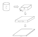
Fig. 2 is the figure of the method for explanation forge hot.
Fig. 3 utilizes opticmicroscope to take the photo of the silver alloys target of embodiment 1 with 30 times multiple.
Embodiment
Below, specifically describe the present invention based on embodiment.Should illustrate that as long as no especially explanation, and except the own situation of numerical value, % represents quality %.
(reflective electrode film of organic EL forms and uses the silver alloys target)
It is to have the In:0.1 of containing~1.5 quality % that the reflective electrode film of organic EL of the present invention forms with the large-scale target of silver alloys (hereinafter referred to as target of the present invention), the alloys target that becomes to be grouped into that remainder is made of Ag and inevitable impurity, it is characterized in that, the median size of the crystal grain of target of the present invention (hereinafter referred to as silver-indium alloy crystal grain) is 150~400 μ m, and the particle diameter deviation of above-mentioned silver-indium alloy crystal grain is below 20% of median size.
The target surface of target of the present invention (face for sputter one side of target) has 0.25m
2Above area for the situation of rectangular target, is more than the 500mm on one side at least, and from the angle consideration of the operability of target, the upper limit of length is preferably 2500mm.On the other hand, the angle of the upper limit of the size that used milling train generally can be rolling from cold rolling process considers that the upper limit of width is preferably 1700mm.In addition, consider that from the angle of the replacement frequency of target the thickness of target is preferably more than the 6mm, consider from the angle of the discharge stability of magnetron sputtering, be preferably below the 20mm.
Ag gives high-reflectivity and low resistance to the reflective electrode film of the organic EL that formed by sputter.
In improves the hardness of target, the warpage when therefore suppressing mechanical workout.Can suppress especially length is the above warpage of large-scale target when mechanical workout of 1m.And In has erosion resistance and the stable on heating effect of the reflective electrode film that improves the organic EL that is formed by sputter.This is because In has following effect: with the crystal grain miniaturization in the reflective electrode film, reduce the surfaceness of film, in addition, be solid-solubilized among the Ag and improve the intensity of crystal grain, the recrystallization that suppresses crystal grain suppresses the reduction of the reflectivity of the reflective electrode film that formed by sputter.The erosion resistance of reflective electrode film and stable on heating raising help high brightness, the long lifetime of organic EL.Further, owing to be that compositing range below the 21 quality % does not form the Compound Phase with Ag at In content, therefore when sputter, do not produce the paradoxical discharge that is caused by the different compound crystal grain of resistivity.
The content of In is less than 0.1 quality %, can not obtain the effect that the interpolation In of above-mentioned record brings.On the other hand, if the content of In surpasses 1.5 quality %, then show the characteristic of the low In of reflectivity, the reflectivity of the reflective electrode film that is formed by sputter reduces, so is not preferred.The forming of the reflective electrode film that is formed by sputter depend on target and form, the In content that therefore is contained in the silver alloys target is defined as In 0.1~1.5 quality %, more preferably 0.2~1.0 quality %.Wherein, the quantitative analysis of In is undertaken by inductively coupled plasma analytical method (ICP method).
The median size of the silver in the silver alloys target-indium alloy crystal grain is 150~400 μ m, preferred 200~350 μ m.When the median size of silver-indium alloy crystal grain than 150 μ m hours, it is large that crystallization particle diameter deviation becomes, and is easy to produce paradoxical discharge in the powerful sputter, splashes.On the other hand, when greater than 400 μ m, target is owing to sputter consumes, follow this, the difference of the sputter rate that is caused by the difference of the crystal orientation of each crystal grain causes that the concavo-convex change of sputtering surface is large, therefore is easy to the abnormal discharge in powerful sputter, produces easily and splashes.Wherein, the median size of silver-indium alloy crystal grain such as following mensuration.
In the sputter face of target, be rectangular parallelepiped sample about 10mm on one side from 16 station acquisition equably.Specifically, target is divided into 16 parts of vertical 4 * horizontal 4, from the central part collection sample of each several part.Should illustrate, in the present invention, the large-scale target that in forming organic EL, uses, has the sputter face more than 500 * 500(mm) of paying close attention to, therefore put down in writing by the method that gathers sample as the rectangular target of large-scale target normal operation, but the present invention also can bring into play effect certainly for the generation of splashing that suppresses circular.At this moment, according to the acquisition method of sample in the large-scale rectangular target, in the sputter face of target, be divided into equably 16 places, gather.
Sputter face side to each coupons is ground.After grinding with the waterproof paper of #180~#4000, polish with the abrasive material of 3 μ m~1 μ m.
Carry out etching, until available observation by light microscope is to the degree of grain boundary.Wherein, etching solution uses the mixed solution of aquae hydrogenii dioxidi and ammoniacal liquor, floods 1~2 second in room temperature, presents the grain boundary.Then, for each sample, be 30 times photo with optics microscope photographing multiple.
In each photo, draw in length and breadth the altogether line segment of 4 60mm with the interval of 20mm, form well word shape, number goes out the number of the crystal grain of each straight cuts.The crystal grain of line segment end is designated as 0.5.By L=60000/(M N) (wherein, M is actual multiple, and N is the mean value of number of die of cutting) try to achieve average slice length: L(μ m).
By the average slice length of trying to achieve: L(μ m), utilize d=(3/2) L calculates the median size of sample: d(μ m).
Will be from the mean value of the median size of the sample of the 16 station acquisition median size as the silver of target-indium alloy crystal grain.The median size of the silver of target of the present invention-indium alloy crystal grain is the scope of 150~400 μ m.
When the particle diameter deviation of silver-indium alloy crystal grain is 20% when following of median size of silver-indium alloy crystal grain, splashing in the time of can suppressing sputter more reliably.Wherein, with maximum that of the absolute value of the deviation of median size (| ((median size of certain 1 position)-(median size of position, 16 place)) |), use the median size (selection median size) of this selection as following, to calculate the particle diameter deviation in 16 median sizes that selection is tried to achieve by position, 16 place.| ((selection median size)-(median size of position, 16 place)) |/(median size of position, 16 place) * 100(%).
The silver alloys target is used in reflective electrode film formation according to organic EL of the present invention, even input is high-power in sputter, also can suppress paradoxical discharge, suppresses the generation of splashing.By this target is carried out sputter, can obtain the reflectivity height, have the reflective electrode film that organic EL of excellent durability uses.The present invention is that the above large-scale target of width: 500mm, length: 500mm, thickness 6mm is effective for target size especially.
The raw material that the reflective electrode film of (manufacture method) organic EL of the present invention forms with the silver alloys target has used purity: Ag and purity that 99.99 quality % are above: the In that 99.9 quality % are above.
At first, Ag is melted in high vacuum or atmosphere of inert gases, in the liquation that obtains, add the In of regulation content, then melt in vacuum or atmosphere of inert gases, making contains In:0.1~1.5 quality %, remainder is cast ingot casting by the melting of the Ag-In alloy that Ag and inevitable impurity consist of.Wherein, consider from the angle that the proportion of composing that makes Ag and In is stable that being melted in of preferred Ag makes atmosphere be first after the vacuum, carry out, adds In in the liquation of Ag after fusing in the argon atmosphere under the atmosphere with the argon displacement.
Then, for the median size that makes silver-indium alloy crystal grain is prescribed value, ingot casting is cast in melting carried out forge hot.Forge hot is preferably 750~850 ℃ of heating after 1~3 hour, repeats 6~20 forgings ratio and be 1/1.2~1/2 upsetting.Forge hot and then preferred open die forging, particularly preferably for example the limit makes the forging direction turn 90 ° of limits repetitions at every turn.In more detail, as shown in Figure 2, when using columned ingot casting, at first be forged into square.Then, make square ingot casting turn 90 ° from the forging direction of last time, repeat to forge.At this moment, be that the angle of prescribed value is considered from the median size of the silver that makes whole ingot casting-indium alloy crystal grain, more preferably be rotated, with square ingot casting vertically, laterally, all directions of short transverse (x of Fig. 2, y, z direction) forge.Wherein, the arrow of dotted line as shown in Figure 2 all represents to forge direction, and z represents casting direction, and x represents with respect to z to be 90 ° any direction, and y represents with respect to z and x to be 90 ° direction.For the median size of the silver that makes target of the present invention-indium alloy crystal grain is required numerical value, and the particle diameter deviation that makes silver-indium alloy crystal grain preferably repeats this operation in required scope.If multiplicity is less than 6 times, then above-mentioned effect is insufficient.On the other hand, even, suppressing the effect of the particle diameter deviation of silver-indium alloy crystal grain than more than 20 times, multiplicity do not have larger raising yet.In addition, the temperature of hot upset forging is during less than 750 ℃, owing to there is micro-crystallization, therefore can not give full play to particle diameter deviation inhibition, thus not preferred, if above 850 ℃, then owing to residual thick crystallization is arranged, so can not give full play to particle diameter deviation inhibition, thus not preferred.Should illustrate, in order to relax each rib of being formed by forge hot and/or the suddenly cooling in each bight, preferably under the degree of the forging that does not affect the ingot casting main body, suitably carry out this rib of forging ingot casting and/or the so-called chamfer angle in this bight.
Then, the ingot casting after forging is cold-rolled to required thickness, forms sheet material.Consider that from the angle of the inhibition of particle diameter deviation preferably this single pass draft in cold rolling is 5~10%.It is cold rolling to repeat this, (the ingot casting thickness before (the ingot casting thickness behind the ingot casting thickness before cold rolling-cold rolling)/cold rolling) is 60~75% until total reduction, this is prescribed value from making total reduction, and in the inhibition of keeping the particle diameter deviation, make the angle of crystallization particle diameter miniaturization consider it is preferred.In addition, in order to bring into play above-mentioned effect, preferred 10~20 passages.
Thermal treatment after cold rolling was carried out 1~2 hour at 550~650 ℃, and this angle from the median size that is controlled to regulation by recrystallization considers it is preferred.
By mill, the sheet material after with thermal treatment such as the mechanical workout of electrodischarge machining(E.D.M.) etc. is processed into required size, can make reflective electrode film and form and use the silver alloys target.The angle of splashing during from the inhibition sputter considers that the arithmetic mean surface roughness of the sputter face of the target after the mechanical workout (Ra) is preferably 0.2~2 μ m.
Embodiment
Below for the present invention, describe by embodiment, but the invention is not restricted to this.
(embodiment 1) (manufacturing of silver alloys target)
As raw material, preparing purity is that 99.99 quality % above Ag, purity are the above In of 99.9 quality %, in the high-frequency vacuum smelting furnace, is used as raw material with the filling Ag of the mass ratio shown in the table 1 and In.Total mass during fusing is about 300kg.
After carrying out vacuum exhaust in the vacuum chamber, with the displacement of Ar gas, after the Ag fusing, add In, alloy molten solution is cast in the graphite-made mold.Excision utilizes the shrinkage cavity part on the ingot casting top that casting makes, and as intact part, (φ 290 * 370mm) to obtain being about the ingot casting of 260kg.
The ingot casting that obtains 750~850 ℃ of heating after 1 hour, is repeated to make and forges direction and turn 90 ° at every turn, with respect to casting direction z, be 90 ° any direction x and be all directions of 90 ° direction y with respect to z and x with respect to z, forge.Making the single forging ratio is 1/1.2~1/2, changes direction, repeats 15 times upsetting.In the 16th time forging, extend, be configured as about 600 * 910 * 45(mm) size.
Ingot casting after forging is cold rolling, obtain about 1200 * 1300 * 16(mm) sheet material.Single pass draft in cold rolling is 5~10%, carries out altogether 15 passages.This cold rolling total reduction is 64%.
After rolling, sheet material was kept 1 hour 580 ℃ of heating, implement recrystallization and process.
Then this sheet material is machined into 1000 * 1200 * 12(mm) size, forms large-scale target of the present invention.
(evaluation of silver alloys target)
(1) warpage after the mechanical workout
The warpage of the silver alloys target after the mechanical workout of mensuration embodiment 1 the results are shown in table 2.
(2) particle size determination of the silver of target of the present invention-indium alloy crystal grain is as the mode that is used for carrying out an invention is put down in writing, from 1000 * 1200 * 12(mm) target of the present invention of above-mentioned manufacturing, equably by 16 place's station acquisition samples, mensuration is from the median size on the surface that the sputter face of each sample is observed, and calculates the deviation of the silver of the mean value of the median size of each sample-target of the present invention-median size of indium alloy crystal grain and the median size of silver-indium alloy crystal grain.Fig. 3 represents to utilize opticmicroscope with the photo of the silver alloys target of 30 times multiple shooting embodiment 1, the results are shown in table 1.For target of the present invention, the median size of silver-indium alloy crystal grain in the scope of 150~400 μ m, the particle diameter deviation of silver-indium alloy crystal grain be silver-indium alloy crystal grain median size 20% in.
(3) mensuration of the paradoxical discharge number of times during sputter
Cut out diameter from the arbitrary portion of 1000 * 1200 * 12(mm) target of the present invention of above-mentioned manufacturing: the plectane of 152.4mm, thickness: 6mm, and soldering is on the copper liner plate.This is welded the evaluation target that splashes when target is used as sputter, carries out the mensuration of paradoxical discharge number of times in the sputter.The results are shown in table 2.
The above-mentioned target that is welded is installed in common magnetic control sputtering device, is vented to 1 * 10
-4Behind the Pa, under the condition of distance: 60mm between Ar gaseous tension: 0.5Pa, power input: DC1000W, target substrate, carry out sputter.Paradoxical discharge number of times during sputter by MKS イ Application ス Star Le メ Application Star society DC power supply processed (model: electric arc tally function RPDG-50A), come instrumentation as 30 minutes paradoxical discharge number of times from discharge begins.The results are shown in table 2.For target of the present invention, the paradoxical discharge number of times is below 10 times.
(4) as the fundamental characteristics evaluation of organic EL film
(4-1) surfaceness of film
Use to be welded the silver alloys target shown in above-mentioned (3), with above-mentioned (2) same condition under carry out sputter, on 20 * 20(mm) glass substrate, with the thickness film forming of 100nm, obtain silver alloy film.Utilize atomic force microscope to measure the centre plane roughness (Ra) of this silver alloy film, the results are shown in table 2.Utilized the centre plane roughness Ra of film of target of the present invention for below the 1nm.
(4-2) reflectivity
Utilize the reflectivity of the silver alloy film of the same film forming of spectrophotometric determination and above-mentioned (4-1).Having utilized the absolute reflectance of silver alloy film under wavelength 550nm of target of the present invention is more than 90%.The results are shown in table 2.
(embodiment 2~4, comparative example 1~8)
Except the one-tenth for table 1 record was grouped into and creates conditions, other made target similarly to Example 1, obtain the silver alloys target of embodiment 2~4, comparative example 1~8 after, carry out similarly to Example 1 various evaluations.The results are shown in table 1 and table 2.
(conventional example 1,2)
Be grouped into similarly to Example 1 with the one-tenth of In of record in the table 1 and melt, graphite-made mold casting to square, make about 400 * 400 * 150(mm) ingot casting, further this ingot casting is carried out hot rolling 600 ℃ of heating after 1 hour, make the silver alloys target of conventional example 1.In addition, after will casting equally ingot casting and carry out hot rolling with conventional example 1, and then implement 600 ℃, 2 hours thermal treatment, make the silver alloys target of conventional example 2.Use the silver alloys target of conventional example 1 and conventional example 2, carry out equally various evaluations with the evaluation of embodiment 1.The results are shown in table 1 and table 2.
(reference example 1)
The proportioning of the In of record and charge weight is melted as 7kg in the table 1, alloy molten solution is cast in graphite casting die, make the ingot casting of φ 80 * 110(mm), the ingot casting that obtains is implemented upsetting number of times, cold rolling draft, the thermal treatment same with comparative example 3, obtain 220 * 220 * 11(mm) sheet material.Same with embodiment and comparative example, carry out various evaluations.The results are shown in table 1 and table 2.But the target of making in the target of reference example 1 and embodiment and the comparative example is compared, and size is little, does not therefore estimate the warpage after the mechanical workout.

As shown in Table 1, for embodiment 1~4, the median size of silver-indium alloy crystal grain is 160~360 μ m, and the particle diameter deviation is good, is 12~18%.Relative therewith, in the upsetting number of times was 5 times comparative example 3, the particle diameter deviation was large, is 25%, and in cold rolling total reduction was 40% comparative example 4, the particle diameter deviation was large, is 23%.In addition, in cold rolling total reduction was 80% comparative example 5, the particle diameter deviation was large, is 26%.Thermal treatment temp after cold rolling is 500 ℃ comparative example 6, the thermal treatment temp after cold rolling is that median size is respectively 92,460 μ m in 700 ℃ the comparative example 7 outside specialized range.Further, in the temperature of forge hot was 900 ℃ comparative example 8, median size was 440 μ m outside specialized range.In addition, the particle diameter deviation of conventional example 1 is large, is 120%, and conventional example 2 not only median size is large, be 550 μ m, and the particle diameter deviation is also large, is 35%.Reference example 1 be compare with the effective large-scale target of the present invention, the evaluation when making small-sized target, although with the same condition of comparative example 3 under make, the particle diameter deviation is good, is 17%.
As shown in Table 2, for embodiment 1~4, the absolute reflectance under the warpage after paradoxical discharge number of times, the mechanical workout, the surfaceness of film, the wavelength 550nm is good result.Relative therewith, be that the warpage after the mechanical workout is large in the comparative example 1 of 0.07 quality % at In, be 1.8mm, the surfaceness of film is also large, is 1.3 μ m.Being that the absolute reflectance under the wavelength 550nm is little in the comparative example 2 of 1.7 quality % at In, is 89.1%.In addition, for comparative example 3,4,6,7,8 and conventional example 1,2, paradoxical discharge is more than 13 times often.
As known from the above, reflective electrode film of the present invention forms can suppress paradoxical discharge with the silver alloys target, by with this target sputter, can improve reflectivity, and the surfaceness of reflectance coating is little, so can access the reflective electrode film that organic EL with excellent properties uses.
Should illustrate that technical scope of the present invention is not limited to above-mentioned embodiment and above-described embodiment, under the scope that does not break away from aim of the present invention, in addition various variations.
Claims (3)
1. the reflective electrode film of organic EL forms and uses the silver alloys target, it is characterized in that, have the In:0.1 of containing~1.5 quality %, remainder is become to be grouped into inevitable impurity consists of by Ag, the median size of the crystal grain of this alloy is 150~400 μ m, and the particle diameter deviation of above-mentioned crystal grain is below 20% of median size.
2. the reflective electrode film of organic EL claimed in claim 1 forms and uses the silver alloys target, it is characterized in that the target surface has 0.25m
2Above area.
3. the reflective electrode film of organic EL forms the manufacture method with the silver alloys target, it is characterized in that, carry out successively following operation: will have the In:0.1 of containing~1.5 quality %, remainder is repeated the operation of 6~20 hot upset forgings by Ag and the melting that becomes the to be grouped into casting ingot casting that inevitable impurity consists of, cold rolling operation, heat treated operation, the operation of mechanical workout, wherein the temperature of above-mentioned hot upset forging is 750~850 ℃, above-mentioned total reduction in cold rolling is 60~75%, above-mentioned heat treated temperature is 550~650 ℃, wherein the median size of the crystal grain of this alloy is 150~400 μ m, and the particle diameter deviation of above-mentioned crystal grain is below 20% of median size.
Applications Claiming Priority (5)
| Application Number | Priority Date | Filing Date | Title |
|---|---|---|---|
| JP2009232634 | 2009-10-06 | ||
| JP2009-232634 | 2009-10-06 | ||
| JP2010-210149 | 2010-09-17 | ||
| JP2010210149A JP4793502B2 (en) | 2009-10-06 | 2010-09-17 | Silver alloy target for forming reflective electrode film of organic EL element and method for producing the same |
| PCT/JP2010/067817 WO2011043486A1 (en) | 2009-10-06 | 2010-10-05 | Silver alloy target for forming reflection electrode film for organic el element, and method for manufacturing the silver alloy target |
Publications (2)
| Publication Number | Publication Date |
|---|---|
| CN102421931A CN102421931A (en) | 2012-04-18 |
| CN102421931B true CN102421931B (en) | 2013-10-30 |
Family
ID=43856934
Family Applications (1)
| Application Number | Title | Priority Date | Filing Date |
|---|---|---|---|
| CN2010800200309A Active CN102421931B (en) | 2009-10-06 | 2010-10-05 | Silver alloy target for forming reflection electrode film for organic EL element, and method for manufacturing silver alloy target |
Country Status (7)
| Country | Link |
|---|---|
| US (1) | US8821769B2 (en) |
| EP (1) | EP2487274B1 (en) |
| JP (1) | JP4793502B2 (en) |
| KR (1) | KR101099415B1 (en) |
| CN (1) | CN102421931B (en) |
| TW (1) | TWI385263B (en) |
| WO (1) | WO2011043486A1 (en) |
Families Citing this family (16)
| Publication number | Priority date | Publication date | Assignee | Title |
|---|---|---|---|---|
| JP5533545B2 (en) * | 2010-01-12 | 2014-06-25 | 三菱マテリアル株式会社 | Silver alloy target for forming reflective electrode film of organic EL element and method for producing the same |
| JP5806653B2 (en) * | 2011-12-27 | 2015-11-10 | 株式会社神戸製鋼所 | Ag alloy film for reflective electrode, reflective electrode, and Ag alloy sputtering target |
| JP5159962B1 (en) * | 2012-01-10 | 2013-03-13 | 三菱マテリアル株式会社 | Silver alloy sputtering target for forming conductive film and method for producing the same |
| JP5472353B2 (en) | 2012-03-27 | 2014-04-16 | 三菱マテリアル株式会社 | Silver-based cylindrical target and manufacturing method thereof |
| DE102012006718B3 (en) * | 2012-04-04 | 2013-07-18 | Heraeus Materials Technology Gmbh & Co. Kg | Planar or tubular sputtering target and method of making the same |
| JP5928218B2 (en) * | 2012-07-20 | 2016-06-01 | 三菱マテリアル株式会社 | Ag alloy film and manufacturing method thereof |
| JP2014196562A (en) * | 2012-12-21 | 2014-10-16 | 三菱マテリアル株式会社 | Ag alloy sputtering target |
| JP5522599B1 (en) * | 2012-12-21 | 2014-06-18 | 三菱マテリアル株式会社 | Ag alloy sputtering target |
| JP5612147B2 (en) * | 2013-03-11 | 2014-10-22 | 三菱マテリアル株式会社 | Silver alloy sputtering target for forming conductive film and method for producing the same |
| JP6198177B2 (en) * | 2013-07-19 | 2017-09-20 | 三菱マテリアル株式会社 | Ag alloy sputtering target |
| CN105316630B (en) * | 2014-06-04 | 2020-06-19 | 光洋应用材料科技股份有限公司 | Silver alloy target material, manufacturing method thereof and organic light-emitting diode applying same |
| DE102014214683A1 (en) | 2014-07-25 | 2016-01-28 | Heraeus Deutschland GmbH & Co. KG | Sputtering target based on a silver alloy |
| EP3168325B1 (en) | 2015-11-10 | 2022-01-05 | Materion Advanced Materials Germany GmbH | Silver alloy based sputter target |
| CN106893989B (en) * | 2016-12-29 | 2019-10-01 | 昆山全亚冠环保科技有限公司 | A kind of silver titanium alloy target crack resistence rolling mill practice |
| JP2019143242A (en) | 2018-02-20 | 2019-08-29 | 三菱マテリアル株式会社 | Ag ALLOY SPUTTERING TARGET AND MANUFACTURING METHOD OF Ag ALLOY SPUTTERING TARGET |
| WO2019163745A1 (en) * | 2018-02-20 | 2019-08-29 | 三菱マテリアル株式会社 | Ag alloy sputtering target and method for manufacturing ag alloy sputtering target |
Citations (3)
| Publication number | Priority date | Publication date | Assignee | Title |
|---|---|---|---|---|
| US5456815A (en) * | 1993-04-08 | 1995-10-10 | Japan Energy Corporation | Sputtering targets of high-purity aluminum or alloy thereof |
| WO2003100112A1 (en) * | 2002-05-28 | 2003-12-04 | Ishifuku Metal Industry Co., Ltd. | Sputtering target material |
| CN1823179A (en) * | 2003-07-16 | 2006-08-23 | 株式会社神户制钢所 | Ag base sputtering target and process for producing the same |
Family Cites Families (4)
| Publication number | Priority date | Publication date | Assignee | Title |
|---|---|---|---|---|
| JP3856386B2 (en) | 2001-03-16 | 2006-12-13 | 石福金属興業株式会社 | Sputtering target material |
| JP4264302B2 (en) * | 2002-06-24 | 2009-05-13 | 株式会社コベルコ科研 | Silver alloy sputtering target and manufacturing method thereof |
| CN1238554C (en) * | 2002-06-24 | 2006-01-25 | 株式会社钢臂功科研 | Silver alloy sputtering target and its producing method |
| JP4351144B2 (en) * | 2004-12-08 | 2009-10-28 | 田中貴金属工業株式会社 | Silver alloy |
-
2010
- 2010-09-17 JP JP2010210149A patent/JP4793502B2/en active Active
- 2010-10-05 WO PCT/JP2010/067817 patent/WO2011043486A1/en active Application Filing
- 2010-10-05 US US13/500,224 patent/US8821769B2/en active Active
- 2010-10-05 EP EP10822155.7A patent/EP2487274B1/en active Active
- 2010-10-05 KR KR1020117022697A patent/KR101099415B1/en active IP Right Grant
- 2010-10-05 CN CN2010800200309A patent/CN102421931B/en active Active
- 2010-10-06 TW TW099134036A patent/TWI385263B/en active
Patent Citations (3)
| Publication number | Priority date | Publication date | Assignee | Title |
|---|---|---|---|---|
| US5456815A (en) * | 1993-04-08 | 1995-10-10 | Japan Energy Corporation | Sputtering targets of high-purity aluminum or alloy thereof |
| WO2003100112A1 (en) * | 2002-05-28 | 2003-12-04 | Ishifuku Metal Industry Co., Ltd. | Sputtering target material |
| CN1823179A (en) * | 2003-07-16 | 2006-08-23 | 株式会社神户制钢所 | Ag base sputtering target and process for producing the same |
Also Published As
| Publication number | Publication date |
|---|---|
| TWI385263B (en) | 2013-02-11 |
| EP2487274A1 (en) | 2012-08-15 |
| JP4793502B2 (en) | 2011-10-12 |
| US8821769B2 (en) | 2014-09-02 |
| CN102421931A (en) | 2012-04-18 |
| KR101099415B1 (en) | 2011-12-27 |
| TW201131001A (en) | 2011-09-16 |
| EP2487274B1 (en) | 2018-09-26 |
| US20120193589A1 (en) | 2012-08-02 |
| JP2011100719A (en) | 2011-05-19 |
| WO2011043486A1 (en) | 2011-04-14 |
| EP2487274A4 (en) | 2017-05-24 |
| KR20110113214A (en) | 2011-10-14 |
Similar Documents
| Publication | Publication Date | Title |
|---|---|---|
| CN102421931B (en) | Silver alloy target for forming reflection electrode film for organic EL element, and method for manufacturing silver alloy target | |
| CN103443323B (en) | Silver alloy sputtering target for forming electroconductive film, and method for manufacture same | |
| TWI576442B (en) | Ag alloy sputtering target for forming conductive film and method of manufacturing the same | |
| CN103298970B (en) | Silver-alloy sputtering target for conductive-film formation, and method for producing same | |
| JP5533545B2 (en) | Silver alloy target for forming reflective electrode film of organic EL element and method for producing the same | |
| CN105378140B (en) | Ag alloy sputtering targets | |
| CN103958727B (en) | Conductive film formation silver alloy sputtering target and manufacture method thereof | |
| JP5830907B2 (en) | Silver alloy sputtering target for forming conductive film and method for producing the same | |
| JP5830908B2 (en) | Silver alloy sputtering target for forming conductive film and method for producing the same | |
| JP5669014B2 (en) | Silver alloy sputtering target for forming conductive film and method for producing the same | |
| JP6375829B2 (en) | Ag alloy sputtering target | |
| JP5669015B2 (en) | Silver alloy sputtering target for forming conductive film and method for producing the same | |
| CN102041479B (en) | Al-based alloy sputtering target |
Legal Events
| Date | Code | Title | Description |
|---|---|---|---|
| C06 | Publication | ||
| PB01 | Publication | ||
| C10 | Entry into substantive examination | ||
| SE01 | Entry into force of request for substantive examination | ||
| C14 | Grant of patent or utility model | ||
| GR01 | Patent grant |