CN102307282A - 具有扩展的动态范围的图像传感器 - Google Patents
具有扩展的动态范围的图像传感器 Download PDFInfo
- Publication number
- CN102307282A CN102307282A CN201110283424XA CN201110283424A CN102307282A CN 102307282 A CN102307282 A CN 102307282A CN 201110283424X A CN201110283424X A CN 201110283424XA CN 201110283424 A CN201110283424 A CN 201110283424A CN 102307282 A CN102307282 A CN 102307282A
- Authority
- CN
- China
- Prior art keywords
- pixel
- integration
- time
- pixels
- pattern
- Prior art date
- Legal status (The legal status is an assumption and is not a legal conclusion. Google has not performed a legal analysis and makes no representation as to the accuracy of the status listed.)
- Pending
Links
Images


Classifications
-
- H—ELECTRICITY
- H04—ELECTRIC COMMUNICATION TECHNIQUE
- H04N—PICTORIAL COMMUNICATION, e.g. TELEVISION
- H04N25/00—Circuitry of solid-state image sensors [SSIS]; Control thereof
- H04N25/50—Control of the SSIS exposure
- H04N25/57—Control of the dynamic range
- H04N25/58—Control of the dynamic range involving two or more exposures
- H04N25/581—Control of the dynamic range involving two or more exposures acquired simultaneously
- H04N25/583—Control of the dynamic range involving two or more exposures acquired simultaneously with different integration times
-
- H—ELECTRICITY
- H04—ELECTRIC COMMUNICATION TECHNIQUE
- H04N—PICTORIAL COMMUNICATION, e.g. TELEVISION
- H04N25/00—Circuitry of solid-state image sensors [SSIS]; Control thereof
- H04N25/50—Control of the SSIS exposure
- H04N25/57—Control of the dynamic range
-
- H—ELECTRICITY
- H04—ELECTRIC COMMUNICATION TECHNIQUE
- H04N—PICTORIAL COMMUNICATION, e.g. TELEVISION
- H04N23/00—Cameras or camera modules comprising electronic image sensors; Control thereof
- H04N23/10—Cameras or camera modules comprising electronic image sensors; Control thereof for generating image signals from different wavelengths
-
- H—ELECTRICITY
- H04—ELECTRIC COMMUNICATION TECHNIQUE
- H04N—PICTORIAL COMMUNICATION, e.g. TELEVISION
- H04N23/00—Cameras or camera modules comprising electronic image sensors; Control thereof
- H04N23/80—Camera processing pipelines; Components thereof
- H04N23/84—Camera processing pipelines; Components thereof for processing colour signals
-
- H—ELECTRICITY
- H04—ELECTRIC COMMUNICATION TECHNIQUE
- H04N—PICTORIAL COMMUNICATION, e.g. TELEVISION
- H04N25/00—Circuitry of solid-state image sensors [SSIS]; Control thereof
-
- H—ELECTRICITY
- H04—ELECTRIC COMMUNICATION TECHNIQUE
- H04N—PICTORIAL COMMUNICATION, e.g. TELEVISION
- H04N25/00—Circuitry of solid-state image sensors [SSIS]; Control thereof
- H04N25/10—Circuitry of solid-state image sensors [SSIS]; Control thereof for transforming different wavelengths into image signals
- H04N25/11—Arrangement of colour filter arrays [CFA]; Filter mosaics
- H04N25/13—Arrangement of colour filter arrays [CFA]; Filter mosaics characterised by the spectral characteristics of the filter elements
- H04N25/134—Arrangement of colour filter arrays [CFA]; Filter mosaics characterised by the spectral characteristics of the filter elements based on three different wavelength filter elements
Abstract
图像传感器包括:多个像素;跨越像素的至少一部分的滤色器图案,其中,滤色器图案形成具有按照预定排列的色彩的滤色器核心;以及用于控制像素的积分时间的装置,其中,多个像素的积分时间在与滤色器阵列核心相关的图案中在空间上变化。
Description
本申请是国际申请日为2004年9月1日、申请号为“200480024674.X”且发明名称为“具有扩展的动态范围的图像传感器”的专利申请的分案申请。
发明领域
本发明涉及具有增加的动态范围、基于半导体的图像传感器。
发明背景
固态图像传感器现在广泛地用于许多类型的图像捕捉应用。所采用的两种主要图像传感器技术是电荷耦合器件CCD和CMOS x-y可寻址器件。目前存在这两种技术的许多不同的具体实施例,其中包括有源像素传感器(APS)以及CMOS x-y可寻址器件的无源像素传感器(PPS)。基本上全部由光电检测器组或阵列构成,它们把入射光转换为可被读出并且用来构造与入射光图案相关的图像的电信号。光电检测器阵列的曝光或积分时间可由众所周知的装置来控制。信号表示入射到像素感光单元上的光的量。成像感应器件的动态范围(DR)被定义为通常称作饱和信号(Vsat)的有效最大可检测信号电平与传感器的rms.噪声电平(σ噪声)之比。这如等式1所示。
等式1:动态范围=Vsat/σ噪声。
图像传感器器件、例如对入射光子建立的电荷积分的电荷耦合器件(CCD)的动态范围由给定感光单元中可收集并保持的电荷量(Vsat)来限制。例如,对于任何给定的CCD,在一个像素中可收集并检测的电荷量与像素面积成比例。因此,对于百万像素数字照相机(DSC)中使用的商用器件,表示Vsat的电子数量大约为13000到20000个电子。如果入射光极亮并且建立可在像素或光电检测器中保持的更多电子,则这些过剩电子由像素中的消除模糊装置提取,并且不构成增加的饱和信号。因此,最大可检测信号电平被限制到光电检测器或像素中可保持的电荷量。DR也由传感器噪声电平σ噪声来限制。由于对Vsat的限制,在CCD中进行许多工作将σ噪声降到极低水平。商用百万像素DSC器件具有1000:1或以下的DR。
DR上的相同限制对于APS和PPS器件也存在。Vsat由光电检测器中可保持并隔离的电荷量来限制。过剩电荷丢失。与CCD相比,由于像素中限制可用于光电检测器的面积的有源和无源元件,以及由于CMOS器件中采用的低电压电源和时钟,这对于APS和PPS更成问题。另外,由于APS器件已经用来提供芯片上的图像传感器系统,因此,CCD上没有的、在APS器件上采用的数字和模拟电路、例如定时和控制及模数转换与CCD相比在APS器件上提供高得多的固有噪声电平。这是由于较高的瞬时噪声以及来自芯片上的模数转换器的可能的量化噪声。
在共同转让的美国专利6069377中,Guidash公开了扩展APS器件的动态范围的先有技术方法,并且公开了扩展动态范围的一种新发明。这种方法的缺点是每个像素需要四个以上晶体管,并且限制了可制作的像素的尺寸。在美国专利6307195和6486504中,Guidash公开了通过收集从光电检测器大量出现的电荷以及通过把光电检测器和浮动扩散共同集成在单个像素中来扩展动态范围。这些方法可能的缺点是构成传感器中的固定图案噪声的光电检测器饱和电平的空间变化,并且不增加传感器的灵敏度。
先有技术的APS器件还因像素中有源元件的集成以及入射光通过设置在像素上的滤色器层的传输损失导致的有限填充因数而具有对光的很差灵敏度。
从以上论述中应当清楚,先有技术中仍然需要保持扩展的动态范围、同时保持低固定图案噪声、小像素和高灵敏度的器件。
发明内容
本发明提供一种分别对图像传感器上的任何给定空间图案、更具体是对与CFA图案中的核心的一维或二维兼容的图案控制积分的装置。这通过为给定行或行集合中的像素提供分开的TG或RG总线,或者通过提供分别对图像传感器阵列中的像素的给定图案控制积分时间的任何装置来进行。这样,有效数据始终可同时用于图像的暗和亮区域。
本发明的有利效果
通过阅读以下优选实施例的详细说明和所附权利要求并参照附图,会更清晰地理解和认识本发明的这些和其它方面、目的、特征及优点。
附图简介
图1a是先有技术的像素阵列;
图1b是另一个先有技术的像素阵列;
图2a是本发明的一个像素阵列;
图2b是本发明的一个备选实施例;
图3是图表,以图形方式说明图2a和图2b的实现;
图4a是每行两个积分控制线的图示;
图4b是每行一个积分时间信号线的图示;
图5是用于把图2a和图2b的像素阵列实现为优选商用实施例的照相机。
发明详细说明
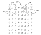
典型的先有技术图像传感器像素阵列如图1a和图1b所示。图1a中的图像传感器可能属于任何技术类型、如CCD或CMOS APS。图1a中的像素阵列10包括一组光电检测器。积分时间对于各像素是恒定的,由全部具有相同积分时间的区域10a中的像素代表。这种方法的缺点在于,如果积分时间长,则图像的亮区中的像素将变为饱和,以及亮区域中的图像细节将丢失。如果积分时间被选择为较短,则图像的暗区域中的图像质量因低信号和高噪声而会很差。在Guidash于2002年7月17日提交的标题为“具有可编程色彩平衡的有源像素传感器”的美国专利申请序号08/960418中公开了图1b中的图像传感器,在其中,与CFA图案关联的像素阵列20的各色彩具有各自的积分时间,以便取得电荷域白平衡。这在图1b中由表示为20a的区域即绿-红行中的绿像素、区域20b即绿-红行中的红像素、区域20c即绿-蓝行中的蓝像素以及区域20d即绿-蓝行中的绿像素来表示。这具有与对于图1a中的图像传感器像素阵列所述的相同缺点。
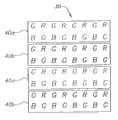
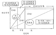
参照图2a,本发明的图像传感器像素阵列30包括有助于不同的可编程积分时间、但按照与图1b所示不同的空间图案的阵列。对于x-y可寻址CMOS图像传感器,这可采用分开的传输门或复位门来实现。对于CCD图像传感器,这可通过包含分开的传输门来实现。图2a中的图像传感器像素阵列30构造成包括对于与滤色器阵列图案节距或核心相关的成对的行40a和40b具有两个不同积分时间的像素。具有长积分时间的像素称作快像素。具有短积分时间的像素称作慢像素。在Bayer CFA图案的情况中,这是两行节距。通过在这个图案中具有分开的积分时间,图像传感器的有效动态范围如图3所示被扩展。在区域1、即低亮度级区域中,传感器的慢和快两种像素没有饱和。快像素将具有远高于固有噪声电平的信号电平。慢像素将具有与传感器固有噪声电平相比在预定比率内的信号电平。在区域2中,慢和快两种像素都没有饱和,并且两者都具有足够的信噪比。在区域3、即高亮度级区域中,快像素已经饱和或者被削减,并且没有包含有效信号电平信息。慢像素没有饱和,并且包含具有足够信噪比的有效信号电平信息。由于有效信息与CFA图案相关,因此,来自快像素的丢失信息可通过慢像素的内插来确定。对于图3所示的分开积分时间体系结构,采取单帧捕捉,并且执行空间自适应图像处理。在区域2中,标准的先有技术彩色图像处理方法用来呈现图像。对于属于区域3中的图像捕捉中的像素面积,慢像素的内插用来确定快像素中的丢失信号信息。这导致图像的极亮面积中的真实MTF的损失,但是产生有效的更高饱和照度Isat。这有效地扩展图像传感器的画面内动态范围。虽然真实空间分辨率在极亮区域中下降,但是,在图像捕捉中原本会丢失的图像内容被保存。
图2a的传感器体系结构设计成为积分时间图案提供第一积分时间的两行,以及具有第二积分时间的两个相邻行。这可采用任何类型的图像传感器、通过在这个图案中具有积分时间的多个或分开的控制来实现。对于CMOS和其它x-y可寻址图像传感器,这可只是通过让图像传感器定时采用应用于控制积分时间的交替行信号线对的独立的两组积分指针来安排来实现。这可能是各行中的传输门线或各行中的复位门线或者用来控制那一行的积分时间的其它任何每行信号。在CCD图像传感器的情况中,这要求构造传输门互连,使得至少对于行的交替对存在到传输门线的独立和分隔的连接。
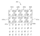
本发明的第二实施例以图2b中的阵列来表示。在这个实施例中,传感器阵列50构造成在2×2像素图案60a和60b中具有两个分开且可编程的积分时间。在x-y可寻址图像传感器技术的情况中,这通过每行包括多个信号线来实现,它们用来控制积分时间,例如传输门或复位门。每行的多个信号线连接到像素的交替对,以便产生图2b所示的积分时间图案。
参照图4a,说明控制积分时间的多个信号线70的路由选择。采用路由多个信号线70来控制各行的积分时间的一个缺点是填充因数减小或者更大的像素尺寸,以便使额外的信号线适合像素节距。这通过图4b所示的信号线路由选择体系结构来解决。在这种情况中,每行使用单个积分时间控制线80,但它实际上被路由到两个相邻行中的像素。相邻行中的信号线80以类似于创建图2b所示的积分时间图案的方式被路由。通过这种方法,虽然一次从传感器读出单行数据,但数据流中包含的像素是来自阵列中的物理上相邻的行。为了正确地重构图像,隔行数据必须在照相机图像存储器中进行校正。这也是本发明的一个特征。由于芯片上或照相机内的存储器可设置成把数据写入两行或两行以上的位置,因此不需要让传感器同时从物理行中读出所有像素。
如上所述,这为图像传感器和图像捕捉系统提供了画面内动态范围和宽曝光宽容度。单一图像捕捉可呈现具有对于低亮度级的积分时间的优化的全范围的图像信息,而没有削减图像的高亮度区域中的信号信息。这可极大地简化成像系统中的曝光控制系统和算法,因为曝光或积分时间的选择不需要非常精确。
还应当注意,采用这种传感器的图像捕捉系统可用来测量或确定画面的动态范围,以便适当设置两个积分时间。在照相机系统的计量阶段,两个分开很宽的积分时间可用来确定画面中的最大和最小亮度级。两个积分时间则可调整为覆盖画面中的照明范围。例如,如果要捕捉的画面的动态范围处于图像传感器的固有动态范围之内,则两个积分时间可设置为相同的值。如果画面包含比传感器的真实动态范围更宽的动态范围,则两个积分时间可设置为匹配或最佳地覆盖画面的动态范围。
参照图5,说明用于实现本发明的图像传感器的照相机90,它是许多面向消费者的商业实施例之一。
参照一个优选实施例描述了本发明。但是,大家会理解,本领域的技术人员可进行各种变更和修改,而没有背离本发明的范围。
配件表
10 像素阵列
20 像素阵列
20a 绿像素,在绿-红行中
20b 红像素,在绿-红行中
20c 蓝像素,在绿-蓝行中
20d 绿像素,在绿-蓝行中
30 像素阵列
40a 成对的行
40b 成对的行
50 传感器阵列
60a 2×2像素图案
60b 2×2像素图案
70 多个信号线
80 单积分时间控制线
90 照相机
Claims (3)
1.一种具有增加的动态范围、基于半导体的图像传感器,包括:
(a) 多个像素;
(b) 跨越所述像素的至少一部分的滤色器图案,其中,所述滤色器图案包括各具有多个像素和相应的滤色器图案的多个滤色器核心;以及
(c) 用于控制所述像素的积分时间的装置,其中,所述多个像素的积分时间在与滤色器核心相关的图案中在空间上变化,
其中,所述多个像素的积分时间图案包括具有第一积分时间的第一两行像素以及具有第二积分时间的相邻的第二两行像素。
2.一种照相机,包括:
(a) 具有增加的动态范围、基于半导体的图像传感器,所述图像传感器包括:
(a1) 多个像素;
(a2) 跨越所述像素的至少一部分的滤色器图案,其中,所述滤色器图案包括各具有多个像素和相应的滤色器图案的多个滤色器核心;以及
(a3) 用于控制所述像素的积分时间的装置,其中,所述多个像素的积分时间在与滤色器核心相关的图案中在空间上变化,
其中,所述多个像素的积分时间图案包括具有第一积分时间的第一两行像素以及具有第二积分时间的相邻的第二两行像素。
3.如权利要求2所述的照相机,其特征在于,还包括至少读出所述多个像素的子集并且采用从所述读出得到的信号值来确定所述多个像素的积分时间的装置。
Applications Claiming Priority (2)
| Application Number | Priority Date | Filing Date | Title |
|---|---|---|---|
| US10/654313 | 2003-09-03 | ||
| US10/654,313 US7830435B2 (en) | 2003-09-03 | 2003-09-03 | Image sensor and image capture system with extended dynamic range |
Related Parent Applications (1)
| Application Number | Title | Priority Date | Filing Date |
|---|---|---|---|
| CN200480024674XA Division CN1843027B (zh) | 2003-09-03 | 2004-09-01 | 具有扩展的动态范围的图像传感器 |
Publications (1)
| Publication Number | Publication Date |
|---|---|
| CN102307282A true CN102307282A (zh) | 2012-01-04 |
Family
ID=34218061
Family Applications (2)
| Application Number | Title | Priority Date | Filing Date |
|---|---|---|---|
| CN201110283424XA Pending CN102307282A (zh) | 2003-09-03 | 2004-09-01 | 具有扩展的动态范围的图像传感器 |
| CN200480024674XA Active CN1843027B (zh) | 2003-09-03 | 2004-09-01 | 具有扩展的动态范围的图像传感器 |
Family Applications After (1)
| Application Number | Title | Priority Date | Filing Date |
|---|---|---|---|
| CN200480024674XA Active CN1843027B (zh) | 2003-09-03 | 2004-09-01 | 具有扩展的动态范围的图像传感器 |
Country Status (7)
| Country | Link |
|---|---|
| US (2) | US7830435B2 (zh) |
| EP (1) | EP1661390A2 (zh) |
| JP (1) | JP2007504770A (zh) |
| KR (1) | KR101038386B1 (zh) |
| CN (2) | CN102307282A (zh) |
| TW (1) | TWI387334B (zh) |
| WO (1) | WO2005024948A2 (zh) |
Cited By (1)
| Publication number | Priority date | Publication date | Assignee | Title |
|---|---|---|---|---|
| CN109417603A (zh) * | 2016-04-26 | 2019-03-01 | 新成像技术公司 | 具有两个传感器的成像器系统 |
Families Citing this family (45)
| Publication number | Priority date | Publication date | Assignee | Title |
|---|---|---|---|---|
| US7489352B2 (en) * | 2002-11-15 | 2009-02-10 | Micron Technology, Inc. | Wide dynamic range pinned photodiode active pixel sensor (APS) |
| FR2861242B1 (fr) * | 2003-10-17 | 2006-01-20 | Trixell Sas | Procede de commande d'un dispositif photosensible |
| US7446812B2 (en) * | 2004-01-13 | 2008-11-04 | Micron Technology, Inc. | Wide dynamic range operations for imaging |
| US8081234B2 (en) * | 2004-12-29 | 2011-12-20 | Intel Corporation | Technique for increased exposure range in image sensors |
| US7214998B2 (en) * | 2005-07-26 | 2007-05-08 | United Microelectronics Corp. | Complementary metal oxide semiconductor image sensor layout structure |
| KR100769548B1 (ko) | 2005-12-30 | 2007-10-23 | 엠텍비젼 주식회사 | 컬러 필터 어레이 및 영상 보간 방법 |
| JP4487944B2 (ja) * | 2006-02-09 | 2010-06-23 | ソニー株式会社 | 固体撮像装置 |
| US20080198251A1 (en) * | 2007-02-15 | 2008-08-21 | Micron Technology, Inc. | Method, apparatus, and system providing multiple pixel integration periods |
| US20100044676A1 (en) | 2008-04-18 | 2010-02-25 | Invisage Technologies, Inc. | Photodetectors and Photovoltaics Based on Semiconductor Nanocrystals |
| US7923801B2 (en) | 2007-04-18 | 2011-04-12 | Invisage Technologies, Inc. | Materials, systems and methods for optoelectronic devices |
| KR101380615B1 (ko) * | 2007-06-28 | 2014-04-14 | 삼성전자주식회사 | 영상 동적 범위 향상 방법 및 장치 |
| JP4480740B2 (ja) * | 2007-07-03 | 2010-06-16 | シャープ株式会社 | 固体撮像素子およびその製造方法、電子情報機器 |
| KR101424717B1 (ko) * | 2007-09-13 | 2014-08-01 | 삼성전자주식회사 | 노출 시간 설정 장치 및 방법 |
| US8102435B2 (en) | 2007-09-18 | 2012-01-24 | Stmicroelectronics S.R.L. | Method for acquiring a digital image with a large dynamic range with a sensor of lesser dynamic range |
| US7940311B2 (en) * | 2007-10-03 | 2011-05-10 | Nokia Corporation | Multi-exposure pattern for enhancing dynamic range of images |
| US8203195B2 (en) | 2008-04-18 | 2012-06-19 | Invisage Technologies, Inc. | Materials, fabrication equipment, and methods for stable, sensitive photodetectors and image sensors made therefrom |
| US8405750B2 (en) * | 2009-06-08 | 2013-03-26 | Aptina Imaging Corporation | Image sensors and image reconstruction methods for capturing high dynamic range images |
| US8605177B2 (en) * | 2009-09-16 | 2013-12-10 | Altasens, Inc. | Image sensor with wide dynamic range |
| US8134628B2 (en) * | 2009-09-30 | 2012-03-13 | Truesense Imaging, Inc. | Methods for capturing and reading out images from an image sensor |
| US8279317B2 (en) * | 2009-09-30 | 2012-10-02 | Truesense Imaging, Inc. | Methods for capturing and reading out images from an image sensor |
| US8194164B2 (en) * | 2009-09-30 | 2012-06-05 | Truesense Imaging, Inc. | Methods for capturing and reading out images from an image sensor |
| US8194166B2 (en) | 2009-09-30 | 2012-06-05 | Truesense Imaging, Inc. | Methods for capturing and reading out images from an image sensor |
| US20110074997A1 (en) * | 2009-09-30 | 2011-03-31 | Border John N | Methods for capturing and reading out images from an image sensor |
| US8194165B2 (en) | 2009-09-30 | 2012-06-05 | Truesense Imaging, Inc. | Methods for capturing and reading out images from an image sensor |
| US8314873B2 (en) | 2009-09-30 | 2012-11-20 | Truesense Imaging, Inc. | Methods for capturing and reading out images from an image sensor |
| US8144220B2 (en) | 2009-09-30 | 2012-03-27 | Truesense Imaging, Inc. | Methods for capturing and reading out images from an image sensor |
| US8279316B2 (en) * | 2009-09-30 | 2012-10-02 | Truesense Imaging, Inc. | Methods for capturing and reading out images from an image sensor |
| US8294803B2 (en) * | 2009-09-30 | 2012-10-23 | Truesense Imaging, Inc. | Methods for capturing and reading out images from an image sensor |
| US8149303B2 (en) * | 2009-09-30 | 2012-04-03 | Truesense Imaging, Inc. | Methods for capturing and reading out images from an image sensor |
| US8916947B2 (en) | 2010-06-08 | 2014-12-23 | Invisage Technologies, Inc. | Photodetector comprising a pinned photodiode that is formed by an optically sensitive layer and a silicon diode |
| US8890986B2 (en) * | 2011-04-27 | 2014-11-18 | Aptina Imaging Corporation | Method and apparatus for capturing high dynamic range images using multi-frame interlaced exposure images |
| JP2012257193A (ja) | 2011-05-13 | 2012-12-27 | Sony Corp | 画像処理装置、撮像装置、および画像処理方法、並びにプログラム |
| US8913153B2 (en) * | 2011-10-06 | 2014-12-16 | Aptina Imaging Corporation | Imaging systems and methods for generating motion-compensated high-dynamic-range images |
| US8576979B2 (en) * | 2011-10-11 | 2013-11-05 | Omnivision Technologies, Inc. | Arithmetic counter circuit, configuration and application for high performance CMOS image sensors |
| US20130128083A1 (en) * | 2011-11-23 | 2013-05-23 | Himax Imaging Limited | High dynamic range image sensing device and image sensing method and manufacturing method thereof |
| US9172889B2 (en) | 2012-02-09 | 2015-10-27 | Semiconductor Components Industries, Llc | Imaging systems and methods for generating auto-exposed high-dynamic-range images |
| US9007488B2 (en) | 2012-03-08 | 2015-04-14 | Semiconductor Components Industries, Llc | Systems and methods for generating interpolated high-dynamic-range images |
| US9338372B2 (en) | 2012-09-19 | 2016-05-10 | Semiconductor Components Industries, Llc | Column-based high dynamic range imaging systems |
| JP2014086889A (ja) * | 2012-10-24 | 2014-05-12 | Toshiba Corp | 固体撮像装置 |
| CN103139491A (zh) * | 2013-03-25 | 2013-06-05 | 天利半导体(深圳)有限公司 | 一种高动态范围低噪声的cmos 传感器芯片 |
| US9941316B2 (en) | 2014-06-10 | 2018-04-10 | Invisage Technologies, Inc. | Multi-terminal optoelectronic devices for light detection |
| KR20160071203A (ko) | 2014-12-11 | 2016-06-21 | 삼성전자주식회사 | 이미지 신호 프로세서, 이의 작동 방법, 및 이를 포함하는 모바일 컴퓨팅 장치 |
| US11050945B2 (en) | 2018-07-06 | 2021-06-29 | Samsung Electronics Co., Ltd. | Method and apparatus for capturing dynamic images |
| CN110531401B (zh) * | 2019-09-11 | 2021-04-09 | 南华大学 | 核辐射探测器及核辐射探测方法 |
| KR20220101694A (ko) | 2019-11-20 | 2022-07-19 | 기가조트 테크널러지 인코포레이티드 | 스케일러블 픽셀 크기 이미지센서 |
Citations (2)
| Publication number | Priority date | Publication date | Assignee | Title |
|---|---|---|---|---|
| EP1227661A2 (en) * | 2001-01-24 | 2002-07-31 | Eastman Kodak Company | Method and apparatus for generating and storing extended dynamic range digital images |
| US6665010B1 (en) * | 1998-07-21 | 2003-12-16 | Intel Corporation | Controlling integration times of pixel sensors |
Family Cites Families (20)
| Publication number | Priority date | Publication date | Assignee | Title |
|---|---|---|---|---|
| US3971065A (en) * | 1975-03-05 | 1976-07-20 | Eastman Kodak Company | Color imaging array |
| EP0565295B1 (en) * | 1992-04-10 | 1997-11-26 | Mitsubishi Denki Kabushiki Kaisha | Rotating colour filter for a colour image display |
| JP3156503B2 (ja) * | 1994-05-27 | 2001-04-16 | 松下電器産業株式会社 | 固体撮像装置の駆動方法及び固体撮像装置の信号処理回路 |
| PT864223E (pt) * | 1996-09-27 | 2002-09-30 | Markus Bohm | Sensor optico auto-adaptavel localmente. |
| US6714239B2 (en) * | 1997-10-29 | 2004-03-30 | Eastman Kodak Company | Active pixel sensor with programmable color balance |
| US6999119B1 (en) * | 1998-04-10 | 2006-02-14 | Nikon Corporation | Image-capturing element, image-capturing circuit for processing signal from image-capturing element, image-capturing device, driving method of image-capturing element |
| US6831691B1 (en) * | 1998-04-15 | 2004-12-14 | Minolta Co., Ltd. | Solid-state image pickup device |
| US7030917B2 (en) * | 1998-10-23 | 2006-04-18 | Hewlett-Packard Development Company, L.P. | Image demosaicing and enhancement system |
| US6069377A (en) | 1999-05-13 | 2000-05-30 | Eastman Kodak Company | Image sensor incorporating saturation time measurement to increase dynamic range |
| US6307195B1 (en) | 1999-10-26 | 2001-10-23 | Eastman Kodak Company | Variable collection of blooming charge to extend dynamic range |
| US6486504B1 (en) | 1999-10-26 | 2002-11-26 | Eastman Kodak Company | CMOS image sensor with extended dynamic range |
| JP3707725B2 (ja) * | 2000-05-30 | 2005-10-19 | 松下電器産業株式会社 | 静止画固体撮像装置 |
| US6943837B1 (en) * | 1999-12-31 | 2005-09-13 | Intel Corporation | Method and apparatus for colormetric channel balancing for solid state image sensor using time division multiplexed sampling waveforms |
| JP2001352486A (ja) * | 2000-06-07 | 2001-12-21 | Matsushita Electric Ind Co Ltd | 撮像装置 |
| JP2002185864A (ja) * | 2000-12-12 | 2002-06-28 | Sony Corp | 固体撮像素子及びその駆動方法 |
| EP1351521B1 (en) * | 2001-01-09 | 2010-05-19 | Sony Corporation | Imaging device |
| JP3905708B2 (ja) * | 2001-01-26 | 2007-04-18 | ペンタックス株式会社 | 画像補間装置 |
| JP3627711B2 (ja) * | 2002-02-14 | 2005-03-09 | ミノルタ株式会社 | カラー撮像装置 |
| JP2003163937A (ja) * | 2001-11-26 | 2003-06-06 | Fuji Photo Film Co Ltd | 固体撮像素子および撮像装置 |
| JP4097966B2 (ja) * | 2002-03-22 | 2008-06-11 | オリンパス株式会社 | 画像取得装置 |
-
2003
- 2003-09-03 US US10/654,313 patent/US7830435B2/en active Active
-
2004
- 2004-09-01 KR KR1020067004315A patent/KR101038386B1/ko active IP Right Grant
- 2004-09-01 JP JP2006526154A patent/JP2007504770A/ja active Pending
- 2004-09-01 WO PCT/US2004/028325 patent/WO2005024948A2/en active Application Filing
- 2004-09-01 CN CN201110283424XA patent/CN102307282A/zh active Pending
- 2004-09-01 CN CN200480024674XA patent/CN1843027B/zh active Active
- 2004-09-01 EP EP04782749A patent/EP1661390A2/en not_active Withdrawn
- 2004-09-02 TW TW093126565A patent/TWI387334B/zh active
-
2010
- 2010-10-06 US US12/898,809 patent/US20110019040A1/en not_active Abandoned
Patent Citations (2)
| Publication number | Priority date | Publication date | Assignee | Title |
|---|---|---|---|---|
| US6665010B1 (en) * | 1998-07-21 | 2003-12-16 | Intel Corporation | Controlling integration times of pixel sensors |
| EP1227661A2 (en) * | 2001-01-24 | 2002-07-31 | Eastman Kodak Company | Method and apparatus for generating and storing extended dynamic range digital images |
Cited By (1)
| Publication number | Priority date | Publication date | Assignee | Title |
|---|---|---|---|---|
| CN109417603A (zh) * | 2016-04-26 | 2019-03-01 | 新成像技术公司 | 具有两个传感器的成像器系统 |
Also Published As
| Publication number | Publication date |
|---|---|
| CN1843027A (zh) | 2006-10-04 |
| US20110019040A1 (en) | 2011-01-27 |
| TWI387334B (zh) | 2013-02-21 |
| KR101038386B1 (ko) | 2011-06-01 |
| TW200520550A (en) | 2005-06-16 |
| CN1843027B (zh) | 2012-06-20 |
| EP1661390A2 (en) | 2006-05-31 |
| KR20060118425A (ko) | 2006-11-23 |
| WO2005024948A3 (en) | 2005-09-01 |
| WO2005024948A2 (en) | 2005-03-17 |
| US20050045980A1 (en) | 2005-03-03 |
| US7830435B2 (en) | 2010-11-09 |
| JP2007504770A (ja) | 2007-03-01 |
Similar Documents
| Publication | Publication Date | Title |
|---|---|---|
| CN1843027B (zh) | 具有扩展的动态范围的图像传感器 | |
| CN207184624U (zh) | 图像传感器像素单元和成像系统 | |
| CN206908723U (zh) | 卷帘快门图像传感器像素和系统 | |
| EP2339829B1 (en) | Sampling and readout of an image sensor | |
| US9467633B2 (en) | High dynamic range imaging systems having differential photodiode exposures | |
| CN204720451U (zh) | 成像系统和处理器系统 | |
| CN101778193B (zh) | 具有电荷装仓的图像传感器 | |
| US7781716B2 (en) | Stacked image sensor with shared diffusion regions in respective dropped pixel positions of a pixel array | |
| TWI500319B (zh) | 影像感測器之延伸景深 | |
| US7855740B2 (en) | Multiple component readout of image sensor | |
| CN205792895U (zh) | 成像系统 | |
| US8077232B2 (en) | Imaging device for adding signals including same color component | |
| US7924338B2 (en) | Image sensor for still or video photography | |
| US10986316B2 (en) | System and method for high dynamic range image sensing | |
| JPH1084507A (ja) | 能動画素イメージセンサ及びその製造方法 | |
| JP2000125209A (ja) | 固体撮像装置および信号読出し方法 | |
| US7420607B2 (en) | Solid-state imaging element and digital camera | |
| US20170223290A1 (en) | Solid-state imaging device and electronic apparatus | |
| US5396091A (en) | Solid-state image sensing device capable of reading two-line signal charges independently | |
| US7714916B2 (en) | Solid-state imaging device | |
| US6812963B1 (en) | Focus and exposure measurement in digital camera using charge binning | |
| US11064134B2 (en) | High-dynamic range image sensor and image-capture method |
Legal Events
| Date | Code | Title | Description |
|---|---|---|---|
| C06 | Publication | ||
| PB01 | Publication | ||
| C10 | Entry into substantive examination | ||
| SE01 | Entry into force of request for substantive examination | ||
| C02 | Deemed withdrawal of patent application after publication (patent law 2001) | ||
| WD01 | Invention patent application deemed withdrawn after publication |
Application publication date: 20120104 |