CN100533683C - Removing method for silicone oxide film - Google Patents
Removing method for silicone oxide film Download PDFInfo
- Publication number
- CN100533683C CN100533683C CNB2007101616523A CN200710161652A CN100533683C CN 100533683 C CN100533683 C CN 100533683C CN B2007101616523 A CNB2007101616523 A CN B2007101616523A CN 200710161652 A CN200710161652 A CN 200710161652A CN 100533683 C CN100533683 C CN 100533683C
- Authority
- CN
- China
- Prior art keywords
- gas
- oxide film
- silicon oxide
- silicon
- oxide layer
- Prior art date
- Legal status (The legal status is an assumption and is not a legal conclusion. Google has not performed a legal analysis and makes no representation as to the accuracy of the status listed.)
- Expired - Fee Related
Links
Images


Classifications
-
- H—ELECTRICITY
- H01—ELECTRIC ELEMENTS
- H01L—SEMICONDUCTOR DEVICES NOT COVERED BY CLASS H10
- H01L21/00—Processes or apparatus adapted for the manufacture or treatment of semiconductor or solid state devices or of parts thereof
- H01L21/02—Manufacture or treatment of semiconductor devices or of parts thereof
- H01L21/04—Manufacture or treatment of semiconductor devices or of parts thereof the devices having at least one potential-jump barrier or surface barrier, e.g. PN junction, depletion layer or carrier concentration layer
- H01L21/18—Manufacture or treatment of semiconductor devices or of parts thereof the devices having at least one potential-jump barrier or surface barrier, e.g. PN junction, depletion layer or carrier concentration layer the devices having semiconductor bodies comprising elements of Group IV of the Periodic System or AIIIBV compounds with or without impurities, e.g. doping materials
- H01L21/30—Treatment of semiconductor bodies using processes or apparatus not provided for in groups H01L21/20 - H01L21/26
- H01L21/302—Treatment of semiconductor bodies using processes or apparatus not provided for in groups H01L21/20 - H01L21/26 to change their surface-physical characteristics or shape, e.g. etching, polishing, cutting
-
- H—ELECTRICITY
- H01—ELECTRIC ELEMENTS
- H01L—SEMICONDUCTOR DEVICES NOT COVERED BY CLASS H10
- H01L21/00—Processes or apparatus adapted for the manufacture or treatment of semiconductor or solid state devices or of parts thereof
- H01L21/02—Manufacture or treatment of semiconductor devices or of parts thereof
- H01L21/04—Manufacture or treatment of semiconductor devices or of parts thereof the devices having at least one potential-jump barrier or surface barrier, e.g. PN junction, depletion layer or carrier concentration layer
- H01L21/18—Manufacture or treatment of semiconductor devices or of parts thereof the devices having at least one potential-jump barrier or surface barrier, e.g. PN junction, depletion layer or carrier concentration layer the devices having semiconductor bodies comprising elements of Group IV of the Periodic System or AIIIBV compounds with or without impurities, e.g. doping materials
- H01L21/30—Treatment of semiconductor bodies using processes or apparatus not provided for in groups H01L21/20 - H01L21/26
- H01L21/31—Treatment of semiconductor bodies using processes or apparatus not provided for in groups H01L21/20 - H01L21/26 to form insulating layers thereon, e.g. for masking or by using photolithographic techniques; After treatment of these layers; Selection of materials for these layers
- H01L21/3105—After-treatment
- H01L21/311—Etching the insulating layers by chemical or physical means
- H01L21/31105—Etching inorganic layers
- H01L21/31111—Etching inorganic layers by chemical means
- H01L21/31116—Etching inorganic layers by chemical means by dry-etching
-
- H—ELECTRICITY
- H01—ELECTRIC ELEMENTS
- H01L—SEMICONDUCTOR DEVICES NOT COVERED BY CLASS H10
- H01L21/00—Processes or apparatus adapted for the manufacture or treatment of semiconductor or solid state devices or of parts thereof
- H01L21/02—Manufacture or treatment of semiconductor devices or of parts thereof
- H01L21/04—Manufacture or treatment of semiconductor devices or of parts thereof the devices having at least one potential-jump barrier or surface barrier, e.g. PN junction, depletion layer or carrier concentration layer
- H01L21/18—Manufacture or treatment of semiconductor devices or of parts thereof the devices having at least one potential-jump barrier or surface barrier, e.g. PN junction, depletion layer or carrier concentration layer the devices having semiconductor bodies comprising elements of Group IV of the Periodic System or AIIIBV compounds with or without impurities, e.g. doping materials
- H01L21/30—Treatment of semiconductor bodies using processes or apparatus not provided for in groups H01L21/20 - H01L21/26
- H01L21/302—Treatment of semiconductor bodies using processes or apparatus not provided for in groups H01L21/20 - H01L21/26 to change their surface-physical characteristics or shape, e.g. etching, polishing, cutting
- H01L21/306—Chemical or electrical treatment, e.g. electrolytic etching
- H01L21/3065—Plasma etching; Reactive-ion etching
Abstract
A method for removing a silicon oxide film is disclosed which enables to efficiently remove a silicon oxide film such as a natural oxide film or a chemical oxide film at a temperature considerably higher than room temperature. In the method for removing a silicon oxide film formed on the surface of an object (W) to be processed within an evacuatable process chamber (18), the silicon oxide film is removed by using a mixed gas of HF gas and NH3 gas. By using the mixed gas of HF gas and NH3 gas, the silicon oxide film formed on the surface of the object can be efficiently removed.
Description
The application's dividing an application that be the denomination of invention submitted on October 24th, 2005 for the application 2004800110434 of " the removal method and the processing unit of silicon oxide layer "
Technical field
The present invention relates to the removal method and the processing unit of the silicon oxide layer that the surface of handled objects such as a kind of semiconductor wafer forms.
Background technology
The semiconductor wafer that is made of silicon substrate etc. for being used to make semiconductor integrated circuit generally will carry out various processing such as film forming processing, etch processes, oxidation processes, DIFFUSION TREATMENT, modification processing.At this moment, because a certain treatment process finishes and will shift to the next item down treatment process, when semiconductor wafer is transported to next container handling by container handling, though this semiconductor wafer is to be exposed in the gaseous environment of cleaning, but this moment, oxygen in the above-mentioned gas environment or moisture and the active silicon atom reaction of exposing in wafer surface form SiO
2Natural oxide film.Because this natural oxide film can make electrical characteristics reduce, so before under semiconductor wafer is implemented, handling together, for example use HF solution to remove this natural oxide film by washing clean mode.In addition, a kind of method of at room temperature using HF gas to remove membranous different silicon oxide layer is selectively disclosed in patent documentation 1.
Yet, owing to the wafer surface that has been removed natural oxide film by this clean mode is rich active, so, above-mentioned natural oxide film (SiO can be adhered to once more when being exposed to this wafer in the air
2).Therefore, in order preventing adhering to once again of natural oxide film, the wafer surface of having removed above-mentioned natural oxide film initiatively to be implemented chemical treatment make it under wet state by chemical oxide film (SiO
2) adhere to, with the wafer transport that is attached with this chemical oxide film to being used to carry out to be attached with the processing of carrying out the next item down under the state of this chemical oxide film in the container handling that the next item down handles.That is, this chemical oxide film relatively has excellent electrical characteristics with above-mentioned natural oxide film, and in wafer face, form with having good uniformity, so for example when grid oxidation film forms, on above-mentioned chemical oxide film, can be formed directly in heat oxide film (SiO in the processing of the next item down
2) etc.
Here, with reference to Figure 10, a series of treatment process that carry out on the surface of above-mentioned semiconductor wafer is described.Form for example heat oxide film (SiO of grid oxidation film with surface at semiconductor wafer
2) describe for example.
At first, shown in Figure 10 (A), for example on the surface by the semiconductor wafer W that silicon substrate constituted, because this surface is exposed in the air etc., airborne oxygen or steam (moisture) adhere to the natural oxide film (SiO that electrical characteristics are descended of uneven gauge with the silicon atom reaction
2).So, shown in Figure 10 (B), at first use HF solution to wash clean processing to this semiconductor wafer W, remove the natural oxide film 2 on surface.Owing to removed the activity surperficial as rich as Croesus of the wafer W of natural oxide film 2, thus easily with oxygen or steam secondary response again, the state that the formation natural oxide film is easy to adhere to.
So, adhere to once more in order to prevent natural oxide film, shown in Figure 10 (C),, use for example H by on the surface of the wafer W of having removed natural oxide film 2
2O
2And NH
4The mixed solution of OH implement chemical treatment on its surface a little oxidation form chemical oxide film (SiO as diaphragm
2) 4.This chemical oxide film 4, the electrical characteristics than natural oxide film 2 are good as previously described, and thickness is thin, and the uniformity in its face is also excellent.The thickness L of this chemical oxide film 4 for example is about 0.7~0.9nm.
Under look like shown in Figure 10 (D), for example this wafer W is transported to thermal oxidation apparatus, form heat oxide film (SiO by this wafer W is implemented thermal oxidation (for example patent documentation 2, patent documentation 3)
2) 6, wait this heat oxide film to use by carrying out the pattern etching processing then as grid oxidation film in the operation of back.This moment, above-mentioned heat oxide film 6 was formed on the interface of above-mentioned chemical oxide film 4 and the silicon face of wafer W.
Patent documentation 3 spies open communique 2002-No. 176052
But, the requirement of and miniaturization more integrated according to semiconductor integrated circuit, the thickness that every layer of requirement arranged is the tendency of filming more.Under such situation, the desired value that every tunic is thick for example is example with the grid oxidation film, and preferred controlled good formation thickness is the grid oxidation film of 1.0~1.2nm.
But, the thickness L of above-mentioned as mentioned above chemical oxide film 4 has only about 0.7~0.9nm, the desired value of grid oxidation film as described above (chemical oxide film 4+ heat oxide film 6) will be reduced to about 1.0~1.2nm, occurred the ratio shared again and become big, be difficult to the fully such problem of thickness of control grid oxidation film with respect to the thickness of the thickness chemical oxide film 4 of grid oxidation film integral body.Such problem not only appears at the situation that forms grid oxidation film, when forming the film of other kind films too relevant for the controlled problem of its thickness.
At this moment, consider as patent documentation 1 and to use HF gas to remove above-mentioned chemical oxide film, but when using this HF gas separately, must at room temperature handle, particularly make the temperature rising of container handling integral body or reduce to spend a large amount of time in the big vertical heater of thermal capacity, this becomes the reason that production capacity descends significantly again.
Summary of the invention
The present invention is conceived to above-described problem, proposes the scheme that addresses this problem effectively.The purpose of this invention is to provide a kind of removal method and the processing unit that can effectively remove the silicon oxide layer of silicon oxide layers such as natural oxide film or chemical oxide film under far above the temperature of room temperature.
The application's invention relates to the removal method of silicon oxide layer, it is characterized in that, is to use the container handling that can carry out vacuum exhaust, removes the removal method of the silicon oxide layer on the surface that is formed on handled object, it is characterized in that, uses HF gas and NH
3The mist of gas is removed above-mentioned silicon oxide layer.
By use HF gas like this and NH
3The mist of gas can be removed the surperficial formed silicon oxide layer of handled object effectively.
At this moment, for example, the treatment temperature of above-mentioned handled object is in 100 ℃~600 ℃ scope.
In addition, for example, the processing pressure of above-mentioned handled object is in the scope of 26Pa (0.2Torr)~53200Pa (400Torr).
In addition, for example, above-mentioned silicon oxide layer is the chemical oxide film that forms by chemical treatment, in order to obtain the selectivity with respect to the above-mentioned chemical oxide film of silicon materials, treatment temperature is arranged in 100 ℃~400 ℃ the scope.
Thus can be with respect to silicon materials, selectivity etching is well removed by the formed silicon oxide layer of chemical oxide film.
At this moment, for example, set processing pressure in the scope of 26Pa (0.2Torr)~53200Pa (400Torr).
In addition, for example, set above-mentioned HF gas and NH
3The flow-rate ratio of gas is in the scope of 10:1~1:50.
In addition, for example, above-mentioned silicon oxide layer is by the formed chemical oxide film of chemical treatment, in order to obtain the selectivity with respect to the above-mentioned chemical oxide film of silicon nitride film, treatment temperature is set in 200 ℃~600 ℃ the scope.
Can remove by the formed silicon oxide layer of chemical oxide film with respect to the etching well of silicon nitride film selectivity thus.
In addition, for example, above-mentioned silicon oxide layer is by the formed chemical oxide film of chemical treatment, in order to obtain above-mentioned chemical oxide film with respect to the selectivity of the silicon oxide layer that is formed by TEOS, treatment temperature is set in 300 ℃~400 ℃ the scope.
Thus, with respect to the silicon oxide layer that forms by TEOS (tetraethyl orthosilicate), can selectivity etching well also remove by the film formed silicon oxide layer of chemical oxidation.
In addition, for example, above-mentioned silicon oxide layer is by the formed chemical oxide film of chemical treatment, in order to obtain the selectivity of above-mentioned chemical oxide film with respect to heat oxide film, treatment temperature is arranged in 100 ℃~600 ℃ the scope.
Thus, can be with respect to heat oxide film (SiO
2) selectivity etching well removes by the film formed silicon oxide layer of chemical oxidation.
In addition, for example, set above-mentioned HF gas and NH
3The flow-rate ratio of gas is in the scope of 1:10~1:50.
In addition, for example, set above-mentioned processing pressure below 1011Pa (7.6Torr).
In addition, for example, above-mentioned silicon oxide layer is a natural oxide film.
In addition, the application's invention is the device invention of implementing the said method invention,, comprises the container handling that can carry out vacuum exhaust that is; The supporting arrangement that keeps handled object; Heat the heater of above-mentioned handled object; Gaseous environment in the above-mentioned container handling is carried out the vacuum pumping system of vacuum exhaust; In above-mentioned container handling, supply with the HF gas supply system of HF gas and in above-mentioned container handling, supply with NH
3The NH of gas
3Gas supply system.
At this moment, for example, be provided with and be used in above-mentioned container handling, supplying with steam, or form the oxidation gas supply system of the gas of steam.
In addition, for example, be provided with and in above-mentioned container handling, supply with the silicon fiml formation gas supply system that silicon fiml forms the gas of usefulness.
Description of drawings
Fig. 1 is the structure chart of an example of the processing unit of the expression removal method of implementing silicon oxide layer of the present invention.
Fig. 2 is the process chart of a part of the treatment process of expression semiconductor wafer.
Fig. 3 is the image of variation of the film thickness of the chemical oxide film of expression before and after the etch processes.
Fig. 4 is the NH of the reduction of expression chemical oxide film
3The figure of the dependence of gas.
Fig. 5 is the optionally data form that has or not of representing that chemical oxide film and silicon oxide layer in addition or silicon contain material.
Fig. 6 is a selective data form of representing that chemical oxide film and silicon oxide layer in addition or silicon contain material.
Fig. 7 is the block diagram of the data of presentation graphs 6, has represented the data of pass " TOP " with " BTM " respectively.
Fig. 8 represents to be provided with simultaneously the structure chart of the oxidation of the gas of supplying with steam or being used to form steam with the processing unit of gas system.
Fig. 9 represents to be provided with simultaneously the structure chart of the silicon fiml formation of the gas of supplying with silicon fiml formation usefulness with the processing unit of gas supply system.
Figure 10 is the figure of a series of treatment process on the surface of expression semiconductor wafer.
Embodiment
Describe the removal method of silicon oxide layer of the present invention and an embodiment of processing unit with reference to the accompanying drawings in detail.
Fig. 1 is the structure chart of an example of the processing unit of the expression removal method of implementing silicon oxide layer of the present invention.This device 12 has the container handling 18 of the vertical length with regulation of the two-layer pipe of the quartz system that is made of inner core 14 and urceolus 16.Processing space S in above-mentioned inner core 14 accommodates the wafer cabin 20 as the quartz system of the supporting arrangement that keeps handled object, on this wafer cabin 20 in accordance with regulations keep semiconductor wafer W apart from multistage as handled object.In addition, this distance is in certain situation, and is different along with the position of wafer sometimes.
Below this container handling 18, be provided with the lid 22 that is used for switch, cover at this and be provided with the rotating shaft 26 that connects magnetic fluid seal pad 24.And, be provided with rotating platform 28 in the upper end of this rotating shaft 26, on this rotating platform 28, be provided with heat-preservation cylinder 30, on this heat-preservation cylinder 30, plant and be equipped with above-mentioned wafer cabin 20.Above-mentioned rotating shaft 26 is installed on the arm 34 of wafer cabin lift 32 that can lifting, can be the one lifting with above-mentioned lid 22 and wafer cabin 20 etc., and wafer cabin 20 can be by the below of container handling 18 from wherein inserting or deviating from.In addition, also can not allow wafer cabin 20 rotate, make it be stationary state.
The lower ending opening portion of above-mentioned container handling 18 is bonded with for example manifold 36 of stainless steel, on this manifold 36, is respectively equipped with HF gas and NH with the Be Controlled flow
3Gas imports HF gas supply system 38 and the NH in the container handling 18
3 Gas supply system 40.
Concrete is, at first, above-mentioned HF gas supply system 38 has and connects the HF gas nozzle 42 that above-mentioned manifold 36 is provided with, and the gas feed path 46 of the flow controller 44 of mass flow controller is connected this nozzle 42 with for example being provided with midway.On this gas feed path 46, be connected with HF gas source 48.
In addition, above-mentioned NH
3 Gas supply system 40 similarly has the NH that connects above-mentioned manifold 36 settings
3Gas nozzle 50, the gas feed path 54 of the flow controller 52 of mass flow controller is connected this nozzle 50 with for example being provided with midway.And on this gas feed path 54, be connected with NH
3 Gas source 56.
So by each gas that above-mentioned each nozzle 42,50 is supplied with, the rising of the wafer housing region of the processing space S in inner core 14 arrives its top and returns downwards, flows down and discharges in the gap of inner core 14 and urceolus 16 then.In addition, on the sidewall of the bottom of urceolus 16, be provided with exhaust outlet 58, this exhaust outlet 58 and is provided with the vacuum pumping system 64 that vacuum pump 62 forms and is connected on exhaust pathway 60, to carrying out vacuum exhaust in the container handling 18.
In the periphery of container handling 18, be provided with heat insulation layer 66, in the inboard of this heat insulation layer 66, the heater 68 that is provided with as heater will be positioned at the temperature that inboard wafer W is heated to regulation.Here, the size of container handling 18 integral body, for example if the wafer W of film forming is of a size of 8 inches, the wafer sheet number that wafer cabin 20 is kept is about 150 (about 130 of product wafers, waste product (dummy) wafer etc. is about 20) time, then the diameter of inner core 14 is about about 260~270mm, and the diameter of urceolus 16 is about about 275~285mm, and the height of container handling 18 is about about 1280mm.
In addition, be of a size of 12 inches in wafer W, the wafer sheet number that wafer cabin 20 is kept is when 25~50 left and right sides, and the diameter of inner core 14 is about about 380~420mm, the diameter of urceolus 16 is about about 440~500mm, and the height of container handling 18 is about about 800mm.In addition, these numerical value only represent for an example.
Between above-mentioned lid 22 and manifold 36, be provided with the potted components 70 such as zero circle at this place of sealing, between the bottom of above-mentioned manifold 36 and urceolus 16, be provided with the potted components 72 such as zero circle at this place of sealing.In addition, though not shown, as gas supply system, can certainly be provided with and supply with for example N of inert gas
2The gas supply system of gas.
Below, describe for using as above the processing unit of structure to carry out method of the present invention.
Here to remove chemical oxide film (SiO
2) be that example describes as the silicon oxide layer that will remove.
Fig. 2 is the process chart of the part of expression semiconductor wafer processing operation.Fig. 2 (A) is the surface that is illustrated in semiconductor wafer W, form chemical oxide film 4 as silicon oxide layer, be attached with the wafer W of this chemical oxide film 4, illustrated as the front with reference to Fig. 8 (A) and Fig. 8 (B), by after the natural oxide film 2 of removing wafer surface, use H by surface in this wafer W
2O
2With NH
4The mixed liquor of OH is implemented chemical treatment and is formed.
Here, the wafer W that is attached with above-mentioned chemical oxide film 4 is contained in the above-mentioned processing unit 12, uses HF gas and NH here
3The mist of gas shown in Fig. 2 (B), is removed above-mentioned chemical oxide film 4 by etching.
Then, shown in Fig. 2 (C), in another processing unit, for example form heat oxide film 6 in order to form grid oxidation film.In addition, in embodiment described later, the removal of above-mentioned chemical oxide film 4 is handled with the formation of above-mentioned heat oxide film 6 and is handled and can carry out in same processing unit.
Below, handle to specifically describe for the removal of the chemical oxide film 4 that uses above-mentioned processing unit 12 to carry out.
At first, shown in Fig. 2 (A), remain on the wafer cabin 20 with the distance of stipulating by the undressed many pieces of semiconductor wafer W that surface attachment had chemical oxide film 4, driving wafer cabin lift 32 under this state rises, wafer cabin 20 is inserted in the container handling 18 closed processes container 18 from the below of container handling 18.Maintain the temperature of regulation in this container handling 18 in advance, in addition,, form aforesaid chemical oxide film 4 for example on the surface of semiconductor wafer W.If as mentioned above, insert wafer W and will carry out vacuum exhaust by 64 pairs of container handlings of vacuum pumping system 18.
Meanwhile the HF gas nozzle 42 by HF gas supply system 38 imports the HF gas of having controlled flow in container handling 18, simultaneously by NH
3The NH of gas supply system 40
3 Gas nozzle 50 imports the NH that has controlled flow in container handling 18
3Gas.
Import HF gas and NH in the container handling 18 like this, respectively
3Gas mixes at these container handling 18 inner edge rising edges, and this mist can etching also be removed the chemical oxide film 4 that is formed on the wafer W.
The etch process conditions of this moment is as follows: treatment temperature is higher than room temperature, for example in 100 ℃~600 ℃ scope; Processing pressure is when being the vacuum exhaust state, for example in the scope of 26Pa (0.2Torr)~53200Pa (400Torr) in container handling 18.
So,, can not remove silicon oxide layer, by mixing NH though use HF (hydrogen fluoride) gas the temperature of container handling 18 can not be reduced near the room temperature separately
3(ammonia) gas, also can remove silicon oxide layer near the temperature of container handling 18 need not being reduced to room temperature, be meant here and can remove chemical oxide film, so, owing to can reduce time, thereby can improve production capacity to the lifting temperature of the temperature of container handling 18.
Thus, removed the wafer W of chemical oxide film 4, when being provided with heat oxide film formation with element, this processing unit 12 uses this processing unit, when said elements not being set, it is delivered to other processing unit, shown in Fig. 2 (C), forms the heat oxide film 6 that grid oxidation film is for example used by oxidation processes.At this moment, even its target film thickness value of the filming of the high granular of aforesaid semiconductor integrated circuit and highly integrated desired grid oxidation film is little to 1.0~1.2nm, control thickness that also can be good forms this heat oxide film 6.
Here, in fact to chemical oxide film (SiO
2) the variation of thickness estimate, and its evaluation result is described.Fig. 3 is the Thickness Variation image of expression chemical oxide film, and among the figure, " TOP " is the position on the top in expression wafer cabin 20, and " BTM " is the position of the bottom in expression wafer cabin 20.Treatment conditions herein: treatment temperature is 300 ℃, and processing pressure is 53200Pa (400Torr), and the flow of HF gas is 182sccm, NH
3Gas flow is 1820sccm, N
2The flow of gas is 8000sccm, has carried out 10 minutes etch processes.
As seen from Figure 3, in " TOP " and " BTM ", Thickness Variation before and after treatment is very big, and the thickness that can confirm the processing chemical oxide film by 10 minutes has reduced the scope about 0.39~0.41nm.
Then estimate and added NH
3The validity that gas mixes.Its evaluation result is described.Fig. 4 represents the reduction and the NH of chemical oxide film
3The dependent graph of a relation of gas.Among Fig. 4, the part in left side is only to use the situation of HF gas, and the part on right side represents to use HF gas and NH
3The situation of the mist of gas.Treatment conditions herein are identical with the explanation among Fig. 3, and treatment temperature is 300 ℃, and processing pressure is 53200Pa (400Torr), and the flow of HF gas is 182sccm, NH
3Gas flow is 1820sccm, N
2The flow of gas is 8000sccm, has carried out 10 minutes etch processes.
Can obviously find out by Fig. 4, not add NH
3When gas only used HF gas to handle, chemical oxide film reduced hardly, and is relative therewith, using HF gas and NH
3During the gas mixture body, the thickness of chemical oxide film can reduce about 0.59~0.61nm.Hence one can see that, if do not add NH
3The aerochemistry oxide-film just can not reduce.
Below, other silicon oxide layer or the silicon selectivity that contains material beyond the chemical oxide film estimated, and its evaluation result is described.Fig. 5 is the data that optionally have or not that silicon oxide layer beyond expression chemical oxide film and the chemical oxide film or silicon contain material.In addition, pressure is 1Torr=133Pa, selectively part symbol " zero "." one " among Fig. 5 expression is crossed etching to the Si material, the not measurable meaning in addition.
Here change process temperature to 100~600 ℃, change process pressure carries out 10 minutes etch processes to 26Pa (0.2Torr)~53200Pa (400Torr).In addition, the pressure during state that the pressure among Fig. 5 " VAC " expression has been carried out vacuum exhaust to container handling 18, though also will be according to the ability of vacuum pump, this moment, container handling 18 interior pressure were about 26Pa (0.2Torr)~40Pa (0.3Torr).HF gas and NH in addition
3The flow-rate ratio of gas changes in the scope of 1:10~10:1.Each numerical value among this figure is represented the thickness that etch processes reduced through 10 minutes respectively, and its unit is nm.
The employed material of evaluation herein, use be by chemical oxide film, silicon materials (poly-silicon fiml), silicon nitride film (SiN), use formed silicon oxide layer of TEOS and the formed heat oxide film of thermal oxidation as the silicon oxide layer beyond the chemical oxide film.
At first studying chemical oxide film, is the All Ranges of 100~600 ℃ of scopes in treatment temperature, though reduction varies, can confirm the minimizing of chemical oxide film.This external processing pressure " VAC " is for confirming the minimizing of chemical oxide film in the All Ranges of (0.2Torr)~400Torr scope.Even particularly treatment temperature is 100 ℃, processing pressure is that " VAC " is at NH
3Gas also can reduce chemical oxide film when being dense mixing.When just processing pressure is 7.6Torr or 400Torr when treatment temperature is 100 ℃ and treatment temperature be that 300 ℃ of processing pressure are during for " VAC ", because NH
3Gas is not dense mixing ratio state, can not reduce chemical oxide film.In addition, attempt treatment temperature is set at than 100 ℃ low 50 ℃ by HF gas and NH
3The mist of gas has carried out etch processes, and chemical oxide film does not reduce fully.So treatment temperature need be set at more than 100 ℃.
Below, inquire into for the selectivity of chemical oxide film and poly-silicon (silicon materials).
Can know by Fig. 5 and to find out that poly-silicon is 100 ℃ in treatment temperature, when processing pressure is 400Torr, and the pressure limit of treatment temperature when processing pressure is for " VAC "~7.6Torr when being 600 ℃ there is very big minimizing.Yet when treatment temperature was 300 ℃ and 400 ℃, processing pressure also had HF gas and NH when the four corner of " VAC "~400Torr
3The flow-rate ratio of gas is when the four corner of 10:1~1:10, and the reduction of poly-silicon is roughly " 0 ".So, can prove treatment temperature in 300~400 ℃ scope, can optionally reduce chemical oxide film with respect to poly-silicon.
Inquire into the selectivity of chemical oxide film and silicon nitride film below.
Can know by Fig. 5 and to find out, silicon nitride film, in being 100~600 ℃ four corner, treatment temperature reduces, in treatment temperature is that 300 ℃ of processing pressure are when being 7.6Torr, in treatment temperature when being 400 ℃ of processing pressure for " VAC " and 7.6Torr, when being 600 ℃ of processing pressure for " VAC ", they divide other reduction all to lack than the reduction of chemical oxide film in treatment temperature.So, can prove that treatment temperature is 7.6Torr when following in 300~600 ℃ scope and processing pressure, can optionally reduce chemical oxide film with respect to silicon nitride film.
Selectivity to the silicon oxide layer that formed by chemical oxide film and TEOS describes below.
Can know by Fig. 5 and to find out, by the formed silicon oxide layer of TEOS, though treatment temperature reduces in 100~600 ℃ four corner, but in treatment temperature is that 300 ℃ of processing pressure are when being 7.6Torr, in treatment temperature when being 400 ℃ of processing pressure for " VAC " and 7.6Torr, its reduction is separately lacked than the reduction of chemical oxide film.So, can prove that treatment temperature is 7.6Torr when following in 300~400 ℃ scope and processing pressure, can optionally reduce chemical oxide film with respect to the silicon oxide layer that is formed by TEOS.
Heat oxide film (SiO to forming below by chemical oxide film and thermal oxidation
2) selectivity describe.
Can know by Fig. 5 and to find out, by the formed silicon oxide layer of thermal oxidation, though treatment temperature reduces in 100~600 ℃ four corner, but when being 100 ℃ of processing pressure for " VAC ", treatment temperature is that 300 ℃ of processing pressure are 7.6Torr, 150Torr, 400Torr (NH in treatment temperature
3During for dense mixing ratio state) time, be 400 ℃ of processing pressure during in treatment temperature for " VAC "~400Torr, treatment temperature is 600 ℃ of processing pressure during for " VAC " and 7.6Torr, its reduction is separately lacked than the reduction of chemical oxide film.So, can prove treatment temperature in 100~600 ℃ four corner, can optionally reduce chemical oxide film with respect to the silicon oxide layer that forms by thermal oxidation.
In addition, can know by Fig. 5 and to find out, if adopt HF gas and NH
3The mist of gas, be not only chemical oxide film, the silicon oxide layer that forms by TEOS, the silicon oxide layer that is formed by thermal oxidation can both reduce, so also can reduce other silicon oxide layer, natural oxide film that for example on silicon substrate, forms or the silicon oxide layer that forms by hot CVD processing or plasma CVD processing accumulation.
Below, studied NH
3Gas is with respect to the selection etching of HF gas in denseer flow-rate ratio, and its evaluation result is described.
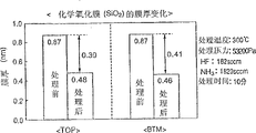
Fig. 6 is the optionally tables of data that silicon oxide layer beyond expression chemical oxide film and the chemical oxide film or silicon contain material.Fig. 7 is the block diagram of the data of presentation graphs 6, represents the data with " BTM " about " TOP " respectively.
Here the situation shown in Figure 5 that relative front has illustrated is to NH
3Gas is studied in the zone of denseer mixing ratio, and concrete is at HF gas: NH
3The flow-rate ratio of gas is to carry out in the zone of 1:10~1:50 scope.Treatment temperature herein, processing pressure and processing time are set at the mean value in the treatment conditions shown in Figure 5 respectively, and concrete is, setting treatment temperature respectively is 200 ℃, and processing pressure is 150Torr, and the processing time is 10 minutes.The gas of this operation in addition is by with NH
3Gas stuck-at-820sccm, and the flow of change HF gas changes the flow-rate ratio of two gases.In addition, the processing sheet number of wafer is 150.
Clear as can be known by Fig. 6 and Fig. 7, even with HF:NH
3Flow-rate ratio in the scope of 1:10~1:50, change by 1:10,1:20,1:50, the etch quantity (reduction) of poly-silicon fiml also is roughly zero, reduce hardly with poly-silicon fiml and relative to be, the etch quantity of chemical oxide film stably reduces in the scope of 0.41~0.57nm, thus, can confirm in the four corner of above-mentioned flow-rate ratio, with respect to poly-silicon fiml etching chemistry oxide-film optionally.
Along with the selection etching degree between chemical oxide film and SiN film, TEOS film and the heat oxide film is big more, its etch quantity is more little in addition.
Though SiN film, heat oxide film in addition are at HF:NH
3Than when the 1:10, the etch quantity of SiN film and heat oxide film, all roughly the same with the etch quantity of chemical oxide film, or many etching than the etch quantity of chemical oxide film.But, at HF:NH
3Than when the 1:20, the etch quantity of SiN film and heat oxide film, all lack than the etch quantity of chemical oxide film a lot, particularly at HF:NH
3When ratio was 1:50, the etch quantity of SiN film and heat oxide film all was roughly zero.Its result is in order to reduce chemical oxide film as best one can in inhibition SiN film, TEOS film and etched while of heat oxide film, as far as possible with NH
3Gas is that dense mixing ratio state is good, can confirm to preferably set HF:NH
3Ratio is in the scope of 1:20~1:50.
In addition, in the illustrated device of Fig. 1, in order easily to understand the present invention, to be provided with HF gas supply system 38 and NH
3 Gas supply system 40 is that example is illustrated for the situation of gas supply source, but is not limited to this situation, also can be provided with other and handle needed gas supply source and handle continuously.As an example, show the structure chart that the processing unit of gas supply system is used in the oxidation that merges the gas that is provided with supply steam or forms steam at Fig. 8.In addition, the structure division identical with structure division shown in Figure 1 uses prosign to indicate, to omit repeat specification.
As shown in Figure 8, be provided with above-mentioned HF gas supply system 38 and NH as the gas supply source herein
3Outside the gas supply system 40, also be provided with oxidation gas supply system 80.Concrete is with gas supply system 80, to be respectively equipped with H as this oxidation
2Gas source 80A and O
2Gas source 80B, these gases respectively by being provided with gas flow path 84A, the 84B of flow controller 82A, 82B, are imported in the container handling 18 by each gas nozzle 86A, 86B as required.
By such device with H
2Gas and O
2Gas supplies in the container handling 18, for example makes these gases produce steam in container handling 18 internal combustion, thus, for example implements thermal oxidation and forms heat oxide film on the surface of silicon substrate.
So,, beginning to supply with HF gas and NH if adopt this processing unit shown in Figure 8
3Gas is removed processing to the chemical oxide film attached to wafer surface, stops to supply with HF gas and NH afterwards
3Gas, then, by continuous supply H
2Gas and O
2Gas produces steam and carries out thermal oxidation, can form for example heat oxide film of grid oxidation film continuously.
In addition, also can be provided with gas supply system 80 as above-mentioned oxidation and make H
2Gas and O
2The external firing device that gas can burn uses the water vapor generation device that utilizes catalyst, and the steam that produces is imported in the container handling 18.
As another example, Fig. 7 shows and merges the structure chart that the silicon fiml that is provided with the gas of supplying with silicon fiml formation usefulness forms the processing unit of using gas supply system in addition.In addition, the structure division identical with structure division shown in Figure 1 uses prosign to indicate, and omits repeat specification.
As shown in Figure 9, be provided with above-mentioned HF gas supply system 38 and NH as the gas supply source herein
3Outside the gas supply system 40, also be provided with silicon fiml and form with gas supply system 90.Concrete is with gas supply system 90, to be provided with silane (SiH as this silicon fiml formation
4) gas source 90A, this gas by being provided with the gas flow path 94A of flow controller 92A, is imported in the container handling 18 by gas nozzle 96A as required.
Be provided with for example first germane (GeH that is used for importing simultaneously dopant (impurity) in addition as dopant source
4) gas source 90B, this gas by being provided with the gas flow path 94B of flow controller 92B, is imported in the container handling 18 by gas nozzle 96B as required.
By in container handling 18, supplying with silane and first germane, can form the silicon fiml (poly-silicon fiml) of the germanium that is imported into as dopant like this.
So,, beginning to supply with HF gas and NH if adopt this processing unit shown in Figure 9
3Gas is removed processing to the chemical oxide film attached to wafer surface, stops to supply with HF gas and NH then
3Gas, then, the germanium that also imports as impurity by continuous supply silane gas and first Germane gas can form silicon fiml continuously.At this moment, by suitably selecting temperature, also can form the epitaxial film that has been doped germanium.In addition can be further the apparatus structure of Fig. 8 and Fig. 9 be constituted and to carry out chemical oxide film continuously and remove the apparatus structure that grid oxidation film forms and the silicon gate electrode forms after handling.
What lift here is that the continuous situation that forms the silicon fiml that has imported heat oxide film or germanium is that example is illustrated after removing chemical oxide film, but also can form metal film or nitride film or other dielectric films after removing chemical oxide film.At this moment, as previously mentioned, can use method of the present invention, be not to remove chemical oxide film yet, but as previously mentioned, for example after removing natural oxide film, carry out aforesaid continuous processing.
In addition, processing unit with two-layer pipe is that example is illustrated in the above-described embodiment, this is an example only, the present invention also is applicable to for example processing unit of mono-layer tube structure, this moment, processing unit was for importing each gas by the below or the top of container handling, by top or below to carrying out the structure of vacuum exhaust in the container handling.
In addition, method of the present invention is not limited to the aforesaid batch-wise processing unit that once can carry out oxidation processes for the multi-disc semiconductor wafer, also is applicable to by the mounting table in container handling (supporting arrangement) to go up the single leaf formula processing unit that semiconductor wafer a slice a slice is carried out oxidation processes as the lamp heating or the heater heats of mounting, heater.
In addition,, have more than and be limited to semiconductor wafer, also be applicable to LCD substrate and glass substrate etc. as handled object.
As last explanation,, can bring into play the action effect of following excellence if adopt the removal method and the processing unit of silicon oxide layer of the present invention.
Adopt the application's invention, can be by using HF gas and NH
3The mist of gas is removed the silicon oxide layer that is formed on the handled object surface effectively.
In addition, can also and remove the silicon oxide layer that chemical oxide film constitutes with respect to the etching well of silicon materials selectivity.
In addition, can also and remove the silicon oxide layer that chemical oxide film constitutes with respect to the etching well of silicon nitride film selectivity.
In addition, can also be with respect to by TEOS (tetraethyl orthosilicate) formed silicon oxide layer selectivity etching well and remove the silicon oxide layer that chemical oxide film constitutes.
In addition, can also be with respect to heat oxide film (SiO
2) selectivity etching well and remove the silicon oxide layer that chemical oxide film constitutes.
Claims (3)
1. the removal method of a silicon oxide layer is used for can carrying out in the container handling of vacuum exhaust, removes the silicon oxide layer that is formed on the handled object surface, it is characterized in that:
Use HF gas and NH
3The mist of gas is removed described silicon oxide layer,
Described silicon oxide layer is the chemical oxide film that forms by chemical treatment, in order to obtain selectivity, treatment temperature is set in 200 ℃~600 ℃ the scope with respect to the described chemical oxide film of silicon nitride film,
Described HF gas and NH
3The flow-rate ratio of gas is set in the scope of 1:20~1:50.
2. the removal method of a silicon oxide layer is used for can carrying out in the container handling of vacuum exhaust, removes the silicon oxide layer that is formed on the handled object surface, it is characterized in that:
Use HF gas and NH
3The mist of gas is removed described silicon oxide layer,
Described silicon oxide layer is the chemical oxide film that forms by chemical treatment, in order to obtain selectivity, treatment temperature is set in 200 ℃~600 ℃ the scope with respect to the described chemical oxide film of thermal silicon dioxide film,
Described HF gas and NH
3The flow-rate ratio of gas is set in the scope of 1:20~1:50.
3. the removal method of silicon oxide layer as claimed in claim 1 or 2 is characterized in that, described processing pressure is set in 26Pa~1011Pa.
Applications Claiming Priority (2)
| Application Number | Priority Date | Filing Date | Title |
|---|---|---|---|
| JP2003117664 | 2003-04-22 | ||
| JP2003117664 | 2003-04-22 |
Related Parent Applications (1)
| Application Number | Title | Priority Date | Filing Date |
|---|---|---|---|
| CNB2004800110434A Division CN100377317C (en) | 2003-04-22 | 2004-04-20 | Method for removing silicon oxide film and processing apparatus |
Publications (2)
| Publication Number | Publication Date |
|---|---|
| CN101131929A CN101131929A (en) | 2008-02-27 |
| CN100533683C true CN100533683C (en) | 2009-08-26 |
Family
ID=33308046
Family Applications (2)
| Application Number | Title | Priority Date | Filing Date |
|---|---|---|---|
| CNB2004800110434A Expired - Fee Related CN100377317C (en) | 2003-04-22 | 2004-04-20 | Method for removing silicon oxide film and processing apparatus |
| CNB2007101616523A Expired - Fee Related CN100533683C (en) | 2003-04-22 | 2004-04-20 | Removing method for silicone oxide film |
Family Applications Before (1)
| Application Number | Title | Priority Date | Filing Date |
|---|---|---|---|
| CNB2004800110434A Expired - Fee Related CN100377317C (en) | 2003-04-22 | 2004-04-20 | Method for removing silicon oxide film and processing apparatus |
Country Status (5)
| Country | Link |
|---|---|
| US (1) | US7611995B2 (en) |
| KR (1) | KR101046523B1 (en) |
| CN (2) | CN100377317C (en) |
| TW (1) | TW200501254A (en) |
| WO (1) | WO2004095559A1 (en) |
Families Citing this family (30)
| Publication number | Priority date | Publication date | Assignee | Title |
|---|---|---|---|---|
| US7705385B2 (en) * | 2005-09-12 | 2010-04-27 | International Business Machines Corporation | Selective deposition of germanium spacers on nitride |
| US20100216296A1 (en) * | 2005-10-27 | 2010-08-26 | Yusuke Muraki | Processing Method and Recording Medium |
| US8343280B2 (en) * | 2006-03-28 | 2013-01-01 | Tokyo Electron Limited | Multi-zone substrate temperature control system and method of operating |
| US20070238301A1 (en) * | 2006-03-28 | 2007-10-11 | Cabral Stephen H | Batch processing system and method for performing chemical oxide removal |
| US7718032B2 (en) | 2006-06-22 | 2010-05-18 | Tokyo Electron Limited | Dry non-plasma treatment system and method of using |
| JP4994724B2 (en) * | 2006-07-07 | 2012-08-08 | 株式会社東芝 | Film forming apparatus and film forming method |
| JP4939864B2 (en) * | 2006-07-25 | 2012-05-30 | 東京エレクトロン株式会社 | Gas supply apparatus, gas supply method, thin film forming apparatus cleaning method, thin film forming method, and thin film forming apparatus |
| JP5211464B2 (en) * | 2006-10-20 | 2013-06-12 | 東京エレクトロン株式会社 | Oxidizer for workpiece |
| US7786016B2 (en) * | 2007-01-11 | 2010-08-31 | Micron Technology, Inc. | Methods of uniformly removing silicon oxide and a method of removing a sacrificial oxide |
| JP4776575B2 (en) | 2007-03-28 | 2011-09-21 | 株式会社東芝 | Surface treatment method, etching treatment method, and electronic device manufacturing method |
| US20100184297A1 (en) * | 2007-06-22 | 2010-07-22 | Mikio Takagi | Method for protecting semiconductor wafer and process for producing semiconductor device |
| KR101330707B1 (en) * | 2007-07-19 | 2013-11-19 | 삼성전자주식회사 | Method of forming Semiconducotr Device |
| US8252194B2 (en) | 2008-05-02 | 2012-08-28 | Micron Technology, Inc. | Methods of removing silicon oxide |
| KR100870914B1 (en) * | 2008-06-03 | 2008-11-28 | 주식회사 테스 | Dry etch method for silicon oxide |
| JP5158068B2 (en) * | 2009-02-20 | 2013-03-06 | 東京エレクトロン株式会社 | Vertical heat treatment apparatus and heat treatment method |
| JP5520552B2 (en) * | 2009-09-11 | 2014-06-11 | 株式会社日立国際電気 | Semiconductor device manufacturing method and substrate processing apparatus |
| CN102569020B (en) * | 2010-12-10 | 2015-01-14 | 有研新材料股份有限公司 | Method and device for removing cut oxidation films of 8-inch wafers |
| GB2487716B (en) | 2011-01-24 | 2015-06-03 | Memsstar Ltd | Vapour Etch of Silicon Dioxide with Improved Selectivity |
| JP5661523B2 (en) * | 2011-03-18 | 2015-01-28 | 東京エレクトロン株式会社 | Film forming method and film forming apparatus |
| JP5917861B2 (en) | 2011-08-30 | 2016-05-18 | 株式会社Screenホールディングス | Substrate processing method |
| JP6110848B2 (en) * | 2012-05-23 | 2017-04-05 | 東京エレクトロン株式会社 | Gas processing method |
| CN110735181A (en) * | 2013-08-09 | 2020-01-31 | 应用材料公司 | Method and apparatus for pre-cleaning substrate surface prior to epitaxial growth |
| JP6426489B2 (en) * | 2015-02-03 | 2018-11-21 | 東京エレクトロン株式会社 | Etching method |
| US10622205B2 (en) * | 2015-02-16 | 2020-04-14 | Tokyo Electron Limited | Substrate processing method and substrate processing apparatus |
| WO2017176027A1 (en) * | 2016-04-05 | 2017-10-12 | 주식회사 테스 | Method for selectively etching silicon oxide film |
| JP6726610B2 (en) * | 2016-12-13 | 2020-07-22 | 東京エレクトロン株式会社 | Etching method and substrate processing system |
| JP2018170387A (en) * | 2017-03-29 | 2018-11-01 | 東京エレクトロン株式会社 | Film growth method and vertical type thermal processing device |
| JP7038564B2 (en) * | 2018-02-22 | 2022-03-18 | 東京エレクトロン株式会社 | Film forming method and substrate processing equipment |
| JP6860537B2 (en) * | 2018-09-25 | 2021-04-14 | 株式会社Kokusai Electric | Cleaning methods, semiconductor device manufacturing methods, board processing devices, and programs |
| JP2022036756A (en) * | 2020-08-24 | 2022-03-08 | キオクシア株式会社 | Semiconductor device |
Family Cites Families (16)
| Publication number | Priority date | Publication date | Assignee | Title |
|---|---|---|---|---|
| DE68928402T2 (en) * | 1988-12-27 | 1998-03-12 | Toshiba Kawasaki Kk | Process for removing an oxide layer on a substrate |
| JP2902012B2 (en) | 1989-10-27 | 1999-06-07 | 国際電気株式会社 | Low pressure oxidation equipment |
| JP2853211B2 (en) | 1989-11-01 | 1999-02-03 | 富士通株式会社 | Method for manufacturing semiconductor device |
| US5268069A (en) * | 1991-10-28 | 1993-12-07 | International Business Machines Corporation | Safe method for etching silicon dioxide |
| JPH05326464A (en) | 1992-05-15 | 1993-12-10 | Dainippon Screen Mfg Co Ltd | Method for vapor-phase washing of substrate surface |
| JPH0697140A (en) * | 1992-09-14 | 1994-04-08 | Toshiba Corp | Semiconductor substrate processing method |
| US5282925A (en) | 1992-11-09 | 1994-02-01 | International Business Machines Corporation | Device and method for accurate etching and removal of thin film |
| JP2833946B2 (en) | 1992-12-08 | 1998-12-09 | 日本電気株式会社 | Etching method and apparatus |
| JPH06244153A (en) * | 1993-02-16 | 1994-09-02 | Matsushita Electric Ind Co Ltd | Dry etching method |
| JPH08195381A (en) | 1995-01-17 | 1996-07-30 | Fujitsu Ltd | Manufacture of semiconductor device |
| JPH1140770A (en) * | 1997-07-18 | 1999-02-12 | Nec Corp | Method and device for manufacturing semiconductor device |
| US6635185B2 (en) * | 1997-12-31 | 2003-10-21 | Alliedsignal Inc. | Method of etching and cleaning using fluorinated carbonyl compounds |
| JP3436256B2 (en) | 2000-05-02 | 2003-08-11 | 東京エレクトロン株式会社 | Method and apparatus for oxidizing object to be treated |
| US6335261B1 (en) * | 2000-05-31 | 2002-01-01 | International Business Machines Corporation | Directional CVD process with optimized etchback |
| US6926843B2 (en) * | 2000-11-30 | 2005-08-09 | International Business Machines Corporation | Etching of hard masks |
| KR100520600B1 (en) * | 2003-02-17 | 2005-10-10 | 주식회사 하이닉스반도체 | Method for fabricating capacitor of semiconductor device |
-
2004
- 2004-04-20 WO PCT/JP2004/005643 patent/WO2004095559A1/en active Application Filing
- 2004-04-20 KR KR1020057016676A patent/KR101046523B1/en active IP Right Grant
- 2004-04-20 US US10/552,262 patent/US7611995B2/en not_active Expired - Fee Related
- 2004-04-20 CN CNB2004800110434A patent/CN100377317C/en not_active Expired - Fee Related
- 2004-04-20 TW TW093110984A patent/TW200501254A/en not_active IP Right Cessation
- 2004-04-20 CN CNB2007101616523A patent/CN100533683C/en not_active Expired - Fee Related
Also Published As
| Publication number | Publication date |
|---|---|
| TW200501254A (en) | 2005-01-01 |
| KR101046523B1 (en) | 2011-07-04 |
| WO2004095559A1 (en) | 2004-11-04 |
| US20060216941A1 (en) | 2006-09-28 |
| CN100377317C (en) | 2008-03-26 |
| TWI331364B (en) | 2010-10-01 |
| US7611995B2 (en) | 2009-11-03 |
| CN1777980A (en) | 2006-05-24 |
| KR20060002805A (en) | 2006-01-09 |
| CN101131929A (en) | 2008-02-27 |
Similar Documents
| Publication | Publication Date | Title |
|---|---|---|
| CN100533683C (en) | Removing method for silicone oxide film | |
| TWI675122B (en) | Methods for depositing films on sensitive substrates | |
| KR20230039625A (en) | Chamber undercoat preparation method for low temperature ald films | |
| CN101154589B (en) | Form film build method and the device of silicon oxide layer | |
| TWI488220B (en) | Atomic layer deposition of silicon and silicon-containing films | |
| KR100980127B1 (en) | Film formation method and apparatus for semiconductor process, and computer readable medium | |
| KR101129741B1 (en) | Film formation apparatus for semiconductor process and method for using same | |
| US8080477B2 (en) | Film formation apparatus and method for using same | |
| TW202013479A (en) | Etching method and etching apparatus | |
| US8349401B2 (en) | Film formation apparatus and method for using same | |
| KR101131645B1 (en) | Film formation method and apparatus for semiconductor process | |
| KR101133402B1 (en) | Film formation apparatus for semiconductor process | |
| JP4039385B2 (en) | Removal method of chemical oxide film | |
| US5914000A (en) | Apparatus for manufacturing semiconductor device and method of removing silicon oxidation film | |
| JP7386679B2 (en) | Film-forming method and film-forming equipment | |
| JP2004343095A (en) | Cleaning method of heat processing equipment | |
| CN117238751A (en) | Epitaxial growth method and system and epitaxial wafer | |
| JP3806753B2 (en) | Thin film forming apparatus and method for semiconductor device | |
| JPH0382768A (en) | Method and device for forming metal oxide thin film | |
| JP2004266297A (en) | Manufacturing method of semiconductor device |
Legal Events
| Date | Code | Title | Description |
|---|---|---|---|
| C06 | Publication | ||
| PB01 | Publication | ||
| C10 | Entry into substantive examination | ||
| SE01 | Entry into force of request for substantive examination | ||
| C14 | Grant of patent or utility model | ||
| GR01 | Patent grant | ||
| CF01 | Termination of patent right due to non-payment of annual fee |
Granted publication date: 20090826 |
|
| CF01 | Termination of patent right due to non-payment of annual fee |