CN100492628C - Electronic assembly comprisnig substrate with embedded capacitors and methods of manufacture - Google Patents
Electronic assembly comprisnig substrate with embedded capacitors and methods of manufacture Download PDFInfo
- Publication number
- CN100492628C CN100492628C CNB01802999XA CN01802999A CN100492628C CN 100492628 C CN100492628 C CN 100492628C CN B01802999X A CNB01802999X A CN B01802999XA CN 01802999 A CN01802999 A CN 01802999A CN 100492628 C CN100492628 C CN 100492628C
- Authority
- CN
- China
- Prior art keywords
- substrate
- islands
- ground connection
- coupled
- terminal
- Prior art date
- Legal status (The legal status is an assumption and is not a legal conclusion. Google has not performed a legal analysis and makes no representation as to the accuracy of the status listed.)
- Expired - Fee Related
Links
Images


Classifications
-
- H—ELECTRICITY
- H01—ELECTRIC ELEMENTS
- H01L—SEMICONDUCTOR DEVICES NOT COVERED BY CLASS H10
- H01L23/00—Details of semiconductor or other solid state devices
- H01L23/48—Arrangements for conducting electric current to or from the solid state body in operation, e.g. leads, terminal arrangements ; Selection of materials therefor
- H01L23/50—Arrangements for conducting electric current to or from the solid state body in operation, e.g. leads, terminal arrangements ; Selection of materials therefor for integrated circuit devices, e.g. power bus, number of leads
-
- H—ELECTRICITY
- H05—ELECTRIC TECHNIQUES NOT OTHERWISE PROVIDED FOR
- H05K—PRINTED CIRCUITS; CASINGS OR CONSTRUCTIONAL DETAILS OF ELECTRIC APPARATUS; MANUFACTURE OF ASSEMBLAGES OF ELECTRICAL COMPONENTS
- H05K1/00—Printed circuits
- H05K1/16—Printed circuits incorporating printed electric components, e.g. printed resistor, capacitor, inductor
-
- H—ELECTRICITY
- H01—ELECTRIC ELEMENTS
- H01L—SEMICONDUCTOR DEVICES NOT COVERED BY CLASS H10
- H01L23/00—Details of semiconductor or other solid state devices
- H01L23/48—Arrangements for conducting electric current to or from the solid state body in operation, e.g. leads, terminal arrangements ; Selection of materials therefor
- H01L23/488—Arrangements for conducting electric current to or from the solid state body in operation, e.g. leads, terminal arrangements ; Selection of materials therefor consisting of soldered or bonded constructions
- H01L23/498—Leads, i.e. metallisations or lead-frames on insulating substrates, e.g. chip carriers
- H01L23/49822—Multilayer substrates
-
- H—ELECTRICITY
- H05—ELECTRIC TECHNIQUES NOT OTHERWISE PROVIDED FOR
- H05K—PRINTED CIRCUITS; CASINGS OR CONSTRUCTIONAL DETAILS OF ELECTRIC APPARATUS; MANUFACTURE OF ASSEMBLAGES OF ELECTRICAL COMPONENTS
- H05K1/00—Printed circuits
- H05K1/16—Printed circuits incorporating printed electric components, e.g. printed resistor, capacitor, inductor
- H05K1/162—Printed circuits incorporating printed electric components, e.g. printed resistor, capacitor, inductor incorporating printed capacitors
-
- H—ELECTRICITY
- H01—ELECTRIC ELEMENTS
- H01L—SEMICONDUCTOR DEVICES NOT COVERED BY CLASS H10
- H01L2224/00—Indexing scheme for arrangements for connecting or disconnecting semiconductor or solid-state bodies and methods related thereto as covered by H01L24/00
- H01L2224/01—Means for bonding being attached to, or being formed on, the surface to be connected, e.g. chip-to-package, die-attach, "first-level" interconnects; Manufacturing methods related thereto
- H01L2224/02—Bonding areas; Manufacturing methods related thereto
- H01L2224/04—Structure, shape, material or disposition of the bonding areas prior to the connecting process
- H01L2224/05—Structure, shape, material or disposition of the bonding areas prior to the connecting process of an individual bonding area
- H01L2224/0554—External layer
- H01L2224/0556—Disposition
- H01L2224/05571—Disposition the external layer being disposed in a recess of the surface
-
- H—ELECTRICITY
- H01—ELECTRIC ELEMENTS
- H01L—SEMICONDUCTOR DEVICES NOT COVERED BY CLASS H10
- H01L2224/00—Indexing scheme for arrangements for connecting or disconnecting semiconductor or solid-state bodies and methods related thereto as covered by H01L24/00
- H01L2224/01—Means for bonding being attached to, or being formed on, the surface to be connected, e.g. chip-to-package, die-attach, "first-level" interconnects; Manufacturing methods related thereto
- H01L2224/02—Bonding areas; Manufacturing methods related thereto
- H01L2224/04—Structure, shape, material or disposition of the bonding areas prior to the connecting process
- H01L2224/05—Structure, shape, material or disposition of the bonding areas prior to the connecting process of an individual bonding area
- H01L2224/0554—External layer
- H01L2224/05573—Single external layer
-
- H—ELECTRICITY
- H01—ELECTRIC ELEMENTS
- H01L—SEMICONDUCTOR DEVICES NOT COVERED BY CLASS H10
- H01L2224/00—Indexing scheme for arrangements for connecting or disconnecting semiconductor or solid-state bodies and methods related thereto as covered by H01L24/00
- H01L2224/01—Means for bonding being attached to, or being formed on, the surface to be connected, e.g. chip-to-package, die-attach, "first-level" interconnects; Manufacturing methods related thereto
- H01L2224/10—Bump connectors; Manufacturing methods related thereto
- H01L2224/15—Structure, shape, material or disposition of the bump connectors after the connecting process
- H01L2224/16—Structure, shape, material or disposition of the bump connectors after the connecting process of an individual bump connector
- H01L2224/161—Disposition
- H01L2224/16151—Disposition the bump connector connecting between a semiconductor or solid-state body and an item not being a semiconductor or solid-state body, e.g. chip-to-substrate, chip-to-passive
- H01L2224/16221—Disposition the bump connector connecting between a semiconductor or solid-state body and an item not being a semiconductor or solid-state body, e.g. chip-to-substrate, chip-to-passive the body and the item being stacked
- H01L2224/16225—Disposition the bump connector connecting between a semiconductor or solid-state body and an item not being a semiconductor or solid-state body, e.g. chip-to-substrate, chip-to-passive the body and the item being stacked the item being non-metallic, e.g. insulating substrate with or without metallisation
- H01L2224/16235—Disposition the bump connector connecting between a semiconductor or solid-state body and an item not being a semiconductor or solid-state body, e.g. chip-to-substrate, chip-to-passive the body and the item being stacked the item being non-metallic, e.g. insulating substrate with or without metallisation the bump connector connecting to a via metallisation of the item
-
- H—ELECTRICITY
- H01—ELECTRIC ELEMENTS
- H01L—SEMICONDUCTOR DEVICES NOT COVERED BY CLASS H10
- H01L2924/00—Indexing scheme for arrangements or methods for connecting or disconnecting semiconductor or solid-state bodies as covered by H01L24/00
- H01L2924/0001—Technical content checked by a classifier
- H01L2924/00014—Technical content checked by a classifier the subject-matter covered by the group, the symbol of which is combined with the symbol of this group, being disclosed without further technical details
-
- H—ELECTRICITY
- H01—ELECTRIC ELEMENTS
- H01L—SEMICONDUCTOR DEVICES NOT COVERED BY CLASS H10
- H01L2924/00—Indexing scheme for arrangements or methods for connecting or disconnecting semiconductor or solid-state bodies as covered by H01L24/00
- H01L2924/01—Chemical elements
- H01L2924/01078—Platinum [Pt]
-
- H—ELECTRICITY
- H01—ELECTRIC ELEMENTS
- H01L—SEMICONDUCTOR DEVICES NOT COVERED BY CLASS H10
- H01L2924/00—Indexing scheme for arrangements or methods for connecting or disconnecting semiconductor or solid-state bodies as covered by H01L24/00
- H01L2924/095—Indexing scheme for arrangements or methods for connecting or disconnecting semiconductor or solid-state bodies as covered by H01L24/00 with a principal constituent of the material being a combination of two or more materials provided in the groups H01L2924/013 - H01L2924/0715
- H01L2924/097—Glass-ceramics, e.g. devitrified glass
- H01L2924/09701—Low temperature co-fired ceramic [LTCC]
-
- H—ELECTRICITY
- H01—ELECTRIC ELEMENTS
- H01L—SEMICONDUCTOR DEVICES NOT COVERED BY CLASS H10
- H01L2924/00—Indexing scheme for arrangements or methods for connecting or disconnecting semiconductor or solid-state bodies as covered by H01L24/00
- H01L2924/15—Details of package parts other than the semiconductor or other solid state devices to be connected
- H01L2924/151—Die mounting substrate
- H01L2924/153—Connection portion
- H01L2924/1531—Connection portion the connection portion being formed only on the surface of the substrate opposite to the die mounting surface
- H01L2924/15311—Connection portion the connection portion being formed only on the surface of the substrate opposite to the die mounting surface being a ball array, e.g. BGA
-
- H—ELECTRICITY
- H05—ELECTRIC TECHNIQUES NOT OTHERWISE PROVIDED FOR
- H05K—PRINTED CIRCUITS; CASINGS OR CONSTRUCTIONAL DETAILS OF ELECTRIC APPARATUS; MANUFACTURE OF ASSEMBLAGES OF ELECTRICAL COMPONENTS
- H05K1/00—Printed circuits
- H05K1/02—Details
- H05K1/03—Use of materials for the substrate
- H05K1/0306—Inorganic insulating substrates, e.g. ceramic, glass
-
- H—ELECTRICITY
- H05—ELECTRIC TECHNIQUES NOT OTHERWISE PROVIDED FOR
- H05K—PRINTED CIRCUITS; CASINGS OR CONSTRUCTIONAL DETAILS OF ELECTRIC APPARATUS; MANUFACTURE OF ASSEMBLAGES OF ELECTRICAL COMPONENTS
- H05K1/00—Printed circuits
- H05K1/02—Details
- H05K1/11—Printed elements for providing electric connections to or between printed circuits
- H05K1/111—Pads for surface mounting, e.g. lay-out
- H05K1/112—Pads for surface mounting, e.g. lay-out directly combined with via connections
-
- H—ELECTRICITY
- H05—ELECTRIC TECHNIQUES NOT OTHERWISE PROVIDED FOR
- H05K—PRINTED CIRCUITS; CASINGS OR CONSTRUCTIONAL DETAILS OF ELECTRIC APPARATUS; MANUFACTURE OF ASSEMBLAGES OF ELECTRICAL COMPONENTS
- H05K1/00—Printed circuits
- H05K1/18—Printed circuits structurally associated with non-printed electric components
- H05K1/182—Printed circuits structurally associated with non-printed electric components associated with components mounted in the printed circuit board, e.g. insert mounted components [IMC]
- H05K1/185—Components encapsulated in the insulating substrate of the printed circuit or incorporated in internal layers of a multilayer circuit
-
- H—ELECTRICITY
- H05—ELECTRIC TECHNIQUES NOT OTHERWISE PROVIDED FOR
- H05K—PRINTED CIRCUITS; CASINGS OR CONSTRUCTIONAL DETAILS OF ELECTRIC APPARATUS; MANUFACTURE OF ASSEMBLAGES OF ELECTRICAL COMPONENTS
- H05K2201/00—Indexing scheme relating to printed circuits covered by H05K1/00
- H05K2201/01—Dielectrics
- H05K2201/0183—Dielectric layers
- H05K2201/0187—Dielectric layers with regions of different dielectrics in the same layer, e.g. in a printed capacitor for locally changing the dielectric properties
-
- H—ELECTRICITY
- H05—ELECTRIC TECHNIQUES NOT OTHERWISE PROVIDED FOR
- H05K—PRINTED CIRCUITS; CASINGS OR CONSTRUCTIONAL DETAILS OF ELECTRIC APPARATUS; MANUFACTURE OF ASSEMBLAGES OF ELECTRICAL COMPONENTS
- H05K2201/00—Indexing scheme relating to printed circuits covered by H05K1/00
- H05K2201/04—Assemblies of printed circuits
- H05K2201/049—PCB for one component, e.g. for mounting onto mother PCB
-
- H—ELECTRICITY
- H05—ELECTRIC TECHNIQUES NOT OTHERWISE PROVIDED FOR
- H05K—PRINTED CIRCUITS; CASINGS OR CONSTRUCTIONAL DETAILS OF ELECTRIC APPARATUS; MANUFACTURE OF ASSEMBLAGES OF ELECTRICAL COMPONENTS
- H05K2201/00—Indexing scheme relating to printed circuits covered by H05K1/00
- H05K2201/10—Details of components or other objects attached to or integrated in a printed circuit board
- H05K2201/10613—Details of electrical connections of non-printed components, e.g. special leads
- H05K2201/10621—Components characterised by their electrical contacts
- H05K2201/10674—Flip chip
-
- H—ELECTRICITY
- H05—ELECTRIC TECHNIQUES NOT OTHERWISE PROVIDED FOR
- H05K—PRINTED CIRCUITS; CASINGS OR CONSTRUCTIONAL DETAILS OF ELECTRIC APPARATUS; MANUFACTURE OF ASSEMBLAGES OF ELECTRICAL COMPONENTS
- H05K2201/00—Indexing scheme relating to printed circuits covered by H05K1/00
- H05K2201/10—Details of components or other objects attached to or integrated in a printed circuit board
- H05K2201/10613—Details of electrical connections of non-printed components, e.g. special leads
- H05K2201/10621—Components characterised by their electrical contacts
- H05K2201/10734—Ball grid array [BGA]; Bump grid array
-
- H—ELECTRICITY
- H05—ELECTRIC TECHNIQUES NOT OTHERWISE PROVIDED FOR
- H05K—PRINTED CIRCUITS; CASINGS OR CONSTRUCTIONAL DETAILS OF ELECTRIC APPARATUS; MANUFACTURE OF ASSEMBLAGES OF ELECTRICAL COMPONENTS
- H05K3/00—Apparatus or processes for manufacturing printed circuits
- H05K3/46—Manufacturing multilayer circuits
- H05K3/4611—Manufacturing multilayer circuits by laminating two or more circuit boards
- H05K3/4626—Manufacturing multilayer circuits by laminating two or more circuit boards characterised by the insulating layers or materials
- H05K3/4629—Manufacturing multilayer circuits by laminating two or more circuit boards characterised by the insulating layers or materials laminating inorganic sheets comprising printed circuits, e.g. green ceramic sheets
-
- H—ELECTRICITY
- H05—ELECTRIC TECHNIQUES NOT OTHERWISE PROVIDED FOR
- H05K—PRINTED CIRCUITS; CASINGS OR CONSTRUCTIONAL DETAILS OF ELECTRIC APPARATUS; MANUFACTURE OF ASSEMBLAGES OF ELECTRICAL COMPONENTS
- H05K3/00—Apparatus or processes for manufacturing printed circuits
- H05K3/46—Manufacturing multilayer circuits
- H05K3/4688—Composite multilayer circuits, i.e. comprising insulating layers having different properties
Abstract
To reduce switching noise, the power supply terminals of an integrated circuit die can be coupled to the respective terminals of at least one embedded capacitor in a multilayer ceramic substrate. In one embodiment, the capacitor is formed of at least one high permittivity layer. In another embodiment, several high permittivity layers are interleaved with conductive layers. Alternatively, the capacitor can comprise at least one embedded discrete capacitor. Also described are an electronic system, a data processing system, and various methods of manufacture.
Description
Related invention
The present invention relates to following invention, this invention is transferred to the identical assignee of the present invention, and this invention and the present invention submit on the same day, and this invention is:
Sequence number No.09/628705, exercise question: " comprising electronic assembly part and manufacture method " with embedded capacitors insert
TECHNICAL FIELD OF THE INVENTION
Present invention generally relates to electronic packing piece.Or rather, the present invention relates to a kind of electronic assembly part that comprises substrate, this substrate has one or more embedded capacitors that are used for reducing the switching noise in the high-frequency integrated circuit, the invention still further relates to relevant manufacture method.
The background of invention
Usually, by means of integrated circuit (IC) physically with on the electricity is coupled to the substrate of being made by organic material or ceramic material, and integrated circuit is assembled in the packaging part usually.One or more this IC packaging parts can physically with on the electricity be coupled to printed circuit board (PCB) (PCB), thereby form " electronic assembly part ".This " electronic assembly part " can be the parts of " electronic system ".Herein, " electronic system " is broadly defined as the product of any comprising " electronic assembly part ".The example of electronic system comprise computer (for example desktop computer, laptop computer, handheld computer, server etc.), radio communication device (for example cell phone, radio telephone, beeper etc.), computer peripheral hardware (for example printer, scanner, monitor etc.), entertainment device (for example television set, broadcast receiver, stereo, recorder, CD-audio player, video tape recorder, MP3 (animation expert group, audio layer 3 etc.) phonograph, or the like.
In field of electronic systems, for the performance that improves equipment with reduce production costs, between producer, exist continual competitive pressure.For all the more so the encapsulation of IC on substrate, the method for packing of each Dai Xin must provide more performance and size is littler usually promptly compacter.
The IC substrate can comprise in a large number by optionally graphically with metal level and one or more one or more lip-deep electronic component that is installed in substrate of isolation that metal interconnecting wires (being called " trace " herein) is provided.These electronic components are connected to other element of electronic system by comprising the multilayer conductive path of substrate trace on function.Substrate trace is being carried the signal that each electronic component of system for example transmits between the IC usually.Some IC has relatively large I/O (I/O) terminal and a large amount of power supply terminal and earth terminals.A large amount of I/O terminals, power supply terminal and earth terminal require substrate to contain relatively large trace.Some substrate requires the multilayer trace that all system interconnections are provided.
The trace that is arranged in different layers is fabricated on the access opening of plate (being also referred to as " plated-through-hole ") usually and is electrically connected.Can be by means of some layer or all layers making hole of passing substrate, then the inner surface in hole is electroplated or used electric conducting material such as copper or tungsten that the hole is filled and form access opening.
A kind of conventional method that IC is installed on the substrate is called as " controlled avalanche chip connects " (C4).In the process of making the C4 packaging part, solder bump that utilization can reflux or solder ball, the conducting terminal of IC element are that island (being commonly referred to " electrically contacting ") is welded direct to the corresponding island on the substrate surface.C4 technology is widely used owing to its fastness and simplicity.
The IC internal circuit of processor and so on works in more and more higher clock frequency, and when IC worked in more and more higher power level, switching noise may be brought up to unacceptable level.
Owing to above-mentioned reason and present technique skilled person read and understand following other reason that will understand after this specification, in the art, the method and apparatus that is used for encapsulating IC on substrate for reduce the problem relevant with the high power supply with high clock frequency such as switching noise as far as possible exists very big demand.
Brief description of the drawings
Fig. 1 is the block diagram of the electronic system that makes up an electronic assembly part with embedded capacitors at least according to an embodiment of the invention;
Fig. 2 shows the profile of the MULTILAYER SUBSTRATE with embedded capacitors according to an embodiment of the invention;
Fig. 3 shows the profile of the MULTILAYER SUBSTRATE with embedded capacitors according to another embodiment of the invention;
Fig. 4 shows the profile of the MULTILAYER SUBSTRATE with embedding discrete capacitor of a flexible embodiment according to the present invention;
Fig. 5 shows the curve of electric capacity to the area of the various dielectric materials that can be used in the substrate with embedded capacitors according to an embodiment of the invention;
Fig. 6 is a flow chart of making the method for the substrate that comprises embedded capacitors according to an embodiment of the invention; And
Fig. 7 is a flow chart of making the method for the electronic assembly part with the substrate that comprises embedded capacitors according to an embodiment of the invention.
The detailed description of embodiment of the present invention
In the following detailed description of embodiment of the present invention,, wherein show and to implement concrete preferred embodiment of the present invention with method for example with reference to the accompanying drawing that constitutes a part of the present invention.These embodiments have been carried out enough detailed description, so that person skilled in the art can implement the present invention, and it should be understood that the embodiment that can utilize other and make logic, machinery do not depart from design of the present invention and scope with the change of electricity.Therefore, it is restrictive that following description is not considered to, and scope of the present invention is only defined by claims.
The present invention provides a kind of solution by means of embedding one or more decoupling capacitors in MULTILAYER SUBSTRATE for the power transmission problem relevant with the existing encapsulation technology of the integrated circuit that runs on high clock speed and high power levels.Various embodiments have been described herein.In one embodiment, the IC tube core is directly mounted to the MULTILAYER SUBSTRATE that contains embedded capacitors.Embedding capacitor can be a discrete capacitor, or one or more layers capacitive material.
Fig. 1 is the block diagram of the electronic system 1 that makes up an electronic assembly part 4 with embedded capacitors at least according to an embodiment of the invention.Electronic system 1 only is to adopt an example of electronic system of the present invention.In this example, electronic system 1 comprises data handling system, and this data handling system comprises and is used for the system bus 2 of each element of coupled system.System bus 2 provides between each element of electronic system 1 and communicates to connect, and can be embodied as single bus, combination bus, or is realized in any other suitable mode.
The circuit that can be included in other type in the electronic assembly part 4 is custom circuit, application-specific integrated circuit (ASIC) (ASIC) etc., for example is used for one or more circuit (for example telecommunication circuit 7) of the wireless device of cell phone, beeper, portable computer, intercom and similar electronic system and so on.This IC can carry out the function of any other type.
Electronic system 1 can also comprise external memory storage 10, external memory storage 10 can comprise the one or more memories that are suitable for special purpose again, for example the driver of the mobile medium 16 main storage 12, one or more hard disk drive 14 and/or one or more disposal such as the floppy disk that occurs with the random-access memory (ram) form, CD (CD), the digital video disk (DVD).
Electronic system 1 can also comprise display device 8, loud speaker 9 and keyboard and/or controller 20, and keyboard and/or controller 20 can comprise mouse, tracking ball, game console, voice recognition device or make system user information can be input to electronic system 1 and/or receive any other device of information from electronic system 1.
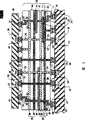
Fig. 2 shows the profile of the MULTILAYER SUBSTRATE with embedded capacitors 210 according to an embodiment of the invention.Substrate 210 has a plurality of island 211-213 on one surface, these islands can be coupled to each lead-in wire or conduction region 201-203 on the IC tube core 200 respectively via solder ball or solder bump 208.The holding wire that lead-in wire 201 is coupled to IC tube core 200, lead-in wire 202 is coupled to Vcc, 203 is coupled to Vss and go between.Be understandable that though identical reference number is used to two conductive paths of carrying signal level, that is comprises the path of the structure of being represented by reference number 201,208,211 and 221-223, these signals can be different.The signal path structure can comprise the various signal conductors that are expressed as in the ceramic substrate 210 such as the conductive layer of signal conductor 235-237.
Such as the signal lead or the projection of signal projection 201, the form with several row for example dark (for for simplicity, each side of tube core only shows delegation) is arranged at the tube core periphery usually.
The term of Shi Yonging " high dielectric constant layer " means the high dielectric constant material layer such as high-k titanate ceramics layer herein; Such as for example high dielectric constant film with the titanate film of sol-gel or the deposit of metal-organic chemical vapor deposition (MOCVD) method; Or the high dielectric constant material layer of any other type.
Tube core 200 and substrate 210 can be any kinds.In one embodiment, tube core 200 is processors, and substrate 210 is multi-layer ceramics substrates.
In embodiment shown in Figure 2, the metallization power channel hole 215 and 227 that is arranged in substrate 210 centers can be connected respectively to the tube core respective regions that can comprise relatively large Vss and Vcc die bump 203 and 202 respectively that is distributed in tube core 200 central areas with the Vss and the Vcc electric capacity dull and stereotyped 226 and 229 of capacitor 210.This massive parallel connects has guaranteed low-down inductance (for example less than 1 skin henry), and has improved the current carrying capacity of entire I C encapsulating structure.
The present invention can be applicable to signal traces equally and does not appear at the embodiment of tube core periphery and Vcc and Vss trace and be provided on the tube core Anywhere embodiment.
Be illustrated as being same as the die bump spacing though be appreciated that the spacing of power channel hole 215 among Fig. 2 and 227, power channel hole 215 and 227 spacing can be different from the spacing of die bump.Equally, though that the spacing in signalling channel hole 223 is illustrated as is wideer than die bump spacing, also can be identical in another embodiment.The physical dimension of access opening comprises the access opening spacing, can be in any suitable manner changes according to the design parameter known to the one skilled in the art.
Utilize the ceramic substrate technology can realize various embodiments.
A free-revving engine with substrate of embedded capacitors provides the bigger electric capacity of quite close tube core, so that reduce the influence of reactive induction coupling when IC moves, particularly under high clock speed.
Fig. 3 shows the profile of the substrate with embedded capacitors 310 according to another embodiment of the invention.In the embodiment depicted in fig. 3, substrate 310 can be coupled to another substrate 320.Substrate 320 can also can have IC tube core (not shown) similar in appearance to substrate 310 on its reverse side, maybe can be the substrate of printed circuit board (PCB) (PCB) or other types.The lead-in wire of substrate 320 or conductive region 334,339 and 319 can be coupled to the corresponding island 331,332 and 317 of substrate 310 via solder ball 338.
The internal structure of substrate 310 can be similar in appearance to the internal structure (Fig. 2) of above-mentioned substrate 210.Like this, substrate 310 a plurality ofly can be coupled to lead-in wire on the IC tube core 300 or the island 311-313 of conductive region 301-303 respectively via solder ball 308 just having on the one surface.The holding wire that lead-in wire 301 is coupled to IC tube core 300, lead-in wire 302 is coupled to Vcc, 303 is coupled to Vss and go between.Be understandable that though identical reference number is used to the conductive path of two kinds of carrying signal level, that is comprise the path of the structure of being represented by reference number 301,308,311 and 321-323, these signals also can be different.The signal path structure can comprise the various signal conductors that are shown the conductive layer in the substrate 310 such as signal conductor 335-337.
Tube core 300 and substrate 310 can be any kinds.In one embodiment, tube core 300 is processors, and substrate 310 is multi-layer ceramics substrates, and substrate 320 is PCB.In another embodiment, substrate 320 is ceramic substrate.
In the embodiment depicted in fig. 3, the metallization power channel hole 315,316 that is positioned at substrate 310 centers (should be noted that, each access opening section shown in Fig. 2 and 3, access opening section 315,316 and 327,328 for example, can be discrete access opening or continuous access opening) and 327,328, the respective regions that the Vss and the Vcc electric capacity dull and stereotyped 326 and 329 of capacitor 310 can be connected respectively to tube core, these zones can comprise the relatively large Vss that is distributed in tube core 300 each central areas and Vcc die bump 303 and 302 respectively.Low-down inductance (for example less than 1 skin henry) has been guaranteed in this big parallel connection.
Utilize ceramic substrate technology, can realize the various embodiments of substrate 310 and 320. Substrate 310 and 320 structure, comprise material therefor type, size, layer quantity, power conductor and signal conductor layout, or the like, constitute the requirement of its a part of electronic assembly part according to them, can be similar or different.
Island/the bump pitch that is appreciated that substrate 310 tops need be complementary with the bump pitch of tube core 300, and the island/bump pitch of substrate 310 bottoms need be complementary with the spot pitch of substrate 320.Though power channel hole 315 is identical at the top of substrate 320 with the bottom with 327 spacing in the embodiment depicted in fig. 3, and the signalling channel pitch of holes of substrate 320 bottoms is wideer than substrate 320 tops, but, can change the spacing relation in any suitable manner in order to satisfy design limit and purpose.
Fig. 4 shows the profile of the MULTILAYER SUBSTRATE 410 with two discrete capacitors 430 and 440 of a flexible embodiment according to the present invention.Substrate 410 can comprise multilayer Vcc, Vss and signal conductor, is used to install tube core 400 thereon.The lead-in wire 402 of substrate 410 is placed in the Vcc current potential, and can be coupled to corresponding conductive region (not shown) on the IC tube core 400 via certain solder ball 401.Equally, island 403 is placed in the Vss current potential, and can be coupled to the respective regions (not shown) on the IC tube core 400 via other solder ball 401.
Island 402 is comprised that the path in power channel hole 404, conductive layer 406 and power channel hole 412 is coupled to the upper terminal 426 of embedded capacitors 430.Island 403 is comprised that the path in power channel hole 405, conductive layer 407 and power channel hole 413 is coupled to other upper terminal 428 of embedded capacitors 430.
Island 431 is comprised that the path in power channel hole 418, conductive layer 416 and power channel hole 422 is coupled to the lower terminal 423 of embedded capacitors 430.Island 432 is comprised that the path in power channel hole 419, conductive layer 417 and power channel hole 424 is coupled to other lower terminal 425 of embedded capacitors 430.
As shown in Figure 4, the power channel hole, comprise power channel hole 404,405,412,413,418,419,422 and 424, be arranged in substrate 410 central areas that are in IC tube core 400 central areas belows basically (for for simplicity, the left-hand component of not shown IC tube core 400 and substrate 410).
As shown in Figure 4, can carry out the terminal of capacitor 440 being connected with Vss similar in appearance to the Vcc of capacitor 430.
The skilled person is understandable like that as the present technique field, in substrate 410, can also provide various signal paths (for for simplicity and not shown, but comprise on the signal area, some solder ball 410, substrate 410 of IC tube core 400 suitable island for example island 408 and 434 and substrate 410 in signal face and signalling channel hole 409 for example, signalling channel hole).
As shown in Figure 4, the signalling channel hole comprises signalling channel hole 409, is arranged in the outer peripheral areas (for for simplicity, the left-hand component of not shown IC tube core 400 and substrate 410) of the substrate 410 that is in the peripheral below of IC tube core 400 basically.
Embedded capacitors 430 and 440 can be any appropriate structuring.In one embodiment, these capacitors are ceramic chip capacitors made from conventional ceramic chip capacitor technology.Though show two capacitors 430 and 440 for simplicity in order to describe, in the embodiment depicted in fig. 4, can use the capacitor of different numbers, comprise and only use a capacitor.
Fig. 2-4 only is illustrative and drafting in proportion.Its some part may be exaggerated, and other parts may be reduced.Fig. 2-4 is used to illustrate the of the present invention various implementation methods that the general skilled person in present technique field can understand and implement rightly.
Make
Can with such as but be not limited to common process High Temperature Co Fired Ceramic (HTCC) technology, high thermal expansion coefficient (HITCE) technology or the glass ceramics technology, make the multi-layer ceramics substrate.
Though it is known to will be in ceramic process such as Al
2O
3And so on conventional ceramic membrane (for example 2 Mills) be clipped between the sheet metal and in ceramic substrate embedding low Dk capacitor, but in the embodiment in the present invention, adopted the multilayer laminated of high Dk layer.The high Dk layer that for example is used for making the ceramic chip capacitor can be buied on market.Suitable high Dk material such as the titanate particle can be inserted in the conventional ceramic substrate.In the present invention, such as BaTiO
3Multilayer laminated can the providing of high Dk up to 10_F/cm
2Electric capacity, by contrast, the electric capacity of low Dk layer is only in the scope of every square centimeter of millimicrofarad.
In a flexible embodiment, can be with the technology of knowing, for example metal organic chemical vapor deposition (MOCVD) technology or sol-gel technology form such as titanate film, for example (Ba in ceramic substrate
xSr
1-x) TiO
3(BST) or PbZrTiO
3(PZT) or Ta
2O
5Or SrTiO
3And so on high Dk layer, in sol-gel technology, as the colloidal sol of the solid particle colloidal suspensions in the liquid, owing to the growth of solid particle with interconnect and be transformed into gel.
Under two kinds of situations, high Dk material can both with ceramic process consistent temperature scope (for example 600-1000 ℃) in by embedding.
Be embedded in embodiment in the substrate 410 about discrete capacitor shown in Figure 4 430 and 440, by means of any routine techniques, for example punching press or laser ablation, can be near capacitor 430 and 440, and utilization requires consistent any proper metal metallization processes with technological temperature, and the Vcc of substrate 410 and Vss conductor can be coupled to the terminal of capacitor 430 and 440.
The estimation of electric capacity
Can estimate the capacitance values of embodiment shown in Figure 3 with equation 1.
Equation (1) C=A*-r*-o/d
Wherein: the A=capacitor sizes (square metre)
-r=dielectric constant 8.854 * 10
-12Farad/rice
The dielectric constant of-o=insulator
The thickness of d=dielectric layer (rice)
Fig. 5 shows the curve of the electric capacity (unit is a millimicrofarad) of the various dielectric materials that can be used in the substrate with embedded capacitors according to an embodiment of the invention to the capacitor length of side (unit is micron).Shown in Figure 5 is the curve of following dielectric material: curve 501 is PZT (Dk=2000), and curve 502 is BaTiO
3(Dk=1000), curve 503 is BST (Dk=500), curve 504 is SrTiO
x(Dk=200), and curve 505 is TaO
x(Dk=25).
Fig. 5 summed up with shown in the approximate range of various titanates and the oxide material electric capacity that can access.(for example use BaTiO when using the high-dielectric-constant ceramics layer
3The ceramic layer of dipping) time, the maximum capacitor that shown numerical value can access usually corresponding to the layer that with the thickness between Vcc layer and the Vss layer in the lamination that contains 40 this layers is 10 microns.
At the medium that forms with sol-gel or MOCVD embodiment (for example PZT, BST, SrTiO
3, or Ta
2O
5) situation under, the numerical value that calculates corresponding to shown in 0.25 micron membranes of medium.
In order to satisfy the electric capacity requirement of any given embodiment, can stacked on demand a plurality of capacitor layers.
Fig. 6 is a flow chart of making the method for the substrate that comprises embedded capacitors according to an embodiment of the invention.The method starts from 601.
In 603, in substrat structure, made a capacitor at least with first and second terminals.In one embodiment, this structure is a multilayer ceramic structure, though this structure can be made up of the material outside the ceramic material in other embodiment.Capacitor comprises (1), and at least one is clipped in high dielectric constant layer between each conductive layer; Perhaps, capacitor is (2) discrete capacitor.
In 605, in substrat structure, make first and second power supply nodes.Such as used herein, term " power supply node " refers to ground node (for example Vss) or with ground the power supply node (for example Vcc) of potential difference is arranged.
In 607, on the surface of substrat structure, make a plurality of islands, comprise and be coupled to the capacitor the first terminal and be coupled to first island of first power supply node and be coupled to capacitor second terminal and second island that is coupled to the second source node.First and second islands are oriented to be coupled to that treat will be by side by side to substrat structure surface and first and second power supply nodes of the tube core (for example IC tube core 200 of Fig. 2) that physically is fixed thereon.The method finishes at 609 places.
Fig. 7 is a flow chart of making the method for the electronic assembly part with the substrate that comprises embedded capacitors according to an embodiment of the invention.The method starts from 701.
In 703, provide tube core with first and second power supply nodes.
In 705, provide substrate with third and fourth power supply node.This substrate comprises at least one capacitor with first and second terminals.This capacitor comprises (1), and at least one is clipped in high dielectric constant layer between each conductive layer; Perhaps this capacitor is a discrete capacitor.This substrate also comprises its lip-deep a plurality of islands, comprises being coupled to the capacitor the first terminal and being coupled to first island of the 3rd power supply node and being coupled to capacitor second terminal and second island that is coupled to the 4th power supply node.
In 707, first and second islands are coupled to first and second power supply nodes of tube core respectively.The method finishes at 709 places.
Above-mentioned each operation of method shown in Fig. 6 and 7 can be carried out by being different from order described herein.
Conclusion
The method that the invention provides a kind of electronic assembly part and reduce problem such as the switching noise relevant with the high power transmission as far as possible with high clock frequency.Utilization can be satisfied the embedding decoupling capacitor with low inductance that for example power transmission of high-performance processor requires, and the invention provides adjustable big electric capacity (for example greater than every square centimeter 10 millifarad).Combining electronic system of the present invention can move under higher clock frequency, thereby at commercial more attractive.
As shown here, the present invention can realize in a large amount of different embodiments, comprises the method for substrate, electronic assembly part, electronic system, data handling system, making substrate and the method for making electronic assembly part.For the general skilled person in present technique field, other embodiment is conspicuous.The selection of capacity cell, material, geometry and electric capacity can both change to adapt to specific encapsulation requirement.The geometry in particular of embedded capacitors with regard to the component of its orientation, size, quantity, position and element thereof, is very flexibly.
Though having shown signal traces wherein, each embodiment provides around the periphery, and Vcc wherein and Vss trace are provided at die center, but the present invention can be applicable to signal traces equally and appears at embodiment beyond peripheral, and can be applicable to Vcc and Vss and be provided on the tube core Anywhere embodiment.
And the present invention is not limited to and is used in the C4 packaging part, can provide in the IC packaging part of any other type of advantage but can be used in characteristics of the present invention described herein.
Though described specific embodiment herein, the general skilled person in present technique field is understandable that, the specific embodiments shown in any arrangement that is suitable for reaching same purpose can replace.The application is considered to cover any correction of the present invention or change.Therefore, obvious the present invention only is subjected to the restriction of claim and equivalent thereof.
Claims (27)
1. electronic assembly part, it comprises:
The tube core that comprises power supply node, ground connection node, signal node; With
The multi-layer ceramics substrate, it comprises:
Embedded capacitors, this capacitor have the first terminal and second terminal;
The first surface of described multi-layer ceramics substrate, this first surface has first center and comprises first external zones of a plurality of signal islands, and this first center comprises a plurality of power supply islands that are coupled to described the first terminal and comprises a plurality of ground connection islands that are coupled to described second terminal;
The second surface of described multi-layer ceramics substrate, this second surface has second center and comprises second external zones of a plurality of signal islands, and this second center comprises a plurality of power supply islands that are coupled to described the first terminal and comprises a plurality of ground connection islands that are coupled to this second terminal;
Wherein these a plurality of power supply islands, a plurality of ground connection island, a plurality of signal island are coupled to one corresponding in the power supply node, ground connection node, signal node of described tube core.
2. electronic system, it comprises the electronic assembly part of the tube core that is coupled to the multi-layer ceramics substrate, and described tube core comprises power supply node, ground connection node, signal node, and this substrate comprises:
At least one embedded capacitors, this embedded capacitors have the first terminal and second terminal,
The first surface of described multi-layer ceramics substrate, this first surface has first center and comprises first external zones of a plurality of signal islands, and this first center comprises a plurality of power supply islands that are coupled to described the first terminal and comprises a plurality of ground connection islands that are coupled to described second terminal;
The second surface of described multi-layer ceramics substrate, this second surface has second center and comprises second external zones of a plurality of signal islands, and this second center comprises a plurality of power supply islands that are coupled to described the first terminal and comprises a plurality of ground connection islands that are coupled to this second terminal;
Wherein these a plurality of power supply islands, a plurality of ground connection island, a plurality of signal island are coupled to one corresponding in the power supply node, ground connection node, signal node of described tube core.
3. data handling system, it comprises:
The bus of each element in the coupling data treatment system;
Be coupled to the display of bus;
Be coupled to the external memory storage of bus; And
Be coupled to the processor of bus, and this processor comprises electronic assembly part,
This electronic assembly part comprises:
The tube core that has power supply node, ground connection node, signal node; With
The multi-layer ceramics substrate, it comprises:
Embedded capacitors, this capacitor have the first terminal and second terminal;
The first surface of described multi-layer ceramics substrate, this first surface has first center and comprises first external zones of a plurality of signal islands, and this first center comprises a plurality of power supply islands that are coupled to this first terminal and comprises a plurality of ground connection islands that are coupled to this second terminal;
The second surface of described multi-layer ceramics substrate, this second surface has second center and comprises second external zones of a plurality of signal islands, and this second center comprises a plurality of power supply islands that are coupled to described the first terminal and comprises a plurality of ground connection islands that are coupled to this second terminal;
Wherein these a plurality of power supply islands, a plurality of ground connection island, a plurality of signal island are coupled to one corresponding in the power supply node, ground connection node, signal node of described tube core.
4. method that is constructed for the multi-layer ceramics substrate of package die, this method comprises:
In the center of substrate, make a plurality of power supplys and ground connection access opening;
In the external zones of substrate, make a plurality of signalling channels hole;
In substrate, make embedded capacitors with the first terminal and second terminal; With
On substrate surface, make a plurality of via a plurality of power supply islands of a plurality of power channel hole with the first terminal coupling, a plurality of a plurality of ground connection islands that are coupled via a plurality of ground connection access openings and second terminal, and a plurality of signal islands that are coupled with a plurality of signalling channels hole;
Wherein a plurality of power supply islands, a plurality of ground connection island and a plurality of signal island are oriented to connect respective electrical source node, ground connection node, the signal node that solder bump is coupled to tube core by controlled avalanche chip.
5. the described method of claim 4, embedded capacitors wherein comprises a plurality of high dielectric constant layers.
6. the described method of claim 5, wherein said embedded capacitors is made up of a plurality of conductive layers that replace with this high dielectric constant layer, makes the conductive layer that replaces be coupled to described power supply island and ground connection island respectively.
7. the described method of claim 4, wherein said embedded capacitors is made up of at least one embedding discrete capacitor.
8. method of making electronic assembly part, it comprises:
Provide have power supply node, the tube core of ground connection node, signal node;
The multi-layer ceramics substrate is provided, and it comprises:
Embedded capacitors with first and second terminals;
The first surface of described multi-layer ceramics substrate, this first surface has first center and comprises first external zones of a plurality of signal islands, and this first center comprises a plurality of power supply islands that are coupled to this first terminal and comprises a plurality of ground connection islands that are coupled to this second terminal;
The second surface of described multi-layer ceramics substrate, this second surface has second center and comprises second external zones of a plurality of signal islands, and this second center comprises a plurality of power supply islands that are coupled to described the first terminal and comprises a plurality of ground connection islands that are coupled to this second terminal;
Wherein these a plurality of power supply islands, a plurality of ground connection island, a plurality of signal island are coupled to one corresponding in the power supply, ground connection, signal node of described tube core.
9. the described method of claim 8, wherein said embedded capacitors comprises a plurality of high dielectric constant layers.
10. the described method of claim 9, embedded capacitors wherein is made up of a plurality of conductive layers that replace with this high dielectric constant layer, makes the conductive layer that replaces be coupled to described power supply island and ground connection island respectively.
11. the described method of claim 8, wherein said embedded capacitors is made up of at least one embedding discrete capacitor.
12. the substrate of a package die, it comprises:
A plurality of power channel hole in the substrate center zone and ground connection access opening;
A plurality of signalling channels hole in the substrate outer peripheral areas;
Embedded capacitors with the first terminal and second terminal; And
A surface has: a plurality of signal islands that are coupled to a plurality of power supply islands of the first terminal, are coupled to a plurality of ground connection islands of second terminal and are coupled to a plurality of signalling channels hole via a plurality of ground connection access openings via a plurality of power channel hole;
A plurality of power supply islands wherein, a plurality of ground connection island, a plurality of signal island are oriented to connect in power supply node that solder bump is coupled to tube core, ground connection node, the signal node corresponding one by controlled avalanche chip.
13. the described substrate of claim 12, substrate wherein are the multi-layer ceramics substrates.
14. the described substrate of claim 12, the number of a plurality of power supply islands wherein is substantially equal to the number of a plurality of ground connection islands.
15. the described substrate of claim 12, substrate is not exclusively passed at least one power channel hole wherein.
16. the described substrate of claim 12, at least one ground connection access opening wherein not exclusively passes substrate.
17. the substrate of a package die, it comprises:
A plurality of power channel hole in the substrate center zone and ground connection access opening;
Embedded capacitors with the first terminal and second terminal;
The first surface of described substrate, it comprises via a plurality of power channel hole is coupled to a plurality of power supply islands of described the first terminal and a plurality of ground connection islands that are coupled to described second terminal via a plurality of ground connection access openings;
The second surface of described substrate, it comprises via a plurality of power channel hole is coupled to a plurality of power supply islands of the first terminal and a plurality of ground connection islands that are coupled to second terminal via a plurality of ground connection access openings;
A plurality of power supply islands wherein are oriented to be connected respective electrical source node and the ground connection node that solder bump is coupled to tube core by controlled avalanche chip with a plurality of ground connection islands.
18. the described substrate of claim 17, substrate wherein are the multi-layer ceramics substrates.
19. the described substrate of claim 17, the number of a plurality of power supply islands of wherein all is substantially equal to the number of all a plurality of ground connection islands.
20. the described substrate of claim 17, substrate is not exclusively passed at least one power channel hole wherein.
21. the described substrate of claim 17, at least one ground connection access opening wherein not exclusively passes substrate.
22. the substrate of a package die, it comprises:
A plurality of power channel hole in the substrate center zone and ground connection access opening;
A plurality of signalling channels hole in the substrate outer peripheral areas;
Embedded capacitors with the first terminal and second terminal;
First surface, it comprises a plurality of signal islands that are coupled to a plurality of power supply islands of described the first terminal, are coupled to a plurality of ground connection islands of described second terminal and are coupled to a plurality of signalling channels hole via a plurality of ground connection access openings via a plurality of power channel hole;
Second surface, it comprises a plurality of signal islands that are coupled to a plurality of power supply islands of the first terminal, are coupled to a plurality of ground connection islands of second terminal and are coupled to a plurality of signalling channels hole via a plurality of ground connection access openings via a plurality of power channel hole;
A plurality of power supply islands wherein, a plurality of ground connection island and a plurality of signal island are oriented to connect respective electrical source node, ground connection node and the signal node that solder bump is coupled to tube core by controlled avalanche chip.
23. the described substrate of claim 22, substrate wherein are the multi-layer ceramics substrates.
24. the described substrate of claim 22, the number of a plurality of power supply islands of wherein all is substantially equal to the number of all ground connection islands.
25. the described substrate of claim 22, substrate is not exclusively passed at least one power channel hole wherein.
26. the described substrate of claim 22, at least one ground connection access opening wherein not exclusively passes substrate.
27. the described substrate of claim 22, a plurality of signalling channels hole wherein is positioned at the outer peripheral areas of substrate.
Applications Claiming Priority (2)
| Application Number | Priority Date | Filing Date | Title |
|---|---|---|---|
| US09/631,037 US6611419B1 (en) | 2000-07-31 | 2000-07-31 | Electronic assembly comprising substrate with embedded capacitors |
| US09/631,037 | 2000-07-31 |
Publications (2)
| Publication Number | Publication Date |
|---|---|
| CN1470069A CN1470069A (en) | 2004-01-21 |
| CN100492628C true CN100492628C (en) | 2009-05-27 |
Family
ID=24529522
Family Applications (1)
| Application Number | Title | Priority Date | Filing Date |
|---|---|---|---|
| CNB01802999XA Expired - Fee Related CN100492628C (en) | 2000-07-31 | 2001-07-26 | Electronic assembly comprisnig substrate with embedded capacitors and methods of manufacture |
Country Status (9)
| Country | Link |
|---|---|
| US (1) | US6611419B1 (en) |
| EP (2) | EP1358675B1 (en) |
| JP (1) | JP2004505469A (en) |
| KR (1) | KR100591217B1 (en) |
| CN (1) | CN100492628C (en) |
| AT (1) | ATE360889T1 (en) |
| AU (1) | AU2001280850A1 (en) |
| DE (1) | DE60128145T2 (en) |
| WO (1) | WO2002011207A2 (en) |
Families Citing this family (95)
| Publication number | Priority date | Publication date | Assignee | Title |
|---|---|---|---|---|
| US7321485B2 (en) | 1997-04-08 | 2008-01-22 | X2Y Attenuators, Llc | Arrangement for energy conditioning |
| US7336468B2 (en) | 1997-04-08 | 2008-02-26 | X2Y Attenuators, Llc | Arrangement for energy conditioning |
| US9054094B2 (en) | 1997-04-08 | 2015-06-09 | X2Y Attenuators, Llc | Energy conditioning circuit arrangement for integrated circuit |
| US6970362B1 (en) * | 2000-07-31 | 2005-11-29 | Intel Corporation | Electronic assemblies and systems comprising interposer with embedded capacitors |
| JP4129717B2 (en) * | 2001-05-30 | 2008-08-06 | 株式会社ルネサステクノロジ | Semiconductor device |
| US7385286B2 (en) * | 2001-06-05 | 2008-06-10 | Matsushita Electric Industrial Co., Ltd. | Semiconductor module |
| WO2003007379A1 (en) * | 2001-07-12 | 2003-01-23 | Hitachi, Ltd. | Electronic circuit component |
| JP3967108B2 (en) * | 2001-10-26 | 2007-08-29 | 富士通株式会社 | Semiconductor device and manufacturing method thereof |
| US8749054B2 (en) | 2010-06-24 | 2014-06-10 | L. Pierre de Rochemont | Semiconductor carrier with vertical power FET module |
| JP2004079701A (en) * | 2002-08-14 | 2004-03-11 | Sony Corp | Semiconductor device and its manufacturing method |
| JP4243117B2 (en) * | 2002-08-27 | 2009-03-25 | 新光電気工業株式会社 | Semiconductor package, manufacturing method thereof, and semiconductor device |
| US6844505B1 (en) * | 2002-11-04 | 2005-01-18 | Ncr Corporation | Reducing noise effects in circuit boards |
| US20040231885A1 (en) * | 2003-03-07 | 2004-11-25 | Borland William J. | Printed wiring boards having capacitors and methods of making thereof |
| US7626828B1 (en) * | 2003-07-30 | 2009-12-01 | Teradata Us, Inc. | Providing a resistive element between reference plane layers in a circuit board |
| US8569142B2 (en) * | 2003-11-28 | 2013-10-29 | Blackberry Limited | Multi-level thin film capacitor on a ceramic substrate and method of manufacturing the same |
| US6943294B2 (en) * | 2003-12-22 | 2005-09-13 | Intel Corporation | Integrating passive components on spacer in stacked dies |
| US7132743B2 (en) * | 2003-12-23 | 2006-11-07 | Intel Corporation | Integrated circuit package substrate having a thin film capacitor structure |
| US7256980B2 (en) * | 2003-12-30 | 2007-08-14 | Du Pont | Thin film capacitors on ceramic |
| US20050154105A1 (en) * | 2004-01-09 | 2005-07-14 | Summers John D. | Compositions with polymers for advanced materials |
| US20070019789A1 (en) * | 2004-03-29 | 2007-01-25 | Jmar Research, Inc. | Systems and methods for achieving a required spot says for nanoscale surface analysis using soft x-rays |
| JP2005286112A (en) * | 2004-03-30 | 2005-10-13 | Airex Inc | Printed circuit board and its manufacturing method |
| KR101053587B1 (en) * | 2004-06-04 | 2011-08-03 | 엘지전자 주식회사 | Board Assembly for Remote Control of Washing Machine |
| US20060001149A1 (en) * | 2004-06-30 | 2006-01-05 | Victor Prokofiev | Packaged substrate having variable width conductors and a variably spaced reference plane |
| US7216406B2 (en) * | 2004-09-29 | 2007-05-15 | Intel Corporation | Method forming split thin film capacitors with multiple voltages |
| JP4843611B2 (en) | 2004-10-01 | 2011-12-21 | デ,ロシェモント,エル.,ピエール | Ceramic antenna module and manufacturing method thereof |
| US7501698B2 (en) * | 2004-10-26 | 2009-03-10 | Kabushiki Kaisha Toshiba | Method and system for an improved power distribution network for use with a semiconductor device |
| US7269029B2 (en) * | 2004-11-09 | 2007-09-11 | International Business Machines Corporation | Rapid fire test board |
| US7778038B2 (en) * | 2004-12-21 | 2010-08-17 | E.I. Du Pont De Nemours And Company | Power core devices and methods of making thereof |
| US7613007B2 (en) * | 2004-12-21 | 2009-11-03 | E. I. Du Pont De Nemours And Company | Power core devices |
| US20060158828A1 (en) * | 2004-12-21 | 2006-07-20 | Amey Daniel I Jr | Power core devices and methods of making thereof |
| TWI414218B (en) * | 2005-02-09 | 2013-11-01 | Ngk Spark Plug Co | Wiring board and capacitor to be built into wiring board |
| GB2439861A (en) | 2005-03-01 | 2008-01-09 | X2Y Attenuators Llc | Internally overlapped conditioners |
| US7548432B2 (en) * | 2005-03-24 | 2009-06-16 | Agency For Science, Technology And Research | Embedded capacitor structure |
| US7492570B2 (en) * | 2005-04-13 | 2009-02-17 | Kabushiki Kaisha Toshiba | Systems and methods for reducing simultaneous switching noise in an integrated circuit |
| US20060289976A1 (en) * | 2005-06-23 | 2006-12-28 | Intel Corporation | Pre-patterned thin film capacitor and method for embedding same in a package substrate |
| US8715839B2 (en) * | 2005-06-30 | 2014-05-06 | L. Pierre de Rochemont | Electrical components and method of manufacture |
| US8350657B2 (en) | 2005-06-30 | 2013-01-08 | Derochemont L Pierre | Power management module and method of manufacture |
| US7621041B2 (en) | 2005-07-11 | 2009-11-24 | E. I. Du Pont De Nemours And Company | Methods for forming multilayer structures |
| US7435627B2 (en) * | 2005-08-11 | 2008-10-14 | International Business Machines Corporation | Techniques for providing decoupling capacitance |
| US7701052B2 (en) | 2005-10-21 | 2010-04-20 | E. I. Du Pont De Nemours And Company | Power core devices |
| US7456459B2 (en) * | 2005-10-21 | 2008-11-25 | Georgia Tech Research Corporation | Design of low inductance embedded capacitor layer connections |
| US7705423B2 (en) * | 2005-10-21 | 2010-04-27 | Georgia Tech Research Corporation | Device having an array of embedded capacitors for power delivery and decoupling of high speed input/output circuitry of an integrated circuit |
| US7504706B2 (en) * | 2005-10-21 | 2009-03-17 | E. I. Du Pont De Nemours | Packaging having an array of embedded capacitors for power delivery and decoupling in the mid-frequency range and methods of forming thereof |
| US8520402B1 (en) * | 2005-10-25 | 2013-08-27 | Xilinx, Inc. | Decoupling capacitor circuit assembly |
| US8354294B2 (en) | 2006-01-24 | 2013-01-15 | De Rochemont L Pierre | Liquid chemical deposition apparatus and process and products therefrom |
| KR100744903B1 (en) | 2006-02-22 | 2007-08-01 | 삼성전기주식회사 | Multi-layer board with decoupling function |
| US20080019552A1 (en) * | 2006-03-27 | 2008-01-24 | Kurt Eldracher | Personal audio device accessory |
| US7848512B2 (en) * | 2006-03-27 | 2010-12-07 | Kurt Eldracher | Personal audio device accessory |
| US20070244267A1 (en) * | 2006-04-10 | 2007-10-18 | Dueber Thomas E | Hydrophobic crosslinkable compositions for electronic applications |
| US20070236859A1 (en) * | 2006-04-10 | 2007-10-11 | Borland William J | Organic encapsulant compositions for protection of electronic components |
| US20070291440A1 (en) * | 2006-06-15 | 2007-12-20 | Dueber Thomas E | Organic encapsulant compositions based on heterocyclic polymers for protection of electronic components |
| US7751205B2 (en) * | 2006-07-10 | 2010-07-06 | Ibiden Co., Ltd. | Package board integrated with power supply |
| TWI326908B (en) * | 2006-09-11 | 2010-07-01 | Ind Tech Res Inst | Packaging structure and fabricating method thereof |
| US7902662B2 (en) * | 2007-04-02 | 2011-03-08 | E.I. Du Pont De Nemours And Company | Power core devices and methods of making thereof |
| US7841075B2 (en) * | 2007-06-19 | 2010-11-30 | E. I. Du Pont De Nemours And Company | Methods for integration of thin-film capacitors into the build-up layers of a PWB |
| US7791896B1 (en) | 2007-06-20 | 2010-09-07 | Teradata Us, Inc. | Providing an embedded capacitor in a circuit board |
| TWI364824B (en) * | 2007-08-08 | 2012-05-21 | Advanced Semiconductor Eng | Semiconductor structure and method of fabricating the same |
| US8564967B2 (en) | 2007-12-03 | 2013-10-22 | Cda Processing Limited Liability Company | Device and method for reducing impedance |
| US7863724B2 (en) * | 2008-02-12 | 2011-01-04 | International Business Machines Corporation | Circuit substrate having post-fed die side power supply connections |
| US7959598B2 (en) | 2008-08-20 | 2011-06-14 | Asante Solutions, Inc. | Infusion pump systems and methods |
| FI20095110A0 (en) * | 2009-02-06 | 2009-02-06 | Imbera Electronics Oy | Electronic module with EMI protection |
| US8409963B2 (en) * | 2009-04-28 | 2013-04-02 | CDA Procesing Limited Liability Company | Methods of embedding thin-film capacitors into semiconductor packages using temporary carrier layers |
| US8391017B2 (en) * | 2009-04-28 | 2013-03-05 | Georgia Tech Research Corporation | Thin-film capacitor structures embedded in semiconductor packages and methods of making |
| US8952858B2 (en) | 2009-06-17 | 2015-02-10 | L. Pierre de Rochemont | Frequency-selective dipole antennas |
| US8922347B1 (en) | 2009-06-17 | 2014-12-30 | L. Pierre de Rochemont | R.F. energy collection circuit for wireless devices |
| KR101169531B1 (en) * | 2009-07-03 | 2012-07-27 | 가부시키가이샤 테라미크로스 | Semiconductor construct and manufacturing method thereof as well as semiconductor device and manufacturing method thereof |
| CN102668734B (en) * | 2009-12-24 | 2016-02-03 | 株式会社村田制作所 | Circuit module |
| US8552708B2 (en) | 2010-06-02 | 2013-10-08 | L. Pierre de Rochemont | Monolithic DC/DC power management module with surface FET |
| US9023493B2 (en) | 2010-07-13 | 2015-05-05 | L. Pierre de Rochemont | Chemically complex ablative max-phase material and method of manufacture |
| US8415781B2 (en) * | 2010-08-09 | 2013-04-09 | Ibiden Co., Ltd. | Electronic component and method for manufacturing the same |
| CN103180955B (en) | 2010-08-23 | 2018-10-16 | L·皮尔·德罗什蒙 | Power field effect transistor with resonant crystal tube grid |
| EP2636069B1 (en) | 2010-11-03 | 2021-07-07 | L. Pierre De Rochemont | Semiconductor chip carriers with monolithically integrated quantum dot devices and method of manufacture thereof |
| US20120292777A1 (en) * | 2011-05-18 | 2012-11-22 | Lotz Jonathan P | Backside Power Delivery Using Die Stacking |
| FR2987545B1 (en) * | 2012-02-23 | 2015-02-06 | Thales Sa | MULTILAYER PRINTED CIRCUIT COMPRISING LOW DIELECTRIC LOSS TRANSMISSION LINES AND METHOD THEREOF |
| KR101472628B1 (en) * | 2012-07-02 | 2014-12-15 | 삼성전기주식회사 | Capacitor embedded PCB(printed circuit board) |
| KR102078015B1 (en) | 2013-11-07 | 2020-04-07 | 삼성전기주식회사 | Low temperature co-fired ceramic substrate with embedded capacitors |
| TWI529906B (en) * | 2013-12-09 | 2016-04-11 | 矽品精密工業股份有限公司 | Manufacturing method of semiconductor package |
| US9628052B2 (en) * | 2014-02-18 | 2017-04-18 | Qualcomm Incorporated | Embedded multi-terminal capacitor |
| US9659850B2 (en) * | 2014-12-08 | 2017-05-23 | Qualcomm Incorporated | Package substrate comprising capacitor, redistribution layer and discrete coaxial connection |
| KR102365103B1 (en) * | 2014-12-12 | 2022-02-21 | 삼성전자주식회사 | Semiconductor |
| JP2016162904A (en) * | 2015-03-03 | 2016-09-05 | ルネサスエレクトロニクス株式会社 | Semiconductor device manufacturing method |
| US9971970B1 (en) | 2015-04-27 | 2018-05-15 | Rigetti & Co, Inc. | Microwave integrated quantum circuits with VIAS and methods for making the same |
| EP3374905A1 (en) | 2016-01-13 | 2018-09-19 | Bigfoot Biomedical, Inc. | User interface for diabetes management system |
| CN112933333B (en) | 2016-01-14 | 2023-03-28 | 比格福特生物医药公司 | Adjusting insulin delivery rate |
| US11538753B2 (en) | 2016-12-30 | 2022-12-27 | Intel Corporation | Electronic chip with under-side power block |
| US10978403B2 (en) | 2019-01-30 | 2021-04-13 | Delta Electronics, Inc. | Package structure and method for fabricating the same |
| USD874471S1 (en) | 2017-06-08 | 2020-02-04 | Insulet Corporation | Display screen with a graphical user interface |
| US11121301B1 (en) | 2017-06-19 | 2021-09-14 | Rigetti & Co, Inc. | Microwave integrated quantum circuits with cap wafers and their methods of manufacture |
| US10134712B1 (en) * | 2017-08-23 | 2018-11-20 | Micron Technology, Inc. | Methods and systems for improving power delivery and signaling in stacked semiconductor devices |
| USD928199S1 (en) | 2018-04-02 | 2021-08-17 | Bigfoot Biomedical, Inc. | Medication delivery device with icons |
| TW202038266A (en) * | 2018-11-26 | 2020-10-16 | 瑞典商斯莫勒科技公司 | Semiconductor assembly with discrete energy storage component |
| USD920343S1 (en) | 2019-01-09 | 2021-05-25 | Bigfoot Biomedical, Inc. | Display screen or portion thereof with graphical user interface associated with insulin delivery |
| US11202375B2 (en) * | 2019-04-29 | 2021-12-14 | Qualcomm Incorporated | Surface mount passive component shorted together |
| US11404388B2 (en) | 2019-04-29 | 2022-08-02 | Qualcomm Incorporated | Surface mount passive component shorted together and a die |
| USD977502S1 (en) | 2020-06-09 | 2023-02-07 | Insulet Corporation | Display screen with graphical user interface |
Family Cites Families (32)
| Publication number | Priority date | Publication date | Assignee | Title |
|---|---|---|---|---|
| US4926241A (en) | 1988-02-19 | 1990-05-15 | Microelectronics And Computer Technology Corporation | Flip substrate for chip mount |
| EP0359513A3 (en) | 1988-09-14 | 1990-12-19 | Hitachi, Ltd. | Semiconductor chip carrier and method of making it |
| US5060116A (en) | 1990-04-20 | 1991-10-22 | Grobman Warren D | Electronics system with direct write engineering change capability |
| US5177594A (en) | 1991-01-09 | 1993-01-05 | International Business Machines Corporation | Semiconductor chip interposer module with engineering change wiring and distributed decoupling capacitance |
| US5177670A (en) | 1991-02-08 | 1993-01-05 | Hitachi, Ltd. | Capacitor-carrying semiconductor module |
| JP2966972B2 (en) | 1991-07-05 | 1999-10-25 | 株式会社日立製作所 | Semiconductor chip carrier, module mounting the same, and electronic device incorporating the same |
| US5800575A (en) | 1992-04-06 | 1998-09-01 | Zycon Corporation | In situ method of forming a bypass capacitor element internally within a capacitive PCB |
| JPH05335183A (en) | 1992-05-28 | 1993-12-17 | Murata Mfg Co Ltd | Electronic component provided with multilayer board and manufacture thereof |
| US5354955A (en) | 1992-12-02 | 1994-10-11 | International Business Machines Corporation | Direct jump engineering change system |
| US5377139A (en) | 1992-12-11 | 1994-12-27 | Motorola, Inc. | Process forming an integrated circuit |
| JP3325351B2 (en) * | 1993-08-18 | 2002-09-17 | 株式会社東芝 | Semiconductor device |
| US5523619A (en) * | 1993-11-03 | 1996-06-04 | International Business Machines Corporation | High density memory structure |
| JP3309522B2 (en) | 1993-11-15 | 2002-07-29 | 株式会社村田製作所 | Multilayer substrate and manufacturing method thereof |
| US5639989A (en) | 1994-04-19 | 1997-06-17 | Motorola Inc. | Shielded electronic component assembly and method for making the same |
| US5469324A (en) | 1994-10-07 | 1995-11-21 | Storage Technology Corporation | Integrated decoupling capacitive core for a printed circuit board and method of making same |
| JPH08167630A (en) * | 1994-12-15 | 1996-06-25 | Hitachi Ltd | Chip connection structure |
| JPH08172274A (en) | 1994-12-20 | 1996-07-02 | Murata Mfg Co Ltd | Ceramic multilayer board |
| US5714801A (en) * | 1995-03-31 | 1998-02-03 | Kabushiki Kaisha Toshiba | Semiconductor package |
| US5818699A (en) | 1995-07-05 | 1998-10-06 | Kabushiki Kaisha Toshiba | Multi-chip module and production method thereof |
| US5691568A (en) | 1996-05-31 | 1997-11-25 | Lsi Logic Corporation | Wire bondable package design with maxium electrical performance and minimum number of layers |
| US5796587A (en) | 1996-06-12 | 1998-08-18 | International Business Machines Corporation | Printed circut board with embedded decoupling capacitance and method for producing same |
| US5745335A (en) | 1996-06-27 | 1998-04-28 | Gennum Corporation | Multi-layer film capacitor structures and method |
| US5949654A (en) | 1996-07-03 | 1999-09-07 | Kabushiki Kaisha Toshiba | Multi-chip module, an electronic device, and production method thereof |
| JP3405545B2 (en) * | 1996-10-31 | 2003-05-12 | サーノフ コーポレイション | Integrated electronic circuit |
| JP3882954B2 (en) | 1997-03-19 | 2007-02-21 | Tdk株式会社 | Chip type multilayer ceramic capacitor |
| US6072690A (en) * | 1998-01-15 | 2000-06-06 | International Business Machines Corporation | High k dielectric capacitor with low k sheathed signal vias |
| US6075427A (en) | 1998-01-23 | 2000-06-13 | Lucent Technologies Inc. | MCM with high Q overlapping resonator |
| US5939782A (en) * | 1998-03-03 | 1999-08-17 | Sun Microsystems, Inc. | Package construction for integrated circuit chip with bypass capacitor |
| US6218729B1 (en) * | 1999-03-11 | 2001-04-17 | Atmel Corporation | Apparatus and method for an integrated circuit having high Q reactive components |
| US6183669B1 (en) * | 1999-03-25 | 2001-02-06 | Murata Manufacturing Co., Ltd. | Paste composition, circuit board using the same, ceramic green sheet, ceramic substrate, and method for manufacturing ceramic multilayer substrate |
| US6252761B1 (en) | 1999-09-15 | 2001-06-26 | National Semiconductor Corporation | Embedded multi-layer ceramic capacitor in a low-temperature con-fired ceramic (LTCC) substrate |
| US6452776B1 (en) | 2000-04-06 | 2002-09-17 | Intel Corporation | Capacitor with defect isolation and bypass |
-
2000
- 2000-07-31 US US09/631,037 patent/US6611419B1/en not_active Expired - Lifetime
-
2001
- 2001-07-26 CN CNB01802999XA patent/CN100492628C/en not_active Expired - Fee Related
- 2001-07-26 EP EP01959277A patent/EP1358675B1/en not_active Expired - Lifetime
- 2001-07-26 JP JP2002516833A patent/JP2004505469A/en active Pending
- 2001-07-26 WO PCT/US2001/023721 patent/WO2002011207A2/en active IP Right Grant
- 2001-07-26 DE DE60128145T patent/DE60128145T2/en not_active Expired - Lifetime
- 2001-07-26 KR KR1020027004176A patent/KR100591217B1/en not_active IP Right Cessation
- 2001-07-26 EP EP04025966A patent/EP1515365B1/en not_active Expired - Lifetime
- 2001-07-26 AU AU2001280850A patent/AU2001280850A1/en not_active Abandoned
- 2001-07-26 AT AT01959277T patent/ATE360889T1/en not_active IP Right Cessation
Also Published As
| Publication number | Publication date |
|---|---|
| EP1358675A2 (en) | 2003-11-05 |
| EP1358675B1 (en) | 2007-04-25 |
| JP2004505469A (en) | 2004-02-19 |
| DE60128145D1 (en) | 2007-06-06 |
| KR100591217B1 (en) | 2006-06-22 |
| EP1515365A2 (en) | 2005-03-16 |
| CN1470069A (en) | 2004-01-21 |
| EP1515365B1 (en) | 2010-03-31 |
| US6611419B1 (en) | 2003-08-26 |
| WO2002011207A2 (en) | 2002-02-07 |
| KR20020042698A (en) | 2002-06-05 |
| ATE360889T1 (en) | 2007-05-15 |
| EP1515365A3 (en) | 2006-10-04 |
| WO2002011207A3 (en) | 2003-08-28 |
| DE60128145T2 (en) | 2008-01-03 |
| AU2001280850A1 (en) | 2002-02-13 |
Similar Documents
| Publication | Publication Date | Title |
|---|---|---|
| CN100492628C (en) | Electronic assembly comprisnig substrate with embedded capacitors and methods of manufacture | |
| CN100492629C (en) | Electronic assembly comprising interposer with embedded capacitors and methods of manufacture | |
| CN1284234C (en) | Ceramic/organic hybrid substrate with embedded capacitors and methods of manufacture | |
| KR100550480B1 (en) | Multiple tier array capacitor and methods of fabrication therefor | |
| US20060228855A1 (en) | Capacitor with co-planar electrodes | |
| US7986532B2 (en) | Split thin film capacitor for multiple voltages | |
| CN109478545A (en) | Glass substrate including passive glass equipment and semiconductor bare chip | |
| EP3140839B1 (en) | Embedded package substrate capacitor with configurable/controllable equivalent series resistance | |
| CN102638931B (en) | Electronic assembly, method for minimizing parasitic capacitance, and method for manufacturing circuit board structure | |
| CN102024565B (en) | Capacitor structure | |
| JP2007019292A (en) | Electronic component module and laminated substrate for it | |
| US20040211954A1 (en) | Compositive laminate substrate with inorganic substrate and organic substrate | |
| JP2001177008A (en) | Circuit board provided with built-in capacitor and semiconductor device using the same | |
| CN218647936U (en) | Semiconductor capacitor structure | |
| JP2000049436A (en) | Electronic circuit device |
Legal Events
| Date | Code | Title | Description |
|---|---|---|---|
| C06 | Publication | ||
| PB01 | Publication | ||
| C10 | Entry into substantive examination | ||
| SE01 | Entry into force of request for substantive examination | ||
| C14 | Grant of patent or utility model | ||
| GR01 | Patent grant | ||
| CF01 | Termination of patent right due to non-payment of annual fee |
Granted publication date: 20090527 Termination date: 20170726 |
|
| CF01 | Termination of patent right due to non-payment of annual fee |